JP2014146399A - Buffer member and electronic apparatus - Google Patents
Buffer member and electronic apparatus Download PDFInfo
- Publication number
- JP2014146399A JP2014146399A JP2013014675A JP2013014675A JP2014146399A JP 2014146399 A JP2014146399 A JP 2014146399A JP 2013014675 A JP2013014675 A JP 2013014675A JP 2013014675 A JP2013014675 A JP 2013014675A JP 2014146399 A JP2014146399 A JP 2014146399A
- Authority
- JP
- Japan
- Prior art keywords
- plate
- storage device
- buffer member
- members
- housing
- Prior art date
- Legal status (The legal status is an assumption and is not a legal conclusion. Google has not performed a legal analysis and makes no representation as to the accuracy of the status listed.)
- Pending
Links
Images

Abstract
Description
本発明は、電子機器に搭載される記憶装置に対する衝撃を軽減する緩衝部材、及び該緩衝部材を用いた電子機器に関する。 The present invention relates to a buffer member that reduces an impact on a storage device mounted on an electronic device, and an electronic device using the buffer member.
磁気ディスク装置、半導体メモリ、光ディスク装置等の記憶装置は小型軽量化が急速に進んでおり、ノートブック型のパーソナルコンピュータ(ノート型PC)だけでなく、タブレット型のパーソナルコンピュータ(タブレット型PC)や携帯型の音楽プレーヤー等の各種の電子機器に搭載されている。 Storage devices such as magnetic disk devices, semiconductor memories, and optical disk devices are rapidly becoming smaller and lighter. Not only notebook personal computers (notebook PCs) but also tablet personal computers (tablet PCs) It is installed in various electronic devices such as portable music players.
例えば、磁気ディスク装置は、回転する磁気ディスク上を、ヘッドを搭載したスライダが極わずかの間隔で浮上しながらデータの書き込みを行う。このため、記録動作モードにおいて外部から衝撃が加えられるとヘッドと磁気ディスクの間隔が変化したり、目標トラックからの位置ずれが発生したりして書き込みエラーが発生する可能性がある。 For example, a magnetic disk device writes data on a rotating magnetic disk while a slider on which a head is mounted floats at a very small interval. For this reason, when an external impact is applied in the recording operation mode, the distance between the head and the magnetic disk may change, or a positional deviation from the target track may occur, causing a write error.
このため、磁気ディスク装置等の記憶装置は、それ自体にさまざまな耐衝撃機能を備えているが、記憶装置を搭載する電子機器においても、記憶装置に対する衝撃を軽減する対策が必要とされている。記憶装置に対する衝撃を軽減する技術として、本出願人は磁気ディスク装置の衝撃を緩衝部材によって軽減する構成を提案している(例えば、特許文献1参照)。 For this reason, a storage device such as a magnetic disk device itself has various impact resistance functions. However, even in an electronic device equipped with the storage device, a measure for reducing the impact on the storage device is required. . As a technique for reducing the impact on the storage device, the present applicant has proposed a configuration in which the impact of the magnetic disk device is reduced by a buffer member (see, for example, Patent Document 1).
ところで、ノート型PC等の電子機器は、筐体内部に余分なスペースが少ないため、十分な衝撃軽減性能を有しつつも、記憶装置の取付作業や交換作業を容易に行えることが望ましい。また、利便性や拡張性等の観点からも、電子機器では、記憶装置を簡単に交換できることが好ましい。 By the way, it is desirable that an electronic device such as a notebook PC has a small amount of extra space inside the housing, so that it can easily mount and replace the storage device while having sufficient impact reduction performance. In addition, from the viewpoint of convenience and expandability, it is preferable that the storage device can be easily replaced in the electronic device.
本発明は、上記従来技術の課題を考慮してなされたものであり、記憶装置に対する衝撃を十分に軽減することができ、しかも組付作業や交換作業を容易に行うことを可能とする緩衝部材、及び該緩衝部材を用いた電子機器を提供することを目的とする。 The present invention has been made in view of the above-described problems of the prior art, and can sufficiently reduce the impact on the storage device, and can easily perform assembly work and replacement work. And an electronic device using the buffer member.
本発明に係る緩衝部材は、電子機器に搭載される記憶装置に対する衝撃を軽減する緩衝部材であって、前記記憶装置の連続する3つの側面を囲うように配置される3つの板状部材を有し、少なくとも1つの板状部材を変形可能に構成した枠体と、前記枠体の両側部に位置する2つの板状部材の内面から内方へとそれぞれ突出し、前記記憶装置の側面に設けられた係合穴に係合可能な弾性体のピンとを備えることを特徴とする。 The shock-absorbing member according to the present invention is a shock-absorbing member that reduces an impact on the storage device mounted on the electronic device, and has three plate-like members arranged so as to surround three continuous side surfaces of the storage device. And at least one plate-like member configured to be deformable, and two plate-like members located on both sides of the frame to project inward from the inner surfaces of the frame member, and are provided on the side surface of the storage device. And an elastic pin that can be engaged with the engaging hole.
また、本発明に係る電子機器は、緩衝部材を用いて記憶装置を弾性支持した状態で筐体の内部に収納する電子機器であって、前記緩衝部材は、前記記憶装置の連続する3つの側面を囲うように配置される3つの板状部材を有し、少なくとも1つの板状部材を変形可能に構成した枠体と、前記枠体の両側部に位置する2つの板状部材の内面から内方へとそれぞれ突出し、前記記憶装置の側面に設けられた係合穴に係合可能な弾性体のピンとを備え、前記記憶装置の係合穴に前記ピンが係合され、少なくとも前記枠体の両側部に位置する2つの板状部材の上端面及び下端面が前記筐体に当接した状態で、前記記憶装置が前記筐体の内部に収納されることを特徴とする。 The electronic device according to the present invention is an electronic device that is housed in a housing in a state in which the storage device is elastically supported using a buffer member, and the buffer member includes three continuous side surfaces of the storage device. A frame having three plate-like members arranged so as to surround the inner wall, and at least one plate-like member configured to be deformable, and the inner surfaces of the two plate-like members located on both sides of the frame An elastic body pin that protrudes in the direction and engages with an engagement hole provided on a side surface of the storage device, the pin being engaged with the engagement hole of the storage device, and at least the frame body The storage device is housed in the housing in a state in which upper and lower end surfaces of two plate-like members located on both sides are in contact with the housing.
このような構成によれば、緩衝部材は、板状部材を適宜変形させつつ、3つの板状部材で記憶装置の3つの側面を覆うと共に、弾性体のピンを記憶装置の係合穴に係合させることで記憶装置に取り付けることができる。このため、緩衝部材の記憶装置への組付作業及び交換作業が極めて容易に行うことができる。しかも、ピンが弾性体によって構成されるため、電子機器の筐体に付与された衝撃は、ピンで吸収されて記憶装置へはほとんど伝達されることがなく、記憶装置に対する衝撃を十分に軽減することができる。 According to such a configuration, the buffer member covers the three side surfaces of the storage device with the three plate-like members while appropriately deforming the plate-like member, and engages the elastic pin with the engagement hole of the storage device. By combining them, they can be attached to a storage device. For this reason, the work of assembling and replacing the buffer member to the storage device can be performed very easily. In addition, since the pin is formed of an elastic body, the impact applied to the housing of the electronic device is absorbed by the pin and hardly transmitted to the storage device, and the impact on the storage device is sufficiently reduced. be able to.
当該緩衝部材が前記記憶装置に取り付けられた状態で、少なくとも前記枠体の両側部に位置する2つの板状部材の上端面及び下端面は、前記記憶装置の上面及び下面よりも上方及び下方にそれぞれ突出した位置となることが好ましい。また、前記記憶装置が前記電子機器の内部に収納された状態で、該記憶装置の上面及び下面は、前記筐体から離間した位置にあることが好ましい。そうすると、緩衝部材を装着した記憶装置を電子機器内に搭載した場合に、少なくとも両側部に位置する2つの板状部材が筐体の天板と底板との間で支持され、記憶装置が弾性体であるピンによって筐体内で宙吊り状態で弾性的にフローティング支持される。従って、筐体に衝撃が加えられた場合であっても、記憶装置がフローティング状態で揺動するため、該記憶装置に伝達される衝撃を大幅に軽減することができる。 With the buffer member attached to the storage device, at least the upper and lower surfaces of the two plate-like members located on both sides of the frame body are above and below the upper and lower surfaces of the storage device. It is preferable to be in a protruding position. In addition, it is preferable that the upper surface and the lower surface of the storage device are in a position separated from the housing in a state where the storage device is housed in the electronic device. Then, when the storage device equipped with the buffer member is mounted in the electronic device, at least two plate-like members positioned on both sides are supported between the top plate and the bottom plate of the housing, and the storage device is an elastic body. The pin is elastically supported in a floating state in a suspended state in the casing. Therefore, even when an impact is applied to the housing, the storage device swings in a floating state, so that the impact transmitted to the storage device can be greatly reduced.
前記係合穴の内周面には、凹部が設けられており、前記ピンは、前記板状部材から突出した軸部と、該軸部よりも大径で先端側に設けられ、前記凹部と係合可能な係合爪部とを有すると、ピンを係合穴に挿入した際に、係合爪部が凹部に係合するため、ピンの確実な抜け止めを果たすことができ、さらに、挿入時には係合爪部と凹部との間でクリック音が生じるため、係合状態の把握が容易となり、組付作業の効率が一層向上する。 A concave portion is provided on the inner peripheral surface of the engagement hole, and the pin is provided with a shaft portion protruding from the plate-like member, a diameter larger than the shaft portion, and provided on the distal end side. With the engaging claw portion that can be engaged, when the pin is inserted into the engaging hole, the engaging claw portion engages with the concave portion, so that the pin can be securely removed, and Since a click sound is generated between the engaging claw portion and the concave portion at the time of insertion, the engagement state can be easily grasped and the efficiency of the assembling work is further improved.
この場合、前記係合穴は、ねじ穴であると、一般的な磁気ディスク装置等の記憶装置に設けられた固定用等のねじ穴を利用して、緩衝部材を固定することができる。また、係合穴をねじ穴とすると、その穴加工が容易となり、しかもピンとの係合位置を複数段設けておくことができるため、組立作業が一層容易なものとなり、取付後の安定性も向上する。 In this case, if the engagement hole is a screw hole, the buffer member can be fixed by using a screw hole for fixing provided in a storage device such as a general magnetic disk device. In addition, if the engagement hole is a screw hole, the hole can be easily machined, and the engagement position with the pin can be provided in a plurality of stages, so that the assembly work is further facilitated and the stability after mounting is also improved. improves.
前記枠体の両側部に位置する2つの板状部材の間を繋ぐ板状部材の内面には、前記記憶装置の側面に当接する弾性板が設けられていると、前後方向の衝撃を弾性板でも吸収することが可能となる。 When an elastic plate that contacts the side surface of the storage device is provided on the inner surface of the plate-like member that connects between the two plate-like members located on both sides of the frame body, the elastic plate absorbs the impact in the front-rear direction. But it can be absorbed.
前記枠体の両側部に位置する2つの板状部材の間を繋ぐ板状部材の外面には、当該緩衝部材を前記電子機器の筐体に対して固定するための取付孔を有する突出片が設けられてもよい。 On the outer surface of the plate-like member that connects between the two plate-like members located on both sides of the frame body, there are protruding pieces having attachment holes for fixing the buffer member to the housing of the electronic device. It may be provided.
本発明によれば、緩衝部材の記憶装置への組付作業及び交換作業が極めて容易に行うことができる。しかも、ピンが弾性体によって構成されるため、電子機器の筐体に付与された衝撃は、ピンで吸収されて記憶装置へはほとんど伝達されることがなく、記憶装置に対する衝撃を十分に軽減することができる。 According to the present invention, the work of assembling and replacing the buffer member to the storage device can be performed very easily. In addition, since the pin is formed of an elastic body, the impact applied to the housing of the electronic device is absorbed by the pin and hardly transmitted to the storage device, and the impact on the storage device is sufficiently reduced. be able to.
以下、本発明に係る緩衝部材について、この緩衝部材を用いた電子機器との関係で好適な実施の形態を挙げ、添付の図面を参照しながら詳細に説明する。 Hereinafter, the buffer member according to the present invention will be described in detail with reference to the accompanying drawings by giving preferred embodiments in relation to an electronic apparatus using the buffer member.
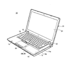
図1は、本発明の一実施形態に係る電子機器10の構成を示す斜視図である。電子機器10は、磁気ディスク装置(ハードディスクドライブ:HDD)からなる記憶装置12を、筐体14の内部に緩衝部材16を介して弾性支持した状態で収納することにより、筐体14から記憶装置12へと伝達される衝撃を軽減することができる。電子機器10としては、ノート型PC以外にも、タブレット型PCや携帯型の音楽プレーヤー等、各種の電子機器を例示できる。また、記憶装置12についても、磁気ディスク装置以外にも、半導体メモリや光ディスク装置等、電子機器に搭載される各種の記憶装置を例示できる。
FIG. 1 is a perspective view showing a configuration of an
図1に示すように、電子機器10は、一般的なノート型PCであり、筐体14と、筐体14の天板14aの一部に配置されるキーボード18と、筐体14の上面を開閉する蓋体20とを備える。筐体14は、天板14a及び底板14bを有し、内部に図示しない基板、演算装置、冷却装置、及びバッテリーパック等を収納した箱体であり、天板14aの開口部からキーボード18が上部に露出している。蓋体20は、筐体14に対し、ヒンジ22によって回動可能に設けられている。蓋体20の内面には、液晶等からなるディスプレイ24が設けられている。本実施形態の場合、記憶装置12は、筐体14内でキーボード18の手前右側となる位置に、緩衝部材16を介して収納・固定されている。
As illustrated in FIG. 1, the
次に、本実施形態に係る緩衝部材16の構成、及びこれを用いた記憶装置12の支持構造について説明する。
Next, the structure of the
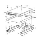
図2は、図1に示す電子機器10に搭載される記憶装置12から、本発明の一実施形態に係る緩衝部材16と、シールド部材26とを取り外した状態での分解斜視図である。図3は、図2に示す記憶装置12にシールド部材26を装着した状態での分解斜視図であり、図4は、図3に示す記憶装置12に緩衝部材16を取り付けた状態での斜視図である。また、図5は、緩衝部材16を介して記憶装置12を筐体14にフローティング状態で弾性支持した状態での縦断面図である。
FIG. 2 is an exploded perspective view of the
上記したように、本実施形態の場合、記憶装置12は、磁気ディスク装置(ハードディスクドライブ:HDD)であり、左右の側面12a,12cにねじ穴(係合穴)28がそれぞれ2つずつ設けられている。ねじ穴28は、磁気ディスク装置に一般的に設けられる規格上の取付穴である。記憶装置12において、図2中で後面となる側面12bは平坦な面であり、図2中で前面となる側面12dには電子機器10に設けられた図示しない配線コネクタが着脱される端子台29が設けられている。
As described above, in the case of this embodiment, the
シールド部材26は、薄い金属製の電磁波シールドフィルムである。シールド部材26は、両面テープや接着剤等により、側面12d及び上面12eを除く記憶装置12の側面12a〜12c及び下面12fに対して固着される(図3参照)。シールド部材26には、記憶装置12のねじ穴28を露出させるための逃げ孔26aが形成されている。
The
図2〜図4に示すように、緩衝部材(衝撃吸収ブラケット)16は、3つの板状部材30a,30b,30cで構成されたコの字状の枠体30と、枠体30の両側部(両端)で互いに向かい合う2つの板状部材30a,30cの内面から内方へと前後2箇所からそれぞれ突出した弾性体のピン32,34とを備える。
As shown in FIGS. 2 to 4, the buffer member (impact absorbing bracket) 16 includes a
枠体30は、記憶装置12に対して、3つの板状部材30a〜30cが連続する3つの側面12a〜12cをそれぞれ囲うように配置される。板状部材30a〜30cは、例えば樹脂材料や金属材料の薄板によって一体的に成形されており、隣接する板状部材30a〜30cの端部同士が直角に屈曲成形されることでコの字状の枠体30を構成している。3枚の薄板からなる板状部材30a〜30cを一体的に成形しているため、各板状部材30a〜30cは、少なくともその長手方向に交差する首振り方向に弾性変形可能となっている。
The
すなわち、両側部の板状部材30a,30cを手で把持して両側方に離間するように広げると、これら両側部の板状部材(アーム)30a,30cと中央の板状部材(ベース)30bの根元部分を基点として、各板状部材30a〜30cが弾性変形し、枠体30を容易に広げることができる(図3中の2点鎖線、及び図6も参照)。枠体30は、1枚の長尺な薄板を2箇所で直角に屈曲させることで3枚の板状部材30a〜30cとして構成したものであってもよい。
That is, when the plate-
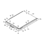
各板状部材30a〜30cの上端面には、その長手方向の大部分に渡って上方に突出する突出板36が設けられている。突出板36は、記憶装置12に緩衝部材16を取り付けた状態で、その上端面37aが記憶装置12の上面12eより上方に、例えば0.75mm程度突出した位置となり、筐体14の天板14aに当接する(図5参照)。また、図5から明らかな通り、記憶装置12に緩衝部材16を取り付けた状態で、板状部材30a〜30cの下端面37bは、記憶装置12の下面12fより下方に、例えば0.75mm程度突出した位置となり、筐体14の底板14bに当接する。突出板36を設けることにより、緩衝部材16の筐体14(天板14a)への位置決めが容易となり、また衝撃吸収性能も向上する。勿論、突出板36は省略してもよく、また、枠体30の下端面にも突出板36と同様なものを設けてもよい。
A protruding
なお、図5には図示していないが、両側部の板状部材30a,30cの上端面37a及び下端面37bのみならず、中央の板状部材30bの上端面37a及び下端面37bについても筐体14の天板14a及び底板14bに当接支持される。但し、中央の板状部材30bは必ずしも筐体14に当接支持される必要はなく、少なくともピン32,34が設けられた両側部の板状部材30a,30cが筐体14に当接支持されていればよい。
Although not shown in FIG. 5, not only the
中央の板状部材30bの外面中央部には、外方へと突出する金属製の薄板からなる突出片38が設けられている。突出片38は、その基端部38aを板状部材30bの中央部に形成された孔部39に挿通させて上下左右に折り曲げることで該板状部材30bに固定されている(図2参照)。突出片38の略中央には、板厚方向に貫通する取付孔38bが形成されている(図3参照)。取付孔38bは、緩衝部材16を装着した記憶装置12を電子機器10の筐体14に固定する際に、固定ねじ40を挿通させる孔部である(図1及び図5参照)。
A projecting
中央の板状部材30bの内面には、突出片38の取付部となる孔部39の両脇に、一対の弾性板41,41が設けられている。弾性板41は、板状部材30bに固着された薄板状のゴムシートであり、後述の基部42と同様に2色成形によって板状部材30bに固定されている。
On the inner surface of the central plate-
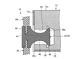
次に、ピン32,34は、図2に示すように、両側部の板状部材30a,30cに対してそれぞれ固着された帯状の基部42の内面の前後2箇所から内方へと突出している。ピン32,34及び基部42は、ゴム材料等からなる弾性体で形成されている。ピン32,34及び基部42は、両側部の板状部材30a,30cに対して2色成形(ダブルモールド)によって固着され、ピン32,34と基部42は一体成形となっている。より具体的には、図5に示すように、基部42は、板状部材30a,30cの長手方向に沿って形成された板厚方向の段付き孔部44を埋めるように2色成形され、その内面側にピン32,34を突出させている。
Next, as shown in FIG. 2, the
このように弾性体で形成されたピン32,34は、図5に示すように、基部42から突出する軸部(中間部)46と、軸部46よりも大径で先端側に設けられ、記憶装置12のねじ穴28の凹部28aと係合可能な係合爪部(嵌合部、拡径部)48とを備える。これにより、ピン32,34は、基端側(基部42側)から先端側に向かって、軸部46で一旦縮径した後、係合爪部48で再び拡径する滑らかな段付き形状となっている。ピン32,34の形状は、基端側から先端側に向かって同径で延び、先端にのみ拡径したリング状の係合爪部を設けた形状であってもよく、さらには、基端側から先端側まで同径又は略同径の円柱形状であってもよく、要は、ねじ穴28に嵌合可能な形状であればよい。
As shown in FIG. 5, the
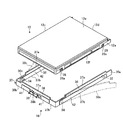
図6に、緩衝部材16の記憶装置12への取付方法の一例を模式的に示す。
FIG. 6 schematically shows an example of a method for attaching the
緩衝部材16を記憶装置12に取り付ける場合には、先ず、図6(A)に示すように、両側部の板状部材30a,30cのうち、一方の板状部材30cを記憶装置12の側面12cに対応配置し、その内面のピン32,34を各ねじ穴28へと挿入して適度な位置まで進入させ、係合爪部48を所定の凹部28aに係合させる。なお、緩衝部材16を取り付けるのに先立ち、記憶装置12にはシールド部材26が予め装着されている
When attaching the
続いて、図6(A)に示すように、記憶装置12の側面12cに固定した板状部材30cを基点とし、中央の板状部材30b及び他方の板状部材30aを外方へと変形させつつ、これら板状部材30a,30bの内面を記憶装置12の側面12a,12bに対応配置させる。なお、本実施形態では、全ての板状部材30a〜30cが変形可能な構成を例示しているが、図6から明らかな通り、3つの板状部材30a〜30cのうち、少なくとも1つが変形可能であれば、緩衝部材16(枠体30)を記憶装置12の周囲に配置することが可能である。
Subsequently, as shown in FIG. 6A, the central plate-
そして、図6(B)に示すように、中央の板状部材30bの内面の弾性板41を記憶装置12の側面12bに当接させ、さらに、他方の板状部材30aの内面のピン32,34を記憶装置12の側面12aの各ねじ穴28へと挿入して適度な位置まで進入させ、係合爪部48を所定の凹部28aに係合させる。これにより、緩衝部材16が記憶装置12に対して固定されるため、必要に応じて、両側部の板状部材30a,30cを記憶装置12側にさらに押圧し、板状部材30a,30cがぐらつかない位置までピン32,34をねじ穴28内の奥部へと押し込んで凹部28aと係合させる。
Then, as shown in FIG. 6B, the
以上により、緩衝部材16の記憶装置12への固定が完了する(図4、図5及び図6(B)参照)。
Thus, the fixing of the
続いて、緩衝部材16が装着された記憶装置12を電子機器10に取り付ける場合には、先ず、筐体14の底板14bを取り外した状態で、図5に示すように、筐体14の内部の所定位置に緩衝部材16を装着した記憶装置12を載置する。そして、突出片38の取付孔38bに固定ねじ40を挿通させ、天板14a側の図示しないねじ穴に締結する。そうすると、板状部材30a〜30cの上端面37aが天板14aの内面に着地した状態となる。
Subsequently, when attaching the
そこで、底板14bを図示しない止めねじ等を用いて固定することにより、板状部材30a〜30cの下端面37bが底板14bの内面に着地した状態となり、緩衝部材16が天板14aと底板14bとの間で突っ張った状態で挟持・支持される。これにより、図5に示すように、弾性体であるピン32,34によって記憶装置12が筐体14内で宙吊り状態で弾性的にフローティング支持される。従って、筐体14に衝撃が加えられた場合であっても、図5中に矢印で示すように記憶装置12がフローティング状態で揺動するため、伝達される衝撃は大幅に軽減されることになる。
Therefore, by fixing the
以上のように、本実施形態に係る緩衝部材16によれば、記憶装置12の連続する3つの側面12a〜12cを囲うように配置される3つの板状部材30a〜30cを有し、少なくとも1つを変形可能に構成した枠体30と、枠体30の両側部に位置する2つの板状部材30a,30cの内面から内方へとそれぞれ突出し、記憶装置12の側面12a,12cに設けられた係合穴であるねじ穴28に係合可能な弾性体のピン32,34とを備える。
As described above, the shock-absorbing
従って、緩衝部材16では、3つの板状部材30a〜30cを適宜変形させつつ、3つの板状部材30a〜30cで記憶装置12の3つの側面12a〜12cを覆うと共に、弾性体のピン32,34を記憶装置12のねじ穴28に係合させることで記憶装置12に取り付けることができる(図6参照)。このため、緩衝部材16の記憶装置12への組付作業及び交換作業を極めて容易に行うことができる。しかも、ピン32,34が弾性体によって構成されるため、電子機器10の筐体14に付与された衝撃は、ピン32,34での弾性的なせん断変形により吸収されるため、記憶装置12へはほとんど伝達されることがなく、記憶装置12に対する衝撃を十分に軽減することができる。
Therefore, in the
緩衝部材16は、3つの板状部材30a〜30cによってコの字状(U字状)の枠体30を構成しているため、作業者が手で把持し易く記憶装置12への組付けが容易である。反面、記憶装置12から取り外す際には作業者等が意図的に両側部の板状部材30a,30cのピン32,34をねじ穴28から引き抜く必要がある。このため、緩衝部材16が意図せずに記憶装置12から外れてしまうことを回避することができると共に、意図して取り外したい場合には、ピン32,34をねじ穴28から引き抜けくだけでよいため、交換作業等が容易である。
Since the
緩衝部材16は、枠体30及び該枠体30に固定したピン32,34で構成され、取り扱い上は1部品のみの構成となっている。このため、緩衝部材16は、記憶装置12への取付作業が容易であり、製造時の量産性も高い。しかも、記憶装置12は、緩衝部材16を取り付けた状態であっても、その外形は薄い板状部材30a〜30cの板厚分のみが大きくなるだけとなり、重量の増加も少ないものとなる。このため、筐体14の内部での収納スペースが小さい場合であっても緩衝部材16を取り付けた記憶装置12を容易に収納することができ、電子機器10の小型・薄型化、さらに軽量化も可能となる。
The
図5に示すように、緩衝部材16が記憶装置12に取り付けられた状態で、少なくとも枠体30の両側部に位置する2つの板状部材30a,30cの上端面37a及び下端面37bは、記憶装置12の上面12e及び下面12fよりも上方及び下方にそれぞれ突出した位置となる。換言すれば、記憶装置12が電子機器10の内部に収納された状態で、該記憶装置12の上面12e及び下面12fは、筐体14から、例えば0.75mm程度離間した位置にある。
As shown in FIG. 5, the
これにより、緩衝部材16を装着した記憶装置12を電子機器10内に搭載した場合に、板状部材30a,30cが筐体14の天板14aと底板14bとの間で突っ張った状態で挟持・支持され、弾性体であるピン32,34によって記憶装置12が筐体14内で宙吊り状態で弾性的にフローティング支持される。従って、筐体14に衝撃が加えられた場合であっても、記憶装置12がフローティング状態で揺動するため、該記憶装置12に伝達される衝撃を大幅に軽減することができる。換言すれば、緩衝部材16では、ピン32,34の径を変更するだけで、ピン32,34のばね定数を適宜設定変更することができるため、各種の重量や外形からなる記憶装置12に最適なばね定数を有する衝撃吸収構造を容易に構築することができる。
As a result, when the
記憶装置12のねじ穴28の内周面には、凹部28aが設けられており、ピン32,34は、板状部材30a,30cから突出した軸部46と、該軸部46よりも大径で先端側に設けられ、凹部28aと係合可能な係合爪部48とを有する。これにより、ピン32,34をねじ穴28に挿入した際に、係合爪部48が凹部28aに係合するため、ピン32,34の確実な抜け止めを果たすことができる。さらに、ピン32,34の挿入時には係合爪部48とねじ穴28の凹凸形状との間でクリック音が生じるため、係合状態の把握が容易となり、組付作業の効率が一層向上する。また、ピン32,34では、先端側に大径の係合爪部48を設けたため、ねじ穴28に対して組付け易く且つ外れにくい形状となっており、緩衝部材16の組立性及び取付後の安定性が一層向上する。
A
この場合、ピン32,34が係合する記憶装置12の係合穴をねじ穴28とすると、一般的な磁気ディスク装置に設けられた固定用のねじ穴28を利用して、緩衝部材16を固定することができ、汎用性も高い。また、係合穴をねじ穴28とすると、その穴加工が容易となり、しかもピン32,34との係合位置を複数段設けておくことができるため係合位置の調整が容易となる。さらに、係合時のクリック音が連続的に発生するため、組立作業も一層容易なものとなる。
In this case, assuming that the engaging hole of the
ピン32,34を係合させる記憶装置12側の係合穴は、ねじ穴28以外であってもよく、ピン32,34の係合爪部48と係合可能な凹凸形状を有する穴であればよい。例えば、図7に示すように、ねじ穴28に代えて、凹部50aが奥側に1箇所形成された係合穴50として形成してもよい。また、ピン32,34と係合穴とは互いに係合可能(嵌合可能)であればよいことから、必ずしも互いの凹凸形状(係合爪部48、及び凹部28a,50a)は必要ではなく、例えば、弾性体であるピンの外径を係合穴の内径よりも多少大きく形成しておき、その抜け止めを図った構成等としてもよい。
The engaging hole on the
緩衝部材16では、枠体30の両側部の板状部材30a,30cの間を繋ぐ中央の板状部材30bの内面に、記憶装置12の側面12bに当接する弾性板41が設けられている。このため、左右の板状部材30a,30cのピン32,34によって記憶装置12への上下左右前後方向の衝撃を有効に軽減することができ、さらに、前後方向の衝撃を弾性板41で一層軽減することが可能となる。
In the
なお、本発明は、上記した実施形態に限定されるものではなく、本発明の主旨を逸脱しない範囲で自由に変更できることは勿論である。 It should be noted that the present invention is not limited to the above-described embodiment, and it is needless to say that the present invention can be freely changed without departing from the gist of the present invention.
例えば、上記実施形態では、緩衝部材16の枠体30を構成する板状部材30a〜30cは、薄板部材によって一体的に成形することで、記憶装置12への取付時の変形性を確保する構成とした。しかしながら、例えば、各板状部材30a〜30cを別部品で構成し、両側部の板状部材30a,30cと中央の板状部材30bの根元部分を薄板状のシート部材等からなるヒンジで連結し、記憶装置12への取付時の変形性を確保する構成としてもよい。
For example, in the said embodiment, the plate-shaped
また、上記実施形態では、緩衝部材16を装着した記憶装置12を電子機器10の筐体14内に載置・固定する構成を例示したが、記憶装置12は筐体14に設けられた図示しないスロットに対して挿脱可能な構成としてもよく、この構成の場合には、突出片38を記憶装置12の引出し用の取っ手として利用することもできる。
In the above-described embodiment, the configuration in which the
10 電子機器
12 記憶装置
12a〜12d 側面
12e 上面
12f 下面
14 筐体
14a 天板
14b 底板
16 緩衝部材
28 ねじ穴
28a,50a 凹部
30 枠体
30a〜30c 板状部材
32,34 ピン
36 突出板
37a 上端面
37b 下端面
38 突出片
38a 基端部
38b 取付孔
40 固定ねじ
41 弾性板
42 基部
46 軸部
48 係合爪部
50 係合穴
DESCRIPTION OF
Claims (8)
前記記憶装置の連続する3つの側面を囲うように配置される3つの板状部材を有し、少なくとも1つの板状部材を変形可能に構成した枠体と、
前記枠体の両側部に位置する2つの板状部材の内面から内方へとそれぞれ突出し、前記記憶装置の側面に設けられた係合穴に係合可能な弾性体のピンと、
を備えることを特徴とする緩衝部材。 A buffer member that reduces the impact on a storage device mounted on an electronic device,
A frame having three plate-like members arranged so as to surround three continuous side surfaces of the storage device, and configured to deform at least one plate-like member;
An elastic pin that protrudes inward from the inner surfaces of the two plate-like members located on both sides of the frame, and is engageable with an engagement hole provided on a side surface of the storage device;
A shock-absorbing member comprising:
当該緩衝部材が前記記憶装置に取り付けられた状態で、少なくとも前記枠体の両側部に位置する2つの板状部材の上端面及び下端面は、前記記憶装置の上面及び下面よりも上方及び下方にそれぞれ突出した位置となることを特徴とする緩衝部材。 The shock-absorbing member according to claim 1,
With the buffer member attached to the storage device, at least the upper and lower surfaces of the two plate-like members located on both sides of the frame body are above and below the upper and lower surfaces of the storage device. A buffer member characterized by being in a protruding position.
前記係合穴の内周面には、凹部が設けられており、
前記ピンは、前記板状部材から突出した軸部と、該軸部よりも大径で先端側に設けられ、前記凹部と係合可能な係合爪部とを有することを特徴とする緩衝部材。 The shock-absorbing member according to claim 1 or 2,
A concave portion is provided on the inner peripheral surface of the engagement hole,
The pin has a shaft portion projecting from the plate-like member, and a buffer member having an engagement claw portion that is larger in diameter than the shaft portion and provided on the distal end side and engageable with the concave portion. .
前記係合穴は、ねじ穴であることを特徴とする緩衝部材。 The shock-absorbing member according to claim 3,
The cushioning member, wherein the engagement hole is a screw hole.
前記枠体の両側部に位置する2つの板状部材の間を繋ぐ板状部材の内面には、前記記憶装置の側面に当接する弾性板が設けられていることを特徴とする緩衝部材。 In the buffer member according to any one of claims 1 to 4,
A shock-absorbing member, characterized in that an elastic plate that abuts against a side surface of the storage device is provided on an inner surface of a plate-like member that connects between two plate-like members located on both sides of the frame.
前記枠体の両側部に位置する2つの板状部材の間を繋ぐ板状部材の外面には、当該緩衝部材を前記電子機器の筐体に対して固定するための取付孔を有する突出片が設けられていることを特徴とする緩衝部材。 In the buffer member according to any one of claims 1 to 5,
On the outer surface of the plate-like member that connects between the two plate-like members located on both sides of the frame body, there are protruding pieces having attachment holes for fixing the buffer member to the housing of the electronic device. A shock-absorbing member provided.
前記緩衝部材は、前記記憶装置の連続する3つの側面を囲うように配置される3つの板状部材を有し、少なくとも1つの板状部材を変形可能に構成した枠体と、
前記枠体の両側部に位置する2つの板状部材の内面から内方へとそれぞれ突出し、前記記憶装置の側面に設けられた係合穴に係合可能な弾性体のピンとを備え、
前記記憶装置の係合穴に前記ピンが係合され、少なくとも前記枠体の両側部に位置する2つの板状部材の上端面及び下端面が前記筐体に当接した状態で、前記記憶装置が前記筐体の内部に収納されることを特徴とする電子機器。 An electronic device that is housed inside a housing in a state in which the storage device is elastically supported using a buffer member,
The buffer member has three plate-like members arranged so as to surround three continuous side surfaces of the storage device, and a frame body configured to be capable of deforming at least one plate-like member;
An elastic pin that protrudes inward from the inner surfaces of the two plate-like members located on both sides of the frame body and is engageable with an engagement hole provided on a side surface of the storage device;
In the state where the pin is engaged with the engagement hole of the storage device and at least the upper and lower end surfaces of two plate-like members located on both sides of the frame body are in contact with the housing. Is housed in the housing.
前記記憶装置が前記電子機器の内部に収納された状態で、該記憶装置の上面及び下面は、前記筐体から離間した位置にあることを特徴とする電子機器。 The electronic device according to claim 7, wherein
An electronic device, wherein the storage device is housed inside the electronic device, and an upper surface and a lower surface of the storage device are located apart from the housing.
Priority Applications (1)
| Application Number | Priority Date | Filing Date | Title |
|---|---|---|---|
| JP2013014675A JP2014146399A (en) | 2013-01-29 | 2013-01-29 | Buffer member and electronic apparatus |
Applications Claiming Priority (1)
| Application Number | Priority Date | Filing Date | Title |
|---|---|---|---|
| JP2013014675A JP2014146399A (en) | 2013-01-29 | 2013-01-29 | Buffer member and electronic apparatus |
Publications (1)
| Publication Number | Publication Date |
|---|---|
| JP2014146399A true JP2014146399A (en) | 2014-08-14 |
Family
ID=51426515
Family Applications (1)
| Application Number | Title | Priority Date | Filing Date |
|---|---|---|---|
| JP2013014675A Pending JP2014146399A (en) | 2013-01-29 | 2013-01-29 | Buffer member and electronic apparatus |
Country Status (1)
| Country | Link |
|---|---|
| JP (1) | JP2014146399A (en) |
Cited By (3)
| Publication number | Priority date | Publication date | Assignee | Title |
|---|---|---|---|---|
| DE102015111550A1 (en) | 2014-07-17 | 2016-01-21 | Denso Corporation | VEHICLE CONTROL DEVICE |
| JP2017021875A (en) * | 2015-07-10 | 2017-01-26 | 株式会社バッファロー | Protection container of electronic apparatus and method for manufacturing the same |
| US10096344B2 (en) | 2017-01-11 | 2018-10-09 | Fujitsu Limited | Holding frame for electronic device |
Citations (10)
| Publication number | Priority date | Publication date | Assignee | Title |
|---|---|---|---|---|
| US3466966A (en) * | 1967-11-13 | 1969-09-16 | Robin Products Co | Resilient fastening device in threaded bore |
| FR2290598A1 (en) * | 1974-11-06 | 1976-06-04 | Bosch Gmbh Robert | Component connecting plastics device - has thickened portion near shank free end gripping an aperture wall |
| JPS5846484U (en) * | 1981-09-22 | 1983-03-29 | 株式会社デンソー | Equipment equipped with electronic control equipment |
| JPH0729363A (en) * | 1993-07-12 | 1995-01-31 | Seresu Corp:Kk | Portable hard disk device |
| JPH07106775A (en) * | 1993-09-30 | 1995-04-21 | Fanuc Ltd | Hdd fitting system |
| JP2001502103A (en) * | 1997-07-31 | 2001-02-13 | 富士通株式会社 | Shock mount for hard disk drive of portable computer |
| US7369402B2 (en) * | 2004-04-23 | 2008-05-06 | Asustek Computer Inc. | Fastener and electrical apparatus |
| US7457110B2 (en) * | 2004-07-30 | 2008-11-25 | Dell Products L.P. | Method and apparatus for installing a component in an information handling system |
| US7903401B2 (en) * | 2007-12-31 | 2011-03-08 | Quanta Computer Inc. | Hard disk drive holding apparatus |
| US7995337B2 (en) * | 2007-02-16 | 2011-08-09 | Acer Inc. | Shock-absorbing structure for storage apparatus |
-
2013
- 2013-01-29 JP JP2013014675A patent/JP2014146399A/en active Pending
Patent Citations (10)
| Publication number | Priority date | Publication date | Assignee | Title |
|---|---|---|---|---|
| US3466966A (en) * | 1967-11-13 | 1969-09-16 | Robin Products Co | Resilient fastening device in threaded bore |
| FR2290598A1 (en) * | 1974-11-06 | 1976-06-04 | Bosch Gmbh Robert | Component connecting plastics device - has thickened portion near shank free end gripping an aperture wall |
| JPS5846484U (en) * | 1981-09-22 | 1983-03-29 | 株式会社デンソー | Equipment equipped with electronic control equipment |
| JPH0729363A (en) * | 1993-07-12 | 1995-01-31 | Seresu Corp:Kk | Portable hard disk device |
| JPH07106775A (en) * | 1993-09-30 | 1995-04-21 | Fanuc Ltd | Hdd fitting system |
| JP2001502103A (en) * | 1997-07-31 | 2001-02-13 | 富士通株式会社 | Shock mount for hard disk drive of portable computer |
| US7369402B2 (en) * | 2004-04-23 | 2008-05-06 | Asustek Computer Inc. | Fastener and electrical apparatus |
| US7457110B2 (en) * | 2004-07-30 | 2008-11-25 | Dell Products L.P. | Method and apparatus for installing a component in an information handling system |
| US7995337B2 (en) * | 2007-02-16 | 2011-08-09 | Acer Inc. | Shock-absorbing structure for storage apparatus |
| US7903401B2 (en) * | 2007-12-31 | 2011-03-08 | Quanta Computer Inc. | Hard disk drive holding apparatus |
Cited By (3)
| Publication number | Priority date | Publication date | Assignee | Title |
|---|---|---|---|---|
| DE102015111550A1 (en) | 2014-07-17 | 2016-01-21 | Denso Corporation | VEHICLE CONTROL DEVICE |
| JP2017021875A (en) * | 2015-07-10 | 2017-01-26 | 株式会社バッファロー | Protection container of electronic apparatus and method for manufacturing the same |
| US10096344B2 (en) | 2017-01-11 | 2018-10-09 | Fujitsu Limited | Holding frame for electronic device |
Similar Documents
| Publication | Publication Date | Title |
|---|---|---|
| US8947872B2 (en) | Holding frame for hard disk drive | |
| US7701707B2 (en) | Fixing apparatus for hard disk drive | |
| US7701703B2 (en) | Fixing apparatus for hard disk drive | |
| US20090129009A1 (en) | Fixing apparatus for hard disk drive | |
| US9904333B2 (en) | SSD (solid state drive) related features of a portable computer | |
| US20080024972A1 (en) | Buffer member | |
| US10417163B2 (en) | Electronic device | |
| US20060061954A1 (en) | Magnetic disk drive holder | |
| US20090189042A1 (en) | Mounting apparatus for electronic device | |
| JP2006172371A (en) | Electronic device | |
| US20140153166A1 (en) | Electronic apparatus and detachable assembly thereof | |
| US20130112633A1 (en) | Retaining apparatus for data storage device | |
| JP2014146399A (en) | Buffer member and electronic apparatus | |
| TWM554631U (en) | Positioning device of storage unit | |
| JP2007095112A (en) | Attachment for protecting electronic equipment | |
| US9839149B2 (en) | Fixing bracket | |
| JP5078804B2 (en) | Information processing device | |
| TWM457953U (en) | Apparatus for mounting and protecting a subject object | |
| US20110299236A1 (en) | Fixing apparatus for hard disk drive | |
| JP5956523B2 (en) | Detachable structure, portable information device, accessory device and information device set | |
| JP3211796U (en) | Operation device of recording device | |
| US20130082013A1 (en) | Fixing device for data storage device | |
| TW201440602A (en) | Computer chassis | |
| US20110141703A1 (en) | Mount and electronic device | |
| JP6631083B2 (en) | Information processing equipment |
Legal Events
| Date | Code | Title | Description |
|---|---|---|---|
| A131 | Notification of reasons for refusal |
Free format text: JAPANESE INTERMEDIATE CODE: A131 Effective date: 20141028 |
|
| A521 | Written amendment |
Free format text: JAPANESE INTERMEDIATE CODE: A523 Effective date: 20150113 |
|
| A131 | Notification of reasons for refusal |
Free format text: JAPANESE INTERMEDIATE CODE: A131 Effective date: 20150217 |
|
| RD02 | Notification of acceptance of power of attorney |
Free format text: JAPANESE INTERMEDIATE CODE: A7422 Effective date: 20150302 |
|
| RD14 | Notification of resignation of power of sub attorney |
Free format text: JAPANESE INTERMEDIATE CODE: A7434 Effective date: 20150302 |
|
| A521 | Written amendment |
Free format text: JAPANESE INTERMEDIATE CODE: A523 Effective date: 20150508 |
|
| A02 | Decision of refusal |
Free format text: JAPANESE INTERMEDIATE CODE: A02 Effective date: 20151222 |