JP2014145705A - Characteristic recovery method of silicon carbide radiation detector and operational method thereof - Google Patents
Characteristic recovery method of silicon carbide radiation detector and operational method thereof Download PDFInfo
- Publication number
- JP2014145705A JP2014145705A JP2013015287A JP2013015287A JP2014145705A JP 2014145705 A JP2014145705 A JP 2014145705A JP 2013015287 A JP2013015287 A JP 2013015287A JP 2013015287 A JP2013015287 A JP 2013015287A JP 2014145705 A JP2014145705 A JP 2014145705A
- Authority
- JP
- Japan
- Prior art keywords
- silicon carbide
- radiation detector
- temperature
- radiation
- crystal
- Prior art date
- Legal status (The legal status is an assumption and is not a legal conclusion. Google has not performed a legal analysis and makes no representation as to the accuracy of the status listed.)
- Pending
Links
- 230000005855 radiation Effects 0.000 title claims abstract description 76
- 229910010271 silicon carbide Inorganic materials 0.000 title claims abstract description 67
- HBMJWWWQQXIZIP-UHFFFAOYSA-N silicon carbide Chemical compound [Si+]#[C-] HBMJWWWQQXIZIP-UHFFFAOYSA-N 0.000 title claims abstract description 62
- 238000000034 method Methods 0.000 title claims abstract description 29
- 238000011084 recovery Methods 0.000 title claims description 3
- 238000010438 heat treatment Methods 0.000 claims abstract description 27
- 239000013078 crystal Substances 0.000 claims abstract description 24
- 230000007547 defect Effects 0.000 claims abstract description 18
- 238000001514 detection method Methods 0.000 claims abstract description 14
- 230000008439 repair process Effects 0.000 claims description 3
- 206010073306 Exposure to radiation Diseases 0.000 abstract description 4
- 230000003247 decreasing effect Effects 0.000 abstract 1
- 239000004065 semiconductor Substances 0.000 description 14
- 238000012545 processing Methods 0.000 description 4
- 238000002474 experimental method Methods 0.000 description 3
- 239000002245 particle Substances 0.000 description 3
- 239000000969 carrier Substances 0.000 description 2
- 238000010586 diagram Methods 0.000 description 2
- 230000000694 effects Effects 0.000 description 2
- 239000000463 material Substances 0.000 description 2
- 238000005259 measurement Methods 0.000 description 2
- XUIMIQQOPSSXEZ-UHFFFAOYSA-N Silicon Chemical compound [Si] XUIMIQQOPSSXEZ-UHFFFAOYSA-N 0.000 description 1
- 238000000137 annealing Methods 0.000 description 1
- 238000005452 bending Methods 0.000 description 1
- 239000000470 constituent Substances 0.000 description 1
- 230000007423 decrease Effects 0.000 description 1
- 230000006866 deterioration Effects 0.000 description 1
- 238000011065 in-situ storage Methods 0.000 description 1
- 238000009434 installation Methods 0.000 description 1
- 230000010354 integration Effects 0.000 description 1
- 230000007774 longterm Effects 0.000 description 1
- 238000011017 operating method Methods 0.000 description 1
- 230000000191 radiation effect Effects 0.000 description 1
- 238000005215 recombination Methods 0.000 description 1
- 230000006798 recombination Effects 0.000 description 1
- 238000011160 research Methods 0.000 description 1
- 230000035945 sensitivity Effects 0.000 description 1
- 238000004904 shortening Methods 0.000 description 1
- 229910052710 silicon Inorganic materials 0.000 description 1
- 239000010703 silicon Substances 0.000 description 1
Images


Abstract
Description
本発明は、長期間の使用によって電荷収集効率(検出信号強度)が悪化した、炭化ケイ素(SiC)放射線検出器の特性を回復させる方法及び炭化ケイ素放射線検出器を継続的に安定動作させるための運転方法に関する。 The present invention relates to a method for recovering the characteristics of a silicon carbide (SiC) radiation detector whose charge collection efficiency (detection signal intensity) has deteriorated due to long-term use, and a method for continuously and stably operating a silicon carbide radiation detector. It relates to the driving method.
一般に炭化ケイ素に限らず半導体を材料とする放射線検出器は、放射線測定に使用される間に大量の放射線に曝されるため、はじき出し損傷効果により半導体結晶中に格子欠陥が形成される。格子欠陥はキャリア(電子及び正孔)の捕獲中心や再結合中心として働く。炭化ケイ素放射線検出器等の半導体放射線検出器は、放射線によって検出器内に誘起されるキャリアを電気信号として外部に取り出すことで動作するため、格子欠陥密度が増大すると、得られる信号の強度は小さくなる。つまり、放射線検出特性が劣化する。また、放射線検出器に限らず、半導体装置内に生じた格子欠陥は、所定の温度で所定時間加熱を行うことで改善されることが知られている(特許文献1〜3、非特許文献1〜3を参照)。 In general, a radiation detector made of a semiconductor material, not limited to silicon carbide, is exposed to a large amount of radiation while being used for radiation measurement, and therefore, lattice defects are formed in the semiconductor crystal due to the burst damage effect. Lattice defects act as trapping centers and recombination centers for carriers (electrons and holes). Semiconductor radiation detectors such as silicon carbide radiation detectors operate by taking out the carriers induced in the detector by radiation as electrical signals to the outside, so that the intensity of the obtained signal decreases as the lattice defect density increases. Become. That is, the radiation detection characteristic is deteriorated. In addition to the radiation detector, it is known that lattice defects generated in a semiconductor device are improved by heating at a predetermined temperature for a predetermined time (Patent Documents 1 to 3, Non-Patent Document 1). ~ 3).
上述の特許文献や非特許文献には、放射線によって各種半導体中に形成された欠陥が、熱処理によって修復されることが開示されている。しかし、これらの文献においてもそれぞれの熱処理温度が異なっているように、ある組成の半導体の欠陥修復のための熱処理温度と、異なる組成の半導体の欠陥修復のための熱処理温度とは全く異なる。しかも、特定の半導体中では、熱処理によってさらに欠陥密度が増加し、半導体素子の特性劣化を招く場合がある。(たとえば、シリコンダイオードにおけるReverse Annealing 効果:A. Holmes-Siedle and L. Adams, Handbook of radiation effects, 2nd edition, p.85, Oxford press)したがって、特定の半導体の欠陥が、実際に熱処理によって回復するのか、熱処理に適切な温度は何度なのか、ということは、実際に調べるまで全く分からないと言っても過言ではない。 The above-mentioned patent documents and non-patent documents disclose that defects formed in various semiconductors by radiation are repaired by heat treatment. However, even in these documents, the heat treatment temperature for repairing a defect of a semiconductor having a certain composition is completely different from the heat treatment temperature for repairing a defect of a semiconductor having a different composition. In addition, in a specific semiconductor, the defect density may be further increased by heat treatment, leading to deterioration of characteristics of the semiconductor element. (For example, Reverse Annealing effect in silicon diodes: A. Holmes-Siedle and L. Adams, Handbook of radiation effects, 2nd edition, p. 85, Oxford press) Thus, certain semiconductor defects are actually recovered by heat treatment. However, it is no exaggeration to say that the number of temperatures suitable for heat treatment is not known until it is actually examined.
上述したように、半導体中に存在する格子欠陥は、一般に、加熱処理することによって修復されることは知られている。しかし、半導体の組成によって修復挙動が異なることも知られており、これまで知られている方法では炭化ケイ素放射線検出器の特性を回復させることができない。 As described above, it is known that lattice defects existing in a semiconductor are generally repaired by heat treatment. However, it is also known that the repair behavior varies depending on the composition of the semiconductor, and the characteristics of the silicon carbide radiation detector cannot be recovered by the methods known so far.
したがって、本発明の主たる目的は、放射線に曝されることによって、放射線検出部の炭化ケイ素結晶に生じた点欠陥の影響で、検出信号強度が落ちた炭化ケイ素放射線検出器の特性を回復させる簡単な方法を提供することにある。また、本発明の他の目的は、上述の特性回復方法を利用して炭化ケイ素放射線検出器を継続的に安定動作させる方法を提供することにある。 Therefore, the main object of the present invention is to easily recover the characteristics of a silicon carbide radiation detector in which the detection signal intensity has dropped due to the influence of point defects generated in the silicon carbide crystal of the radiation detection unit when exposed to radiation. Is to provide a simple method. Another object of the present invention is to provide a method for continuously and stably operating a silicon carbide radiation detector using the above-described characteristic recovery method.
本発明の一つの観点に係る炭化ケイ素放射線検出器の特性回復方法は、炭化ケイ素放射線検出器の検出部を構成する炭化ケイ素結晶を、所定の温度で所定時間以上加熱することにより、放射線に曝されて放射線検出部の炭化ケイ素結晶に生じた点欠陥を修復させ、炭化ケイ素放射線検出器の特性を回復させる。このときの所定の温度は200℃から350℃の範囲にある一定温度であり、所定の時間は30分以上である。 According to one aspect of the present invention, there is provided a method for recovering characteristics of a silicon carbide radiation detector, wherein a silicon carbide crystal constituting a detection unit of the silicon carbide radiation detector is exposed to radiation by heating at a predetermined temperature for a predetermined time or more. Then, the point defect generated in the silicon carbide crystal of the radiation detection unit is repaired, and the characteristics of the silicon carbide radiation detector are restored. The predetermined temperature at this time is a constant temperature in the range of 200 ° C. to 350 ° C., and the predetermined time is 30 minutes or more.
好ましくは、炭化ケイ素結晶は4H-SiC結晶であり、さらに好ましくは、所定の温度は300℃である。 Preferably, the silicon carbide crystal is a 4H—SiC crystal, and more preferably, the predetermined temperature is 300 ° C.
なお、上述の方法において、所定の温度を、前記炭化ケイ素放射線検出器と直接接触するようにして一体に形成され、通電電流の大きさに応じて温度制御が可能なヒータを備えた温度調整機構によって得るようにすれば、炭化ケイ素放射線検出器を移動させることなくその場でその特性を回復させることができる。 In the above-described method, a temperature adjustment mechanism including a heater that is integrally formed so that a predetermined temperature is in direct contact with the silicon carbide radiation detector and can be controlled in temperature according to the magnitude of the energization current. Thus, the characteristics can be recovered in situ without moving the silicon carbide radiation detector.
本発明の別の観点に係る炭化ケイ素放射線検出器の運転方法は、放射線検出器が放射線に曝されることによって電荷収集効率が初期値の80%以下、20%以上になった時点で、前記放射線検出器を200から350℃の範囲の温度で30分以上加熱して電荷収集効率を回復させることを繰り返すことで、前記放射線検出器を安定的に連続運転する方法である。 The silicon carbide radiation detector operating method according to another aspect of the present invention, when the charge collection efficiency is 80% or less, 20% or more of the initial value by exposing the radiation detector to radiation, In this method, the radiation detector is continuously operated stably by repeatedly heating the radiation detector at a temperature in the range of 200 to 350 ° C. for 30 minutes or more to recover the charge collection efficiency.
本発明によれば、放射線測定に使用したことで、SiC半導体結晶中に形成された格子欠陥(点欠陥)を、炭化ケイ素放射線検出器の構成材料に影響を与えない適切な温度で修復でき、炭化ケイ素放射線検出器を数度にわたって再利用すること、すなわち炭化ケイ素放射線検出器の長寿命化を図ることができる。 According to the present invention, the lattice defects (point defects) formed in the SiC semiconductor crystal can be repaired at an appropriate temperature that does not affect the constituent materials of the silicon carbide radiation detector by being used for radiation measurement, The silicon carbide radiation detector can be reused several times, that is, the life of the silicon carbide radiation detector can be extended.
初めに図1を参照する。図1は本発明の対象であるダイオード型の炭化ケイ素放射線検出器の典型例の構成を示し、(a)は、その外観斜視図である。ここで符号11と13は電極で、12は炭化ケイ素結晶である。(b)および(c)は、共に(a)に示された炭化ケイ素放射線検出器の断面図であるが、(b)はpnダイオードを、(c)はショットキーダイオードの例を示している。なお、(b)に示されたpnダイオードのp型とn型の部分は逆の構造でも良い。 Reference is first made to FIG. FIG. 1 shows the configuration of a typical example of a diode-type silicon carbide radiation detector that is the subject of the present invention, and FIG. Here, reference numerals 11 and 13 are electrodes, and 12 is a silicon carbide crystal. (B) and (c) are sectional views of the silicon carbide radiation detector shown in (a), (b) shows a pn diode, and (c) shows an example of a Schottky diode. . Note that the p-type and n-type portions of the pn diode shown in FIG.
放射線検出部である炭化ケイ素結晶12は、放射線を受けて電子-正孔対を発生し、これらが電極11、13間にかけられた逆バイアスによって集められ、放射線(例えば単一のアルファ粒子)のエネルギーが、電荷収集量(パルス電流の時間積分値)の大きさとして測定される。しかし、放射線に曝された炭化ケイ素結晶には、長い間に大量の格子欠陥が発生するため、電荷収集効率(検出信号強度)が低下し、放射線検出器としての感度が劣化するようになる。 The silicon carbide crystal 12 serving as a radiation detection unit receives radiation to generate electron-hole pairs, which are collected by a reverse bias applied between the electrodes 11 and 13, and the radiation (for example, a single alpha particle) The energy is measured as the magnitude of the charge collection amount (time integration value of the pulse current). However, since a large amount of lattice defects are generated in the silicon carbide crystal exposed to radiation for a long time, the charge collection efficiency (detection signal intensity) is lowered, and the sensitivity as a radiation detector is deteriorated.
放射線に曝されると,原子が大きなエネルギーを得て結晶格子点位置からはじき出されて格子間原子なり、その一部は一対の空孔と格子間原子の組を作る。本発明者らは、後述するように炭化ケイ素結晶(4H-SiC)を200℃から350℃の範囲の温度で30分以上加熱することで、これらの点欠陥が格子振動によって移動修復されることを実験によって見出した。 When exposed to radiation, the atoms gain large energy and are ejected from the crystal lattice points to become interstitial atoms, some of which form a pair of vacancies and interstitial atoms. As will be described later, the present inventors can heat and repair these silicon carbide crystals (4H-SiC) at a temperature in the range of 200 ° C. to 350 ° C. for 30 minutes or more, so that these point defects are moved and repaired by lattice vibration. Was found by experiments.
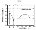
図2に、5.5MeVのエネルギーを持つアルファ粒子に対して行った実験によって得られた、炭化ケイ素放射線検出器の熱処理温度と電荷収集効率との関係をグラフと数値で示す。このグラフでは横軸に熱処理温度を、縦軸に電荷収集効率すなわち検出信号強度を示している。このときの熱処理時間は30分である。なお、30分以上の熱処理でも大きな変化はみられなかった。 FIG. 2 is a graph and a numerical diagram showing the relationship between the heat treatment temperature and the charge collection efficiency of the silicon carbide radiation detector, obtained by an experiment conducted on alpha particles having an energy of 5.5 MeV. In this graph, the horizontal axis indicates the heat treatment temperature, and the vertical axis indicates the charge collection efficiency, that is, the detection signal intensity. The heat treatment time at this time is 30 minutes. In addition, the big change was not seen even if it heat-processed for 30 minutes or more.
上述の加熱は、加熱温度を1℃毎に設定可能なアルバック理工社製の赤外線ランプ加熱処理装置を用いて行った。実験では、例えば、室温から100℃まで昇温させて熱処理した後、一度室温まで下げて電荷収集効率を測定した。次に、室温から150℃まで昇温させて熱処理した後、再度室温まで下げて電荷収集効率を測定した。このような方法で、50℃から400℃までの熱処理の影響について測定した。 The above-described heating was performed using an infrared lamp heat treatment apparatus manufactured by ULVAC-RIKO, which can set the heating temperature every 1 ° C. In the experiment, for example, the temperature was raised from room temperature to 100 ° C., heat treatment was performed, and then the temperature was once lowered to room temperature to measure the charge collection efficiency. Next, the temperature was raised from room temperature to 150 ° C. and heat-treated, and then the temperature was lowered again to room temperature to measure the charge collection efficiency. With such a method, the influence of heat treatment from 50 ° C. to 400 ° C. was measured.
図2の(a)のグラフから明らかなように、このグラフは200℃と350℃に屈曲点を有し、この範囲では電荷収集効率が初期値(100%)のほぼ90%以上に改善された。最適熱処理温度は300℃であり、このときの電荷収集効率は92.43%まで改善された。 As apparent from the graph of FIG. 2A, this graph has bending points at 200 ° C. and 350 ° C., and in this range, the charge collection efficiency is improved to almost 90% or more of the initial value (100%). It was. The optimum heat treatment temperature was 300 ° C., and the charge collection efficiency at this time was improved to 92.43%.
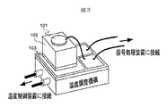
以上の実験データは、放射線であるアルファ粒子に長期間曝された炭化ケイ素結晶を、別の場所にある電気炉まで持って行って行った。しかし、実際には、炭化ケイ素放射線検出器と直接接触するようにして一体に形成され、通電電流の大きさに応じて温度制御が可能なヒータを備えた温度調整機構を用いることで、放射線検出器をその設置場所から取り外すことなく加熱処理することが可能である。そのような装置の一例を図3に示す。 The above experimental data was carried out by bringing a silicon carbide crystal that has been exposed to alpha particles as radiation for a long time to an electric furnace at another location. However, in reality, radiation detection is achieved by using a temperature adjustment mechanism that is integrally formed so as to be in direct contact with the silicon carbide radiation detector and has a heater that can control the temperature according to the magnitude of the energization current. Heat treatment can be performed without removing the vessel from its installation location. An example of such a device is shown in FIG.
また、4H-SiC炭化ケイ素結晶からなる放射線検出器の実使用運転において、炭化ケイ素放射線検出器が放射線に曝されることによって電荷収集効率がある程度低下した時点で、炭化ケイ素放射線検出器を200から350℃の範囲の温度で30分以上加熱して電荷収集効率を回復させることを繰り返すことで、炭化ケイ素放射線検出器を継続的に安定動作させることが可能となる。このとき、電荷収集効率が放射線曝露前の初期値の約20%以下になると、炭化ケイ素放射線検出器の動作が困難になるため、放射線検出器の実使用運転状態ならびに図2に示す実験データから、炭化ケイ素放射線検出器の電荷収集効率が放射線曝露前の初期値の80%以下、20%以上になった段階で、炭化ケイ素放射線検出器を200から350℃の範囲の温度で30分以上加熱することが好ましい。また、炭化ケイ素放射線検出器の運転休止時間を短縮する観点から、加熱時間は120分以下とすることが好ましい。 In actual operation of a radiation detector made of 4H-SiC silicon carbide crystal, when the silicon carbide radiation detector is exposed to radiation and the charge collection efficiency is reduced to some extent, the silicon carbide radiation detector is changed from 200 By repeating heating for 30 minutes or more at a temperature in the range of 350 ° C. to recover the charge collection efficiency, the silicon carbide radiation detector can be stably operated continuously. At this time, if the charge collection efficiency is about 20% or less of the initial value before exposure to radiation, the operation of the silicon carbide radiation detector becomes difficult. From the actual operating state of the radiation detector and the experimental data shown in FIG. When the charge collection efficiency of the silicon carbide radiation detector reaches 80% or less and 20% or more of the initial value before exposure to radiation, the silicon carbide radiation detector is heated at a temperature in the range of 200 to 350 ° C for 30 minutes or more. It is preferable to do. Further, from the viewpoint of shortening the operation stop time of the silicon carbide radiation detector, the heating time is preferably set to 120 minutes or less.
図3では、従来装置である温度制御装置や信号処理装置の詳細を示していない。実際には、信号処理装置において、電荷収集効率が初期値の80%以下(80%、70%など適宜しきい値を定める)になった時点で、温度制御装置に信号を送り、前述の手順に従って熱処理を開始するようにする。そして、温度を室温から昇温して行き、例えばSiC結晶の温度が300℃になった時点で、例えば30分間その温度を維持し、その後タイマーからの信号で温度を室温まで降下させて、再度放射線検出器としての使用を開始させる。 FIG. 3 does not show details of a temperature control device and a signal processing device, which are conventional devices. Actually, in the signal processing device, when the charge collection efficiency is 80% or less of the initial value (80%, 70%, etc., set the threshold appropriately), a signal is sent to the temperature control device, and the procedure described above To start heat treatment. Then, the temperature is raised from room temperature, for example, when the temperature of the SiC crystal reaches 300 ° C, for example, the temperature is maintained for 30 minutes, and then the temperature is lowered to room temperature with a signal from the timer, and then again. The use as a radiation detector is started.
11…電極
12…炭化ケイ素結晶
13…電極
DESCRIPTION OF SYMBOLS 11 ... Electrode 12 ... Silicon carbide crystal 13 ... Electrode
Claims (7)
前記所定の温度が200℃から350℃の範囲にある温度であり、前記所定の時間が30分以上であることを特徴とする炭化ケイ素放射線検出器の特性回復方法。 Restores the characteristics of the silicon carbide radiation detector that repairs the point defects generated in the silicon carbide crystal of the radiation detection part by heating the silicon carbide crystal at a predetermined temperature for a predetermined time. A method of
The method for recovering characteristics of a silicon carbide radiation detector, wherein the predetermined temperature is a temperature in a range of 200 ° C to 350 ° C, and the predetermined time is 30 minutes or more.
Priority Applications (1)
| Application Number | Priority Date | Filing Date | Title |
|---|---|---|---|
| JP2013015287A JP2014145705A (en) | 2013-01-30 | 2013-01-30 | Characteristic recovery method of silicon carbide radiation detector and operational method thereof |
Applications Claiming Priority (1)
| Application Number | Priority Date | Filing Date | Title |
|---|---|---|---|
| JP2013015287A JP2014145705A (en) | 2013-01-30 | 2013-01-30 | Characteristic recovery method of silicon carbide radiation detector and operational method thereof |
Publications (1)
| Publication Number | Publication Date |
|---|---|
| JP2014145705A true JP2014145705A (en) | 2014-08-14 |
Family
ID=51426061
Family Applications (1)
| Application Number | Title | Priority Date | Filing Date |
|---|---|---|---|
| JP2013015287A Pending JP2014145705A (en) | 2013-01-30 | 2013-01-30 | Characteristic recovery method of silicon carbide radiation detector and operational method thereof |
Country Status (1)
| Country | Link |
|---|---|
| JP (1) | JP2014145705A (en) |
Cited By (3)
| Publication number | Priority date | Publication date | Assignee | Title |
|---|---|---|---|---|
| WO2018207919A1 (en) * | 2017-05-12 | 2018-11-15 | 株式会社 東芝 | Photon counting-type radiation detector and radiological inspection device using same |
| CN114184618A (en) * | 2021-11-01 | 2022-03-15 | 山东睿芯半导体科技有限公司 | Silicon carbide crystal defect detection device |
| CN116387141A (en) * | 2023-06-07 | 2023-07-04 | 浙江大学杭州国际科创中心 | Preparation method of low-crack silicon carbide wafer and silicon carbide wafer |
Citations (4)
| Publication number | Priority date | Publication date | Assignee | Title |
|---|---|---|---|---|
| JPH04110691A (en) * | 1990-08-30 | 1992-04-13 | Shimadzu Corp | Radiation detector |
| JP2006295061A (en) * | 2005-04-14 | 2006-10-26 | Kansai Electric Power Co Inc:The | Bipolar semiconductor device, method for recovering forward voltage thereof, and method for reducing stacking fault |
| WO2009022378A1 (en) * | 2007-08-10 | 2009-02-19 | Osaka Electro-Communication University | Radiation detector |
| JP2009109216A (en) * | 2007-10-26 | 2009-05-21 | Hitachi Ltd | X-ray ct apparatus, and imaging method using x-ray ct apparatus |
-
2013
- 2013-01-30 JP JP2013015287A patent/JP2014145705A/en active Pending
Patent Citations (4)
| Publication number | Priority date | Publication date | Assignee | Title |
|---|---|---|---|---|
| JPH04110691A (en) * | 1990-08-30 | 1992-04-13 | Shimadzu Corp | Radiation detector |
| JP2006295061A (en) * | 2005-04-14 | 2006-10-26 | Kansai Electric Power Co Inc:The | Bipolar semiconductor device, method for recovering forward voltage thereof, and method for reducing stacking fault |
| WO2009022378A1 (en) * | 2007-08-10 | 2009-02-19 | Osaka Electro-Communication University | Radiation detector |
| JP2009109216A (en) * | 2007-10-26 | 2009-05-21 | Hitachi Ltd | X-ray ct apparatus, and imaging method using x-ray ct apparatus |
Non-Patent Citations (2)
| Title |
|---|
| FRANCESCO MOSCATELLI: "Silicon carbide for UV, alpha, beta and X-ray detectors:results and perspectives", RESMDD06 発表資料, JPN6017017264, December 2007 (2007-12-01), IT, ISSN: 0003707320 * |
| 岩本 直也: "炭化ケイ素PNダイオード高エネルギー粒子検出器の単一アルファ粒子誘起電荷収集特性に関する研究", 電気通信大学大学院 電気通信学研究科 博士(工学)学位申請論文, JPN6016041661, March 2012 (2012-03-01), JP, ISSN: 0003707319 * |
Cited By (8)
| Publication number | Priority date | Publication date | Assignee | Title |
|---|---|---|---|---|
| WO2018207919A1 (en) * | 2017-05-12 | 2018-11-15 | 株式会社 東芝 | Photon counting-type radiation detector and radiological inspection device using same |
| JPWO2018207919A1 (en) * | 2017-05-12 | 2020-03-12 | 株式会社東芝 | Photon counting type radiation detector and radiation inspection apparatus using the same |
| US10964836B2 (en) | 2017-05-12 | 2021-03-30 | Kabushiki Kaisha Toshiba | Photon counting-type radiation detector and radiological inspection device using same |
| JP7064485B2 (en) | 2017-05-12 | 2022-05-10 | 株式会社東芝 | Photon counting type radiation detector and radiation inspection equipment using it |
| CN114184618A (en) * | 2021-11-01 | 2022-03-15 | 山东睿芯半导体科技有限公司 | Silicon carbide crystal defect detection device |
| CN114184618B (en) * | 2021-11-01 | 2024-04-12 | 山东睿芯半导体科技有限公司 | Silicon carbide crystal defect detection device |
| CN116387141A (en) * | 2023-06-07 | 2023-07-04 | 浙江大学杭州国际科创中心 | Preparation method of low-crack silicon carbide wafer and silicon carbide wafer |
| CN116387141B (en) * | 2023-06-07 | 2023-10-13 | 浙江大学杭州国际科创中心 | Preparation method of low-crack silicon carbide wafer and silicon carbide wafer |
Similar Documents
| Publication | Publication Date | Title |
|---|---|---|
| Tarun et al. | Persistent photoconductivity in strontium titanate | |
| Hou et al. | Suppression of persistent photoconductivity in AlGaN/GaN ultraviolet photodetectors using in situ heating | |
| Zakeri et al. | On the preparation of clean tungsten single crystals | |
| Varney et al. | Energy levels of exciton traps in yttrium aluminum garnet single crystals | |
| JP2014145705A (en) | Characteristic recovery method of silicon carbide radiation detector and operational method thereof | |
| Dixit et al. | Effect of high dose γ-ray irradiation on GaAs pin photodetectors | |
| Kaminskii | Dynamics of the thermovoltaic effect in SmS | |
| Bruzzi et al. | Electrical properties and defect analysis of neutron irradiated undoped CVD diamond films | |
| JP6242718B2 (en) | Thermally stimulated current measuring device, thermally stimulated current measuring program, and thermally stimulated current measuring method | |
| Panahibakhsh et al. | Effect of XeCl laser irradiation on the defect structure of Nd: YAG crystals | |
| Marka et al. | Two-color optical technique for characterization of X-ray radiation-enhanced electron transport in SiO 2 | |
| Qiao et al. | Electrical characteristics of mid-wavelength HgCdTe photovoltaic detectors exposed to Gamma irradiation | |
| Kim et al. | Thermoluminescence from ultraviolet exposed MgAl2O4 | |
| Kajen et al. | Trap levels in graphene oxide: a thermally stimulated current study | |
| Liu et al. | Annealing effects and DLTS study on PNP silicon bipolar junction transistors irradiated by 20 MeV Br ions | |
| Bakhadyrkhanov et al. | Photoconductivity of silicon with nanoclusters of manganese atoms | |
| Tu et al. | TSC characteristics of AC aged ZnO varistors | |
| Chakravorty et al. | Luminescence from color centres induced by oxidation and ion irradiation in 4H–SiC | |
| Osmani et al. | Structural, topological, electrical and luminescence properties of CZ-silicon (CZ-Si) irradiated by neutrons | |
| Gu et al. | Correlated analysis of 2 MeV proton-induced radiation damage in CdZnTe crystals using photoluminescence and thermally stimulated current techniques | |
| Sciuto et al. | Reversibility of surface damage induced in SiC detectors by low intensity laser plasma | |
| Malo et al. | Ion bombardment induced surface electrical degradation monitoring by means of luminescence in aluminas | |
| Odrinskii | Photo-induced current transient spectroscopy of the ferroelectric-semiconductor TlGaSe 2 | |
| Løvlie et al. | Long range lateral migration of intrinsic point defects in n-type 4H-SiC | |
| RU2526216C1 (en) | Method to sort diamonds by electrophysical properties |
Legal Events
| Date | Code | Title | Description |
|---|---|---|---|
| A621 | Written request for application examination |
Free format text: JAPANESE INTERMEDIATE CODE: A621 Effective date: 20160119 |
|
| A521 | Request for written amendment filed |
Free format text: JAPANESE INTERMEDIATE CODE: A821 Effective date: 20160119 |
|
| A977 | Report on retrieval |
Free format text: JAPANESE INTERMEDIATE CODE: A971007 Effective date: 20161019 |
|
| A131 | Notification of reasons for refusal |
Free format text: JAPANESE INTERMEDIATE CODE: A131 Effective date: 20161101 |
|
| A711 | Notification of change in applicant |
Free format text: JAPANESE INTERMEDIATE CODE: A712 Effective date: 20161130 |
|
| A521 | Request for written amendment filed |
Free format text: JAPANESE INTERMEDIATE CODE: A523 Effective date: 20161228 |
|
| A521 | Request for written amendment filed |
Free format text: JAPANESE INTERMEDIATE CODE: A523 Effective date: 20170221 |
|
| RD02 | Notification of acceptance of power of attorney |
Free format text: JAPANESE INTERMEDIATE CODE: A7422 Effective date: 20170221 |
|
| A521 | Request for written amendment filed |
Free format text: JAPANESE INTERMEDIATE CODE: A821 Effective date: 20170222 |
|
| A131 | Notification of reasons for refusal |
Free format text: JAPANESE INTERMEDIATE CODE: A131 Effective date: 20170523 |
|
| A521 | Request for written amendment filed |
Free format text: JAPANESE INTERMEDIATE CODE: A523 Effective date: 20170720 |
|
| A02 | Decision of refusal |
Free format text: JAPANESE INTERMEDIATE CODE: A02 Effective date: 20180109 |