JP2014033104A - Heat radiation component and manufacturing method of the same - Google Patents
Heat radiation component and manufacturing method of the same Download PDFInfo
- Publication number
- JP2014033104A JP2014033104A JP2012173143A JP2012173143A JP2014033104A JP 2014033104 A JP2014033104 A JP 2014033104A JP 2012173143 A JP2012173143 A JP 2012173143A JP 2012173143 A JP2012173143 A JP 2012173143A JP 2014033104 A JP2014033104 A JP 2014033104A
- Authority
- JP
- Japan
- Prior art keywords
- carbon
- plating layer
- carbon nanotubes
- carbon material
- base material
- Prior art date
- Legal status (The legal status is an assumption and is not a legal conclusion. Google has not performed a legal analysis and makes no representation as to the accuracy of the status listed.)
- Pending
Links
- 230000005855 radiation Effects 0.000 title claims abstract description 22
- 238000004519 manufacturing process Methods 0.000 title claims abstract description 17
- OKTJSMMVPCPJKN-UHFFFAOYSA-N Carbon Chemical compound [C] OKTJSMMVPCPJKN-UHFFFAOYSA-N 0.000 claims abstract description 96
- 239000002041 carbon nanotube Substances 0.000 claims abstract description 94
- 229910021393 carbon nanotube Inorganic materials 0.000 claims abstract description 94
- 238000007747 plating Methods 0.000 claims abstract description 72
- 239000000463 material Substances 0.000 claims abstract description 69
- 239000003575 carbonaceous material Substances 0.000 claims abstract description 46
- 230000017525 heat dissipation Effects 0.000 claims description 32
- 238000000034 method Methods 0.000 claims description 29
- 239000000758 substrate Substances 0.000 claims description 26
- PXHVJJICTQNCMI-UHFFFAOYSA-N Nickel Chemical compound [Ni] PXHVJJICTQNCMI-UHFFFAOYSA-N 0.000 claims description 14
- 238000005229 chemical vapour deposition Methods 0.000 claims description 8
- 229910052759 nickel Inorganic materials 0.000 claims description 5
- 238000009713 electroplating Methods 0.000 description 24
- 229910052751 metal Inorganic materials 0.000 description 13
- 239000002184 metal Substances 0.000 description 13
- 239000010949 copper Substances 0.000 description 12
- 238000007772 electroless plating Methods 0.000 description 8
- 229910052802 copper Inorganic materials 0.000 description 7
- KDLHZDBZIXYQEI-UHFFFAOYSA-N Palladium Chemical compound [Pd] KDLHZDBZIXYQEI-UHFFFAOYSA-N 0.000 description 6
- -1 for example Substances 0.000 description 6
- 239000004065 semiconductor Substances 0.000 description 6
- RYGMFSIKBFXOCR-UHFFFAOYSA-N Copper Chemical compound [Cu] RYGMFSIKBFXOCR-UHFFFAOYSA-N 0.000 description 5
- 230000000052 comparative effect Effects 0.000 description 5
- 150000001875 compounds Chemical class 0.000 description 5
- 238000012986 modification Methods 0.000 description 5
- 230000004048 modification Effects 0.000 description 5
- 239000003054 catalyst Substances 0.000 description 4
- 239000010931 gold Substances 0.000 description 4
- XEEYBQQBJWHFJM-UHFFFAOYSA-N Iron Chemical compound [Fe] XEEYBQQBJWHFJM-UHFFFAOYSA-N 0.000 description 3
- 229910017052 cobalt Inorganic materials 0.000 description 3
- 239000010941 cobalt Substances 0.000 description 3
- GUTLYIVDDKVIGB-UHFFFAOYSA-N cobalt atom Chemical compound [Co] GUTLYIVDDKVIGB-UHFFFAOYSA-N 0.000 description 3
- 238000010586 diagram Methods 0.000 description 3
- 230000000694 effects Effects 0.000 description 3
- 239000007789 gas Substances 0.000 description 3
- 238000010438 heat treatment Methods 0.000 description 3
- 125000006353 oxyethylene group Chemical group 0.000 description 3
- XKRFYHLGVUSROY-UHFFFAOYSA-N Argon Chemical compound [Ar] XKRFYHLGVUSROY-UHFFFAOYSA-N 0.000 description 2
- 229910018104 Ni-P Inorganic materials 0.000 description 2
- 229910018536 Ni—P Inorganic materials 0.000 description 2
- BQCADISMDOOEFD-UHFFFAOYSA-N Silver Chemical compound [Ag] BQCADISMDOOEFD-UHFFFAOYSA-N 0.000 description 2
- 239000000956 alloy Substances 0.000 description 2
- 229910045601 alloy Inorganic materials 0.000 description 2
- 229910052782 aluminium Inorganic materials 0.000 description 2
- XAGFODPZIPBFFR-UHFFFAOYSA-N aluminium Chemical compound [Al] XAGFODPZIPBFFR-UHFFFAOYSA-N 0.000 description 2
- 239000002270 dispersing agent Substances 0.000 description 2
- 239000000835 fiber Substances 0.000 description 2
- PCHJSUWPFVWCPO-UHFFFAOYSA-N gold Chemical compound [Au] PCHJSUWPFVWCPO-UHFFFAOYSA-N 0.000 description 2
- 229910052737 gold Inorganic materials 0.000 description 2
- 239000002071 nanotube Substances 0.000 description 2
- 229910052763 palladium Inorganic materials 0.000 description 2
- 229910052709 silver Inorganic materials 0.000 description 2
- 239000004332 silver Substances 0.000 description 2
- 125000003903 2-propenyl group Chemical group [H]C([*])([H])C([H])=C([H])[H] 0.000 description 1
- CFNMUZCFSDMZPQ-GHXNOFRVSA-N 7-[(z)-3-methyl-4-(4-methyl-5-oxo-2h-furan-2-yl)but-2-enoxy]chromen-2-one Chemical compound C=1C=C2C=CC(=O)OC2=CC=1OC/C=C(/C)CC1OC(=O)C(C)=C1 CFNMUZCFSDMZPQ-GHXNOFRVSA-N 0.000 description 1
- HGINCPLSRVDWNT-UHFFFAOYSA-N Acrolein Chemical compound C=CC=O HGINCPLSRVDWNT-UHFFFAOYSA-N 0.000 description 1
- UFHFLCQGNIYNRP-UHFFFAOYSA-N Hydrogen Chemical compound [H][H] UFHFLCQGNIYNRP-UHFFFAOYSA-N 0.000 description 1
- 229920002125 Sokalan® Polymers 0.000 description 1
- 150000000475 acetylene derivatives Chemical class 0.000 description 1
- 125000003172 aldehyde group Chemical group 0.000 description 1
- HSFWRNGVRCDJHI-UHFFFAOYSA-N alpha-acetylene Natural products C#C HSFWRNGVRCDJHI-UHFFFAOYSA-N 0.000 description 1
- 229910052786 argon Inorganic materials 0.000 description 1
- 229910052799 carbon Inorganic materials 0.000 description 1
- 239000006229 carbon black Substances 0.000 description 1
- 239000002134 carbon nanofiber Substances 0.000 description 1
- 125000002843 carboxylic acid group Chemical group 0.000 description 1
- 239000012159 carrier gas Substances 0.000 description 1
- 238000012790 confirmation Methods 0.000 description 1
- 238000007796 conventional method Methods 0.000 description 1
- 239000006185 dispersion Substances 0.000 description 1
- 230000005684 electric field Effects 0.000 description 1
- 150000002148 esters Chemical class 0.000 description 1
- 125000005677 ethinylene group Chemical group [*:2]C#C[*:1] 0.000 description 1
- 229910002804 graphite Inorganic materials 0.000 description 1
- 239000010439 graphite Substances 0.000 description 1
- 125000000468 ketone group Chemical group 0.000 description 1
- VNWKTOKETHGBQD-UHFFFAOYSA-N methane Chemical compound C VNWKTOKETHGBQD-UHFFFAOYSA-N 0.000 description 1
- 239000000203 mixture Substances 0.000 description 1
- 150000002894 organic compounds Chemical class 0.000 description 1
- 239000004584 polyacrylic acid Substances 0.000 description 1
- 238000012545 processing Methods 0.000 description 1
- 229940070891 pyridium Drugs 0.000 description 1
- 238000004544 sputter deposition Methods 0.000 description 1
- 238000003756 stirring Methods 0.000 description 1
- 238000006467 substitution reaction Methods 0.000 description 1
- 239000004094 surface-active agent Substances 0.000 description 1
Images


Classifications
-
- C—CHEMISTRY; METALLURGY
- C25—ELECTROLYTIC OR ELECTROPHORETIC PROCESSES; APPARATUS THEREFOR
- C25D—PROCESSES FOR THE ELECTROLYTIC OR ELECTROPHORETIC PRODUCTION OF COATINGS; ELECTROFORMING; APPARATUS THEREFOR
- C25D5/00—Electroplating characterised by the process; Pretreatment or after-treatment of workpieces
- C25D5/007—Electroplating using magnetic fields, e.g. magnets
- C25D5/009—Deposition of ferromagnetic material
-
- C—CHEMISTRY; METALLURGY
- C01—INORGANIC CHEMISTRY
- C01B—NON-METALLIC ELEMENTS; COMPOUNDS THEREOF; METALLOIDS OR COMPOUNDS THEREOF NOT COVERED BY SUBCLASS C01C
- C01B32/00—Carbon; Compounds thereof
- C01B32/15—Nano-sized carbon materials
- C01B32/158—Carbon nanotubes
- C01B32/16—Preparation
-
- C—CHEMISTRY; METALLURGY
- C23—COATING METALLIC MATERIAL; COATING MATERIAL WITH METALLIC MATERIAL; CHEMICAL SURFACE TREATMENT; DIFFUSION TREATMENT OF METALLIC MATERIAL; COATING BY VACUUM EVAPORATION, BY SPUTTERING, BY ION IMPLANTATION OR BY CHEMICAL VAPOUR DEPOSITION, IN GENERAL; INHIBITING CORROSION OF METALLIC MATERIAL OR INCRUSTATION IN GENERAL
- C23C—COATING METALLIC MATERIAL; COATING MATERIAL WITH METALLIC MATERIAL; SURFACE TREATMENT OF METALLIC MATERIAL BY DIFFUSION INTO THE SURFACE, BY CHEMICAL CONVERSION OR SUBSTITUTION; COATING BY VACUUM EVAPORATION, BY SPUTTERING, BY ION IMPLANTATION OR BY CHEMICAL VAPOUR DEPOSITION, IN GENERAL
- C23C18/00—Chemical coating by decomposition of either liquid compounds or solutions of the coating forming compounds, without leaving reaction products of surface material in the coating; Contact plating
- C23C18/16—Chemical coating by decomposition of either liquid compounds or solutions of the coating forming compounds, without leaving reaction products of surface material in the coating; Contact plating by reduction or substitution, e.g. electroless plating
- C23C18/1601—Process or apparatus
- C23C18/1633—Process of electroless plating
- C23C18/1646—Characteristics of the product obtained
- C23C18/165—Multilayered product
-
- C—CHEMISTRY; METALLURGY
- C23—COATING METALLIC MATERIAL; COATING MATERIAL WITH METALLIC MATERIAL; CHEMICAL SURFACE TREATMENT; DIFFUSION TREATMENT OF METALLIC MATERIAL; COATING BY VACUUM EVAPORATION, BY SPUTTERING, BY ION IMPLANTATION OR BY CHEMICAL VAPOUR DEPOSITION, IN GENERAL; INHIBITING CORROSION OF METALLIC MATERIAL OR INCRUSTATION IN GENERAL
- C23C—COATING METALLIC MATERIAL; COATING MATERIAL WITH METALLIC MATERIAL; SURFACE TREATMENT OF METALLIC MATERIAL BY DIFFUSION INTO THE SURFACE, BY CHEMICAL CONVERSION OR SUBSTITUTION; COATING BY VACUUM EVAPORATION, BY SPUTTERING, BY ION IMPLANTATION OR BY CHEMICAL VAPOUR DEPOSITION, IN GENERAL
- C23C18/00—Chemical coating by decomposition of either liquid compounds or solutions of the coating forming compounds, without leaving reaction products of surface material in the coating; Contact plating
- C23C18/16—Chemical coating by decomposition of either liquid compounds or solutions of the coating forming compounds, without leaving reaction products of surface material in the coating; Contact plating by reduction or substitution, e.g. electroless plating
- C23C18/1601—Process or apparatus
- C23C18/1633—Process of electroless plating
- C23C18/1655—Process features
- C23C18/1662—Use of incorporated material in the solution or dispersion, e.g. particles, whiskers, wires
-
- C—CHEMISTRY; METALLURGY
- C23—COATING METALLIC MATERIAL; COATING MATERIAL WITH METALLIC MATERIAL; CHEMICAL SURFACE TREATMENT; DIFFUSION TREATMENT OF METALLIC MATERIAL; COATING BY VACUUM EVAPORATION, BY SPUTTERING, BY ION IMPLANTATION OR BY CHEMICAL VAPOUR DEPOSITION, IN GENERAL; INHIBITING CORROSION OF METALLIC MATERIAL OR INCRUSTATION IN GENERAL
- C23C—COATING METALLIC MATERIAL; COATING MATERIAL WITH METALLIC MATERIAL; SURFACE TREATMENT OF METALLIC MATERIAL BY DIFFUSION INTO THE SURFACE, BY CHEMICAL CONVERSION OR SUBSTITUTION; COATING BY VACUUM EVAPORATION, BY SPUTTERING, BY ION IMPLANTATION OR BY CHEMICAL VAPOUR DEPOSITION, IN GENERAL
- C23C18/00—Chemical coating by decomposition of either liquid compounds or solutions of the coating forming compounds, without leaving reaction products of surface material in the coating; Contact plating
- C23C18/16—Chemical coating by decomposition of either liquid compounds or solutions of the coating forming compounds, without leaving reaction products of surface material in the coating; Contact plating by reduction or substitution, e.g. electroless plating
- C23C18/1601—Process or apparatus
- C23C18/1633—Process of electroless plating
- C23C18/1655—Process features
- C23C18/1664—Process features with additional means during the plating process
- C23C18/1673—Magnetic field
-
- C—CHEMISTRY; METALLURGY
- C25—ELECTROLYTIC OR ELECTROPHORETIC PROCESSES; APPARATUS THEREFOR
- C25D—PROCESSES FOR THE ELECTROLYTIC OR ELECTROPHORETIC PRODUCTION OF COATINGS; ELECTROFORMING; APPARATUS THEREFOR
- C25D15/00—Electrolytic or electrophoretic production of coatings containing embedded materials, e.g. particles, whiskers, wires
-
- C—CHEMISTRY; METALLURGY
- C25—ELECTROLYTIC OR ELECTROPHORETIC PROCESSES; APPARATUS THEREFOR
- C25D—PROCESSES FOR THE ELECTROLYTIC OR ELECTROPHORETIC PRODUCTION OF COATINGS; ELECTROFORMING; APPARATUS THEREFOR
- C25D5/00—Electroplating characterised by the process; Pretreatment or after-treatment of workpieces
- C25D5/007—Electroplating using magnetic fields, e.g. magnets
-
- F—MECHANICAL ENGINEERING; LIGHTING; HEATING; WEAPONS; BLASTING
- F28—HEAT EXCHANGE IN GENERAL
- F28F—DETAILS OF HEAT-EXCHANGE AND HEAT-TRANSFER APPARATUS, OF GENERAL APPLICATION
- F28F3/00—Plate-like or laminated elements; Assemblies of plate-like or laminated elements
-
- H—ELECTRICITY
- H01—ELECTRIC ELEMENTS
- H01L—SEMICONDUCTOR DEVICES NOT COVERED BY CLASS H10
- H01L23/00—Details of semiconductor or other solid state devices
- H01L23/34—Arrangements for cooling, heating, ventilating or temperature compensation ; Temperature sensing arrangements
- H01L23/36—Selection of materials, or shaping, to facilitate cooling or heating, e.g. heatsinks
- H01L23/373—Cooling facilitated by selection of materials for the device or materials for thermal expansion adaptation, e.g. carbon
- H01L23/3736—Metallic materials
-
- B—PERFORMING OPERATIONS; TRANSPORTING
- B82—NANOTECHNOLOGY
- B82Y—SPECIFIC USES OR APPLICATIONS OF NANOSTRUCTURES; MEASUREMENT OR ANALYSIS OF NANOSTRUCTURES; MANUFACTURE OR TREATMENT OF NANOSTRUCTURES
- B82Y30/00—Nanotechnology for materials or surface science, e.g. nanocomposites
-
- B—PERFORMING OPERATIONS; TRANSPORTING
- B82—NANOTECHNOLOGY
- B82Y—SPECIFIC USES OR APPLICATIONS OF NANOSTRUCTURES; MEASUREMENT OR ANALYSIS OF NANOSTRUCTURES; MANUFACTURE OR TREATMENT OF NANOSTRUCTURES
- B82Y40/00—Manufacture or treatment of nanostructures
-
- C—CHEMISTRY; METALLURGY
- C01—INORGANIC CHEMISTRY
- C01B—NON-METALLIC ELEMENTS; COMPOUNDS THEREOF; METALLOIDS OR COMPOUNDS THEREOF NOT COVERED BY SUBCLASS C01C
- C01B2202/00—Structure or properties of carbon nanotubes
- C01B2202/20—Nanotubes characterized by their properties
- C01B2202/34—Length
-
- C—CHEMISTRY; METALLURGY
- C01—INORGANIC CHEMISTRY
- C01B—NON-METALLIC ELEMENTS; COMPOUNDS THEREOF; METALLOIDS OR COMPOUNDS THEREOF NOT COVERED BY SUBCLASS C01C
- C01B2202/00—Structure or properties of carbon nanotubes
- C01B2202/20—Nanotubes characterized by their properties
- C01B2202/36—Diameter
-
- F—MECHANICAL ENGINEERING; LIGHTING; HEATING; WEAPONS; BLASTING
- F28—HEAT EXCHANGE IN GENERAL
- F28F—DETAILS OF HEAT-EXCHANGE AND HEAT-TRANSFER APPARATUS, OF GENERAL APPLICATION
- F28F21/00—Constructions of heat-exchange apparatus characterised by the selection of particular materials
- F28F21/02—Constructions of heat-exchange apparatus characterised by the selection of particular materials of carbon, e.g. graphite
-
- F—MECHANICAL ENGINEERING; LIGHTING; HEATING; WEAPONS; BLASTING
- F28—HEAT EXCHANGE IN GENERAL
- F28F—DETAILS OF HEAT-EXCHANGE AND HEAT-TRANSFER APPARATUS, OF GENERAL APPLICATION
- F28F3/00—Plate-like or laminated elements; Assemblies of plate-like or laminated elements
- F28F3/02—Elements or assemblies thereof with means for increasing heat-transfer area, e.g. with fins, with recesses, with corrugations
-
- H—ELECTRICITY
- H01—ELECTRIC ELEMENTS
- H01L—SEMICONDUCTOR DEVICES NOT COVERED BY CLASS H10
- H01L2924/00—Indexing scheme for arrangements or methods for connecting or disconnecting semiconductor or solid-state bodies as covered by H01L24/00
- H01L2924/0001—Technical content checked by a classifier
- H01L2924/0002—Not covered by any one of groups H01L24/00, H01L24/00 and H01L2224/00
Abstract
Description
本発明は、放熱部品及びその製造方法に関する。 The present invention relates to a heat dissipation component and a method for manufacturing the same.
CPU(Central Processing Unit)等に使用される半導体素子は動作時に高温となるため、その熱を速やかに外部に放熱することは、半導体素子の性能を発揮する上で極めて重要である。 A semiconductor element used in a CPU (Central Processing Unit) or the like has a high temperature during operation. Therefore, it is extremely important to quickly dissipate the heat to the outside in order to exhibit the performance of the semiconductor element.
そこで、従来より、半導体素子上にヒートスプレッダやヒートパイプ等の放熱部品を装着して、半導体素子が発する熱を外部に有効に放出する経路を確保することが行われている。又、ヒートスプレッダやヒートパイプ等の放熱部品の放熱性能(熱放射性)を向上する検討が行われている。例えば、ヒートスプレッダやヒートパイプ等の放熱部品の表面にカーボンナノチューブ等の炭素材料が分散された金属層を形成することにより、放熱部品の放熱性能(熱放射性)を向上する試みがなされている。 Therefore, conventionally, a heat dissipation component such as a heat spreader or a heat pipe is mounted on the semiconductor element to ensure a path for effectively releasing the heat generated by the semiconductor element to the outside. Further, studies are being made to improve the heat radiation performance (heat radiation) of heat radiation components such as heat spreaders and heat pipes. For example, an attempt has been made to improve the heat dissipation performance (thermal radiation) of a heat dissipation component by forming a metal layer in which a carbon material such as carbon nanotube is dispersed on the surface of a heat dissipation component such as a heat spreader or a heat pipe.
カーボンナノチューブ等の炭素材料を金属層中に分散する技術としては、例えば、以下の技術を挙げることができる。第1の技術としては、カーボンナノチューブの繊維長よりも細い孔に、カーボンナノチューブを含むめっき液を入り込ませることにより、カーボンナノチューブを垂直に近い方向に配向させようとする技術である(例えば、特許文献1参照)。第2の技術としては、電気めっきによって金属めっき層を形成する際に、電気力線に沿ってカーボンナノチューブを垂直方向に配向させようとする技術である(例えば、特許文献2参照)。 Examples of techniques for dispersing a carbon material such as carbon nanotubes in a metal layer include the following techniques. The first technique is a technique for orienting carbon nanotubes in a nearly vertical direction by allowing a plating solution containing carbon nanotubes to enter holes that are narrower than the fiber length of carbon nanotubes (for example, patents). Reference 1). The second technique is a technique for orienting carbon nanotubes in the vertical direction along the lines of electric force when forming a metal plating layer by electroplating (see, for example, Patent Document 2).
しかしながら、上記第1の技術では、カーボンナノチューブのうちの一部は垂直方向に配向するかもしれないが、多くのカーボンナノチューブは孔に対して斜めに配向する。又、上記第2の技術では、電気めっきの電気力線ではパワーが不十分であるため、垂直方向に配向するカーボンナノチューブの割合をある程度上げることはできるとしても、なお多くのカーボンナノチューブは斜めに配向する。このように、従来知られていた技術では、カーボンナノチューブ等の炭素材料を全体的に垂直方向に配向させることは困難であった。 However, in the first technique, some of the carbon nanotubes may be oriented in the vertical direction, but many carbon nanotubes are oriented obliquely with respect to the holes. In the second technique, the electric field lines of electroplating have insufficient power, so even if the proportion of carbon nanotubes oriented in the vertical direction can be increased to some extent, many carbon nanotubes are still oblique. Orient. As described above, it has been difficult for conventional techniques to orient carbon materials such as carbon nanotubes in the vertical direction as a whole.
本発明は、上記の点に鑑みてなされたものであり、カーボンナノチューブ等の炭素材料を垂直方向に配向させた放熱部品及びその製造方法を提供することを課題とする。 This invention is made | formed in view of said point, and makes it a subject to provide the thermal radiation component which orientated carbon materials, such as a carbon nanotube, to the orthogonal | vertical direction, and its manufacturing method.
本放熱部品は、基材と、前記基材の所定の面に対して垂直な方向に配向された炭素材料と、前記炭素材料の間隙に充填されためっき層と、を有し、前記炭素材料の一部が前記めっき層の表面から前記基材とは反対側に突出していることを要件とする。 The heat dissipation component includes a base material, a carbon material oriented in a direction perpendicular to a predetermined surface of the base material, and a plating layer filled in a gap between the carbon materials, and the carbon material Is required to protrude from the surface of the plating layer to the side opposite to the substrate.
本放熱部品の製造方法の一の形態は、基材の所定の面に、化学的気相成長法により、前記所定の面に対して垂直な方向に配向された炭素材料を形成する工程と、前記炭素材料の間隙を充填し、前記炭素材料の一部が前記基材とは反対側に突出するようにめっき層を形成する工程と、を有することを要件とする。 One aspect of the method for manufacturing the heat dissipation component is a step of forming a carbon material oriented in a direction perpendicular to the predetermined surface by chemical vapor deposition on a predetermined surface of the base material; And filling a gap between the carbon materials, and forming a plating layer so that a part of the carbon material protrudes on the opposite side of the base material.
本放熱部品の製造方法の他の形態は、基材の所定の面に垂直な方向に磁場を印加する工程と、めっき層を形成する材料中に炭素材料が分散されためっき液を用いて、前記磁場中において前記所定の面にめっきを施す工程と、を有し、前記めっきを施す工程では、前記炭素材料が前記所定の面に対して垂直な方向に配向され、前記炭素材料の間隙を充填し前記炭素材料の一部が前記基材とは反対側に突出するように前記めっき層を形成することを要件とする。 Other forms of the manufacturing method of the heat dissipation component include a step of applying a magnetic field in a direction perpendicular to a predetermined surface of the substrate, and a plating solution in which a carbon material is dispersed in a material for forming a plating layer. Plating the predetermined surface in the magnetic field, and in the plating step, the carbon material is oriented in a direction perpendicular to the predetermined surface, and a gap between the carbon material is formed. It is necessary to form the plating layer so that a part of the carbon material is filled and protrudes on the opposite side of the base material.
本発明によれば、カーボンナノチューブ等の炭素材料を垂直方向に配向させた放熱部品及びその製造方法を提供できる。 ADVANTAGE OF THE INVENTION According to this invention, the heat radiating component which orientated carbon materials, such as a carbon nanotube, to the orthogonal | vertical direction, and its manufacturing method can be provided.
以下、図面を参照して発明を実施するための形態について説明する。なお、各図面において、同一構成部分には同一符号を付し、重複した説明を省略する場合がある。 Hereinafter, embodiments for carrying out the invention will be described with reference to the drawings. In addition, in each drawing, the same code | symbol is attached | subjected to the same component and the overlapping description may be abbreviate | omitted.
〈第1の実施の形態〉
[第1の実施の形態に係る放熱部品の構造]
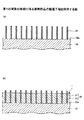
まず、第1の実施の形態に係る放熱部品の構造について説明する。図1は、第1の実施の形態に係る放熱部品を例示する断面模式図である。図1を参照するに、放熱部品1は、基材10と、炭素材料含有層20とを有する。
<First Embodiment>
[Structure of heat dissipation component according to the first embodiment]
First, the structure of the heat dissipation component according to the first embodiment will be described. FIG. 1 is a schematic cross-sectional view illustrating a heat dissipation component according to the first embodiment. Referring to FIG. 1, the
基材10は、熱伝導率が良好な金属から構成することが好ましく、具体的には、例えば、銅(Cu)、アルミニウム(Al)、鉄(Fe)、又はこれらの合金等を用いることができる。但し、基材10は、熱伝導率が良好な材料であれば、金属以外の材料から形成してもよい。
The
炭素材料含有層20は、基材10の面10aに形成されためっき層22中にカーボンナノチューブ21が含有された層である。めっき層22は、カーボンナノチューブ21の間隙に充填されている。めっき層22の厚さTは、例えば、50μm程度とすることができる。カーボンナノチューブ21は、基材10の面10aに対して垂直な方向に配向されており、カーボンナノチューブ21の一部がめっき層22の表面から基材10とは反対側に突出している。
The carbon material-containing
なお、本願において、垂直とは、カーボンナノチューブ21が基材10の面10aに対して完全に垂直である場合のみではなく、本願の効果を損なわない範囲内で基材10の面10aに対しておおよそ垂直である場合も含むものとする。
In the present application, the term “perpendicular” refers not only to the case where the
以降、カーボンナノチューブ21のめっき層22の表面から突出している部分を、カーボンナノチューブ21の突出部と称する場合がある。カーボンナノチューブ21の突出部のめっき層22の表面からの突出量Lは、例えば、5〜10μm程度とすることができる。なお、突出量Lは、カーボンナノチューブ21ごとに異なっていてもよい。カーボンナノチューブ21の突出部の投影面積は、めっき層22の表面に対して3%以上とすることができる。
Hereinafter, the portion of the
なお、突出量Lが5μmよりも小さいと放熱性能が低下するため好ましくない。又、突出量Lが10μmよりも大きいとカーボンナノチューブ21が折れたりめっき層22から抜けたりするため好ましくない。
In addition, since the thermal radiation performance will fall when protrusion amount L is smaller than 5 micrometers, it is unpreferable. On the other hand, if the protruding amount L is larger than 10 μm, the
カーボンナノチューブ21の径は、例えば、100〜300nm程度とすることができる。カーボンナノチューブ21の長さは、例えば、55〜60μm程度とすることができる。例えば、数万本程度のカーボンナノチューブ21が、基材10の面10aに林立している。なお、カーボンナノチューブ21は、本発明に係る線状の材料の代表的な一例である。
The diameter of the
めっき層22は、熱伝導率が良好で錆び難い金属から構成することが好ましく、具体的には、例えば、ニッケル(Ni)、銅(Cu)、コバルト(Co)、金(Au)、銀(Ag)、パラジウム(Pd)等を用いることができる。
The
なお、カーボンナノチューブ21に代えて、カーボンナノファイバ、グラファイト、カーボンブラック等の炭素材料を用いても構わない。又、これらの炭素材料が混合したものを用いても構わない。
In place of the
放熱部品1は、例えば、ベーパーチャンバー、ヒートパイプ、ヒートスプレッダ、発光ダイオード(LED)の筺体等に適用することができる。つまり、放熱部品1の基材10は半導体素子等の発熱体に取り付けられ、半導体素子等の発する熱を基材10を介して炭素材料含有層20の表面に迅速に伝達する。
The
[第1の実施の形態に係る放熱部品の製造方法]
次に、第1の実施の形態に係る放熱部品の製造方法について説明する。図2は、第1の実施の形態に係る放熱部品の製造工程を例示する図である。まず、図2(a)に示す工程では、基材10を準備し、基材10の面10aに対して垂直な方向にカーボンナノチューブ21を林立するように形成する。
[Manufacturing Method of Heat Dissipating Component According to First Embodiment]
Next, a method for manufacturing a heat dissipation component according to the first embodiment will be described. FIG. 2 is a diagram illustrating a manufacturing process of the heat dissipating component according to the first embodiment. First, in the process illustrated in FIG. 2A, the
基材10は、熱伝導率が良好な金属から構成することが好ましく、具体的には、例えば、銅(Cu)、アルミニウム(Al)、鉄(Fe)、又はこれらの合金等を用いることができる。但し、基材10は、熱伝導率が良好な材料であれば、金属以外の材料から形成してもよい。
The
カーボンナノチューブ21は、CVD法(化学的気相成長法)により、基材10の面10aに対して垂直な方向に林立するように、基材10の面10aに直接形成できる。より具体的には、基材10を所定の圧力及び温度に調整された加熱炉に入れて、CVD法(化学的気相成長法)により、基材10の面10aにカーボンナノチューブ21を形成する。加熱炉の圧力及び温度は、例えば、100pa及び600℃程度とすることができる。又、プロセスガスとしては、例えば、アセチレンガス等を用いることができ、キャリアガスとしては、例えば、アルゴンガスや水素ガス等を用いることができる。
The
これにより、基材10の面10aに、多数のカーボンナノチューブ21が、基材10の面10aに対して垂直な方向に形成される。なお、各カーボンナノチューブ21の一端は、基材10の面10aに接している。
Thereby, a large number of
カーボンナノチューブ21の径は、例えば、100〜300nm程度とすることができる。カーボンナノチューブ21の長さは、例えば、55〜60μm程度とすることができる。カーボンナノチューブ21の本数は、例えば、数万本程度とすることができる。なお、カーボンナノチューブ21の長さ(基材10の面10aからカーボンナノチューブ21の先端部までの長さ)は、カーボンナノチューブ21の成長時間によって制御できる。
The diameter of the
なお、基材10として金属以外の材料を用いる場合には、基材10の面10aにスパッタリング法等により金属触媒層を形成し、金属触媒層上にCVD法(化学的気相成長法)によりカーボンナノチューブ21を形成すればよい。金属触媒層としては、例えば、鉄(Fe)、コバルト(Co)、ニッケル(Ni)等を用いることができる。金属触媒層の厚さは、例えば、数nm程度とすることができる。
In addition, when using materials other than a metal as the
次に、図2(b)に示す工程では、基材10の面10aにめっき層22を形成し、めっき層22中にカーボンナノチューブ21が含有された炭素材料含有層20を作製する。つまり、カーボンナノチューブ21の間隙を充填し、カーボンナノチューブ21の一部が基材10とは反対側に突出するようにめっき層22を形成する。この工程により、放熱部品1が完成する。
Next, in the step shown in FIG. 2B, the
本実施の形態では、基材10を給電層として利用する電解めっき法により、基材10の面10aにめっき層22を形成する。めっき層22は、各カーボンナノチューブ21の一部がめっき層22の表面から基材10とは反対側に突出するように形成する。めっき層22の厚さは、例えば、50μm程度とすることができる。
In the present embodiment, the
カーボンナノチューブ21の突出部のめっき層22の表面からの突出量は、例えば、5〜10μm程度とすることができる。なお、カーボンナノチューブ21の突出部のめっき層22の表面からの突出量は、カーボンナノチューブ21ごとに異なっていてもよい。カーボンナノチューブ21の突出部の投影面積は、めっき層22の表面に対して3%以上とすることができる。
The protruding amount of the protruding portion of the
以上のように、第1の実施の形態に係る放熱部品1では、カーボンナノチューブ21の一部がめっき層22の表面から基材10とは反対側に突出している。そのため、カーボンナノチューブ21の突出部からは、基材10から伝熱された熱が直ちに放熱され、炭素材料含有層20の熱放射性を向上できる。
As described above, in the
又、各カーボンナノチューブ21は、基材10の面10aに対して垂直な方向に配向されているため、各カーボンナノチューブ21の有する繊維長方向(長軸方向)の特性を十分生かすことができ、炭素材料含有層20の熱放射性を更に向上できる。
In addition, since each
〈第1の実施の形態の変形例〉
第1の実施の形態では、めっき層22を電解めっき法により形成する例を示したが、めっき層22は無電解めっき法により形成してもよい。
<Modification of First Embodiment>
In the first embodiment, the example in which the
無電解めっき法によりめっき層22を形成するには、図2(a)と同様の工程を実行後、図2(b)に示す工程において、電解めっきに代えて無電解めっきを実行すればよい。無電解めっき法により形成するめっき層22の材料としては、例えば、Ni−P、Ni−B、Cu等を用いることができる。このように、無電解めっき法によりめっき層22を形成しても第1の実施の形態と同様の効果を奏する。
In order to form the
〈第2の実施の形態〉
第2の実施の形態では、第1の実施の形態とは異なる方法により放熱部品1を作製する例を示す。なお、第2の実施の形態において、第1の実施の形態と共通する部分についての説明は省略する。
<Second Embodiment>
In 2nd Embodiment, the example which produces the
図3は、第2の実施の形態に係る放熱部品の製造工程を例示する図である。まず、図3(a)に示す工程では、基材10を準備し、準備した基材10を磁場発生装置(図示せず)内に配置し、磁場発生装置を起動して面10aに対して垂直な方向に磁場Mを発生させる。磁場発生装置としては、例えば、超伝導マグネットを用いた装置を使用できる。発生する磁場Mは、例えば、5〜10テスラ程度とすることができる。なお、基材10の材料等は、第1の実施の形態と同様とすることができる。
FIG. 3 is a diagram illustrating a manufacturing process of the heat dissipating component according to the second embodiment. First, in the process shown in FIG. 3A, the
次に、図3(b)に示す工程では、めっき層22中にカーボンナノチューブ21が含有された炭素材料含有層20を形成する。つまり、カーボンナノチューブ21が面10aに対して垂直な方向に配向され、カーボンナノチューブ21の間隙を充填しカーボンナノチューブ21の一部が基材10とは反対側に突出するようにめっき層22を形成する。
Next, in the step shown in FIG. 3B, the carbon material-containing
具体的には、めっき層22を形成する材料中にカーボンナノチューブ21が分散された電解めっき液を用いて、磁場M中において基材10の面10aに電解めっきを施し、めっき層22中にカーボンナノチューブ21が含有された炭素材料含有層20を形成する。
Specifically, using an electroplating solution in which
めっき層22を形成する材料としては、例えば、ニッケル(Ni)、銅(Cu)、コバルト(Co)、金(Au)、銀(Ag)、パラジウム(Pd)等を用いることができるが、磁場の影響を受け難い材料を選択することが好ましい。なお、めっき層22は、各カーボンナノチューブ21の一部がめっき層22の表面から基材10とは反対側に突出するように形成する。
As a material for forming the
基材10の面10aに対して垂直な方向に磁場Mを印加しているため、めっき層22を形成する材料中に分散した多数のカーボンナノチューブ21は、基材10の面10aに対して垂直な方向に配向される。めっき層22の厚さやカーボンナノチューブ21の突出部のめっき層22の表面からの突出量等は、第1の実施の形態と同様とすることができる。なお、本実施の形態では、カーボンナノチューブ21の一端が基材10の面10aに接触していない場合もある。
Since the magnetic field M is applied in a direction perpendicular to the
図3(b)に示す工程で用いる電解めっき液には、カーボンナノチューブ21を分散する分散剤としてのポリアクリル酸が配合されていることが好ましい。又、光沢剤として、アルカンジオール化合物、アルケンジオール化合物又はアルキンジオール化合物が配合されていることが好ましい。
It is preferable that polyacrylic acid as a dispersant for dispersing the
特に、アルキンジオール分子中にオキシエチレン側鎖を有するアルキンジオールであって、このアルキンジオール化合物の分子量の少なくとも20重量%をオキシエチレン側鎖が占める光沢剤を好適に用いることができる。このオキシエチレン側鎖が占める割合を85重量%以下とすることが好ましい。 In particular, an alkynediol having an oxyethylene side chain in the alkynediol molecule, and a brightener in which the oxyethylene side chain accounts for at least 20% by weight of the molecular weight of the alkynediol compound can be suitably used. The proportion of the oxyethylene side chain is preferably 85% by weight or less.
更に、電解めっき液には、界面活性剤としてのケトン基、アルデヒド基又はカルボン酸基を有する有機化合物、カーボンモノオキサイド化合物、クマリン誘導体、アリルアルデヒドのスルホン化物、アリル基を有するスルホン化合物、アルキレンカルボキシエステル、アルキレンアルデヒド、アセチレン誘導体、ピリジウム化合物、アルカンスルホン化合物又はアゾ化合物が配合されていてもよい。電解めっき液にカーボンナノチューブ21を分散するには、予め分散剤溶液に浸漬して分散性を向上したカーボンナノチューブ21を電解めっき液に混合することが好ましい。
Further, the electrolytic plating solution includes an organic compound having a ketone group, an aldehyde group or a carboxylic acid group as a surfactant, a carbon monooxide compound, a coumarin derivative, a sulfonated product of allyl aldehyde, a sulfone compound having an allyl group, alkylene carboxy. An ester, an alkylene aldehyde, an acetylene derivative, a pyridium compound, an alkanesulfone compound, or an azo compound may be blended. In order to disperse the
電解めっき液に混合するカーボンナノチューブ21の混合量は、100ppm以上が好ましく、更に好ましくは500ppm以上、特に好ましくは1000ppm以上である。カーボンナノチューブ21の混合量の上限は1重量%程度である。カーボンナノチューブ21の混合量が1重量%を越えると、カーボンナノチューブ21の分散が困難となる傾向にある。
The amount of
このように、カーボンナノチューブ21が分散された電解めっき液を用いて電解めっきを施す際には、カーボンナノチューブ21の分散状態を維持するため、電解めっき液を攪拌しつつ、電流密度を5A/dm2以下で施すことが好ましい。電流密度を5A/dm2を越える条件で電解めっきを施すと、形成されるめっき層22の表面が凹凸面になり易い傾向にある。
As described above, when electrolytic plating is performed using the electrolytic plating solution in which the
更に、基材10を直流電源(図示せず)の陰極に接続して電解めっき液の液面に対して垂直に載置し、基材10の面10a(電解めっきを施す面)の側方に直流電源(図示せず)の陽極に接続された陽極板(図示せず)を載置する。そして、基材10と陽極板(図示せず)とを左右方向に遥動させつつ電解めっきを施すことによって、カーボンナノチューブ21を基材10の面10aに均一に配設でき、かつ、カーボンナノチューブ21の一部がめっき層22の表面から突出するように形成できる。
Further, the
以上のように、めっき層22を形成する材料中にカーボンナノチューブ21が分散された電解めっき液を用いて、磁場M中において電解めっきを施し、めっき層22中にカーボンナノチューブ21が含有された炭素材料含有層20を形成してもよい。この方法により形成された放熱部品1は、第1の実施の形態と同様の効果を奏する。
As described above, electrolytic plating is performed in the magnetic field M using the electrolytic plating solution in which the
なお、第2の実施の形態の図3(b)に示す工程において、電解めっき法に代えて無電解めっき法を用いてもよい。この場合には、めっき層22を形成する材料として、例えば、Ni−P、Ni−B、Cu等を用いることができる。そして、めっき層22を形成する材料中にカーボンナノチューブ21が分散された無電解めっき液を用いて、磁場M中において基材10の面10aに無電解めっきを施し、めっき層22中にカーボンナノチューブ21が含有された炭素材料含有層20を形成することができる。
In the step shown in FIG. 3B of the second embodiment, an electroless plating method may be used instead of the electrolytic plating method. In this case, as a material for forming the
[実施例]
本実施例では、放熱性確認用のサンプルとして、第1の実施の形態に係る製造方法で放熱部品1を作製した。放熱部品1において、基材10の材料としては銅(Cu)を用い、めっき層22の材料としてはニッケル(Ni)を用いた。めっき層22の厚さT(図1参照)は約50μmとし、カーボンナノチューブ21の突出部のめっき層22の表面からの突出量L(図1参照)は5〜10μm程度とした。
[Example]
In the present example, the
次に、放熱部品1と放熱性を比較するサンプル(比較例)として、第2の実施の形態に係る製造方法で放熱部品(放熱部品Xとする)を作製した。但し、磁場発生装置は使用せず、めっき層22を形成する材料中にカーボンナノチューブ21が分散された電解めっき液を用いて、磁場を印加しない状態において電解めっきを施し、めっき層22中にカーボンナノチューブ21が含有された炭素材料含有層20を形成した。
Next, as a sample (comparative example) for comparing the heat dissipation performance with the
その結果、カーボンナノチューブ21は、基材10の面10aに対してランダムな方向に配向され、カーボンナノチューブ21の一部がめっき層22の表面から基材10とは反対側に突出した放熱部品Xが作製された。つまり、放熱部品1と放熱部品Xとの主な相違点は、カーボンナノチューブ21が基材10の面10aに対して垂直な方向に配向されているか、ランダムな方向に配向されているかである。
As a result, the
上記サンプルを作製後、所定のブロックにヒータと温度計とサンプル(放熱部品1、及び放熱部品Xを順番に搭載)を取り付け、ヒータに一定電圧を30分間印加したときの温度計の温度を測定した。その結果を、図4に示す。図4において、30分経過後の温度上昇が小さいサンプルほど熱放射性が優れていることを示している。
After preparing the above sample, attach a heater, thermometer and sample (
図4に示すように、放熱部品X(比較例)では、30分経過時の温度は略68.3℃であった。これに対して、第1の実施の形態に係る製造方法で製造した放熱部品1(実施例)では、30分経過時の温度は略66.9℃であった。つまり、放熱部品1(実施例)では、放熱部品X(比較例)に対して1.4℃熱放射性が向上している。 As shown in FIG. 4, in the heat dissipating part X (comparative example), the temperature after 30 minutes was approximately 68.3 ° C. On the other hand, in the heat dissipation component 1 (Example) manufactured by the manufacturing method according to the first embodiment, the temperature after 30 minutes was approximately 66.9 ° C. That is, in the heat dissipation component 1 (Example), the heat radiation property is improved by 1.4 ° C. compared to the heat dissipation component X (Comparative Example).
放熱部品X(比較例)では、カーボンナノチューブ21が基材10の面10aに対してランダムな方向に配向されている。そのため、先端が折り曲がっていたりめっき層22の表面と接していたりして、放熱にあまり寄与しないカーボンナノチューブ21が存在する。その結果、カーボンナノチューブ21から十分に熱を外部に逃がすことができなかったと考えられる。
In the heat dissipation component X (comparative example), the
一方、放熱部品1(実施例)では、カーボンナノチューブ21が基材10の面10aに対して垂直な方向に配向されている。そのため、カーボンナノチューブ21の先端が折り曲がっていたりめっき層22と接していたりすることはほとんどない。その結果、めっき層22に含有されたほぼ全てのカーボンナノチューブ21が放熱に寄与できるため、カーボンナノチューブ21から十分に熱を外部に逃がすことができたと考えられる。
On the other hand, in the heat radiating component 1 (Example), the
このように、本実施例によれば、カーボンナノチューブ21が基材10の面10aに対して垂直な方向に配向されている放熱部品1(実施例)では、カーボンナノチューブ21が基材10の面10aに対してランダムな方向に配向されている放熱部品X(比較例)に対して熱放射性が向上することが確認された。
Thus, according to the present embodiment, in the heat dissipating component 1 (example) in which the
以上、好ましい実施の形態、変形例、及び実施例について詳説した。しかし、上述した実施の形態、変形例、及び実施例に制限されることはなく、特許請求の範囲に記載された範囲を逸脱することなく、上述した実施の形態、変形例、及び実施例に種々の変形及び置換を加えることができる。 The preferred embodiments, modifications, and examples have been described above in detail. However, the present invention is not limited to the above-described embodiment, modification, and example, and the above-described embodiment, modification, and example can be applied without departing from the scope described in the claims. Various modifications and substitutions can be made.
1 放熱部品
10 基材
10a 面
20 炭素材料含有層
21 カーボンナノチューブ
22 めっき層
L 突出量
M 磁場
T 厚さ
DESCRIPTION OF
Claims (8)
前記基材の所定の面に対して垂直な方向に配向された炭素材料と、
前記炭素材料の間隙に充填されためっき層と、を有し、
前記炭素材料の一部が前記めっき層の表面から前記基材とは反対側に突出している放熱部品。 A substrate;
A carbon material oriented in a direction perpendicular to a predetermined surface of the substrate;
A plating layer filled in a gap between the carbon materials,
A heat dissipation component in which a part of the carbon material protrudes from the surface of the plating layer to the side opposite to the substrate.
前記炭素材料の間隙を充填し、前記炭素材料の一部が前記基材とは反対側に突出するようにめっき層を形成する工程と、を有する放熱部品の製造方法。 Forming a carbon material oriented in a direction perpendicular to the predetermined surface by a chemical vapor deposition method on a predetermined surface of the substrate;
Forming a plating layer so that a gap between the carbon materials is filled and a part of the carbon material protrudes to the opposite side of the base material.
めっき層を形成する材料中に炭素材料が分散されためっき液を用いて、前記磁場中において前記所定の面にめっきを施す工程と、を有し、
前記めっきを施す工程では、前記炭素材料が前記所定の面に対して垂直な方向に配向され、前記炭素材料の間隙を充填し前記炭素材料の一部が前記基材とは反対側に突出するように前記めっき層を形成する放熱部品の製造方法。 Applying a magnetic field in a direction perpendicular to a predetermined surface of the substrate;
Using a plating solution in which a carbon material is dispersed in a material for forming a plating layer, and plating the predetermined surface in the magnetic field, and
In the plating step, the carbon material is oriented in a direction perpendicular to the predetermined plane, fills the gap of the carbon material, and a part of the carbon material protrudes on the opposite side of the base material. The manufacturing method of the thermal radiation component which forms the said plating layer.
Priority Applications (4)
| Application Number | Priority Date | Filing Date | Title |
|---|---|---|---|
| JP2012173143A JP2014033104A (en) | 2012-08-03 | 2012-08-03 | Heat radiation component and manufacturing method of the same |
| US13/951,582 US20140034282A1 (en) | 2012-08-03 | 2013-07-26 | Heat radiation component and method for manufacturing heat radiation component |
| TW102127221A TW201423920A (en) | 2012-08-03 | 2013-07-30 | Heat radiation component and method for manufacturing heat radiation component |
| CN201310332818.9A CN103579140A (en) | 2012-08-03 | 2013-08-02 | Heat radiation component and method for manufacturing heat radiation component |
Applications Claiming Priority (1)
| Application Number | Priority Date | Filing Date | Title |
|---|---|---|---|
| JP2012173143A JP2014033104A (en) | 2012-08-03 | 2012-08-03 | Heat radiation component and manufacturing method of the same |
Publications (2)
| Publication Number | Publication Date |
|---|---|
| JP2014033104A true JP2014033104A (en) | 2014-02-20 |
| JP2014033104A5 JP2014033104A5 (en) | 2015-09-10 |
Family
ID=50024329
Family Applications (1)
| Application Number | Title | Priority Date | Filing Date |
|---|---|---|---|
| JP2012173143A Pending JP2014033104A (en) | 2012-08-03 | 2012-08-03 | Heat radiation component and manufacturing method of the same |
Country Status (4)
| Country | Link |
|---|---|
| US (1) | US20140034282A1 (en) |
| JP (1) | JP2014033104A (en) |
| CN (1) | CN103579140A (en) |
| TW (1) | TW201423920A (en) |
Cited By (3)
| Publication number | Priority date | Publication date | Assignee | Title |
|---|---|---|---|---|
| JP2016012448A (en) * | 2014-06-27 | 2016-01-21 | Tdk株式会社 | Conductive wire |
| WO2017115832A1 (en) * | 2015-12-28 | 2017-07-06 | 日立造船株式会社 | Carbon nanotube composite material and method for producing carbon nanotube composite material |
| WO2017154885A1 (en) * | 2016-03-09 | 2017-09-14 | 日立造船株式会社 | Raising method for carbon nanotube structure body, production method for carbon nanotube structure body, and carbon nanotube structure body |
Families Citing this family (7)
| Publication number | Priority date | Publication date | Assignee | Title |
|---|---|---|---|---|
| US9210806B2 (en) * | 2004-06-02 | 2015-12-08 | Joel S. Douglas | Bondable conductive ink |
| JP6118540B2 (en) * | 2012-11-08 | 2017-04-19 | 新光電気工業株式会社 | Heat dissipation component and manufacturing method thereof |
| WO2016180278A1 (en) * | 2015-05-08 | 2016-11-17 | 宁波信远工业集团有限公司 | Wave-to-heat conversion structure and application thereof |
| JP6489979B2 (en) * | 2015-09-07 | 2019-03-27 | 新光電気工業株式会社 | Heat dissipation component and manufacturing method thereof |
| JP7025044B2 (en) * | 2015-11-23 | 2022-02-24 | ハシム,ダニエル,ポール | Dielectric heating of three-dimensional carbon nanostructured porous foam as a heat exchanger for volumetric heating of fluids |
| US10082918B2 (en) | 2016-11-08 | 2018-09-25 | International Business Machines Corporation | In-cell capacitive touch and fingerprint detector |
| FR3087938A1 (en) * | 2018-10-25 | 2020-05-01 | Thales | THERMAL DIFFUSION INTERFACE |
Citations (3)
| Publication number | Priority date | Publication date | Assignee | Title |
|---|---|---|---|---|
| JP2005089836A (en) * | 2003-09-18 | 2005-04-07 | Shinko Electric Ind Co Ltd | Heat radiation member, and its production method |
| JP2007532335A (en) * | 2004-04-13 | 2007-11-15 | ユナイテッド ステイツ オブ アメリカ アズ リプリゼンティッド バイ ザ アドミニストレイター オブ ザ ナサ | Nanofabricated thermal materials based on carbon nanotube array composites |
| JP2010192661A (en) * | 2009-02-18 | 2010-09-02 | Sumitomo Electric Ind Ltd | Heat radiation component and method of manufacturing the same, and device and method for radiating heat using the heat radiation component |
Family Cites Families (7)
| Publication number | Priority date | Publication date | Assignee | Title |
|---|---|---|---|---|
| US3796587A (en) * | 1972-07-10 | 1974-03-12 | Union Carbide Corp | Carbon fiber reinforced nickel matrix composite having an intermediate layer of metal carbide |
| US5545473A (en) * | 1994-02-14 | 1996-08-13 | W. L. Gore & Associates, Inc. | Thermally conductive interface |
| US6340822B1 (en) * | 1999-10-05 | 2002-01-22 | Agere Systems Guardian Corp. | Article comprising vertically nano-interconnected circuit devices and method for making the same |
| US20090255660A1 (en) * | 2008-04-10 | 2009-10-15 | Metal Matrix Cast Composites, Llc | High Thermal Conductivity Heat Sinks With Z-Axis Inserts |
| JP5239768B2 (en) * | 2008-11-14 | 2013-07-17 | 富士通株式会社 | Heat dissipating material, electronic equipment and manufacturing method thereof |
| CN101989583B (en) * | 2009-08-05 | 2013-04-24 | 清华大学 | Radiating structure and radiating system employing same |
| BR112012012525A2 (en) * | 2009-12-01 | 2019-09-24 | Applied Nanostructured Sols | electrical matrix composite materials containing carbon nanotube infused fiber materials and methods for their production |
-
2012
- 2012-08-03 JP JP2012173143A patent/JP2014033104A/en active Pending
-
2013
- 2013-07-26 US US13/951,582 patent/US20140034282A1/en not_active Abandoned
- 2013-07-30 TW TW102127221A patent/TW201423920A/en unknown
- 2013-08-02 CN CN201310332818.9A patent/CN103579140A/en active Pending
Patent Citations (3)
| Publication number | Priority date | Publication date | Assignee | Title |
|---|---|---|---|---|
| JP2005089836A (en) * | 2003-09-18 | 2005-04-07 | Shinko Electric Ind Co Ltd | Heat radiation member, and its production method |
| JP2007532335A (en) * | 2004-04-13 | 2007-11-15 | ユナイテッド ステイツ オブ アメリカ アズ リプリゼンティッド バイ ザ アドミニストレイター オブ ザ ナサ | Nanofabricated thermal materials based on carbon nanotube array composites |
| JP2010192661A (en) * | 2009-02-18 | 2010-09-02 | Sumitomo Electric Ind Ltd | Heat radiation component and method of manufacturing the same, and device and method for radiating heat using the heat radiation component |
Cited By (10)
| Publication number | Priority date | Publication date | Assignee | Title |
|---|---|---|---|---|
| JP2016012448A (en) * | 2014-06-27 | 2016-01-21 | Tdk株式会社 | Conductive wire |
| WO2017115832A1 (en) * | 2015-12-28 | 2017-07-06 | 日立造船株式会社 | Carbon nanotube composite material and method for producing carbon nanotube composite material |
| KR20180099695A (en) * | 2015-12-28 | 2018-09-05 | 히다치 조센 가부시키가이샤 | Manufacturing method of carbon nanotube composite material and carbon nanotube composite material |
| US10836633B2 (en) | 2015-12-28 | 2020-11-17 | Hitachi Zosen Corporation | Carbon nanotube composite material and method for producing carbon nanotube composite material |
| CN114133918A (en) * | 2015-12-28 | 2022-03-04 | 日立造船株式会社 | Carbon nanotube composite material and method for producing carbon nanotube composite material |
| US11414321B2 (en) | 2015-12-28 | 2022-08-16 | Hitachi Zosen Corporation | Carbon nanotube composite material and method for producing carbon nanotube composite material |
| KR102570247B1 (en) | 2015-12-28 | 2023-08-23 | 히다치 조센 가부시키가이샤 | Carbon nanotube composite material and manufacturing method of carbon nanotube composite material |
| WO2017154885A1 (en) * | 2016-03-09 | 2017-09-14 | 日立造船株式会社 | Raising method for carbon nanotube structure body, production method for carbon nanotube structure body, and carbon nanotube structure body |
| JPWO2017154885A1 (en) * | 2016-03-09 | 2019-02-14 | 日立造船株式会社 | Method for raising carbon nanotube structure, method for producing carbon nanotube structure, and carbon nanotube structure |
| US10710880B2 (en) | 2016-03-09 | 2020-07-14 | Hitachi Zosen Corporation | Method for uplifting carbon nanotube structure, method for producing carbon nanotube structure, and carbon nanotube structure |
Also Published As
| Publication number | Publication date |
|---|---|
| US20140034282A1 (en) | 2014-02-06 |
| TW201423920A (en) | 2014-06-16 |
| CN103579140A (en) | 2014-02-12 |
Similar Documents
| Publication | Publication Date | Title |
|---|---|---|
| JP2014033104A (en) | Heat radiation component and manufacturing method of the same | |
| US9136200B2 (en) | Heat radiating component and method of producing same | |
| JP6118540B2 (en) | Heat dissipation component and manufacturing method thereof | |
| Liu et al. | Highly conductive Cu–Cu joint formation by low-temperature sintering of formic acid-treated Cu nanoparticles | |
| CN101768427B (en) | Thermal interface material and preparation method thereof | |
| JP5485603B2 (en) | Manufacturing method of heat dissipation structure | |
| JP5102328B2 (en) | Manufacturing method of heat conduction member | |
| Zhang et al. | Magnetic field enhanced electrocatalytic oxygen evolution of NiFe‐LDH/Co3O4 p‐n heterojunction supported on nickel foam | |
| Wang et al. | Designed Synthesis of Size‐Controlled Pt Cu Alloy Nanoparticles Encapsulated in Carbon Nanofibers and Their High Efficient Electrocatalytic Activity Toward Hydrogen Evolution Reaction | |
| KR20090132771A (en) | Thermal interface material and its forming method | |
| JP2007027087A (en) | Field emitter using matrix of carbon nanotubes and its manufacturing method | |
| KR102070741B1 (en) | Thermal interface materials, methods of making thermal interface materials, thermally conductive pads and heat sink systems | |
| Heo et al. | Stable field emitters for a miniature x-ray tube using carbon nanotube drop drying on a flat metal tip | |
| JP2013115094A (en) | Heat radiating material and method for manufacturing the same | |
| JPH10330177A (en) | Metal/graphite composite and radiator using the same | |
| JP4899045B2 (en) | Nanocarbon material generation method, generation apparatus, and nanocarbon material | |
| JP6489979B2 (en) | Heat dissipation component and manufacturing method thereof | |
| JP6202104B2 (en) | Sheet-like structure, electronic device using the same, method for producing sheet-like structure, and method for producing electronic device | |
| TWI312380B (en) | ||
| JP5899804B2 (en) | Heat dissipation sheet and method for manufacturing the heat dissipation sheet | |
| JP4640975B2 (en) | Thermal diffusion sheet and semiconductor device | |
| Dingsheng et al. | Electroless deposition of Cu on multiwalled carbon nanotubes | |
| Wang et al. | Mo0. 42C0. 58 Nanoparticles Embedded in Nitrogen‐Doped Carbon as Electrocatalyst towards Oxygen Reduction Reaction | |
| TW200523975A (en) | Field emission carbon nanotube electrode and method making the same | |
| Ren et al. | Prussian blue analog‐derived bimetallic phosphide nanoparticles anchored in nitrogen‐doped porous electrospun carbon nanofibers for efficient oxygen evolution reaction |
Legal Events
| Date | Code | Title | Description |
|---|---|---|---|
| A521 | Request for written amendment filed |
Free format text: JAPANESE INTERMEDIATE CODE: A523 Effective date: 20150728 |
|
| A621 | Written request for application examination |
Free format text: JAPANESE INTERMEDIATE CODE: A621 Effective date: 20150728 |
|
| A977 | Report on retrieval |
Free format text: JAPANESE INTERMEDIATE CODE: A971007 Effective date: 20160527 |
|
| A131 | Notification of reasons for refusal |
Free format text: JAPANESE INTERMEDIATE CODE: A131 Effective date: 20160607 |
|
| A02 | Decision of refusal |
Free format text: JAPANESE INTERMEDIATE CODE: A02 Effective date: 20170307 |