JP2014017909A - Vibration wave motor and lens barrel - Google Patents
Vibration wave motor and lens barrel Download PDFInfo
- Publication number
- JP2014017909A JP2014017909A JP2012151991A JP2012151991A JP2014017909A JP 2014017909 A JP2014017909 A JP 2014017909A JP 2012151991 A JP2012151991 A JP 2012151991A JP 2012151991 A JP2012151991 A JP 2012151991A JP 2014017909 A JP2014017909 A JP 2014017909A
- Authority
- JP
- Japan
- Prior art keywords
- piezoelectric body
- vibration wave
- wave motor
- layer
- layer piezoelectric
- Prior art date
- Legal status (The legal status is an assumption and is not a legal conclusion. Google has not performed a legal analysis and makes no representation as to the accuracy of the status listed.)
- Pending
Links
Images


Landscapes
- General Electrical Machinery Utilizing Piezoelectricity, Electrostriction Or Magnetostriction (AREA)
Abstract
Description
本発明は振動波モータ及びレンズ鏡筒に関する。 The present invention relates to a vibration wave motor and a lens barrel.
撮影装置のレンズ等に用いられる振動波モータの振動子は、金属製の弾性体と圧電体から構成され、圧電体は一層であることが一般的である。このような一層の圧電素子を用いた超音波モータを実用的な出力で駆動するには、数十ボルトの高周波電圧が必要である。このため、撮影装置の電池の電圧では不十分で、昇圧回路を備えるものがある。しかし、昇圧回路はコストアップや装置大型化の問題が生じるため、圧電体を積層化することで、高電圧を確保している振動波モータもある(特許文献1参照)。 A vibrator of a vibration wave motor used for a lens or the like of a photographing apparatus is generally composed of a metal elastic body and a piezoelectric body, and the piezoelectric body is generally a single layer. In order to drive an ultrasonic motor using such a single-layer piezoelectric element with a practical output, a high frequency voltage of several tens of volts is required. For this reason, the voltage of the battery of the photographing apparatus is not sufficient, and there are some equipped with a booster circuit. However, since the booster circuit raises the problem of cost increase and device enlargement, there is also a vibration wave motor that secures a high voltage by stacking piezoelectric bodies (see Patent Document 1).
しかし、上記文献の積層化された圧電体では、各層の電極パターンが異なるため複雑化する。また、弾性体に接合する側の層と反接合側の層と分極されておらず、これらの分極されていない層が振動波の励振を阻害するといった課題もある。 However, the laminated piezoelectric material described in the above document is complicated because the electrode pattern of each layer is different. Another problem is that the layer bonded to the elastic body and the anti-bonding layer are not polarized, and these unpolarized layers inhibit excitation of vibration waves.
本発明では、簡単な構成且つ低電圧で駆動可能な振動波モータ及びレンズ鏡筒を提供することを目的とする。 An object of the present invention is to provide a vibration wave motor and a lens barrel that can be driven with a simple configuration and a low voltage.
本発明は、以下のような解決手段により前記課題を解決する。なお、理解を容易にするために、本発明の実施形態に対応する符号を付して説明するが、これに限定されるものではない。
請求項1に記載の発明は、駆動信号により振動が発生される電気機械変換素子の積層体(11,11’,213)と、前記積層体(11,11’,213)に接合される接合面(12f)、及び該接合面(12f)の反対側に設けられ、前記振動によって進行性の振動波を生じる駆動面(12a)、を有する弾性体(12,214)と、前記駆動面(12a)に加圧接触され、前記振動波によって駆動される相対運動部材(20,220)と、を備え、前記積層体(11,11’,213)は、前記電気機械変換素子の単層体(111,111a,111b,111c)が、前記弾性体(12,214)の厚さ方向へ、複数積層されたものであり、前記積層体(11,11’,213)を前記接合面(12f)と平行な一方の面側からみたときに、後方の単層体(111,111a,111b,111c)において前方の単層体(111,111a,111b,111c)と重ならずに表面が露出している露出部(40b,40c)が存在し、該露出部(40b,40c)は段階状に連続し、その連続する露出部(40b,40c)に前記単層体(111,111a,111b,111c)間の導通部(18a,18b)が形成されていること、を特徴とする振動波モータ(1,210)である。
請求項2に記載の発明は、請求項1に記載の振動波モータ(1,210)において、前記単層体(111,111a,111b,111c)は円環形状であり、前記露出部(40b,40c)は、円環の外周側または内周側に形成されていること、を特徴とする振動波モータ(1,210)である。
請求項3に記載の発明は、請求項1または2に記載の振動波モータ(1,210)において、前記単層体(111,111a,111b,111c)は外周側または内周側の径が互いに異なり、該径の異なる前記単層体(111,111a,111b,111c)を積層させることにより、前記露出部(40b,40c)が段階状に形成されていること、を特徴とする振動波モータ(1,210)である。
請求項4に記載の発明は、請求項1または2に記載の振動波モータ(1,210)において、前記単層体(111,111a,111b,111c)には、それぞれ第1切欠き部(50)が設けられており、前記単層体(111,111a,111b,111c)を積層させる際に、該第1切欠き部(50)の位置が互いにずれることにより、前記露出部が段階状に形成されていること、を特徴とする振動波モータ(1,210)である。
請求項5に記載の発明は、請求項4に記載の振動波モータ(1,210)において、前記単層体(111,111a,111b,111c)には、前記第1切欠き部(50)とは異なる第2切欠き部(51)が設けられており、前記第1切欠き部(50)と前記第2切欠き部(51)との間の距離は、前記単層体(111,111a,111b,111c)によって異なり、前記単層体(111,111a,111b,111c)を積層させる際に、前記第2切欠き部(51)が前記厚さ方向に整列するように前記単層体(111,111a,111b,111c)を並べることにより、前記第1切欠きの縁部において前記露出部(40b,40c)が段階状に形成されること、を特徴とする振動波モータ(1,210)である。
請求項6に記載の発明は、請求項1〜5のいずれか1項に記載の振動波モータを備えるレンズ鏡筒である。
The present invention solves the above problems by the following means. In addition, in order to make an understanding easy, although the code | symbol corresponding to embodiment of this invention is attached | subjected and demonstrated, it is not limited to this.
According to the first aspect of the present invention, the laminate (11, 11 ′, 213) of electromechanical transducers in which vibration is generated by a drive signal and the junction joined to the laminate (11, 11 ′, 213). An elastic body (12, 214) having a surface (12f) and a drive surface (12a) that is provided on the opposite side of the joint surface (12f) and generates a progressive vibration wave by the vibration; and the drive surface ( 12a) and a relative motion member (20, 220) driven by the vibration wave, and the laminate (11, 11 ′, 213) is a single layer of the electromechanical transducer. A plurality of (111, 111a, 111b, 111c) are stacked in the thickness direction of the elastic body (12, 214), and the stacked body (11, 11 ′, 213) is bonded to the bonding surface (12f). ) When viewed from one side parallel to In the rear monolayer (111, 111a, 111b, 111c), there are exposed portions (40b, 40c) whose surfaces are exposed without overlapping the front monolayer (111, 111a, 111b, 111c). The exposed portions (40b, 40c) are continuous in a stepped manner, and the conductive portions (18a, 18b) between the single-layer bodies (111, 111a, 111b, 111c) are connected to the continuous exposed portions (40b, 40c). The vibration wave motor (1, 210) is characterized by being formed.
According to a second aspect of the present invention, in the vibration wave motor (1, 210) according to the first aspect, the single layer body (111, 111a, 111b, 111c) has an annular shape, and the exposed portion (40b) , 40 c) are vibration wave motors (1, 210) characterized in that they are formed on the outer peripheral side or inner peripheral side of the ring.
According to a third aspect of the present invention, in the vibration wave motor (1, 210) according to the first or second aspect, the single-layer body (111, 111a, 111b, 111c) has a diameter on the outer peripheral side or the inner peripheral side. A vibration wave characterized in that the exposed portions (40b, 40c) are formed stepwise by laminating the single layer bodies (111, 111a, 111b, 111c) having different diameters. Motor (1,210).
According to a fourth aspect of the present invention, in the vibration wave motor (1, 210) according to the first or second aspect, each of the single layer bodies (111, 111a, 111b, 111c) has a first notch ( 50), and when the single layer body (111, 111a, 111b, 111c) is laminated, the position of the first notch (50) is shifted from each other, so that the exposed portion is stepped. The vibration wave motor (1, 210) is characterized in that it is formed as follows.
According to a fifth aspect of the present invention, in the vibration wave motor (1, 210) according to the fourth aspect, the first cutout portion (50) is provided in the single layer body (111, 111a, 111b, 111c). A second notch portion (51) different from the first notch portion (51) is provided, and the distance between the first notch portion (50) and the second notch portion (51) is determined by the single layer body (111, 111a, 111b, 111c), and when the single layered body (111, 111a, 111b, 111c) is laminated, the single layer is arranged such that the second notch (51) is aligned in the thickness direction. By arranging the bodies (111, 111a, 111b, 111c), the exposed portions (40b, 40c) are formed stepwise at the edge of the first notch (1). 210).
A sixth aspect of the present invention is a lens barrel including the vibration wave motor according to any one of the first to fifth aspects.
なお、符号を付して説明した構成は、適宜改良してもよく、また、少なくとも一部を他の構成物に代替してもよい。 Note that the configuration described with reference numerals may be modified as appropriate, and at least a part of the configuration may be replaced with another component.
本発明によれば、簡単な構成且つ低電圧で駆動可能な振動波モータを提供することができる。 According to the present invention, it is possible to provide a vibration wave motor that can be driven with a simple configuration and a low voltage.
(第1実施形態)
以下、本発明にかかる振動波モータ1の実施形態について、添付図面を参照しながら詳細に説明する。
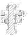
図1は、本発明の第1実施形態の振動波モータ1を説明する図である。
本実施形態では振動子10側を固定とし、移動子(相対運動部材)20を駆動する様になっている。
移動子20は、アルミニウム等の軽金属からなり、摺動面の表面には耐摩耗性向上のための表面処理が成されている。
(First embodiment)
Hereinafter, embodiments of a vibration wave motor 1 according to the present invention will be described in detail with reference to the accompanying drawings.
FIG. 1 is a diagram illustrating a vibration wave motor 1 according to a first embodiment of the present invention.
In this embodiment, the
The
振動子10は、後で説明する様に電気エネルギ−を機械エネルギ−に変換する圧電素子や電歪素子等を例とした電気機械変換素子(以下、圧電体と称する)11と、圧電体11が接合された弾性体12と、から構成され、振動子10には進行性振動波が発生する。
As will be described later, the
弾性体12は、共振先鋭度が大きな金属材料から成り、形状は円環形状である。
弾性体12の一面(接合面12f)には圧電体11が接合され、その一面と反対側は溝12bが切られている。そして、突起部分(溝12bがない箇所)12cの先端は駆動面12aとなって移動子20に加圧接触される。
弾性体12の溝12bが切られていない部分はベース部12dであり、ベース部12dから内径側にフランジ12eが伸延されている。フランジ12eの最内径部は、固定部材13に固定されている。
弾性体12の突起部分12cには、全体を覆う様にして塗装膜や潤滑メッキ等の摺動部材が施されている。
The
The
The portion of the
The protruding
圧電体11は、後に詳述するが、弾性体12の接着面と反対側の面(FPC側の面、反接合面、以後、この面を表面という)には、電極が配置され、それは円周方向に沿って2つの相(A相、B相)に分かれた2群構造となっている。
各相においては、1/2波長毎に交互に分極され、A相とB相との間には1/4波長分間隔があくように電極が配置されている。
As will be described in detail later, the
In each phase, electrodes are arranged so that they are alternately polarized every ½ wavelength, and an interval of ¼ wavelength is provided between the A phase and the B phase.
出力軸21は、ゴム部材22と出力軸21のDカットにはまるように挿入されたストッパー部材23を介して移動子20に結合されている。そして、出力軸21とストッパー部材23はEクリップ24等により固定され、移動子20と一体に回転する様にされている。
ストッパー部材23と移動子20との間のゴム部材22は、ゴムによる粘着性で移動子20とストッパー部材23と結合する機能があり、かつ移動子20からの振動を出力軸21へ伝えないための振動吸収との機能があるブチルゴム等が好適である。
加圧部材25は、出力軸21の出力ギア41とベアリング27との間に設けられている。この様な構造により、移動子20は弾性体12の駆動面12aに加圧接触する。
The
The
The
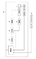
図2は、第1実施形態の振動波モータ1の駆動装置30を説明するブロック図である。
まず、振動波モータ1の駆動/制御部31について説明する。
発振部32は、制御部31の指令により所望の周波数の駆動信号を発生する。
移相部33は、発振部32で発生した駆動信号を位相の異なる2つの駆動信号に分ける。
FIG. 2 is a block diagram illustrating the
First, the drive /
The oscillating
The
増幅部34は、移相部33によって分けられた2つの駆動信号をそれぞれ所望の電圧に昇圧する。
増幅部34からの駆動信号は、振動波モータ1に伝達され、この駆動信号の印加により振動子10に進行波が発生し、移動子20が駆動される。
回転検出部35は、光学式エンコーダや磁気エンコーダ等により構成され、移動子20の駆動によって駆動された駆動物の位置や速度を検出し、検出値を電気信号として制御部31に伝達する。
The amplifying
A drive signal from the amplifying
The
制御部31は、レンズ鏡筒110内またはカメラ本体のCPU36からの駆動指令を基に振動波モータ1の駆動を制御する。制御部31は、回転検出部35からの検出信号を受け、その値を基に、位置情報と速度情報を得て、目標位置に位置決めされるように発振部32の周波数を制御する。
The
次に、第1実施形態の振動波モータ1の動作を説明する。
制御部31から駆動指令が発令されると、発振部32は駆動信号を発生させる。
その駆動信号は移相部33により90度位相の異なる2つの駆動信号に分割され、増幅部34により所望の電圧に増幅される。
増幅された駆動信号は、振動波モータ1の圧電体11に印加され、圧電体11は励振(振動)される。その圧電体11の励振によって、弾性体12には4次の曲げ振動が発生する。圧電体11はA相とB相とに分けられており、駆動信号はそれぞれA相とB相に印加される。
Next, the operation of the vibration wave motor 1 of the first embodiment will be described.
When a drive command is issued from the
The drive signal is divided into two drive signals having a phase difference of 90 degrees by the
The amplified drive signal is applied to the
A相から発生する4次曲げ振動とB相から発生する4次曲げ振動とは位置的な位相が1/4波長ずれるようになっている。また、A相駆動信号とB相駆動信号とは90度位相がずれているため、2つの曲げ振動は合成され、4波の進行波となる。 The positional phase of the quaternary bending vibration generated from the A phase and the quaternary bending vibration generated from the B phase are shifted by ¼ wavelength. In addition, since the phase A drive signal and the phase B drive signal are 90 degrees out of phase, the two bending vibrations are combined into four traveling waves.
進行波の波頭には楕円運動が生じる。従って、駆動面12aに加圧接触された移動子20は、この楕円運動によって摩擦的に駆動される。
移動子20の駆動により駆動された駆動体には、光学式エンコ−ダが配置されていて、そこから、電気パルスが発生し、制御部31に伝達される。制御部31は、この信号を基に、現在の位置と現在の速度を得ることが可能となる。
Elliptic motion occurs at the front of the traveling wave. Therefore, the
An optical encoder is arranged in the driving body driven by driving the moving
図3は、第1実施形態の振動波モータ1を搭載したレンズ鏡筒110を示す図である。
振動波モータ1はギアユニットモジュール113に取り付けられ、ギアユニットモジュール113はレンズ鏡筒110鏡筒の固定筒114に取り付けられている。
振動波モータ1の出力ギア41は、ギアユニットモジュール113の減速ギア115を介して、カム環116に回転運動が伝達され、カム環116は回転駆動する。
カム環116には、周方向に対して斜めにキー溝117が切られており、該キー溝117に固定ピン118が挿入されたAF環119は、カム環116が回転駆動することにより、光軸OA方向に直進方向に駆動され、所望の位置に停止できる様にされている。
回路121は、レンズ鏡筒110の外側固定筒114aと内側固定筒114bとの間に設けられ、振動波モータ1の駆動、制御、回転数の検出、振動センサーの検出等を行う。
FIG. 3 is a diagram illustrating the
The vibration wave motor 1 is attached to the
The rotational motion of the
A
The
次に、圧電体11について詳述する。
図4は、第1実施形態の圧電体11を説明する図である。図4(a)は圧電体11の側面図(振動波モータ1の加圧方向と直交する方向から見た図)の一部である。図4(b)は圧電体11の表面11Aを示した図であり、(a)は(b)のa−a方向から見た図である。図4(c)は(b)のc−c断面図である。図4(d)は圧電体11の裏面11Bを示した図である。
図5は、圧電体11と弾性体12とを含む振動子10を説明する図である。図5(a)は側面図であり、図5(b)は表面側から見た図である。
Next, the
FIG. 4 is a diagram illustrating the
FIG. 5 is a diagram illustrating the
圧電体11の素地は、PZTと呼ばれるチタン酸ジルコン酸鉛、または、近年では環境問題から鉛フリーの材料であるチタン酸バリウム、チタン酸ビスマスナトリウム、チタン酸ビスマスカリウム等から構成されている。
圧電体11の素地の表面11Aには、電極が配置され、銀ペーストが印刷されている。電極はNiPや金等の金属メッキでも良い。
The substrate of the
Electrodes are arranged on the
また、圧電体11は、図4(a),(c),図5に示すように、単層圧電体111(第1層圧電体111a、第2層圧電体111b及び第3層圧電体111c)を複数層(本実施形態では3層)積層したものである。以下、圧電体11を、単層圧電体111と区別するために、適宜、積層圧電体11という。
第1層圧電体111a、第2層圧電体111b及び第3層圧電体111cは、この順で、積層圧電体11の表面11A側から並んでいる。
Further, as shown in FIGS. 4A, 4C, and 5, the
The first-
図6は、単層圧電体111それぞれの電極パターンを説明する図である。図6(a)は単層圧電体111それぞれの表裏面の電極パターンを示した図であり、図6(b)は積層圧電体11における単層圧電体111それぞれの分極方向を示した図である。
FIG. 6 is a diagram for explaining the electrode patterns of each single-layer piezoelectric body 111. 6A is a diagram showing the electrode patterns on the front and back surfaces of each single-layer piezoelectric body 111, and FIG. 6B is a diagram showing the polarization directions of each single-layer piezoelectric body 111 in the laminated
図6に示すように、第1層圧電体111aの表面111aA、第2層圧電体111aの裏面111bB、第3層圧電体111cの表面111cAには、印加電極パターン16が形成され、それは円周方向に沿って2つの相(A相、B相)に分かれている。
各相においては、1/2波長毎に交互に分極され、A相とB相との間には1/4波長分間隔があくように、電極パターン17が配置されている。
As shown in FIG. 6, the applied
In each phase,
第1層圧電体111aの裏面111aB、第2層圧電体111bの表面111bA、第3層圧電体111cの裏面111cBには、分割した電極パターン16ではなく、2つの駆動信号の相(A相、B相)の共通電極とする共通電極パターン19が形成されている。
The back surface 111aB of the first
そして、第1層圧電体111aの裏面111aBと第2層圧電体111bの表面111bAとは貼り合わされ、第2層圧電体111bの裏面111bBと第3層圧電体111cの表面111cAとは貼り合わされ、積層圧電体11が形成されている。
The back surface 111aB of the first
第1層圧電体111aの表面111aAは、積層圧電体11全体としての表面11Aとなり、第3層圧電体111cの裏面111cBは、積層圧電体11全体としての裏面11Bとなる。
積層圧電体11としての表面11Aには、図5(a),(b)に示すように駆動信号を伝達するためにフレキシブルプリント基板(FPC)14が接着剤18で接着されている。接着剤18は、弾性体12及び圧電体11の側面からFPC14まで延びるように塗布されて、接着強度が補強されている。
また、積層圧電体11としての裏面11Bは、常温硬化性の接着剤により弾性体12に接合されている。
The surface 111aA of the first
As shown in FIGS. 5A and 5B, a flexible printed circuit board (FPC) 14 is adhered to the
Further, the
図6(b)に示すように、各層(第1層圧電体111a,第2層圧電体111b,第3層圧電体111c)の分極は、奇数層の接合面(弾性体側の面、以後、こちら側を裏面という)側から表面側への分極方向と、偶数層の裏面側から表面側へ分極方向が反対となっている。
As shown in FIG. 6B, the polarization of each layer (the first
すなわち、図6(b)に示す領域Pにおける第1層圧電体111aにおいて、裏面111aB側から表面111aA側へ向かう分極方向だった場合(この方向を+方向とする)、第2層圧電体111bでは、表面111bAから裏面111bBへ向かう分極方向(−方向)となり、さらに第3層圧電体111cでは、裏面111cBから表面111cAへ向かう分極方向(+方向)となる。すなわち、分極方向が圧電体の厚さ方向に沿って+−+となる。
また、領域Pと隣接する領域Qでは、領域Pと分極方向が逆で、圧電体の厚さ方向に沿って−+−となる。
That is, in the first
Further, in the region Q adjacent to the region P, the polarization direction is opposite to that of the region P, and becomes − + − along the thickness direction of the piezoelectric body.
また、上記の様な電極および分極の構成において、圧電体11における単層圧電体111の積層数は奇数となる。すなわち、第1層の分極方向と最終層の分極方向とが同じになるので、単層圧電体111の数は奇数となる。
In the electrode and polarization configuration as described above, the number of single-layer piezoelectric bodies 111 in the
奇数層の裏面側の電極パターンと偶数層の表側の電極パターンとは、同じ電極パターンとなり、偶数層の裏面側の電極パターンと奇数層の表面側の電極パターンとは、同じ電極パターンとなる。 The electrode pattern on the back side of the odd layer and the electrode pattern on the front side of the even layer are the same electrode pattern, and the electrode pattern on the back side of the even layer and the electrode pattern on the front side of the odd layer are the same electrode pattern.
すなわち、奇数層(本実施形態では第1層圧電体111aと第3層圧電体111c)の裏面111aB,111cBと偶数層(本実施形態では第2層圧電体111b)の表面111bAの電極パターンは同じとなる。
本実施形態においてはこれらの面には、円周方向に沿って2つの駆動信号の相(A相、B相)に分かれ、各相においては、1/2波長毎に交互に図の様に分極され、A相とB相との間には1/4波長分間隔が空く様に印加電極パターン16が配置されている。
That is, the electrode patterns on the back surfaces 111aB and 111cB of the odd-numbered layers (the first-
In this embodiment, these surfaces are divided into two drive signal phases (A phase and B phase) along the circumferential direction, and in each phase, every half wavelength alternately as shown in the figure. The
また、奇数層(本実施形態では第1層圧電体111aと第3層圧電体111c)の表面111aA,111cAと偶数層(本実施形態では第2層圧電体111b)の裏面111bBの電極パターンは同じとなる。本実施形態においては、分割した印加電極パターン16ではなく、2つの駆動信号の相(A相、B相)の共通電極パターン19が形成されている。
Further, the electrode patterns of the front surfaces 111aA and 111cA of the odd-numbered layers (first
なお、本実施形態では、説明を簡単にするため、3層を例としたが、5層、7層、9層・・・と、奇数の積層数なら同様の構成とすることができる。
また、進行波の波数を4波として説明したが、5波、6波、7波・・・と、どの様な波数でも良い。
In this embodiment, for simplicity of explanation, three layers are used as an example. However, if the number of layers is five, seven, nine,.
Further, although the wave number of the traveling wave has been described as four waves, any wave number such as five waves, six waves, seven waves, etc. may be used.
ここで、図4(a),(c),図5に示すように、単層圧電体111(第1層圧電体111a,第2層圧電体111b及び第3層圧電体111c)は、それぞれ円環形状を有している。その外径は、それぞれ異なり、第1層圧電体111a,第2層圧電体111b及び第3層圧電体111cの順に外径が小さくなっている。
すなわち、図4(c)に示すように、第1層圧電体111aの外径ra,第2層圧電体111bの外径rb及び第3層圧電体111cの外径rcとすると、ra<rb<rcとなっている。なお、本実施形態で内径は同一である。
Here, as shown in FIGS. 4A, 4C, and 5, the single-layer piezoelectric body 111 (the first-
That is, as shown in FIG. 4C, when the outer diameter ra of the first
このため、図4(c)、図5に示すように、積層圧電体11としてみたときに、断面図における外径側は段階状になっている。図7は、積層圧電体11の段階状部分の拡大図である。図7(a)は、後述の共通導通部18aが設けられている部分、図7(b)は後述の印加導通部18bが設けられている部分である。
そして、第1層圧電体111aの表面11A側から見たときに、第2層圧電体111bの表面11Aの外周側は、第1層圧電体111aと重ならずに露出した露出部40bとなっている。さらに第3層圧電体111cの外周側は、第2層圧電体111bと重ならずに露出した露出部40cとなっている。
Therefore, as shown in FIGS. 4C and 5, when viewed as the laminated
When viewed from the
また、図4(b),(c),図7に示すように、それぞれの電極パターン16,17,19は、円環の外縁と内縁とから離間して形成されている。そして、この円環の外縁と電極パターン16,17,19との間の離間している部分の一部が、上述の露出部40b,40cとなる。
Further, as shown in FIGS. 4B, 4C, and 7, the
本実施形態において、この離間部分(露出部40b,40c)には、それぞれの電極パターン16,17,19から外縁まで延びる延伸部16a,17a,19aが形成されている。
In the present embodiment, extending
そして、図7(a)に示すように、第1層圧電体111aの表面111aAの電極パターン17と、第1層圧電体111aの延伸部17aと、第1層圧電体111aの側面111asと、第2層圧電体111bの表面111bAの延伸部19a(露出部40b)と、第2層圧電体111bの側面111bsと、第3層圧電体111cの表面111cAの延伸部17a(露出部40c)と、第3層圧電体111cの側面111csと、共通電極パターン19とを接続するように共通導通部18aが延びている。なお共通導通部18aは、例えば導電性塗料を塗布することで形成される。
7A, the
ここで、第2層圧電体111bの表面111bAの延伸部19aは、第2層圧電体111bの表面111bAの共通電極パターン19と、第1層圧電体111aの裏面111bBの共通電極パターン19に接続される。
また、第3層圧電体111cの表面111cAの延伸部17aは、第3層圧電体111cの電極パターン17、第2層圧電体111bの電極パターン17とに接続される。
Here, the extending
The extending
すなわち、第1層圧電体111aの表面111aAの電極パターン17と、第1層圧電体111aの裏面111aBの共通電極パターン19と、第2層圧電体111bの表面111bAの共通電極パターン19と、第2層圧電体111bの裏面111bBの電極パターン17と、第3層圧電体111cの表面111cAの電極パターン17と、第3層圧電体111cの裏面111cBの共通電極パターン19と、が共通導通部18aによって接続される。
That is, the
また図7(b)に示すように、第1層圧電体111aの表面111aAの印加電極パターン16と、第1層圧電体111aの延伸部16aと、第1層圧電体111aの側面111asと、第2層圧電体111bの表面111bAの露出部40bと、第2層圧電体111bの側面111bsと、第3層圧電体111cの表面111cAの延伸部16aと印加電極パターン16とを接続するように印加導通部18bが延びている。
7B, the applied
ここで、第2層圧電体111bの表面111bAの露出部40bに設けられた印加導通部18bは、第2層圧電体111bの表面111bAの共通電極パターン19と第1層圧電体111aの裏面111bBの共通電極パターン19とに接続されていない。
一方、第3層圧電体111cの表面111cAの延伸部16aは、第3層圧電体111cの印加電極パターン16、第2層圧電体111bの印加電極パターン16に接続される。
Here, the applied conducting
On the other hand, the extending
すなわち、第1層圧電体111aの表面111aAの印加電極パターン16と、第2層圧電体111bの裏面111bBの印加電極パターン16と、第3層圧電体111cの表面111cAの印加電極パターン16と、が印加導通部18bによって接続される。
That is, the applied
なお、本実施形態では、各層の電極パターン16,19の導通を外周側面側にて実施しているが、段階形状を内周側に形成して、導通を内周面側で導通させても良い。
In this embodiment, the
図8は印加電圧による圧電体11の伸縮を示した図である。駆動信号が+に印加された場合、A相およびB相の各電極は、図8(a)の様に伸延および縮小が交互になされる。すなわち、領域Pにおいては伸延し、領域Qは縮小する。
また、逆に駆動信号が−に印加された場合、上記と逆に、図8(b)のように各電極は伸延および縮小が交互になされる。すなわち、領域Pにおいては縮小し、領域Qは伸延する。
このように、本実施形態の構成では、印加電圧と伸縮方向においては従来の単層の圧電体11と同じ挙動を示す。
FIG. 8 shows the expansion and contraction of the
On the other hand, when the drive signal is applied to-, contrary to the above, each electrode is alternately extended and reduced as shown in FIG. 8B. That is, the area P is reduced and the area Q is distracted.
Thus, in the configuration of the present embodiment, the same behavior as that of the conventional single-
このように、本実施形態によると、積層圧電体11を構成する単層圧電体111が段階状に積層されている。そして、段階部分は表面が露出しており、その露出部40b,40cには、それぞれの単層圧電体111の表裏に形成された電極パターンから導通して延びる延伸部16a,17a,19aが設けられている。
この延伸部16a,17a,19aの露出している部分に導電性塗料を塗布することで、積層圧電体間の導通を、容易且つ確実に図ることができる。
As described above, according to the present embodiment, the single-layer piezoelectric bodies 111 constituting the multilayered
By applying a conductive paint to the exposed portions of the extending
また、圧電体における伸縮(変形)の大きさは、圧電体内部に生じる電界の強度によって異なる。すなわち、印加電圧が同じならば、圧電体が薄いほうが電界が強くなる。
したがって、圧電体は薄いほうがよいが、単層の圧電体を薄くすると強度的に不十分である。しかし、本実施形態によると、単層圧電体の厚さを薄くしても積層することで強度が確保できる。
Further, the magnitude of expansion / contraction (deformation) in the piezoelectric body varies depending on the strength of the electric field generated inside the piezoelectric body. That is, if the applied voltage is the same, the thinner the piezoelectric body, the stronger the electric field.
Therefore, it is better that the piezoelectric body is thin. However, if the single-layer piezoelectric body is thin, the strength is insufficient. However, according to the present embodiment, the strength can be ensured by stacking even if the thickness of the single-layer piezoelectric body is reduced.
そして、単層圧電体それぞれを薄くすることが可能となるため、印加電圧をそれほど高くしなくとも、大きな変形量を得ることができる。すなわち、昇圧回路等を用いずに実用的な変形量を確保することができる。 Since each single-layer piezoelectric body can be made thin, a large amount of deformation can be obtained without increasing the applied voltage so much. That is, a practical amount of deformation can be ensured without using a booster circuit or the like.
さらに、積層の際、同一の電極パターンを有する単層圧電体111を、向きを変えて交互に配置している。すなわち、異なる電極パターンの単層圧電体を用いることなく、同一の電極パターンを有する単層圧電体111によって積層圧電体11を形成している。このため、コストダウンが可能となり、製造工程が単純化され、作業上のミスが低減され、歩留まりや圧電特性の品質を向上することが可能となる。
Furthermore, the single-layer piezoelectric bodies 111 having the same electrode pattern are alternately arranged in different directions during lamination. That is, the laminated
本実施形態によると、単層圧電体111を積層し、導通部18aによって各層を導通させているので、単層圧電体111全てを、一つの印加電圧で同時に分極することが可能である。
According to this embodiment, since the single-layer piezoelectric body 111 is laminated and each layer is made conductive by the conducting
このように本実施形態によると、振動波モータ1として組立てた場合に、従来よりも駆動電圧を下げることができ、駆動効率や発生トルク等の振動波モータ1の性能を向上すること可能となる。 As described above, according to the present embodiment, when the vibration wave motor 1 is assembled, the drive voltage can be lowered as compared with the conventional case, and the performance of the vibration wave motor 1 such as drive efficiency and generated torque can be improved. .
本実施形態は、駆動電圧が大きくなる、小径タイプの進行波型振動波モータ1に対して、その駆動性能向上への効果が大きい。特に、外径が25mm以下の場合に、本実施形態の効果が顕著である。 This embodiment has a great effect on driving performance of the small-diameter type traveling wave type vibration wave motor 1 in which the driving voltage increases. In particular, when the outer diameter is 25 mm or less, the effect of this embodiment is remarkable.
また、小径タイプの進行波型振動波モータ1は、波長を得るために、4波、5波と波数を少なくする必要があるが、波数を少なくすると、A相およびB相の電極パターン数が少なくなる。
本実施形態の4波の場合、A相(またはB相)の電極パターン数は4、5波の場合では、A相(またはB相)の電極パターン数は5となるが、各相の電極パターン数が少ないと、屈曲振動の励起がされにくい。
Further, in order to obtain a wavelength, the small-diameter type traveling wave type vibration wave motor 1 needs to reduce the number of waves to 4 waves and 5 waves, but if the number of waves is reduced, the number of electrode patterns of the A phase and the B phase is reduced. Less.
In the case of four waves in the present embodiment, the number of electrode patterns of A phase (or B phase) is 4, and in the case of five waves, the number of electrode patterns of A phase (or B phase) is 5, but the electrodes of each phase When the number of patterns is small, bending vibration is difficult to be excited.
従って、本実施形態のように、各圧電体層とも分極され、圧電特性が得られる様になっている必要がある。本発明では、進行波の波数が4波、5波の場合に特に効果が得られる。 Therefore, as in the present embodiment, each piezoelectric layer needs to be polarized so that piezoelectric characteristics can be obtained. In the present invention, the effect is particularly obtained when the number of traveling waves is four or five.
(第2実施形態)
図9は、本発明の第2実施形態の圧電体11’を説明する図であり、第1実施形態の図4に対応している。第1実施形態と同様の部分には同一の符号を付し、その説明を省略する。
図9(a)は第2実施形態の圧電体11’の側面図の一部である。図9(b)は圧電体11’の表面11Aを示した図であり、(a)は(b)のa−a方向から見た図である。図9(c)は(b)のc−c断面図である。図9(d)は圧電体11’の裏面11Bを示した図である。さらに図9(e)は(b)の点線の丸で囲った部分の拡大図である。
(Second Embodiment)
FIG. 9 is a diagram illustrating a
FIG. 9A is a part of a side view of the
第1実施形態では、外径の異なる単層圧電体111を積層することで、外周側を段階状として露出部40b,40cを形成した。第2実施形態では圧電体11’に切欠き50を設け、この切欠き50を周方向にずらすことによって段階部分を形成して露出部40b,40cを設ける。
すなわち、単層圧電体111の電極パターンの外周部に半円状の第1切欠き部50を設け、そこへ各電極パターン16,17,19から延伸部16a,17a,19aを延ばす。
In the first embodiment, the exposed
That is, the semicircular
単層圧電体111を積層させる際に、第1切欠き部50が各層で周方向側に少しずつずれるようにする。この際、第1層圧電体111aの第1切欠き部50から、第2層圧電体111b及び第3層圧電体111cの延伸部16a,17a,19aが見えるようにする。すなわち、第1層圧電体111aの第1切欠き部50の内部に、第2層圧電体111b及び第3層圧電体111cの延伸部16a,17a,19aが露出しているようにずらす。
When laminating the single-layer piezoelectric body 111, the
また、このようにずらすために、本実施形態では、各層に基準となる切欠き部(第2切欠き部51)を設ける。第2切欠き部51と第1切欠き部との距離は各層で異なる。
第1層圧電体111aにおける第2切欠き部51と第1切欠き部50との間の距離よりも、第2層圧電体111bにおける第2切欠き部51と第1切欠き部50との間の距離が大きく、さらにそれよりも第3層圧電体111cにおける第2切欠き部51と第1切欠き部50との間の距離が大きい。
In order to shift in this way, in this embodiment, a reference cutout (second cutout 51) is provided in each layer. The distance between the
The distance between the
単層圧電体111を積層する際に、この第2切欠き部51の位置を、厚さ方向において全ての層で一致させると、第1層圧電体111aの第1切欠き部50から、第2層圧電体111b及び第3層圧電体111cの表面に設けられた延伸部16a,17a,19aが見えるようにずれ、段階部が形成される。
本実施形態によっても、第1切欠き部50の段階部に導電塗料を塗布することで、第1実施形態と同様に、単層圧電体111の電極間を導通させることができる。
When the single-layer piezoelectric body 111 is laminated, if the positions of the
Also in the present embodiment, by applying a conductive paint to the stepped portion of the
(第3実施形態)
図10は、本発明の第3実施形態のレンズ鏡筒200を説明する図である。本発明は第1実施形態の小径タイプの振動波モータ1の圧電体11のみならず、大径円環タイプの振動波モータ210の圧電体11においても同様な構成にすることが可能で、第1実施形態と同じ効果が得られる。
(Third embodiment)
FIG. 10 is a diagram illustrating a
まず、振動波モータ210の構成を説明する。
振動子211は、圧電体11と、圧電体11を接合した弾性体214とから構成されている。振動子211には進行波が発生するようにされているが、本実施形態では一例として9波の進行波として説明する。
弾性体214は、共振先鋭度が大きな金属材料から成り、円環形状となっている。圧電体11が接合される反対面には溝が切ってあり、溝が設けられていない部分の面が駆動面216aとなり移動子220に加圧接触される。弾性体214の駆動面216aの表面には、駆動性能確保および耐久性向上のために潤滑塗装膜が施されている。
First, the configuration of the
The
The
圧電体11は、円周方向に沿って2つの相(A相、B相)に分かれており、各相においては、1/2波長毎に分極が交互となった要素が並べられていて、A相とB相との間には1/4波長分間隔が空くようにしてある。
The
圧電体11の下には、不織布252、加圧部材250が配置されている。
不織布252は、フェルトを例としたものであり、圧電体11の下に配置され、振動子211の振動を加圧部材250に伝えないようにしてある。
A
The
加圧部材250は、加圧板(図示せず)の下に配置されていて、加圧力を発生させるものである。本実施形態では、加圧部材250を皿バネとする、皿バネでなくともコイルバネやウェーブバネでも良い。加圧部材250は、押さえ環251は固定部材223に固定されることで、保持される。
The
移動子220は、アルミニウムといった軽金属からなり、摺動面の表面には耐摩耗性向上のための摺動材料が設けられている。
移動子220の上には、移動子220の縦方向の振動を吸収するために、ゴムの様な振動吸収部材243が配置され、その上には出力伝達部材242が配置されている。
The
On the moving
出力伝達部材242は、固定部材223に設けられたベアリング253により、加圧方向と径方向とを規制し、これにより移動子220の加圧方向と径方向とが規制されるようにされている。
出力伝達部材242は、突起部241があり、そこからカム環315に接続されたフォークがかん合しており、出力伝達部材242の回転とともに、カム環315が回転される。
The
The
カム環315には、キー溝317がカム環315に斜めに切られており、AF環319に設けられた固定ピン318が、キー溝317にかん合していて、カム環315が回転駆動することにより、光軸方向に直進方向にAF環319が駆動され、所望の位置に停止できる様にされている。
固定部材223は、押さえ環251がネジにより取り付けられ、これを取り付けることで、出力伝達部材242から移動子220、振動子211、加圧部材250までを一つのモータユニットとして構成できるようになる。
In the
In the fixing
第3実施形態の圧電体213も、第1実施形態の圧電体11と同様の積層圧電体である。
すなわち、単層圧電体を複数層(本実施形態では3層)積層したものである。第1層圧電体、第2層圧電体及び第3層圧電体が、この順で、積層圧電体の弾性体との接着面と反対側から並んでいる。
The
That is, a single-layer piezoelectric body is laminated by a plurality of layers (three layers in this embodiment). The first-layer piezoelectric body, the second-layer piezoelectric body, and the third-layer piezoelectric body are arranged in this order from the side opposite to the adhesive surface of the laminated piezoelectric body with the elastic body.
そして、第1層圧電体の表面側には、電極が配置され、それは、円周方向に沿って2つの駆動信号の相(A相、B相)に分かれている。各相においては、1/2波長毎に交互に分極され、A相とB相との間には1/4波長分間隔が空く様に電極が配置されている。
第1層圧電体の裏面は、分割した電極パターンではなく、2つの駆動信号の相(A相、B相)の共通電極パターンが形成されている。
And the electrode is arrange | positioned at the surface side of the 1st layer piezoelectric material, and it is divided into the phase (A phase, B phase) of two drive signals along the circumferential direction. In each phase, the electrodes are arranged so that they are alternately polarized every ½ wavelength, and an interval of ¼ wavelength is left between the A phase and the B phase.
On the back surface of the first layer piezoelectric body, not a divided electrode pattern but a common electrode pattern of two drive signal phases (A phase and B phase) is formed.
第2層圧電体の表面は、分割した電極パターンではなく、2つの駆動信号の相(A相、B相)の共通電極パターンが形成されている。そして、第2層目の表面と第1層目の裏面Bとは貼り合わされている。
第2層圧電体の裏面側には、電極が配置され、それは円周方向に沿って2つの駆動信号の相(A相、B相)に分かれている。各相においては、1/2波長毎に交互に分極され、A相とB相との間には1/4波長分間隔が空く様に電極16が配置されている。
On the surface of the second layer piezoelectric body, not a divided electrode pattern but a common electrode pattern of two drive signal phases (A phase and B phase) is formed. The surface of the second layer and the back surface B of the first layer are bonded together.
An electrode is disposed on the back surface side of the second layer piezoelectric body, which is divided into two drive signal phases (A phase and B phase) along the circumferential direction. In each phase, the
第3層圧電体の表面は、電極が配置され、それは円周方向に沿って2つの駆動信号の相(A相、B相)に分かれている。各相においては、1/2波長毎に交互に分極され、A相とB相との間には1/4波長分間隔が空く様に電極が配置されている。そして、第2層圧電体の裏面と第3層圧電体の表面とは貼り合わされている。
第3層圧電体の裏面は、分割した電極パターンではなく、2つの駆動信号の相(A相、B相)の共通電極パターンが形成されている。
そして、第3実施形態においても、積層圧電体を構成する単層圧電体は段階状に積層されている。そして、段階部分は表面が露出しており、その露出部に導通部が設けられてい。
以上、第3実施形態においても、上記第1実施形態と同様の効果を有する。
Electrodes are arranged on the surface of the third layer piezoelectric body, which is divided into two drive signal phases (A phase and B phase) along the circumferential direction. In each phase, the electrodes are arranged so that they are alternately polarized every ½ wavelength, and an interval of ¼ wavelength is left between the A phase and the B phase. The back surface of the second layer piezoelectric body and the front surface of the third layer piezoelectric body are bonded together.
On the back surface of the third layer piezoelectric body, not a divided electrode pattern, but a common electrode pattern of two drive signal phases (A phase and B phase) is formed.
Also in the third embodiment, the single-layer piezoelectric bodies constituting the multilayered piezoelectric body are laminated stepwise. And the surface of the step portion is exposed, and a conductive portion is provided in the exposed portion.
As described above, the third embodiment has the same effect as that of the first embodiment.
1:振動波モータ、10:振動子、11:圧電体(積層圧電体)、12:弾性体、12a:駆動面、12f:接合面、16:印加電極パターン、16a:延伸部、17:電極パターン、17a:延伸部、18a:共通導通部、18b:印加導通部、19:共通電極パターン、20:移動子、50:第1切欠き部、51:第2切欠き部、110:レンズ鏡筒、111:単層圧電体、111a:第1層圧電体、111b:第2層圧電体、111c:第3層圧電体、200:レンズ鏡筒、210:振動波モータ、211:振動子、213:圧電体、214:弾性体、218a:駆動面、220:移動子 1: vibration wave motor, 10: vibrator, 11: piezoelectric body (laminated piezoelectric body), 12: elastic body, 12a: driving surface, 12f: bonding surface, 16: applied electrode pattern, 16a: extending portion, 17: electrode Pattern, 17a: Extension part, 18a: Common conduction part, 18b: Applied conduction part, 19: Common electrode pattern, 20: Mover, 50: First notch part, 51: Second notch part, 110: Lens mirror 111, single layer piezoelectric body, 111a: first layer piezoelectric body, 111b: second layer piezoelectric body, 111c: third layer piezoelectric body, 200: lens barrel, 210: vibration wave motor, 211: vibrator, 213: Piezoelectric body, 214: Elastic body, 218a: Driving surface, 220: Mover
Claims (6)
前記積層体に接合される接合面、及び該接合面の反対側に設けられ、前記振動によって進行性の振動波を生じる駆動面、を有する弾性体と、
前記駆動面に加圧接触され、前記振動波によって駆動される相対運動部材と、を備え、
前記積層体は、前記電気機械変換素子の単層体が、前記弾性体の厚さ方向へ、複数積層されたものであり、
前記積層体を前記接合面と平行な一方の面側からみたときに、後方の単層体において前方の単層体と重ならずに表面が露出している露出部が存在し、該露出部は段階状に連続し、
その連続する露出部に前記単層体間の導通部が形成されていること、
を特徴とする振動波モータ。 A laminate of electromechanical transducers in which vibration is generated by a drive signal;
An elastic body having a bonding surface to be bonded to the laminate and a driving surface that is provided on the opposite side of the bonding surface and generates a progressive vibration wave by the vibration;
A relative motion member that is in pressure contact with the drive surface and driven by the vibration wave,
In the laminate, a plurality of monolayers of the electromechanical conversion element are laminated in the thickness direction of the elastic body,
When the laminate is viewed from one side parallel to the joint surface, there is an exposed portion where the surface is exposed without overlapping the front monolayer in the rear monolayer, and the exposed portion Is continuous in stages,
That a continuous portion between the monolayers is formed in the continuous exposed portion;
Vibration wave motor characterized by
前記単層体は円環形状であり、前記露出部は、円環の外周側または内周側に形成されていること、
を特徴とする振動波モータ。 The vibration wave motor according to claim 1,
The monolayer has an annular shape, and the exposed portion is formed on an outer peripheral side or an inner peripheral side of the annular shape;
Vibration wave motor characterized by
前記単層体は外周側または内周側の径が互いに異なり、該径の異なる前記単層体を積層させることにより、前記露出部が段階状に形成されていること、
を特徴とする振動波モータ。 In the vibration wave motor according to claim 1 or 2,
The single-layer body has different outer diameters or inner-periphery diameters, and the exposed portions are formed stepwise by laminating the single-layer bodies having different diameters.
Vibration wave motor characterized by
前記単層体には、それぞれ第1切欠き部が設けられており、前記単層体を積層させる際に、該第1切欠き部の位置が互いにずれることにより、前記露出部が段階状に形成されていること、
を特徴とする振動波モータ。 In the vibration wave motor according to claim 1 or 2,
Each of the single-layer bodies is provided with a first notch, and when the single-layer bodies are stacked, the positions of the first notches are shifted from each other, so that the exposed portion is stepped. Being formed,
Vibration wave motor characterized by
前記単層体には、前記第1切欠き部とは異なる第2切欠き部が設けられており、
前記第1切欠き部と前記第2切欠き部との間の距離は、前記単層体によって異なり、
前記単層体を積層させる際に、前記第2切欠き部が前記厚さ方向に整列するように前記単層体を並べることにより、前記第1切欠きの縁部において前記露出部が段階状に形成されること、
を特徴とする振動波モータ。 The vibration wave motor according to claim 4,
The single layer body is provided with a second cutout portion different from the first cutout portion,
The distance between the first notch and the second notch varies depending on the monolayer,
When laminating the single-layer body, the exposed portions are stepped at the edge of the first notch by arranging the single-layer bodies so that the second notch portions are aligned in the thickness direction. Formed into,
Vibration wave motor characterized by
Priority Applications (2)
| Application Number | Priority Date | Filing Date | Title |
|---|---|---|---|
| JP2012151991A JP2014017909A (en) | 2012-07-06 | 2012-07-06 | Vibration wave motor and lens barrel |
| PCT/JP2013/068556 WO2014007383A1 (en) | 2012-07-06 | 2013-07-05 | Vibration wave motor and lens barrel |
Applications Claiming Priority (1)
| Application Number | Priority Date | Filing Date | Title |
|---|---|---|---|
| JP2012151991A JP2014017909A (en) | 2012-07-06 | 2012-07-06 | Vibration wave motor and lens barrel |
Publications (1)
| Publication Number | Publication Date |
|---|---|
| JP2014017909A true JP2014017909A (en) | 2014-01-30 |
Family
ID=50112131
Family Applications (1)
| Application Number | Title | Priority Date | Filing Date |
|---|---|---|---|
| JP2012151991A Pending JP2014017909A (en) | 2012-07-06 | 2012-07-06 | Vibration wave motor and lens barrel |
Country Status (1)
| Country | Link |
|---|---|
| JP (1) | JP2014017909A (en) |
Cited By (2)
| Publication number | Priority date | Publication date | Assignee | Title |
|---|---|---|---|---|
| JP2016226175A (en) * | 2015-05-29 | 2016-12-28 | キヤノン株式会社 | Piezoelectric body, vibrator and vibration wave motor |
| JP2020043095A (en) * | 2018-09-06 | 2020-03-19 | Njコンポーネント株式会社 | Laminated type piezoelectric element and manufacturing method therefor |
-
2012
- 2012-07-06 JP JP2012151991A patent/JP2014017909A/en active Pending
Cited By (3)
| Publication number | Priority date | Publication date | Assignee | Title |
|---|---|---|---|---|
| JP2016226175A (en) * | 2015-05-29 | 2016-12-28 | キヤノン株式会社 | Piezoelectric body, vibrator and vibration wave motor |
| US10263172B2 (en) | 2015-05-29 | 2019-04-16 | Canon Kabushiki Kaisha | Piezoelectric body, vibration wave motor and electronic apparatus |
| JP2020043095A (en) * | 2018-09-06 | 2020-03-19 | Njコンポーネント株式会社 | Laminated type piezoelectric element and manufacturing method therefor |
Similar Documents
| Publication | Publication Date | Title |
|---|---|---|
| JP6056224B2 (en) | Vibration wave motor | |
| KR20110081947A (en) | Reduced-voltage, linear motor systems and methods thereof | |
| JP4941469B2 (en) | Vibration actuator, lens barrel, camera system, vibrator | |
| KR20080089211A (en) | Electromechanical conversion device, vibration actuator, driving device of vibration actuator, lens barrel, and camera | |
| JP5256762B2 (en) | Lens barrel, camera | |
| US9209714B2 (en) | Vibrating actuator assembly and digital image processing apparatus including the same | |
| JP5157915B2 (en) | Vibration actuator, lens barrel, camera | |
| JP5433991B2 (en) | Vibration actuator, lens barrel and camera | |
| JP2014017909A (en) | Vibration wave motor and lens barrel | |
| JP2009201322A (en) | Vibrating actuator, manufacturing method therefor, lens barrel, and camera | |
| JP6961383B2 (en) | Vibration type actuator | |
| JP4871593B2 (en) | Vibrator and vibration wave drive device | |
| WO2014007383A1 (en) | Vibration wave motor and lens barrel | |
| JP6593411B2 (en) | Vibration wave motor and optical equipment | |
| JP5736646B2 (en) | Vibration wave motor, lens barrel and camera | |
| US8446066B2 (en) | Ultrasonic motor | |
| JP6221521B2 (en) | Vibration wave motor and optical equipment | |
| JP5446551B2 (en) | Piezoelectric actuator, lens barrel and camera | |
| JP4628872B2 (en) | Piezoelectric stator element and micro ultrasonic motor using the same | |
| JP2014060885A (en) | Drive device, and imaging device using the same | |
| JP5541281B2 (en) | Vibration actuator, lens barrel and camera | |
| JP2013255337A (en) | Vibration wave motor, lens barrel, and camera | |
| JP2013247800A (en) | Drive device for vibration wave motor, lens barrel, and camera | |
| JP5736647B2 (en) | Vibration wave motor, lens barrel and camera | |
| WO2010041533A1 (en) | Ultrasonic motor and piezoelectric oscillator |