JP2014017354A5 - - Google Patents
Download PDFInfo
- Publication number
- JP2014017354A5 JP2014017354A5 JP2012153407A JP2012153407A JP2014017354A5 JP 2014017354 A5 JP2014017354 A5 JP 2014017354A5 JP 2012153407 A JP2012153407 A JP 2012153407A JP 2012153407 A JP2012153407 A JP 2012153407A JP 2014017354 A5 JP2014017354 A5 JP 2014017354A5
- Authority
- JP
- Japan
- Prior art keywords
- gas
- film forming
- film
- metal
- substrate
- Prior art date
- Legal status (The legal status is an assumption and is not a legal conclusion. Google has not performed a legal analysis and makes no representation as to the accuracy of the status listed.)
- Pending
Links
Images

Description
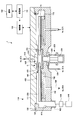
処理容器4の下端の開口部を通して、半導体ウエハWが複数段に載置される石英製のウエハボート12が搬入出される。本実施形態において、ウエハボート12の支柱12Aには、例えば50〜100枚の直径が300mmのウエハWを略等ピッチで多段に支持するための溝(不図示)が形成されている。 Through the opening at the lower end of the processing container 4, a quartz wafer boat 12 on which the semiconductor wafers W are placed in a plurality of stages is carried in and out. In the present embodiment, grooves (not shown) for supporting, for example, 50 to 100 wafers W having a diameter of 300 mm in multiple stages at a substantially equal pitch are formed in the support 12A of the wafer boat 12.
また、図7に示すとおり、凸状部400の周方向中央部には、回転テーブル200の半径方向に沿って延びる溝部430が形成されており、ここに上述の分離ガスノズル420が収容されている。もう一つの凸状部400にも同様に溝部430が形成され、ここに分離ガスノズル410が収容されている。分離ガスノズル420からN2ガスが供給されると、このN2ガスは、分離空間Hを通して空間481及び空間482へ向かって流れる。このとき、分離空間Hの容積は空間481及び482の容積よりも小さいため、N2ガスにより分離空間Hの圧力を空間481及び482の圧力に比べて高くすることができる。すなわち、空間481及び482の間において、分離空間Hは圧力障壁を提供することができる。しかも、分離空間Hから空間481及び482へ流れ出るN2ガスは、第1の処理領域P1へ供給され、凸状部400に向かって流れるTEMAZガス及び/又はTMAガスと、第2の領域P2へ供給され、凸状部400に向かって流れるO3ガスとに対するカウンターフローとして働く。したがって、第1の処理領域P1のTEMAZガス及び/又はTMAガスと、第2の領域P2のO3ガスとを分離空間Hにより確実に分離することができ、よって、真空容器110内においてTEMAZガス及び/又はTMAガスとO3ガスとが混合して反応することが抑制される。
Further, as shown in FIG. 7, a groove portion 430 extending along the radial direction of the
また、図4に示すように、真空容器110の天板111の中心部には分離ガス供給管510が接続されていて、天板111とコア部210との間の空間520に分離ガスであるN2ガスを供給するように構成されている。この空間520に供給された分離ガスは、突出部500と回転テーブル200との狭い空間530を介して回転テーブル200のウエハ載置領域側の表面に沿って周縁に向けて吐出される。空間530は、分離ガスにより空間481及び空間482よりも高い圧力に維持され得る。したがって、空間530により、第1の処理領域P1に供給されるTEMAZガス及び/又はTMAガスと、第2の処理領域P2に供給されるO3ガスとが、中心領域Cを通って混合することが抑制される。すなわち、空間530(又は中心領域C)は分離空間H(又は分離領域D)と同様に機能することができる。
As shown in FIG. 4, a separation
続いてゲートバルブを閉じ、真空ポンプ640により真空容器110を最高到達真空度まで排気した後、分離ガスノズル410、420から分離ガスであるN2ガスを所定の流量で吐出し、分離ガス供給管510及びパージガス供給管720からもN2ガスを所定の流量で吐出する。これに伴い、圧力調整器650により真空容器110内を予め設定した処理圧力に調整する。次いで、回転テーブル200を時計回りに例えば最大で240rpmの回転速度で回転させながら、ヒータユニット700によりウエハWを例えば250℃から350℃までの範囲の温度に加熱する。
Subsequently, after closing the gate valve and evacuating the
TEMAZガスとO3ガスとが同時に供給される間、回転テーブル200の回転によりウエハWが第1の処理領域P1を通過すると、ウエハWがTEMAZガスに晒され(ステップS1(図3)、ウエハWの表面にTEMAZガスが吸着し、第2の処理領域Pを通過すると、ウエハWがO3ガスに晒され(ステップS2(図3)、ウエハWの表面に吸着したTEMAZガスがO3ガスにより酸化される。これにより、ウエハWの表面にZrO膜が成膜される。以下、所望の膜厚を有するZrO膜が形成されるまで所定の回数だけ回転テーブル200を回転し(ステップS3)、TEMAZガスとO3ガスとの供給を停止することにより、第1のZrO膜の成膜を終了する。
While the TEMAZ gas and the O 3 gas are supplied simultaneously, when the wafer W passes through the first processing region P1 by the rotation of the
続けて、反応ガスノズル310からTMAガスを供給する。このとき、反応ガスノズル320からは、O3ガスも他の反応性ガスも供給しない。ただし、反応ガスノズル320からArやHeなどの希ガスや窒素ガスなどの不活性ガスを流しても良い。ここで、回転テーブル200の回転により第1の処理領域P1をウエハWが通過すると、ウエハW(第1のZrO膜)の表面にTMAガスが吸着する。これにより、第1のZrO膜の表面には、TEMAZガス及びTMAガスが吸着していることとなる。
Subsequently, TMA gas is supplied from the reaction gas nozzle 310. At this time, neither the O 3 gas nor other reactive gas is supplied from the reactive gas nozzle 320. However, an inert gas such as a rare gas such as Ar or He or a nitrogen gas may be allowed to flow from the reaction gas nozzle 320. Here, when the wafer W passes through the first processing region P1 by the rotation of the
次に、反応ガスノズル310からのTMAガスの供給を停止し、反応ガスノズル320からO3ガスを真空容器110(第2の処理領域P2)に供給する。ここで、ウエハWが第2の処理領域P2に至ると、ウエハWがO3ガスに晒され(ステップS6(図3))、ウエハWの表面に吸着したTEMAZガス及びTMAガスがO3ガスにより酸化される。そして、回転テーブル200の回転によってウエハWが第2の処理領域P2を複数回通過することにより、ウエハWの表面に吸着したほぼ全てのTEMAZガス及びTMAガスが酸化され、ウエハW(第1のZrO膜)の表面全体にZrAlO膜が成膜される。
Next, the supply of the TMA gas from the reaction gas nozzle 310 is stopped, and the O 3 gas is supplied from the reaction gas nozzle 320 to the vacuum vessel 110 (second processing region P2). Here, when the wafer W reaches the second processing region P2, the wafer W is exposed to the O 3 gas (step S6 (FIG. 3)), and the TEMAZ gas and the TMA gas adsorbed on the surface of the wafer W are the O 3 gas. It is oxidized by. Then, when the wafer W passes through the second processing region P2 a plurality of times by the rotation of the
以下、上述の第1のZrO膜の成膜の手順と同様の手順が行われ(ステップS7からS9)、第2のZrO膜が成膜される。この後、真空容器110へのガスの供給が停止され、回転テーブル200の回転が停止され、真空容器110内にウエハWを搬入したときの手順と逆の手順により、真空容器110内からウエハWが搬出される。これにより成膜工程が終了する。
Thereafter, the same procedure as that for forming the first ZrO film is performed (steps S7 to S9), and the second ZrO film is formed. Thereafter, the supply of gas to the
Claims (8)
前記第1の金属化合物の膜が成膜された前記基板を、前記第1の原料ガスに晒し、前記第1の金属化合物の膜に前記第1の原料ガスを吸着させる吸着ステップと、
前記第1の原料ガスが吸着された前記基板を、第2の金属を含有する第2の原料ガスに晒し、当該基板を、前記第2の原料ガスと反応する前記反応ガスに晒す第2のサイクルを行って第2の金属化合物の膜を前記基板に成膜する第2の成膜ステップと
を含む成膜方法。 The substrate is exposed to a first source gas containing a first metal, and the substrate is exposed to a reaction gas that reacts with the first source gas to perform a first cycle to form a film of the first metal compound. A first film forming step of forming a film on a substrate;
An adsorption step of exposing the substrate on which the first metal compound film is formed to the first source gas and adsorbing the first source gas to the first metal compound film;
The substrate on which the first material gas is adsorbed, the second containing a second metal exposed to the source gas, the substrate, the reaction gas to the exposed second which reacts with said second material gas And a second film forming step of forming a second metal compound film on the substrate by performing a cycle.
Priority Applications (4)
| Application Number | Priority Date | Filing Date | Title |
|---|---|---|---|
| JP2012153407A JP2014017354A (en) | 2012-07-09 | 2012-07-09 | Deposition method |
| TW102124317A TW201416481A (en) | 2012-07-09 | 2013-07-08 | Film deposition method |
| US13/937,070 US9252043B2 (en) | 2012-07-09 | 2013-07-08 | Film deposition method |
| KR1020130079644A KR20140007289A (en) | 2012-07-09 | 2013-07-08 | Film forming method |
Applications Claiming Priority (1)
| Application Number | Priority Date | Filing Date | Title |
|---|---|---|---|
| JP2012153407A JP2014017354A (en) | 2012-07-09 | 2012-07-09 | Deposition method |
Publications (2)
| Publication Number | Publication Date |
|---|---|
| JP2014017354A JP2014017354A (en) | 2014-01-30 |
| JP2014017354A5 true JP2014017354A5 (en) | 2015-01-29 |
Family
ID=49878830
Family Applications (1)
| Application Number | Title | Priority Date | Filing Date |
|---|---|---|---|
| JP2012153407A Pending JP2014017354A (en) | 2012-07-09 | 2012-07-09 | Deposition method |
Country Status (4)
| Country | Link |
|---|---|
| US (1) | US9252043B2 (en) |
| JP (1) | JP2014017354A (en) |
| KR (1) | KR20140007289A (en) |
| TW (1) | TW201416481A (en) |
Families Citing this family (4)
| Publication number | Priority date | Publication date | Assignee | Title |
|---|---|---|---|---|
| JP6115244B2 (en) * | 2013-03-28 | 2017-04-19 | 東京エレクトロン株式会社 | Deposition equipment |
| US20150255267A1 (en) * | 2014-03-09 | 2015-09-10 | Tokyo Electron Limited | Atomic Layer Deposition of Aluminum-doped High-k Films |
| JP6793031B2 (en) * | 2016-12-22 | 2020-12-02 | 東京エレクトロン株式会社 | Substrate processing equipment and substrate processing method, and substrate processing system |
| US11462398B2 (en) | 2019-07-17 | 2022-10-04 | International Business Machines Corporation | Ligand selection for ternary oxide thin films |
Family Cites Families (11)
| Publication number | Priority date | Publication date | Assignee | Title |
|---|---|---|---|---|
| US20050227003A1 (en) * | 2004-04-08 | 2005-10-13 | Carlson Chris M | Methods of forming material over substrates |
| KR100728962B1 (en) * | 2004-11-08 | 2007-06-15 | 주식회사 하이닉스반도체 | Capacitor of semiconductor device with zrconium oxide and method of manufacturing the same |
| KR100670747B1 (en) * | 2005-11-28 | 2007-01-17 | 주식회사 하이닉스반도체 | Method for manufacturing capacitor in semiconductor device |
| JP2007266464A (en) * | 2006-03-29 | 2007-10-11 | Hitachi Ltd | Manufacturing method of semiconductor integrated circuit device |
| JPWO2008108128A1 (en) | 2007-03-08 | 2010-06-10 | 日本電気株式会社 | Dielectric, capacitor using dielectric, semiconductor device using dielectric, and method for manufacturing dielectric |
| JP5270476B2 (en) | 2009-07-07 | 2013-08-21 | 株式会社日立国際電気 | Semiconductor device manufacturing method and substrate processing apparatus |
| JP4988902B2 (en) * | 2009-07-31 | 2012-08-01 | 株式会社日立国際電気 | Semiconductor device manufacturing method and substrate processing apparatus |
| US8501268B2 (en) * | 2010-03-09 | 2013-08-06 | Micron Technology, Inc. | Methods of forming material over a substrate and methods of forming capacitors |
| JP2012059834A (en) * | 2010-09-07 | 2012-03-22 | Hitachi Kokusai Electric Inc | Method for manufacturing semiconductor device |
| JP5587716B2 (en) * | 2010-09-27 | 2014-09-10 | マイクロンメモリジャパン株式会社 | Semiconductor device, manufacturing method thereof, and adsorption site blocking atomic layer deposition method |
| JP2012124322A (en) * | 2010-12-08 | 2012-06-28 | Elpida Memory Inc | Method of manufacturing semiconductor storage |
-
2012
- 2012-07-09 JP JP2012153407A patent/JP2014017354A/en active Pending
-
2013
- 2013-07-08 US US13/937,070 patent/US9252043B2/en not_active Expired - Fee Related
- 2013-07-08 KR KR1020130079644A patent/KR20140007289A/en not_active Application Discontinuation
- 2013-07-08 TW TW102124317A patent/TW201416481A/en unknown
Similar Documents
| Publication | Publication Date | Title |
|---|---|---|
| TWI506159B (en) | Film deposition apparatus | |
| TWI494459B (en) | Film deposition apparatus, film deposition method, and storage medium | |
| TWI542723B (en) | The method of manufacturing a semiconductor device, a substrate processing apparatus and a recording medium | |
| JP5310283B2 (en) | Film forming method, film forming apparatus, substrate processing apparatus, and storage medium | |
| JP5375853B2 (en) | Film forming apparatus, film forming method, and storage medium | |
| JP2010126797A (en) | Film deposition system, semiconductor fabrication apparatus, susceptor for use in the same, program and computer readable storage medium | |
| KR101695511B1 (en) | Method for depositing a film | |
| US8962495B2 (en) | Film deposition method | |
| JP2010073822A (en) | Film deposition apparatus, film deposition method, program and computer readable storage medium | |
| US9136133B2 (en) | Method of depositing film | |
| JP2013048227A (en) | Shower head device and deposition device | |
| JP6685216B2 (en) | Film forming apparatus, film forming method, program, and computer-readable storage medium | |
| JP2010135510A (en) | Depositing device | |
| JP2006286716A (en) | Method of manufacturing semiconductor device | |
| JP6010451B2 (en) | Deposition method | |
| JP2014017354A5 (en) | ||
| KR101734779B1 (en) | Method for depositing a film | |
| US20170241018A1 (en) | Film deposition apparatus, film deposition method and computer readable medium | |
| JP2016141845A (en) | Method of making exhaust pipe harmless and film deposition apparatus | |
| US20180258527A1 (en) | Film Forming Apparatus | |
| JP6096955B2 (en) | Deposition method | |
| JP6906439B2 (en) | Film formation method | |
| JP5276386B2 (en) | Film forming apparatus, film forming method, program for causing film forming apparatus to execute film forming method, and computer-readable storage medium storing the same |