JP2014010212A - Liquid crystal display device - Google Patents
Liquid crystal display device Download PDFInfo
- Publication number
- JP2014010212A JP2014010212A JP2012145125A JP2012145125A JP2014010212A JP 2014010212 A JP2014010212 A JP 2014010212A JP 2012145125 A JP2012145125 A JP 2012145125A JP 2012145125 A JP2012145125 A JP 2012145125A JP 2014010212 A JP2014010212 A JP 2014010212A
- Authority
- JP
- Japan
- Prior art keywords
- liquid crystal
- crystal display
- writing
- video signal
- video
- Prior art date
- Legal status (The legal status is an assumption and is not a legal conclusion. Google has not performed a legal analysis and makes no representation as to the accuracy of the status listed.)
- Pending
Links
Images


Abstract
Description
本発明の実施形態は、液晶表示装置に関する。 Embodiments described herein relate generally to a liquid crystal display device.
液晶表示装置は、軽量、薄型、低消費電力などの特徴を生かして、パーソナルコンピュータなどのOA機器やテレビなどの表示装置として各種分野で利用されている。近年では、液晶表示装置は、携帯電話などの携帯端末機器や、カーナビゲーション装置、ゲーム機などの表示装置としても利用されている。 Liquid crystal display devices are utilized in various fields as display devices for OA equipment such as personal computers and televisions, taking advantage of features such as light weight, thinness, and low power consumption. In recent years, liquid crystal display devices are also used as mobile terminal devices such as mobile phones, display devices such as car navigation devices and game machines.
例えば、特許文献1によれば、OCB(Optically Compensated Bend)型の液晶表示パネルの駆動手法として、1フレーム期間において、黒映像信号を書き込む黒書込期間と、映像信号を書き込む映像書込期間と、書き込んだ映像信号を保持する映像保持期間との順序に駆動制御する駆動手法(ABC駆動法)が開示されている。このような駆動手法では、1フレーム期間の最初に黒映像が書き込まれることにより液晶分子の逆転移を防止できるとともに鮮明な画像を得ることができ、また、映像保持期間においてバックライトを点灯させるため、映像にちらつき等が起こりにくいといった利点がある。
For example, according to
本実施形態の目的は、表示品位の良好な液晶表示装置を提供することにある。 An object of the present embodiment is to provide a liquid crystal display device with good display quality.
本実施形態によれば、
複数のラインで構成された画面を有するOCB型の液晶表示パネルと、1フレーム期間において、前記液晶表示パネルに黒映像信号を書き込む黒書込期間と、前記黒書込期間に続いて前記液晶表示パネルに映像信号を書き込む映像書込期間と、前記映像書込期間に続いて書き込んだ映像信号を保持する映像保持期間との順序に駆動制御する制御手段と、1フレーム期間において、少なくとも前記映像保持期間に点灯し、前記液晶表示パネルを照明する照明手段と、を備え、前記制御手段は、前記映像書込期間において、前記液晶表示パネルにおける画面中央のラインから画面上側及び画面下側のラインに向かって順次映像信号を書き込むことを特徴とする液晶表示装置が提供される。
According to this embodiment,
An OCB type liquid crystal display panel having a screen composed of a plurality of lines, a black writing period for writing a black video signal to the liquid crystal display panel in one frame period, and the liquid crystal display following the black writing period Control means for driving and controlling in order of a video writing period for writing a video signal to the panel and a video holding period for holding the video signal written following the video writing period, and at least the video holding in one frame period Lighting means for illuminating the liquid crystal display panel during the period, and the control means from the center line of the screen in the liquid crystal display panel to the upper and lower screen lines in the video writing period. A liquid crystal display device is provided in which video signals are sequentially written.
また、本実施形態によれば、
複数のラインで構成された画面を有するOCB型の液晶表示パネルと、1フレーム期間において、前記液晶表示パネルに黒映像信号を書き込む黒書込期間と、前記黒書込期間に続いて前記液晶表示パネルに映像信号を書き込む映像書込期間と、前記映像書込期間に続いて書き込んだ映像信号を保持する映像保持期間との順序に駆動制御する制御手段と、1フレーム期間において、少なくとも前記映像保持期間に点灯し、前記液晶表示パネルを照明する照明手段と、を備え、前記制御手段は、前記映像書込期間において、前記液晶表示パネルにおける画面上側及び画面下側のラインから画面中央のラインに向かって順次映像信号を書き込むことを特徴とする液晶表示装置が提供される。
Moreover, according to this embodiment,
An OCB type liquid crystal display panel having a screen composed of a plurality of lines, a black writing period for writing a black video signal to the liquid crystal display panel in one frame period, and the liquid crystal display following the black writing period Control means for driving and controlling in order of a video writing period for writing a video signal to the panel and a video holding period for holding the video signal written following the video writing period, and at least the video holding in one frame period Illuminating means that illuminates the liquid crystal display panel during the period, and the control means changes the lines from the upper and lower screen lines of the liquid crystal display panel to the center line of the screen during the video writing period. A liquid crystal display device is provided in which video signals are sequentially written.
以下、本実施形態に係る液晶表示装置について図面を参照して説明する。 Hereinafter, the liquid crystal display device according to the present embodiment will be described with reference to the drawings.
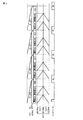
図1は、本実施形態における液晶表示装置の構成を概略的に示す図である。すなわち、この液晶表示装置は、アクティブマトリクスタイプの液晶表示装置であって、OCB型の液晶表示パネルLPNと、液晶表示パネルLPNの駆動を制御する制御手段として機能する制御回路CNTと、液晶表示パネルLPNを照明する照明手段として機能するバックライトBLと、を備えている。 FIG. 1 is a diagram schematically showing a configuration of a liquid crystal display device according to the present embodiment. That is, this liquid crystal display device is an active matrix type liquid crystal display device, which is an OCB type liquid crystal display panel LPN, a control circuit CNT that functions as a control means for controlling driving of the liquid crystal display panel LPN, and a liquid crystal display panel And a backlight BL that functions as illumination means for illuminating the LPN.
液晶表示パネルLPNは、バックライトBLからのバックライト光を選択的に透過して画像を表示する透過型である。この液晶表示パネルLPNは、一対の基板、すなわちアレイ基板ARと、アレイ基板ARに対向して配置された対向基板CTと、を備えている。これらのアレイ基板ARと対向基板CTとは、図示しないシール材によって貼り合わせられている。このような液晶表示パネルLPNは、複数のラインで構成された画面DSPを有している。この画面DSPは、画像を表示するアクティブエリアに対応し、m×n個のマトリクス状に配置された複数の画素PXによって構成されている(但し、m及びnは正の整数である)。なお、図1においては、簡略化のため、1画素のみを図示している。 The liquid crystal display panel LPN is a transmissive type that selectively transmits backlight light from the backlight BL and displays an image. The liquid crystal display panel LPN includes a pair of substrates, that is, an array substrate AR, and a counter substrate CT arranged to face the array substrate AR. The array substrate AR and the counter substrate CT are bonded together by a sealing material (not shown). Such a liquid crystal display panel LPN has a screen DSP composed of a plurality of lines. This screen DSP corresponds to an active area for displaying an image, and is composed of a plurality of pixels PX arranged in a matrix of m × n (where m and n are positive integers). In FIG. 1, only one pixel is shown for the sake of simplicity.
アレイ基板ARは、第1方向D1に沿ってそれぞれ延出したn本のゲート線Y(Y1〜Yn)、各ゲート線Yと交差するように第2方向D2に沿ってそれぞれ延出したm本のソース線X(X1〜Xm)、各画素PXに配置されたm×n個のスイッチング素子W、各画素PXに配置されスイッチング素子Wに接続されたm×n個の画素電極EPなどを備えている。 The array substrate AR includes n gate lines Y (Y1 to Yn) extending along the first direction D1, and m gate lines Y extending along the second direction D2 so as to intersect the gate lines Y, respectively. Source line X (X1 to Xm), m × n switching elements W arranged in each pixel PX, m × n pixel electrodes EP arranged in each pixel PX and connected to the switching element W, and the like. ing.
スイッチング素子Wは、例えば、薄膜トランジスタ(TFT)によって構成されている。スイッチング素子Wのゲート電極WGは、ゲート線Yに電気的に接続されている(あるいは、ゲート電極WGはゲート線Yと一体的に形成されている)。スイッチング素子Wのソース電極WSは、ソース線Xに電気的に接続されている(あるいは、ソース電極WSはソース線Xと一体に形成されている)。スイッチング素子Wのドレイン電極WDは、画素電極EPに電気的に接続されている。 The switching element W is configured by, for example, a thin film transistor (TFT). The gate electrode WG of the switching element W is electrically connected to the gate line Y (or the gate electrode WG is formed integrally with the gate line Y). The source electrode WS of the switching element W is electrically connected to the source line X (or the source electrode WS is formed integrally with the source line X). The drain electrode WD of the switching element W is electrically connected to the pixel electrode EP.
n本のゲート線Yは、それぞれゲートドライバYDに接続されている。このゲートドライバYDは、制御回路CNTによる制御に基づいてn本のゲート線Yに走査信号を供給する。また、m本のソース線Xは、それぞれソースドライバXDに接続されている。このソースドライバXDは、制御回路CNTによる制御に基づいてm本のソース線Xに映像信号(黒映像信号を含む)を供給する。なお、これらのゲートドライバYD及びソースドライバXDも本実施形態の制御手段の一部を構成する。 Each of the n gate lines Y is connected to a gate driver YD. The gate driver YD supplies a scanning signal to the n gate lines Y based on control by the control circuit CNT. The m source lines X are connected to the source driver XD, respectively. The source driver XD supplies video signals (including black video signals) to the m source lines X based on control by the control circuit CNT. Note that these gate driver YD and source driver XD also constitute part of the control means of the present embodiment.
一方、対向基板CTは、対向電極ETなどを備えている。この対向電極ETは、複数の画素PXに共通である。つまり、対向電極ETは、各画素PXの画素電極EPと向かい合っている。 On the other hand, the counter substrate CT includes a counter electrode ET and the like. The counter electrode ET is common to the plurality of pixels PX. That is, the counter electrode ET faces the pixel electrode EP of each pixel PX.
なお、図1においては、画面DSPの一画素PXのみを図示しているが、m×n個の画素PXの全てが同一構造である。すなわち、第1方向D1に沿って同一構造の画素PXがm個並んで配置されるとともに、第2方向D2に沿って同一構造の画素PXがn個並んで配置されている。画面DSPを構成する1ラインとは、第1方向D1に並んだm個の画素PXによって構成されるものである。1ラインの各画素PXに配置されたスイッチング素子Wのゲート電極WGは、同一のゲート線Yに接続されている。このため、スイッチング素子Wをオンさせる走査信号がゲート線Yに供給された場合には、1ラインのm個の画素PXへの映像信号の書き込みが可能となる。 In FIG. 1, only one pixel PX of the screen DSP is shown, but all m × n pixels PX have the same structure. That is, m pixels PX having the same structure are arranged along the first direction D1, and n pixels PX having the same structure are arranged along the second direction D2. One line constituting the screen DSP is constituted by m pixels PX arranged in the first direction D1. The gate electrodes WG of the switching elements W arranged in each line of pixels PX are connected to the same gate line Y. Therefore, when the scanning signal for turning on the switching element W is supplied to the gate line Y, the video signal can be written to the m pixels PX in one line.
バックライトBLは、液晶表示パネルLPNの背面側であるアレイ基板ARと向かい合う側に配置されている。つまり、このバックライトBLは、液晶表示パネルLPNをアレイ基板ARの側から照明する。このようなバックライトBLとしては、種々の形態が適用可能であり、また、光源として発光ダイオードを利用したものや冷陰極管を利用したものなどのいずれでも適用可能であり、詳細な構造については説明を省略する。 The backlight BL is disposed on the side facing the array substrate AR, which is the back side of the liquid crystal display panel LPN. That is, the backlight BL illuminates the liquid crystal display panel LPN from the array substrate AR side. As such a backlight BL, various forms can be applied, and any one using a light-emitting diode or a cold cathode tube as a light source can be applied. Description is omitted.
制御回路CNTは、タイミングコントローラTC、フレームメモリFM、バックライト制御回路BC、液晶駆動回路LCなどを有している。 The control circuit CNT includes a timing controller TC, a frame memory FM, a backlight control circuit BC, a liquid crystal driving circuit LC, and the like.
タイミングコントローラTCは、同期信号に基づいてフレームメモリFMにおける映像信号の記憶及び読み出しのタイミングを制御するのに必要な制御信号を生成する。また、このタイミングコントローラTCは、バックライト制御回路BCに対してバックライトBLの点灯及び消灯のタイミングを制御するのに必要な制御信号を生成する。さらに、このタイミングコントローラTCは、液晶駆動回路LCに対して液晶表示パネルLPNの各画素PXへの映像信号の書込のタイミングを制御するのに必要な制御信号を生成する。 The timing controller TC generates a control signal necessary for controlling the timing of storing and reading the video signal in the frame memory FM based on the synchronization signal. Further, the timing controller TC generates a control signal necessary for controlling the timing of turning on and off the backlight BL for the backlight control circuit BC. Further, the timing controller TC generates a control signal necessary for controlling the timing of writing the video signal to each pixel PX of the liquid crystal display panel LPN with respect to the liquid crystal driving circuit LC.
フレームメモリFMは、タイミングコントローラTCからの制御信号に基づいて、供給された映像信号を一時的に記憶する。このフレームメモリFMは、ランダムアクセスが可能なランダム・アクセス・メモリとして構成されることが望ましい。また、このフレームメモリFMは、例えば1フレーム分の映像信号を記憶した後、この記憶した映像信号が読み出されるまでに次フレームの映像信号が供給される場合があるため、約2フレーム分の記憶容量を有することが望ましい。 The frame memory FM temporarily stores the supplied video signal based on the control signal from the timing controller TC. The frame memory FM is preferably configured as a random access memory capable of random access. In addition, since the frame memory FM stores, for example, a video signal for one frame and then the video signal of the next frame may be supplied before the stored video signal is read out, the frame memory FM stores about two frames. It is desirable to have a capacity.
バックライト制御回路BCは、タイミングコントローラTCからの制御信号に基づいて、バックライトBLの点灯及び消灯を制御する。 The backlight control circuit BC controls lighting and extinguishing of the backlight BL based on a control signal from the timing controller TC.
液晶駆動回路LCは、ゲートドライバYDから各ゲート線Yに走査信号を供給させるのに必要な走査制御信号をゲートドライバYDに供給する。また、この液晶駆動回路LCは、フレームメモリFMに記憶された映像信号を所定の順に読み出し、必要に応じて所定の処理を施した後に、1ラインの画素PX分ずつソースドライバXDに供給する。また、この液晶駆動回路LCは、黒映像信号を生成し、1ラインの画素PX分ずつソースドライバXDに供給する。 The liquid crystal driving circuit LC supplies the gate driver YD with a scanning control signal necessary for supplying a scanning signal from the gate driver YD to each gate line Y. In addition, the liquid crystal driving circuit LC reads out the video signals stored in the frame memory FM in a predetermined order, performs predetermined processing as necessary, and supplies the video signals to the source driver XD for each pixel PX. The liquid crystal driving circuit LC generates a black video signal and supplies it to the source driver XD for each line of pixels PX.
次に、OCB型の液晶表示パネルLPNの構造について、以下により詳細に説明する。 Next, the structure of the OCB type liquid crystal display panel LPN will be described in more detail below.
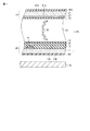
図2は、図1に示した液晶表示パネルLPNの概略断面図である。 FIG. 2 is a schematic cross-sectional view of the liquid crystal display panel LPN shown in FIG.
液晶表示パネルLPNのアレイ基板ARは、ガラス板などの光透過性を有する絶縁基板11を用いて形成されている。このアレイ基板ARは、絶縁基板11の第1面11Aつまり対向基板CTと向かい合う側に、スイッチング素子W、絶縁膜12、画素電極EP、画素電極EPを覆う第1配向膜13などを備えている。画素電極EPは、インジウム・ティン・オキサイド(ITO)やインジウム・ジンク・オキサイド(IZO)などの光透過性を有する導電材料によって形成されている。
The array substrate AR of the liquid crystal display panel LPN is formed using a light-transmitting insulating
液晶表示パネルLPNの対向基板CTは、ガラス板などの光透過性を有する絶縁基板21を用いて形成されている。この対向基板CTは、絶縁基板21の第1面21Aつまりアレイ基板ARと向かい合う側に、対向電極ET、対向電極ETを覆う第2配向膜22などを備えている。対向電極ETは、例えばITOなどの光透過性を有する導電材料によって形成されている。なお、対向基板CTは、必要に応じて、ブラックマトリクスやカラーフィルタ層、オーバーコート層などを備えていても良い。
The counter substrate CT of the liquid crystal display panel LPN is formed using an insulating
上述したような構成のアレイ基板ARと対向基板CTとは、画素電極EPと対向電極ETとを対向させた状態で配置され、これらの間に図示しないスペーサ(例えば、一方の基板に一体的に形成された柱状スペーサ)を介して所定のセルギャップを形成する。これらのアレイ基板ARと対向基板CTとの間に形成されたセルギャップには、液晶層LQが保持されている。 The array substrate AR and the counter substrate CT configured as described above are arranged in a state where the pixel electrode EP and the counter electrode ET are opposed to each other, and a spacer (not shown) (for example, integrally with one substrate) is interposed therebetween. A predetermined cell gap is formed through the formed columnar spacers. A liquid crystal layer LQ is held in the cell gap formed between the array substrate AR and the counter substrate CT.
液晶層LQは、正の誘電率異方性を有するとともに光学的に正の一軸性を有する液晶分子31を含む液晶組成物によって構成されている。この液晶層LQにおいては、液晶層LQに所定の電圧(転移電圧)を印加した所定の表示状態において、液晶分子31は、アレイ基板ARと対向基板CTとの間でベンド配向している。 The liquid crystal layer LQ is composed of a liquid crystal composition including liquid crystal molecules 31 having positive dielectric anisotropy and optically positive uniaxiality. In the liquid crystal layer LQ, the liquid crystal molecules 31 are bend-aligned between the array substrate AR and the counter substrate CT in a predetermined display state in which a predetermined voltage (transition voltage) is applied to the liquid crystal layer LQ.
液晶表示パネルLPNの外面には、第1光学補償層OD1及び第2光学補償層OD2がそれぞれ配置されている。これらの第1光学補償素子OD1及び第2光学補償素子OD2は、上述したような液晶表示パネルLPNにおける液晶層LQに電圧を印加した所定の表示状態において、液晶層LQのリタデーションを光学的に補償する機能を有しており、偏光板及び位相差板などを備えて構成されている。 A first optical compensation layer OD1 and a second optical compensation layer OD2 are disposed on the outer surface of the liquid crystal display panel LPN. The first optical compensation element OD1 and the second optical compensation element OD2 optically compensate for retardation of the liquid crystal layer LQ in a predetermined display state in which a voltage is applied to the liquid crystal layer LQ in the liquid crystal display panel LPN as described above. And has a polarizing plate and a retardation plate.
第1光学補償素子OD1は、アレイ基板ARを構成する絶縁基板11の第2面11BつまりバックライトBLと向かい合う面に配置されている。また、第2光学補償素子OD2は、対向基板CTを構成する絶縁基板21の第2面21Bつまり観察側の面に配置されている。
The first optical compensation element OD1 is disposed on the
このようなOCB型の液晶表示パネルLPNにおいては、液晶層LQを保持する第1配向膜13及び第2配向膜22は、互いに平行な方向にラビング処理されている。このような第1配向膜13及び第2配向膜22の作用により、電源投入以前の段階では、液晶分子31は、スプレイ配向している。
In such an OCB type liquid crystal display panel LPN, the
そして、電源投入後、表示動作以前の段階において、初期化処理が行われる。この初期化処理は、液晶層LQに対して転移電圧を印加するものであり、この転移電圧に対応した比較的強い電界により液晶分子31の配向状態をスプレイ配向からベンド配向に転移させる。液晶分子31の配向状態は、表示動作中、ベンド配向に維持されている。 Then, after the power is turned on, an initialization process is performed before the display operation. In this initialization process, a transition voltage is applied to the liquid crystal layer LQ, and the alignment state of the liquid crystal molecules 31 is shifted from the splay alignment to the bend alignment by a relatively strong electric field corresponding to the transition voltage. The alignment state of the liquid crystal molecules 31 is maintained in the bend alignment during the display operation.
表示動作において、液晶層LQに白画像(あるいは最高輝度に対応した階調レベルの画像)を表示するための白表示電圧が印加された際には、液晶層LQのミッドプレーン付近の液晶分子31が基板に略垂直に立ち上がっているのに対してアレイ基板AR及び対向基板CTにそれぞれ近づくにしたがって液晶分子31が基板の法線から傾き、基板近傍の液晶分子31は基板面とほぼ平行な方向に傾いた状態となる。また、液晶層LQに黒画像(あるいは最低輝度に対応した階調レベルの画像)を表示する場合、白表示電圧より高い黒表示電圧(あるいは黒映像信号)が印加された際には、液晶層LQの液晶分子31が略垂直に立ち上がった状態となる。 In the display operation, when a white display voltage for displaying a white image (or an image having a gradation level corresponding to the maximum luminance) is applied to the liquid crystal layer LQ, the liquid crystal molecules 31 near the midplane of the liquid crystal layer LQ. Rises substantially perpendicular to the substrate, but as the array substrate AR and the counter substrate CT approach each other, the liquid crystal molecules 31 are inclined from the normal line of the substrate, and the liquid crystal molecules 31 in the vicinity of the substrate are in a direction substantially parallel to the substrate surface. It will be in a state inclined to. When displaying a black image (or an image having a gradation level corresponding to the lowest luminance) on the liquid crystal layer LQ, when a black display voltage (or black video signal) higher than the white display voltage is applied, the liquid crystal layer The liquid crystal molecules 31 of LQ are brought up in a substantially vertical state.
このようなOCB型の液晶表示パネルLPNにおいては、液晶分子31の配向状態は、スプレイ配向のエネルギーとベンド配向のエネルギーとが拮抗するレベル以下の電圧印加状態や電圧無印加状態が長期間続く場合に、再びベンド配向からスプレイ配向に逆転移してしまう。 In such an OCB type liquid crystal display panel LPN, the alignment state of the liquid crystal molecules 31 is such that a voltage application state or a voltage non-application state below a level at which the splay alignment energy and the bend alignment energy antagonize continues for a long time. Furthermore, the reverse transition from the bend alignment to the splay alignment occurs again.
このため、OCB型の液晶表示パネルLPNでは、この逆転移を防止するために、1フレーム期間内に液晶層LQに黒表示電圧が印加される(黒挿入駆動方式)。これにより、液晶層LQのベンド配向を維持している。 Therefore, in the OCB type liquid crystal display panel LPN, in order to prevent this reverse transition, a black display voltage is applied to the liquid crystal layer LQ within one frame period (black insertion drive method). Thereby, the bend alignment of the liquid crystal layer LQ is maintained.
次に、OCB型の液晶表示パネルLPNに適用可能な駆動手法について図3を参照しながら説明する。 Next, a driving method applicable to the OCB type liquid crystal display panel LPN will be described with reference to FIG.
ここでは、例えば垂直同期信号VSYNCがONしてから一旦OFFした後に再度ONするまでの期間を1フレーム期間とする。この1フレーム期間には、黒書込期間、映像書込期間、映像保持期間(ホールド期間)が含まれる。黒書込期間は、液晶駆動回路LCから液晶表示パネルLPNに供給された黒映像信号を液晶表示パネルLPNの各画素PXに書き込む期間に相当する。映像書込期間は、液晶駆動回路LCから液晶表示パネルLPNに供給された映像信号を液晶表示パネルLPNの各画素PXに書き込む期間に相当する。ホールド期間は、各画素PXに書き込まれた映像信号を保持する期間に相当する。 Here, for example, a period from when the vertical synchronization signal VSYNC is turned on to once being turned off and then turned on again is defined as one frame period. This one frame period includes a black writing period, a video writing period, and a video holding period (holding period). The black writing period corresponds to a period during which the black video signal supplied from the liquid crystal driving circuit LC to the liquid crystal display panel LPN is written to each pixel PX of the liquid crystal display panel LPN. The video writing period corresponds to a period during which a video signal supplied from the liquid crystal driving circuit LC to the liquid crystal display panel LPN is written to each pixel PX of the liquid crystal display panel LPN. The hold period corresponds to a period for holding the video signal written in each pixel PX.
例えば、画面DSPが1200本のラインによって構成されている場合、まず、同期信号VSYNCがOFFしたタイミングで画面DSPの最上部に位置するライン0001への黒映像信号の書込が開始される。その後、ライン0002からライン1200へと画面DSPの下部のラインに順次黒映像信号の書込が行われる(黒書込期間)。
For example, when the screen DSP is composed of 1200 lines, first, writing of a black video signal to the
画面DSPのすべてのラインへの黒映像信号の書込が完了した後、画面DSPの最上部のライン0001への映像信号の書込が開始される。ライン0001の各画素PXに書き込まれた映像信号は、保持される。ライン0001への映像信号の書込が終了した後、ライン0002からライン1200へと画面DSPの下部のラインに順次映像信号の書込が行われる(映像書込期間)。各ラインの画素PXに書き込まれた映像信号はそれぞれ保持される。
After the writing of the black video signal to all the lines of the screen DSP is completed, the writing of the video signal to the
画面DSPのすべてのラインへの映像信号の書込が完了したタイミングで、バックライトBLが点灯する。このバックライトBLは、黒書込期間及び映像書込期間においては消灯している。 The backlight BL is turned on at the timing when the writing of the video signal to all the lines of the screen DSP is completed. The backlight BL is turned off during the black writing period and the video writing period.
一方で、このような駆動手法の場合、画面DSPを構成する全てのラインへの映像書込が完了した後にバックライトBLを点灯するため、映像信号の書込が完了してからバックライトBLが点灯されるまでの時間が画面DSPの上部と下部とで相違している。すなわち、画面DSPの上部のラインについては、映像信号の書込が完了してから十分な時間が経過した後にバックライトBLが点灯するのに対して、画面DSPの下部のラインについては、映像信号の書込が完了した直後にバックライトBLが点灯する。 On the other hand, in the case of such a driving method, since the backlight BL is turned on after the video writing to all the lines constituting the screen DSP is completed, the backlight BL is turned on after the video signal writing is completed. The time until lighting is different between the upper part and the lower part of the screen DSP. That is, for the upper line of the screen DSP, the backlight BL is turned on after a sufficient time has elapsed since the completion of the writing of the video signal, whereas for the lower line of the screen DSP, the video signal Immediately after the writing is completed, the backlight BL is turned on.
図4に示すように、例えば、画面DSPのライン0001からライン0300付近までの上部UPにおいては、映像信号の書込が完了してからバックライトBLが点灯するまでの間に、液晶分子31の応答速度よりも十分に長い時間が経過している。このため、液晶分子31の転移が完了した状態でバックライトBLが点灯する。したがって、液晶表示パネルLPNにおいては、映像信号に対応した透過率が得られる。
As shown in FIG. 4, for example, in the upper part UP of the screen DSP from the
一方で、例えば、画面DSPのライン0901からライン1200付近までの下部LWにおいては、映像信号の書込が完了してからバックライトBLが点灯するまでの間に、液晶分子31の応答速度よりも十分に長い時間が経過していない。このため、液晶分子31の転移が完了する前の状態でバックライトBLが点灯することがある。したがって、液晶表示パネルLPNにおいては、映像信号に対応した透過率が得られない場合がある。
On the other hand, for example, in the lower LW from the line 0901 to the vicinity of the
画面DSPの全体で白色を表示する場合、上部UPは下部LWよりも明るくなる。このように、画面DSPにおいて、上下で輝度の分布が非対称となる現象を改善することが要求される。 When white is displayed on the entire screen DSP, the upper UP is brighter than the lower LW. As described above, in the screen DSP, it is required to improve the phenomenon in which the luminance distribution is asymmetric in the vertical direction.
そこで、本実施形態においては、面内DSPにおける輝度分布を上下対称とする最適な駆動手法を提供するものである。 In view of this, the present embodiment provides an optimum driving method in which the luminance distribution in the in-plane DSP is vertically symmetric.
図5は、第1実施形態のOCB型の液晶表示パネルLPNに適用可能な第1駆動手法を説明するための図である。なお、ここでは、主として映像書込期間を詳細に説明し、黒書込期間や映像信号保持期間については詳細な説明を省略する。 FIG. 5 is a diagram for explaining a first driving method applicable to the OCB type liquid crystal display panel LPN of the first embodiment. Here, the video writing period is mainly described in detail, and detailed description of the black writing period and the video signal holding period is omitted.
この第1駆動手法では、1フレーム期間の映像書込期間において、液晶表示パネルLPNにおける画面DSPの中央のラインから画面DSPの上側及び下側のラインに向かって順次映像信号を書き込むことを特徴とするものである。例えば、画面DSPが1200本のラインによって構成されている場合、ライン0001からライン0600までが画面DSPの上側半分の第1領域DSP1に相当し、ライン0601からライン1200までが画面DSPの下側半分の第2領域DSP2に相当する。
This first driving method is characterized by sequentially writing video signals from the center line of the screen DSP in the liquid crystal display panel LPN toward the upper and lower lines of the screen DSP in the video writing period of one frame period. To do. For example, when the screen DSP is composed of 1200 lines, the
このような画面DSPの構成において、画面DSPの第1領域DSP1では、ライン0600への映像信号の書込を行った後、順次ライン0599、ライン0598…ライン0002、ライン0001へと映像信号の書込を行う。同様に、画面DSPの第2領域DSP2では、ライン0601への映像信号の書込を行った後、順次ライン0602、ライン0603…ライン1199、ライン1200へと映像信号の書込を行う。
In such a configuration of the screen DSP, in the first area DSP1 of the screen DSP, after the video signal is written to the
画面DSPのすべてのラインへの映像信号の書込が完了したタイミングで、バックライトBLが点灯する。このバックライトBLは、黒書込期間及び映像書込期間においては消灯している。 The backlight BL is turned on at the timing when the writing of the video signal to all the lines of the screen DSP is completed. The backlight BL is turned off during the black writing period and the video writing period.
なお、黒書込期間においては、映像書込期間と同一の順序で黒映像信号を書き込んでも良いが、図3を参照して説明したのと同様に、画面DSPのライン0001から下側に向かってライン1200まで順次黒映像信号を書き込んでも良いし、他の手法で黒映像信号を書き込んでも良く、特定の書込順序に制限されるものではない。
In the black writing period, black video signals may be written in the same order as in the video writing period. However, in the same way as described with reference to FIG. Thus, the black video signal may be sequentially written up to the
上述した第1領域DSP1及び第2領域DSP2からなる画面DSPを備えた液晶表示パネルLPNに対して、第1領域DSP1及び第2領域DSP2に映像信号を書き込むためのソースドライバが単一の構成において、より具体的な映像信号の書込動作について説明する。 In the liquid crystal display panel LPN having the screen DSP composed of the first area DSP1 and the second area DSP2, the source driver for writing the video signal in the first area DSP1 and the second area DSP2 has a single configuration. A more specific video signal writing operation will be described.
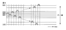
図6は、画面DSPを構成する各ラインに対応したゲート線の走査タイミングを説明するための図である。 FIG. 6 is a diagram for explaining the scanning timing of the gate line corresponding to each line constituting the screen DSP.
例えば、画面DSPが1200本のラインによって構成されている場合、映像書込期間においては、まず、画面DSPの中央に位置するライン0600への映像信号の書込が行われる。その後、ライン0600よりも下側のライン0601への映像信号の書込に続いて、ライン600よりも上側のライン0599への映像信号の書込が行われる。その後は、上側のラインへの映像信号の書込と下側のラインへの映像信号の書込とが交互に行われる(ライン0602→ライン0598→ライン0603→ライン0597…ライン1200→ライン0001)。
For example, when the screen DSP is composed of 1200 lines, first, in the video writing period, the video signal is written to the
なお、上述した第1領域DSP1及び第2領域DSP2からなる画面DSPを備えた液晶表示パネルLPNに対して、第1領域DSP1に映像信号を書き込むための第1ソースドライバと、第2領域DSP2に映像信号を書き込むための第2ソースドライバとを具備した構成においては、第1領域DSP1への映像信号の書込と、第2領域DSP2への映像信号の書込とを同時に行ってもよい。例えば、ライン0600及びライン0601への映像信号の書込や、ライン0599及びライン0602への映像信号の書込などはそれぞれ同時に行ってもよい。このような構成の場合、映像信号の書込時間を短縮することができる。
For the liquid crystal display panel LPN having the screen DSP composed of the first area DSP1 and the second area DSP2, the first source driver for writing the video signal in the first area DSP1 and the second area DSP2 are used. In the configuration including the second source driver for writing the video signal, the writing of the video signal to the first area DSP1 and the writing of the video signal to the second area DSP2 may be performed simultaneously. For example, writing of video signals to the
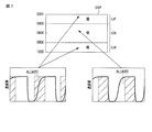
図7は、画面DSPの上部UP、下部LW、中央部CNにおける液晶表示パネルの透過率とバックライトBLの点灯タイミングとの関係を説明するための図である。 FIG. 7 is a diagram for explaining the relationship between the transmittance of the liquid crystal display panel and the lighting timing of the backlight BL in the upper part UP, the lower part LW, and the central part CN of the screen DSP.
例えば、画面DSPの中央部CNのライン0600付近においては、映像信号の書込が完了してからバックライトBLが点灯するまでの間に、液晶分子31の応答速度よりも十分に長い時間が経過している。このため、液晶分子31の転移が完了した状態でバックライトBLが点灯する。したがって、液晶表示パネルLPNにおいては、映像信号に対応した透過率が得られる。
For example, in the vicinity of the
一方で、例えば、画面DSPのライン0001からライン0300付近までの上部UP及びライン0901からライン1200付近までの下部LWにおいては、映像信号の書込が完了してからバックライトBLが点灯するまでの間に、液晶分子31の応答速度よりも十分に長い時間が経過していない。このため、液晶分子31の転移が完了する前の状態でバックライトBLが点灯することがある。したがって、液晶表示パネルLPNにおいては、映像信号に対応した透過率が得られない場合がある。
On the other hand, for example, in the upper UP from the
つまり、画面DSPの中央部CNのラインへの映像信号の書込が完了してからバックライトBLが点灯するまでの時間は、画面DSPの上部UPの側のライン及び画面DSPの下部LWの側のラインへの映像信号の書込が完了してからバックライトBLが点灯するまでの時間より長い。なお、画面DSPの上部UPの側のラインへの映像信号の書込が完了してからバックライトBLが点灯するまでの時間は、画面DSPの下部LWの側のラインへの映像信号の書込が完了してからバックライトBLが点灯するまでの時間と略同等である。 That is, the time from the completion of the writing of the video signal to the line of the center part CN of the screen DSP until the backlight BL is turned on is the line on the upper UP side of the screen DSP and the lower LW side of the screen DSP. This is longer than the time from the completion of the writing of the video signal to the line until the backlight BL is turned on. Note that the time from the completion of the writing of the video signal to the line on the upper side UP of the screen DSP to the lighting of the backlight BL is the writing of the video signal to the line on the lower LW side of the screen DSP. Is substantially the same as the time from when the backlight is completed until the backlight BL is turned on.
このため、画面DSPの各ラインに同一の映像信号、例えば、画面DSPの全体で白色を表示する白色表示電圧が書き込まれた場合、中央部CNでの輝度は、上部UP及び下部LWよりも高くなる。このとき、画面DSPの上部UP及び下部LWにおける輝度は、略同等となる。つまり、第1駆動手法を適用することにより、画面DSPの中央部CNが明るく、この中央部CNを挟んで上側と下側とで対称の輝度分布を形成することができる。したがって、良好な表示品位を得ることが可能となる。 For this reason, when the same video signal, for example, a white display voltage for displaying white in the entire screen DSP, is written to each line of the screen DSP, the luminance at the center CN is higher than that of the upper UP and the lower LW. Become. At this time, the luminance at the upper part UP and the lower part LW of the screen DSP is substantially the same. That is, by applying the first driving method, the central portion CN of the screen DSP is bright, and a symmetrical luminance distribution can be formed on the upper side and the lower side across the central portion CN. Therefore, it is possible to obtain a good display quality.
次に、第2実施形態について説明する。なお、第1実施形態と同一構成については同一の参照符号を付して詳細な説明を省略する。 Next, a second embodiment will be described. In addition, about the same structure as 1st Embodiment, the same referential mark is attached | subjected and detailed description is abbreviate | omitted.
図8は、第2実施形態のOCB型の液晶表示パネルLPNに適用可能な第2駆動手法を説明するための図である。なお、ここでは、主として映像書込期間を詳細に説明し、黒書込期間や映像信号保持期間については詳細な説明を省略する。 FIG. 8 is a diagram for explaining a second driving method applicable to the OCB type liquid crystal display panel LPN of the second embodiment. Here, the video writing period is mainly described in detail, and detailed description of the black writing period and the video signal holding period is omitted.
この第2駆動手法では、1フレーム期間の映像書込期間において、液晶表示パネルLPNにおける画面DSPの上側及び下側のラインから画面DSPの中央のラインに向かって順次映像信号を書き込むことを特徴とするものである。 This second driving method is characterized by sequentially writing video signals from the upper and lower lines of the screen DSP in the liquid crystal display panel LPN toward the center line of the screen DSP in the video writing period of one frame period. To do.
すなわち、画面DSPの第1領域DSP1では、ライン0001への映像信号の書込を行った後、順次ライン0002、ライン0003…ライン0599、ライン0600へと映像信号の書込を行う。同様に、画面DSPの第2領域DSP2では、ライン1200への映像信号の書込を行った後、順次ライン1199、ライン1198…ライン0602、ライン0601へと映像信号の書込を行う。
That is, in the first area DSP1 of the screen DSP, after the video signal is written to the
バックライトBLは、画面DSPのすべてのラインへの映像信号の書込が完了してから所定時間が経過した後に点灯する。すべてのラインへの映像信号の書込が完了してからバックライトBLが点灯するまでの時間は、液晶分子31の応答速度よりも十分に長い時間に設定されている。また、このバックライトBLは、画面DSPの中のラインへの黒書込が開始されるまでの間、点灯していることが望ましい。 The backlight BL is turned on after a predetermined time has elapsed since the completion of the writing of the video signal to all the lines of the screen DSP. The time from when the writing of the video signal to all the lines is completed until the backlight BL is turned on is set to a time sufficiently longer than the response speed of the liquid crystal molecules 31. The backlight BL is preferably lit until black writing to the line in the screen DSP is started.
なお、黒書込期間においては、第1実施形態と同様に、黒映像信号の書込順序については、特定の書込順序に制限されるものではない。 In the black writing period, as in the first embodiment, the writing order of the black video signal is not limited to a specific writing order.
上述した第1領域DSP1及び第2領域DSP2からなる画面DSPを備えた液晶表示パネルLPNに対して、第1領域DSP1及び第2領域DSP2に映像信号を書き込むためのソースドライバXDが単一の構成において、より具体的な映像信号の書込動作について説明する。 A single source driver XD for writing a video signal in the first area DSP1 and the second area DSP2 with respect to the liquid crystal display panel LPN having the screen DSP composed of the first area DSP1 and the second area DSP2 described above. Now, a more specific video signal writing operation will be described.
図9は、画面DSPを構成する各ラインに対応したゲート線の走査タイミングを説明するための図である。 FIG. 9 is a diagram for explaining the scanning timing of the gate line corresponding to each line constituting the screen DSP.
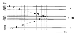
例えば、画面DSPが1200本のラインによって構成されている場合、映像書込期間においては、まず、画面DSPの最上部に位置するライン0001への映像信号の書込が行われる。その後、画面DSPの最下部に位置するライン1200への映像信号の書込が行われる。続いて、ライン0002への映像信号の書込、ライン1199への映像信号の書込、ライン0003への映像信号の書込、ライン1198への映像信号の書込が順次行われる。その後は、同様にして、上側のラインへの映像信号の書込と下側のラインへの映像信号の書込とが交互に行われる(ライン0004→ライン1197→ライン0005→ライン1196…ライン0601→ライン0599→ライン0600)。
For example, when the screen DSP is composed of 1200 lines, first, in the video writing period, the video signal is written to the
なお、上述した第1領域DSP1及び第2領域DSP2からなる画面DSPを備えた液晶表示パネルLPNに対して、第1領域DSP1に映像信号を書き込むための第1ソースドライバと、第2領域DSP2に映像信号を書き込むための第2ソースドライバとを具備した構成においては、第1領域DSP1への映像信号の書込と、第2領域DSP2への映像信号の書込とを同時に行ってもよい。例えば、ライン0001及びライン1200への映像信号の書込や、ライン0002及びライン1199への映像信号の書込などはそれぞれ同時に行ってもよい。このような構成の場合、映像信号の書込時間を短縮することができる。
For the liquid crystal display panel LPN having the screen DSP composed of the first area DSP1 and the second area DSP2, the first source driver for writing the video signal in the first area DSP1 and the second area DSP2 are used. In the configuration including the second source driver for writing the video signal, the writing of the video signal to the first area DSP1 and the writing of the video signal to the second area DSP2 may be performed simultaneously. For example, the writing of video signals to the
図10は、画面DSPの上部UP、下部LW、中央部CNにおける液晶表示パネルの透過率とバックライトBLの点灯タイミングとの関係を説明するための図である。 FIG. 10 is a diagram for explaining the relationship between the transmittance of the liquid crystal display panel and the lighting timing of the backlight BL in the upper part UP, the lower part LW, and the central part CN of the screen DSP.
例えば、画面DSPの中央部CNのライン0600付近においては、映像信号の書込が完了してからバックライトBLが点灯するまでの間に、液晶分子31の応答速度よりも十分に長い時間が経過している。このため、液晶分子31の転移が完了した状態でバックライトBLが点灯する。したがって、液晶表示パネルLPNにおいては、映像信号に対応した透過率が得られる。
For example, in the vicinity of the
一方で、例えば、画面DSPのライン0001からライン0300付近までの上部UP及びライン0901からライン1200付近までの下部LWにおいては、映像信号の書込が完了してからバックライトBLが点灯するまでの間に、液晶分子31の応答速度よりも十分に長い時間が経過しているが、バックライトBLが点灯中に黒書込が開始される。このため、液晶表示パネルLPNにおいては、映像信号に対応した透過率が得られない場合がある。
On the other hand, for example, in the upper UP from the
つまり、画面DSPの中央部CNのラインへの映像信号の書込が完了してからバックライトBLが点灯するまでの時間は、画面DSPの上部UPの側のライン及び画面DSPの下部LWの側のラインへの映像信号の書込が完了してからバックライトBLが点灯するまでの時間より短い。しかも、バックライトBLが点灯している期間において、画面DSPの上部UPの側のライン及び画面DSPの下部LWの側のラインへの黒映像信号の書込が開始される。なお、画面DSPの上部UPの側のラインでの映像信号保持期間中にバックライトBLが点灯している時間は、画面DSPの下部LWの側のラインでの映像信号保持期間中にバックライトBLが点灯している時間と略同等である。 That is, the time from the completion of the writing of the video signal to the line of the center part CN of the screen DSP until the backlight BL is turned on is the line on the upper UP side of the screen DSP and the lower LW side of the screen DSP. This is shorter than the time from the completion of the writing of the video signal to the line until the backlight BL is turned on. In addition, during the period in which the backlight BL is lit, the writing of the black video signal to the upper UP line of the screen DSP and the lower LW side line of the screen DSP is started. Note that the time during which the backlight BL is lit during the video signal holding period in the line on the upper side of the screen DSP is the backlight BL during the video signal holding period in the line on the lower LW side of the screen DSP. Is approximately equivalent to the time when is lit.
このため、画面DSPの各ラインに同一の映像信号、例えば、画面DSPの全体で白色を表示する白色表示電圧が書き込まれた場合、中央部CNでの輝度は、上部UP及び下部LWよりも高くなる。このとき、画面DSPの上部UP及び下部LWにおける輝度は、略同等となる。つまり、第2駆動手法を適用することにより、画面DSPの中央部CNが明るく、この中央部CNを挟んで上側と下側とで対称の輝度分布を形成することができる。したがって、良好な表示品位を得ることが可能となる。 For this reason, when the same video signal, for example, a white display voltage for displaying white in the entire screen DSP, is written to each line of the screen DSP, the luminance at the center CN is higher than that of the upper UP and the lower LW. Become. At this time, the luminance at the upper part UP and the lower part LW of the screen DSP is substantially the same. That is, by applying the second driving method, the central portion CN of the screen DSP is bright, and a symmetrical luminance distribution can be formed on the upper side and the lower side across the central portion CN. Therefore, it is possible to obtain a good display quality.
なお、上記した第1駆動手法と第2駆動手法との選択は、ゲート線の走査に必要な時間が1フレームに対して十分かどうかによって決定され、十分な場合は第1駆動手法が有効であり、不十分の場合は第2駆動手法が有効である。 The selection between the first driving method and the second driving method is determined by whether or not the time required for scanning the gate line is sufficient for one frame. If the time is sufficient, the first driving method is effective. If there is not enough, the second driving method is effective.
以上説明したように、本実施形態によれば、表示品位の良好な液晶表示装置を提供することができる。 As described above, according to this embodiment, it is possible to provide a liquid crystal display device with good display quality.
なお、本発明のいくつかの実施形態を説明したが、これらの実施形態は、例として提示したものであり、発明の範囲を限定することは意図していない。これらの新規な実施形態は、その他の様々な形態で実施されることが可能であり、発明の要旨を逸脱しない範囲で、種々の省略、置き換え、変更を行うことができる。これらの実施形態やその変形は、発明の範囲や要旨に含まれるとともに、特許請求の範囲に記載された発明とその均等の範囲に含まれる。 In addition, although some embodiment of this invention was described, these embodiment is shown as an example and is not intending limiting the range of invention. These novel embodiments can be implemented in various other forms, and various omissions, replacements, and changes can be made without departing from the spirit of the invention. These embodiments and modifications thereof are included in the scope and gist of the invention, and are included in the invention described in the claims and the equivalents thereof.
例えば、上記した液晶表示パネルLPNに対して、スキャンバックライトを組み合わせても良い。すなわち、複数の領域によって構成された画面DSPを備えた液晶表示パネルLPNに対して、各領域に対応して点灯領域が区画されたバックライトBLを用意し、液晶表示パネルLPNの各領域への映像信号の書込→保持の期間に対応してバックライトBLの各点灯領域を順次切り替える構成としても良い。 For example, a scan backlight may be combined with the liquid crystal display panel LPN described above. That is, for a liquid crystal display panel LPN having a screen DSP constituted by a plurality of areas, a backlight BL having a lighting area corresponding to each area is prepared, and each area of the liquid crystal display panel LPN is supplied to each area. A configuration may be adopted in which the lighting regions of the backlight BL are sequentially switched in accordance with the period of writing and holding the video signal.
LPN…液晶表示パネル
AR…アレイ基板 CT…対向基板 LQ…液晶層
DSP…画面 UP…上部 CN…中央部 LW…下部 PX…画素
EP…画素電極 W…スイッチング素子 ET…対向電極
BL…バックライト
LPN ... Liquid crystal display panel AR ... Array substrate CT ... Counter substrate LQ ... Liquid crystal layer DSP ... Screen UP ... Upper CN ... Center portion LW ... Lower PX ... Pixel EP ... Pixel electrode W ... Switching element ET ... Counter electrode BL ... Backlight
Claims (5)
1フレーム期間において、前記液晶表示パネルに黒映像信号を書き込む黒書込期間と、前記黒書込期間に続いて前記液晶表示パネルに映像信号を書き込む映像書込期間と、前記映像書込期間に続いて書き込んだ映像信号を保持する映像保持期間との順序に駆動制御する制御手段と、
1フレーム期間において、少なくとも前記映像保持期間に点灯し、前記液晶表示パネルを照明する照明手段と、を備え、
前記制御手段は、前記映像書込期間において、前記液晶表示パネルにおける画面中央のラインから画面上側及び画面下側のラインに向かって順次映像信号を書き込むことを特徴とする液晶表示装置。 An OCB type liquid crystal display panel having a screen composed of a plurality of lines;
In one frame period, a black writing period for writing a black video signal to the liquid crystal display panel, a video writing period for writing a video signal to the liquid crystal display panel following the black writing period, and a video writing period Control means for driving and controlling in order of the video holding period for holding the written video signal;
Illuminating means that illuminates at least the video holding period and illuminates the liquid crystal display panel in one frame period,
The liquid crystal display device, wherein the control means sequentially writes video signals from the center line of the liquid crystal display panel toward the upper and lower screen lines during the video writing period.
1フレーム期間において、前記液晶表示パネルに黒映像信号を書き込む黒書込期間と、前記黒書込期間に続いて前記液晶表示パネルに映像信号を書き込む映像書込期間と、前記映像書込期間に続いて書き込んだ映像信号を保持する映像保持期間との順序に駆動制御する制御手段と、
1フレーム期間において、少なくとも前記映像保持期間に点灯し、前記液晶表示パネルを照明する照明手段と、を備え、
前記制御手段は、前記映像書込期間において、前記液晶表示パネルにおける画面上側及び画面下側のラインから画面中央のラインに向かって順次映像信号を書き込むことを特徴とする液晶表示装置。 An OCB type liquid crystal display panel having a screen composed of a plurality of lines;
In one frame period, a black writing period for writing a black video signal to the liquid crystal display panel, a video writing period for writing a video signal to the liquid crystal display panel following the black writing period, and a video writing period Control means for driving and controlling in order of the video holding period for holding the written video signal;
Illuminating means that illuminates at least the video holding period and illuminates the liquid crystal display panel in one frame period,
The liquid crystal display device, wherein the control means sequentially writes video signals from the upper and lower lines of the liquid crystal display panel toward the center line of the screen in the video writing period.
しかも、前記照明手段が点灯している期間に、前記画面上側及び前記画面下側のラインへの黒映像信号の書込が開始されることを特徴とする請求項3に記載の液晶表示装置。 The time from when the writing of the video signal to the line at the center of the screen is completed until the lighting unit is turned on is after the writing of the video signal to the upper and lower lines of the screen is completed. Shorter than the time until the illumination means is turned on,
4. The liquid crystal display device according to claim 3, wherein writing of a black video signal to the upper line and the lower line of the screen is started during a period in which the illumination unit is lit.
Priority Applications (1)
| Application Number | Priority Date | Filing Date | Title |
|---|---|---|---|
| JP2012145125A JP2014010212A (en) | 2012-06-28 | 2012-06-28 | Liquid crystal display device |
Applications Claiming Priority (1)
| Application Number | Priority Date | Filing Date | Title |
|---|---|---|---|
| JP2012145125A JP2014010212A (en) | 2012-06-28 | 2012-06-28 | Liquid crystal display device |
Publications (2)
| Publication Number | Publication Date |
|---|---|
| JP2014010212A true JP2014010212A (en) | 2014-01-20 |
| JP2014010212A5 JP2014010212A5 (en) | 2015-04-02 |
Family
ID=50106996
Family Applications (1)
| Application Number | Title | Priority Date | Filing Date |
|---|---|---|---|
| JP2012145125A Pending JP2014010212A (en) | 2012-06-28 | 2012-06-28 | Liquid crystal display device |
Country Status (1)
| Country | Link |
|---|---|
| JP (1) | JP2014010212A (en) |
Cited By (1)
| Publication number | Priority date | Publication date | Assignee | Title |
|---|---|---|---|---|
| WO2014181690A1 (en) * | 2013-05-08 | 2014-11-13 | 堺ディスプレイプロダクト株式会社 | Display device and display system |
Citations (5)
| Publication number | Priority date | Publication date | Assignee | Title |
|---|---|---|---|---|
| JP2003131635A (en) * | 2001-10-30 | 2003-05-09 | Hitachi Ltd | Liquid crystal display device |
| JP2003150082A (en) * | 2001-11-15 | 2003-05-21 | Matsushita Electric Ind Co Ltd | Method for driving el display device and el display device and its manufacturing method and information display device |
| JP2004093717A (en) * | 2002-08-30 | 2004-03-25 | Hitachi Ltd | Liquid crystal display device |
| JP2009093167A (en) * | 2007-09-18 | 2009-04-30 | Toshiba Matsushita Display Technology Co Ltd | Liquid crystal display device |
| JP2012053173A (en) * | 2010-08-31 | 2012-03-15 | Toshiba Mobile Display Co Ltd | Liquid crystal display device |
-
2012
- 2012-06-28 JP JP2012145125A patent/JP2014010212A/en active Pending
Patent Citations (5)
| Publication number | Priority date | Publication date | Assignee | Title |
|---|---|---|---|---|
| JP2003131635A (en) * | 2001-10-30 | 2003-05-09 | Hitachi Ltd | Liquid crystal display device |
| JP2003150082A (en) * | 2001-11-15 | 2003-05-21 | Matsushita Electric Ind Co Ltd | Method for driving el display device and el display device and its manufacturing method and information display device |
| JP2004093717A (en) * | 2002-08-30 | 2004-03-25 | Hitachi Ltd | Liquid crystal display device |
| JP2009093167A (en) * | 2007-09-18 | 2009-04-30 | Toshiba Matsushita Display Technology Co Ltd | Liquid crystal display device |
| JP2012053173A (en) * | 2010-08-31 | 2012-03-15 | Toshiba Mobile Display Co Ltd | Liquid crystal display device |
Cited By (1)
| Publication number | Priority date | Publication date | Assignee | Title |
|---|---|---|---|---|
| WO2014181690A1 (en) * | 2013-05-08 | 2014-11-13 | 堺ディスプレイプロダクト株式会社 | Display device and display system |
Similar Documents
| Publication | Publication Date | Title |
|---|---|---|
| US10839761B2 (en) | Display device and display driver for improving response time by preparatory writing of a predetermined gradation | |
| JP5266573B2 (en) | Liquid crystal display | |
| JP2007188089A (en) | Liquid crystal display | |
| KR20130109816A (en) | 3d image display device and driving method thereof | |
| JP2012173469A (en) | Liquid crystal display device and driving method for the same | |
| US10890811B2 (en) | Liquid crystal display device | |
| US20160307527A1 (en) | Liquid crystal display device and method of driving the same | |
| US9304343B2 (en) | Liquid crystal display device | |
| US9001101B2 (en) | Liquid crystal display device and method of driving the same | |
| JP4342538B2 (en) | Liquid crystal display device and driving method of liquid crystal display device | |
| US8179512B2 (en) | Liquid crystal display device having particular pixel structure to decrease parasitic capacitance | |
| JP5089773B2 (en) | Display device and television receiver | |
| JP2014238498A (en) | Liquid crystal display device and driving method | |
| US9482895B2 (en) | Liquid crystal display device with different polarity signals provided to pixel electrodes facing a transparent filter and a green filter | |
| JP2016164619A (en) | Display device and display device with sensor | |
| US9293105B2 (en) | Liquid crystal display device and method of driving the same | |
| JP2014066874A (en) | Liquid crystal display device and method for driving the same | |
| KR102270257B1 (en) | Display device and driving method for display device using the same | |
| JP2014010212A (en) | Liquid crystal display device | |
| JP2009098374A (en) | Liquid crystal display | |
| JP2009198601A (en) | Liquid crystal display device | |
| US20130057794A1 (en) | Pixel structure for liquid crystal display panel and liquid crystal display panel comprising the same | |
| US20120013526A1 (en) | Field sequential color display and driving method thereof | |
| JP2004046180A (en) | Display device and electronic device provided therewith | |
| KR20080105827A (en) | Liquid crystal display device |
Legal Events
| Date | Code | Title | Description |
|---|---|---|---|
| A521 | Written amendment |
Free format text: JAPANESE INTERMEDIATE CODE: A523 Effective date: 20150212 |
|
| A621 | Written request for application examination |
Free format text: JAPANESE INTERMEDIATE CODE: A621 Effective date: 20150212 |
|
| A977 | Report on retrieval |
Free format text: JAPANESE INTERMEDIATE CODE: A971007 Effective date: 20151130 |
|
| A131 | Notification of reasons for refusal |
Free format text: JAPANESE INTERMEDIATE CODE: A131 Effective date: 20151208 |
|
| A521 | Written amendment |
Free format text: JAPANESE INTERMEDIATE CODE: A523 Effective date: 20160113 |
|
| A131 | Notification of reasons for refusal |
Free format text: JAPANESE INTERMEDIATE CODE: A131 Effective date: 20160315 |
|
| A02 | Decision of refusal |
Free format text: JAPANESE INTERMEDIATE CODE: A02 Effective date: 20161018 |