JP2013533720A - Temperature sensor interface for wireless and wired charging - Google Patents
Temperature sensor interface for wireless and wired charging Download PDFInfo
- Publication number
- JP2013533720A JP2013533720A JP2013512263A JP2013512263A JP2013533720A JP 2013533720 A JP2013533720 A JP 2013533720A JP 2013512263 A JP2013512263 A JP 2013512263A JP 2013512263 A JP2013512263 A JP 2013512263A JP 2013533720 A JP2013533720 A JP 2013533720A
- Authority
- JP
- Japan
- Prior art keywords
- battery unit
- power receiver
- wireless power
- bias voltage
- wired charging
- Prior art date
- Legal status (The legal status is an assumption and is not a legal conclusion. Google has not performed a legal analysis and makes no representation as to the accuracy of the status listed.)
- Granted
Links
- 230000008878 coupling Effects 0.000 claims description 28
- 238000010168 coupling process Methods 0.000 claims description 28
- 238000005859 coupling reaction Methods 0.000 claims description 28
- 238000000034 method Methods 0.000 claims description 22
- 238000012544 monitoring process Methods 0.000 claims description 4
- 238000010586 diagram Methods 0.000 description 24
- 238000006243 chemical reaction Methods 0.000 description 11
- 230000005540 biological transmission Effects 0.000 description 10
- 238000012546 transfer Methods 0.000 description 9
- 238000004891 communication Methods 0.000 description 7
- 239000003990 capacitor Substances 0.000 description 6
- 238000001514 detection method Methods 0.000 description 6
- 230000005855 radiation Effects 0.000 description 6
- 238000013459 approach Methods 0.000 description 5
- 230000004044 response Effects 0.000 description 5
- 230000033228 biological regulation Effects 0.000 description 4
- 230000008859 change Effects 0.000 description 4
- 230000006870 function Effects 0.000 description 4
- 230000011664 signaling Effects 0.000 description 4
- 238000005516 engineering process Methods 0.000 description 3
- 230000033001 locomotion Effects 0.000 description 3
- 230000007246 mechanism Effects 0.000 description 3
- 230000003287 optical effect Effects 0.000 description 3
- 238000004804 winding Methods 0.000 description 3
- 241000282412 Homo Species 0.000 description 2
- 230000007423 decrease Effects 0.000 description 2
- 230000005672 electromagnetic field Effects 0.000 description 2
- 239000000835 fiber Substances 0.000 description 2
- 239000002245 particle Substances 0.000 description 2
- 230000001902 propagating effect Effects 0.000 description 2
- 230000003044 adaptive effect Effects 0.000 description 1
- 230000003321 amplification Effects 0.000 description 1
- 230000006399 behavior Effects 0.000 description 1
- 230000001413 cellular effect Effects 0.000 description 1
- 238000004590 computer program Methods 0.000 description 1
- 239000004020 conductor Substances 0.000 description 1
- 230000001276 controlling effect Effects 0.000 description 1
- 230000002596 correlated effect Effects 0.000 description 1
- 238000013461 design Methods 0.000 description 1
- 230000005670 electromagnetic radiation Effects 0.000 description 1
- 238000001914 filtration Methods 0.000 description 1
- 230000001939 inductive effect Effects 0.000 description 1
- 238000004519 manufacturing process Methods 0.000 description 1
- 238000005259 measurement Methods 0.000 description 1
- 239000002184 metal Substances 0.000 description 1
- 238000012986 modification Methods 0.000 description 1
- 230000004048 modification Effects 0.000 description 1
- 238000003199 nucleic acid amplification method Methods 0.000 description 1
- 230000010355 oscillation Effects 0.000 description 1
- 230000000644 propagated effect Effects 0.000 description 1
- 230000009467 reduction Effects 0.000 description 1
- 230000001105 regulatory effect Effects 0.000 description 1
- 238000005070 sampling Methods 0.000 description 1
- 229910000859 α-Fe Inorganic materials 0.000 description 1
Images


Classifications
-
- H—ELECTRICITY
- H01—ELECTRIC ELEMENTS
- H01M—PROCESSES OR MEANS, e.g. BATTERIES, FOR THE DIRECT CONVERSION OF CHEMICAL ENERGY INTO ELECTRICAL ENERGY
- H01M10/00—Secondary cells; Manufacture thereof
- H01M10/42—Methods or arrangements for servicing or maintenance of secondary cells or secondary half-cells
- H01M10/44—Methods for charging or discharging
- H01M10/443—Methods for charging or discharging in response to temperature
-
- H—ELECTRICITY
- H01—ELECTRIC ELEMENTS
- H01M—PROCESSES OR MEANS, e.g. BATTERIES, FOR THE DIRECT CONVERSION OF CHEMICAL ENERGY INTO ELECTRICAL ENERGY
- H01M10/00—Secondary cells; Manufacture thereof
- H01M10/42—Methods or arrangements for servicing or maintenance of secondary cells or secondary half-cells
- H01M10/48—Accumulators combined with arrangements for measuring, testing or indicating the condition of cells, e.g. the level or density of the electrolyte
- H01M10/486—Accumulators combined with arrangements for measuring, testing or indicating the condition of cells, e.g. the level or density of the electrolyte for measuring temperature
-
- H—ELECTRICITY
- H02—GENERATION; CONVERSION OR DISTRIBUTION OF ELECTRIC POWER
- H02J—CIRCUIT ARRANGEMENTS OR SYSTEMS FOR SUPPLYING OR DISTRIBUTING ELECTRIC POWER; SYSTEMS FOR STORING ELECTRIC ENERGY
- H02J5/00—Circuit arrangements for transfer of electric power between ac networks and dc networks
-
- H—ELECTRICITY
- H02—GENERATION; CONVERSION OR DISTRIBUTION OF ELECTRIC POWER
- H02J—CIRCUIT ARRANGEMENTS OR SYSTEMS FOR SUPPLYING OR DISTRIBUTING ELECTRIC POWER; SYSTEMS FOR STORING ELECTRIC ENERGY
- H02J50/00—Circuit arrangements or systems for wireless supply or distribution of electric power
- H02J50/10—Circuit arrangements or systems for wireless supply or distribution of electric power using inductive coupling
- H02J50/12—Circuit arrangements or systems for wireless supply or distribution of electric power using inductive coupling of the resonant type
-
- H—ELECTRICITY
- H02—GENERATION; CONVERSION OR DISTRIBUTION OF ELECTRIC POWER
- H02J—CIRCUIT ARRANGEMENTS OR SYSTEMS FOR SUPPLYING OR DISTRIBUTING ELECTRIC POWER; SYSTEMS FOR STORING ELECTRIC ENERGY
- H02J50/00—Circuit arrangements or systems for wireless supply or distribution of electric power
- H02J50/20—Circuit arrangements or systems for wireless supply or distribution of electric power using microwaves or radio frequency waves
-
- H—ELECTRICITY
- H02—GENERATION; CONVERSION OR DISTRIBUTION OF ELECTRIC POWER
- H02J—CIRCUIT ARRANGEMENTS OR SYSTEMS FOR SUPPLYING OR DISTRIBUTING ELECTRIC POWER; SYSTEMS FOR STORING ELECTRIC ENERGY
- H02J7/00—Circuit arrangements for charging or depolarising batteries or for supplying loads from batteries
- H02J7/0029—Circuit arrangements for charging or depolarising batteries or for supplying loads from batteries with safety or protection devices or circuits
- H02J7/0031—Circuit arrangements for charging or depolarising batteries or for supplying loads from batteries with safety or protection devices or circuits using battery or load disconnect circuits
-
- H—ELECTRICITY
- H02—GENERATION; CONVERSION OR DISTRIBUTION OF ELECTRIC POWER
- H02J—CIRCUIT ARRANGEMENTS OR SYSTEMS FOR SUPPLYING OR DISTRIBUTING ELECTRIC POWER; SYSTEMS FOR STORING ELECTRIC ENERGY
- H02J7/00—Circuit arrangements for charging or depolarising batteries or for supplying loads from batteries
- H02J7/007—Regulation of charging or discharging current or voltage
- H02J7/007188—Regulation of charging or discharging current or voltage the charge cycle being controlled or terminated in response to non-electric parameters
- H02J7/007192—Regulation of charging or discharging current or voltage the charge cycle being controlled or terminated in response to non-electric parameters in response to temperature
- H02J7/007194—Regulation of charging or discharging current or voltage the charge cycle being controlled or terminated in response to non-electric parameters in response to temperature of the battery
-
- H—ELECTRICITY
- H02—GENERATION; CONVERSION OR DISTRIBUTION OF ELECTRIC POWER
- H02J—CIRCUIT ARRANGEMENTS OR SYSTEMS FOR SUPPLYING OR DISTRIBUTING ELECTRIC POWER; SYSTEMS FOR STORING ELECTRIC ENERGY
- H02J7/00—Circuit arrangements for charging or depolarising batteries or for supplying loads from batteries
- H02J7/02—Circuit arrangements for charging or depolarising batteries or for supplying loads from batteries for charging batteries from ac mains by converters
-
- H04B5/79—
-
- H—ELECTRICITY
- H02—GENERATION; CONVERSION OR DISTRIBUTION OF ELECTRIC POWER
- H02J—CIRCUIT ARRANGEMENTS OR SYSTEMS FOR SUPPLYING OR DISTRIBUTING ELECTRIC POWER; SYSTEMS FOR STORING ELECTRIC ENERGY
- H02J2207/00—Indexing scheme relating to details of circuit arrangements for charging or depolarising batteries or for supplying loads from batteries
- H02J2207/40—Indexing scheme relating to details of circuit arrangements for charging or depolarising batteries or for supplying loads from batteries adapted for charging from various sources, e.g. AC, DC or multivoltage
-
- H04B5/73—
-
- Y—GENERAL TAGGING OF NEW TECHNOLOGICAL DEVELOPMENTS; GENERAL TAGGING OF CROSS-SECTIONAL TECHNOLOGIES SPANNING OVER SEVERAL SECTIONS OF THE IPC; TECHNICAL SUBJECTS COVERED BY FORMER USPC CROSS-REFERENCE ART COLLECTIONS [XRACs] AND DIGESTS
- Y02—TECHNOLOGIES OR APPLICATIONS FOR MITIGATION OR ADAPTATION AGAINST CLIMATE CHANGE
- Y02E—REDUCTION OF GREENHOUSE GAS [GHG] EMISSIONS, RELATED TO ENERGY GENERATION, TRANSMISSION OR DISTRIBUTION
- Y02E60/00—Enabling technologies; Technologies with a potential or indirect contribution to GHG emissions mitigation
- Y02E60/10—Energy storage using batteries
Abstract
一例としての実施形態は、バッテリユニットの温度が、有線電力充電器またはワイヤレス電力を用いて検知されることを可能にするための電子デバイスを対象とする。デバイスは、ワイヤレス電力受信器と、ワイヤレス電力受信器に動作可能に結合される有線充電モジュールとを含み得る。デバイスは、バッテリユニットに結合するように、かつ、ワイヤレス電力受信器および有線充電モジュールの1つに、バッテリユニットの温度を測定することを選択的に可能にするように構成されるインターフェースをさらに含み得る。 An example embodiment is directed to an electronic device for allowing the temperature of a battery unit to be sensed using a wired power charger or wireless power. The device may include a wireless power receiver and a wired charging module operably coupled to the wireless power receiver. The device further includes an interface coupled to the battery unit and configured to selectively allow one of the wireless power receiver and the wired charging module to measure the temperature of the battery unit. obtain.
Description
本発明は、一般にはワイヤレス電力に関し、より具体的には、有線とワイヤレスの両方の充電用途でバッテリ温度を監視するためのインターフェースに関するシステム、デバイス、および方法に関する。 The present invention relates generally to wireless power, and more specifically to systems, devices, and methods relating to an interface for monitoring battery temperature in both wired and wireless charging applications.
[関連出願の相互参照]
本開示は、「SHARED BATTERY THERMISTOR INTERFACE FOR WIRELESS CHARGING」という名称の、2010年5月28日に出願した米国仮特許出願第61/349,734号の優先権を主張する、「TEMPERATURE SENSOR INTERFACE FOR WIRELESS AND WIRED CHARGING」という名称の、2010年12月2日に出願した米国特許出願第12/959,253号の優先権を主張するものであり、これらの各個は、本明細書の譲受人に譲渡されている。これらの先願の開示は、本開示の一部とみなされ、参照により本開示に組み込まれている。
[Cross-reference of related applications]
This disclosure refers to “TEMPERATURE SENSOR INTERFACE FOR WIRELESS AND WIREDESS,” which claims priority from US Provisional Patent Application No. 61 / 349,734, filed May 28, 2010, named “SHARED BATTERY THERMISTOR INTERFACE FOR WIRELESS CHARGING”. And claims the priority of US patent application Ser. No. 12 / 959,253, filed Dec. 2, 2010, entitled “CHARGING”, each of which is assigned to the assignee of the present specification. The disclosures of these prior applications are considered part of this disclosure and are incorporated into this disclosure by reference.
送信器と充電されるべきデバイスとの間での無線経由の(over the air)送電を使用する手法が、開発されている。これらは、一般に、2つの部類に分けられる。一方は、送信アンテナと、バッテリを充電するために、放射される電力を捕集し、それを整流する、充電されるべきデバイスの側の受信アンテナとの間の、平面波放射(遠距離場放射とも呼ぶ)の結合に基づく。アンテナは、一般に、結合効率を向上させるために、共振長のものである。この手法は、電力結合がアンテナ間の距離によって急速に低下するという事実が悩みとなっている。そのため、妥当な距離(例えば、>1〜2m)にわたる充電が困難になる。加えて、システムは平面波を放射するので、非意図的な放射が、フィルタリングによって適正に制御されなければ、他のシステムと干渉する場合がある。 Approaches have been developed that use power transmission over the air between the transmitter and the device to be charged. These are generally divided into two categories. One is the plane wave radiation (far field radiation) between the transmitting antenna and the receiving antenna on the side of the device to be charged that collects and rectifies the radiated power to charge the battery. (Also called). The antenna generally has a resonance length in order to improve the coupling efficiency. This approach suffers from the fact that power coupling rapidly decreases with the distance between the antennas. This makes it difficult to charge over a reasonable distance (eg> 1 to 2 m). In addition, because the system emits plane waves, unintentional radiation may interfere with other systems if not properly controlled by filtering.
他方の手法は、例えば、「充電」マットまたは地表に埋め込まれた送信アンテナと、充電されるべきホストデバイスに埋め込まれた、整流回路を加えた受信アンテナとの間の誘導結合に基づく。この手法には、送信アンテナと受信アンテナとの間の間隙が、非常に近くなければならない(例えば、数mm)という欠点がある。この手法は、同じ区域内の複数のデバイスを同時に充電する能力を確かに有するが、この区域は典型的には小さく、したがって、ユーザは、デバイスを特定の区域に置かなければならない。 The other approach is based on, for example, inductive coupling between a transmit antenna embedded in a “charging” mat or surface and a receive antenna with a rectifier circuit embedded in the host device to be charged. This approach has the disadvantage that the gap between the transmitting and receiving antennas must be very close (eg several mm). While this approach certainly has the ability to charge multiple devices in the same area simultaneously, this area is typically small and therefore the user must place the device in a particular area.
充電を受信する前に、電子デバイス内部のバッテリの温度を、温度が安全な枠内にあることを確実にするために監視しなければならない。典型的には、これは、バッテリパック内またはバッテリパック近傍のいずれかに位置決めされる、サーミスタを用いて行われる。電子デバイス内部での有線充電モジュールとワイヤレス充電受信器との共存は、難しいことが判明している。 Before receiving a charge, the temperature of the battery inside the electronic device must be monitored to ensure that the temperature is within a safe frame. Typically, this is done using a thermistor that is positioned either in or near the battery pack. Coexistence of wired charging modules and wireless charging receivers within electronic devices has proven difficult.
高度の温度検知精度を維持しながら、電子デバイス内部の単一のサーミスタを、有線充電モジュールおよびワイヤレス充電受信器とインターフェースするための、方法、システム、およびデバイスに対するニーズが存在する。 There is a need for methods, systems, and devices for interfacing a single thermistor within an electronic device with a wired charging module and a wireless charging receiver while maintaining a high degree of temperature sensing accuracy.
一実施形態において、デバイスは、ワイヤレス電力受信器と、前記ワイヤレス電力受信器に動作可能に結合される有線充電モジュールと、バッテリユニットに結合するように、かつ、前記ワイヤレス電力受信器および前記有線充電モジュールの1つが、前記バッテリユニットの温度を決定することを選択的に可能にするように構成されるインターフェースと、を備えることを特徴とする。 In one embodiment, a device is coupled to a wireless power receiver, a wired charging module operably coupled to the wireless power receiver, a battery unit, and the wireless power receiver and the wired charging. One of the modules comprises an interface configured to selectively enable determining the temperature of the battery unit.
一実施形態において、方法は、インターフェースを介して、ワイヤレス電力受信器をバッテリユニットに結合するステップと、前記インターフェースを介して、有線充電モジュールを前記バッテリユニットに結合するステップと、前記インターフェースを介して、前記ワイヤレス電力受信器および前記有線充電モジュールの1つに、前記バッテリユニットの温度を決定することを選択的に可能にするステップと、を含むことを特徴とする。 In one embodiment, a method includes coupling a wireless power receiver to a battery unit via an interface, coupling a wired charging module to the battery unit via the interface, and via the interface. Selectively enabling one of the wireless power receiver and the wired charging module to determine the temperature of the battery unit.
一実施形態において、デバイスは、インターフェースを介して、ワイヤレス電力受信器をバッテリユニットに結合するための手段と、前記インターフェースを介して、有線充電モジュールを前記バッテリユニットに結合するための手段と、前記インターフェースを介して、前記ワイヤレス電力受信器および前記有線充電モジュールの1つが、前記バッテリユニットの温度を決定することを選択的に可能にするための手段と、を備えることを特徴とする。 In one embodiment, the device comprises: means for coupling a wireless power receiver to the battery unit via an interface; means for coupling a wired charging module to the battery unit via the interface; Means for selectively allowing one of the wireless power receiver and the wired charging module to determine the temperature of the battery unit via an interface.
添付の図面に連関して以下に示す詳細な説明は、本発明の一例としての実施形態の説明として意図されるものであり、本発明が実践され得る他にない実施形態を表すことは意図されない。本説明の全体を通して使用される用語「一例としての」は、「例、実例、または例示として役立つ」ということを意味し、他の一例としての実施形態より好ましい、または有利であると、必ずしも解釈されるべきではない。詳細な説明は、本発明の一例としての実施形態の徹底した理解をもたらす目的で、特定の詳細を含む。本発明の一例としての実施形態が、これらの特定の詳細がなくとも実践され得ることは、当業者には明らかであろう。一部の実例では、よく知られている構造およびデバイスを、本明細書で提示する一例としての実施形態の新規性を不明瞭にすることを回避するために、ブロック図の形態で示す。 The detailed description set forth below in connection with the appended drawings is intended as a description of exemplary embodiments of the invention and is not intended to represent an alternative embodiment in which the invention may be practiced. . The term "as an example" as used throughout this description means "serving as an example, instance, or illustration" and is not necessarily interpreted as preferred or advantageous over other example embodiments. Should not be done. The detailed description includes specific details for the purpose of providing a thorough understanding of the example embodiments of the invention. It will be apparent to those skilled in the art that the exemplary embodiments of the invention may be practiced without these specific details. In some instances, well-known structures and devices are shown in block diagram form in order to avoid obscuring the novelty of the example embodiments presented herein.
用語「ワイヤレス電力」を、本明細書では、電場、磁場、電磁場に関連した、または他の方法で、物理的な電気伝導体を使用せずに、送信器から受信器までの間で送信される、エネルギーの任意の形態を意味するように使用する。 The term “wireless power” is used herein to refer to an electric, magnetic, electromagnetic field, or otherwise transmitted between a transmitter and a receiver without the use of physical electrical conductors. Used to mean any form of energy.
図1は、本発明の様々な一例としての実施形態による、ワイヤレス送信または充電システム100を例示する。入力電力102が、エネルギー移送を提供するために放射場106を発生させるために、送信器104に提供される。受信器108が、放射場106に結合し、出力電力110を、出力電力110に結合されるデバイス(図示せず)による蓄積または消費のために発生させる。送信器104と受信器108の両方は、距離112だけ分離される。1つの一例としての実施形態では、送信器104および受信器108は、相互共振関係によって構成され、受信器108の共振周波数および送信器104の共振周波数が非常に近いとき、受信器108が放射場106の「近距離場」に置かれるときに、送信器104と受信器108との間の送信損失が最小になる。
FIG. 1 illustrates a wireless transmission or
送信器104は、エネルギー送信のための手段を提供するために送信アンテナ114をさらに含み、受信器108は、エネルギー受信のための手段を提供するために受信アンテナ118をさらに含む。送信アンテナおよび受信アンテナは、用途、およびそれに関連することになるデバイスによってサイズ設定される。上述のように、効率的なエネルギー移送は、エネルギーの大部分を電磁波で遠距離場に伝搬させるのではなく、送信アンテナの近距離場でのエネルギーの大きな部分を受信アンテナに結合することにより行われる。この近距離場でのときに、結合モードが、送信アンテナ114と受信アンテナ118との間に発現され得る。この近距離場結合が出現し得る、アンテナ114および118の周囲の区域を、本明細書では、結合モード領域と呼ぶ。
The
図2は、ワイヤレス電力移送システムの簡略化した概略図を示す。送信器104は、発振器122、電力増幅器124、ならびに、フィルタおよび整合回路126を含む。発振器は、調整信号123に応答して調整され得る、468.75KHz、6.78MHz、または13.56などの所望の周波数で発生させるように構成される。発振器信号は、制御信号125に応答した増幅量によって、電力増幅器124により増幅され得る。フィルタおよび整合回路126は、高調波または他の望ましくない周波数をフィルタ除去し、送信器104のインピーダンスを送信アンテナ114に整合させるために含まれ得る。
FIG. 2 shows a simplified schematic diagram of a wireless power transfer system. The
受信器108は、図2に示すようなバッテリ136を充電するため、または受信器に結合されるデバイス(図示せず)に電力供給するために、DC電力出力を発生させるために、整合回路132、ならびに、整流器およびスイッチング回路134を含み得る。整合回路132は、受信器108のインピーダンスを受信アンテナ118に整合させるために含まれ得る。受信器108および送信器104は、別個の通信チャネル119(例えば、Bluetooth(登録商標)、zigbee、セルラー、その他)上で通信することができる。
The
図3に例示するように、一例としての実施形態で使用されるアンテナは、本明細書では「磁気」アンテナと呼ぶ場合もある、「ループ」アンテナ150として構成され得る。ループアンテナは、空芯、またはフェライトコアなどの物理的コアを含むように構成され得る。空芯のループアンテナは、コアの付近に配置される外来の物理的デバイスに対して、より許容可能であり得る。さらに、空芯のループアンテナによって、コア区域内部での他の構成要素の配置が可能になる。加えて、空芯のループによって、送信アンテナ114(図2)の結合モード領域が、より強力であり得る、送信アンテナ114(図2)の平面内部での受信アンテナ118(図2)の配置が、より容易に可能になり得る。
As illustrated in FIG. 3, the antenna used in the exemplary embodiment may be configured as a “loop”
上述のように、送信器104と受信器108との間のエネルギーの効率的な移送が、送信器104と受信器108との間の整合された、またはほぼ整合された共振の間に行われる。しかしながら、送信器104と受信器108との間の共振が整合されていないときでも、効率は影響を受ける場合があるが、エネルギーは移送され得る。エネルギーの移送は、送信アンテナからのエネルギーを自由空間に伝搬させるのではなく、送信アンテナの近距離場からのエネルギーを、この近距離場が確立される近隣に存在する受信アンテナに結合することにより行われる。
As described above, efficient transfer of energy between
ループまたは磁気アンテナの共振周波数は、インダクタンスおよびキャパシタンスに基づく。ループアンテナでのインダクタンスは、一般に、単にループにより生成されるインダクタンスであり、一方でキャパシタンスは、一般に、所望の共振周波数で共振構造を生成するために、ループアンテナのインダクタンスに付加される。非限定的な例として、コンデンサ152およびコンデンサ154が、共振信号156を発生させる共振回路を生成するために、アンテナに付加され得る。したがって、より大きな直径のループアンテナに関しては、ループの直径またはインダクタンスが増大するにつれて、共振を誘起するために必要なキャパシタンスのサイズは減少する。さらに、ループまたは磁気アンテナの直径が増大するにつれて、近距離場の効率的なエネルギー移送の区域が増大する。当然ながら、他の共振回路が可能である。別の非限定的な例として、コンデンサは、ループアンテナの2つの端子間に並列に配置される場合がある。加えて、送信アンテナに関しては、共振信号156はループアンテナ150への入力であり得ることを、当業者は認識するであろう。
The resonant frequency of the loop or magnetic antenna is based on inductance and capacitance. The inductance at the loop antenna is generally simply the inductance generated by the loop, while the capacitance is generally added to the inductance of the loop antenna to create a resonant structure at the desired resonant frequency. As a non-limiting example,
図4は、本発明の一例としての実施形態による、送信器200の簡略化したブロック図である。送信器200は、送信回路網202および送信アンテナ204を含む。一般に、送信回路網202は、発振信号を提供することにより、送信アンテナ204にRF電力を提供し、その結果、送信アンテナ204の周辺に近距離場エネルギーが発生する。送信器200は、任意の適した周波数で動作し得ることに留意されたい。例として、送信器200は、13.56MHzのISM帯域で動作し得る。
FIG. 4 is a simplified block diagram of a
一例としての送信回路網202は、送信回路網202のインピーダンス(例えば、50オーム)を送信アンテナ204と整合させるための固定インピーダンス整合回路206、および、受信器108(図1)に結合されるデバイスの自己妨害を防止するためのレベルに、高調波の放出を低減するように構成されるローパスフィルタ(LPF)208を含む。他の一例としての実施形態は、他のものを通過させる一方で特定の周波数を減衰させるノッチフィルタを含むが、それに限定されない、異なるフィルタトポロジを含み得るとともに、アンテナへの出力電力、または電力増幅器により取り出されるDC電流などの、測定可能な送信メトリクスに基づいて変動され得る、適応インピーダンス整合を含み得る。送信回路網202は、発振器212により決定されるようなRF信号を駆動するように構成される電力増幅器210をさらに含む。送信回路網は、個別的なデバイスもしくは回路で構成される場合があり、または代わりに、一体型アセンブリで構成される場合がある。送信アンテナ204からの一例としてのRF電力出力は、2.5ワット程度であり得る。
An
送信回路網202は、近隣のデバイスと、それらの付属の受信器を介して対話するために、通信プロトコルを実装するために、発振器の周波数または位相を調整するために、かつ、出力電力レベルを調整するために、特定の受信器に対する送信位相(またはデューティサイクル)の間、発振器212を使用可能にするために、コントローラ214をさらに含む。当技術分野ではよく知られているように、発振器の位相および送信経路内の関係する回路網の調整は、特に1つの周波数から別の周波数に遷移するときの、帯域外放出の低減を考慮したものである。
Transmit
送信回路網202は、送信アンテナ204により発生される近距離場の付近での、活動状態の受信器の存在または非存在を検出するために、負荷検知回路216をさらに含み得る。例として、負荷検知回路216は、送信アンテナ204により発生される近距離場の付近での、活動状態の受信器の存在または非存在により影響を受ける、電力増幅器210に流れる電流を監視する。エネルギーを送信するために発振器212を使用可能にすべきかどうか、および、活動状態の受信器と通信すべきかどうかを決定する際に使用するために、電力増幅器210への装荷に対する変化の検出が、コントローラ214により監視される。
The transmit
送信アンテナ204は、リッツ線を用いて、または、抵抗損失を低く保つために選択される厚さ、幅および金属タイプを有するアンテナストリップとして実装され得る。従来の実装形態では、送信アンテナ204は、一般に、テーブル、マット、ランプ、または他のより携帯型ではない構成などの、より大きな構造と関連するように構成され得る。したがって、送信アンテナ204は、一般に、実用的な寸法にするために「巻き」を必要としないことになる。送信アンテナ204の一例としての実装形態は、「電気的に小型」(すなわち、波長の何分の1か)であり得るとともに、共振周波数を定義するためにコンデンサを使用することにより、より低い使用可能な周波数で共振するように同調され得る。送信アンテナ204が、受信アンテナと比較して、直径が、または矩形ループならば辺の長さが、より大きくなり得る(例えば、0.50メートル)一例としての用途では、送信アンテナ204は、妥当なキャパシタンスを得るために、必ずしも多数の巻きを必要としないことになる。
The transmit
送信器200は、送信器200に関連し得る受信器デバイスの所在および状態に関する情報を収集かつ追跡し得る。したがって、送信回路網202は、(本明細書ではプロセッサとも呼ぶ)コントローラ214に接続される、存在検出器(presence detector)280、密閉検出器(enclosed detector)260、またはそれらの組み合わせを含み得る。コントローラ214は、存在検出器280および密閉検出器260からの存在信号に応答して、増幅器210により送出される電力の量を調整することができる。送信器は、例えば、建物内に存在する従来のAC電力を変換するためのAC-DC変換器(図示せず)、従来のDC電源を送信器200に適した電圧に変換するためのDC-DC変換器(図示せず)、または、従来のDC電源(図示せず)から直接など、いくつかの電源によって、電力を受信し得る。
The
非限定的な例として、存在検出器280は、送信器のカバレッジ区域に挿入される、充電されるべきデバイスの初期の存在を検知するために利用される動き検出器であり得る。検出後、送信器がターンオンされ得るとともに、デバイスにより受信されるRF電力が、あらかじめ定められた様式でRxデバイス上のスイッチをトグルするために使用され得るものであり、それによって、送信器の駆動点インピーダンスに対する変化がもたらされる。
As a non-limiting example,
別の非限定的な例として、存在検出器280は、例えば、赤外検出、動き検出、または他の適した手段により、人間を検出可能である検出器であり得る。一部の一例としての実施形態では、送信アンテナが特定の周波数で送信し得る電力の量を制限する規制が存在し得る。一部の場合では、これらの規制は、人間を電磁放射から保護するためのものである。これに対して、例えば、車庫、生産現場、店などのような、人間により占有されない、または人間によりめったに占有されない区域に、送信アンテナが配置される環境が存在し得る。これらの環境に人間がいないならば、通常の電力制限規制を超えて、送信アンテナの電力出力を増大させても差し支えない場合がある。換言すれば、コントローラ214は、送信アンテナ204の電力出力を、規制レベルに、または、人間の存在に応答してより低く調整することができ、送信アンテナ204の電力出力を、人間が送信アンテナ204の電磁場からの規制距離の外側にいるときに、規制レベルを超えるレベルに調整することができる。
As another non-limiting example,
非限定的な例として、(本明細書では、密閉区画検出器または密閉空間検出器と呼ぶ場合もある)密閉検出器260は、エンクロージャが閉状態または開状態であるときを決定するための検知スイッチなどのデバイスであり得る。密閉状態であるエンクロージャ内に送信器があるとき、送信器の電力レベルは増大され得る。 As a non-limiting example, the hermetic detector 260 (sometimes referred to herein as a hermetic compartment detector or hermetic space detector) is a sensing to determine when the enclosure is closed or open. It can be a device such as a switch. When the transmitter is in an enclosure that is hermetically sealed, the power level of the transmitter can be increased.
一例としての実施形態では、それによって送信器200が無期限にオンのままではない方法が使用され得る。この場合、送信器200は、ユーザが決定した量の時間の後に停止するようにプログラムされ得る。この機能は、送信器200、特に電力増幅器210が、その周辺部のワイヤレスデバイスが完全に充電されている後に長い間稼働することを防止する。この事象は、リピータまたは受信コイルのいずれかから送られる、デバイスが完全に充電されているという信号を、回路が検出しないことに起因し得る。送信器200が、別のデバイスがその周辺部に配置される場合に、自動的にシャットダウンすることを防止するために、送信器200の自動停止機能は、その周辺部で検出される動きが、所定の期間にない後でのみ活動化され得る。ユーザは、非活動時間間隔を決定すること、およびそれを必要に応じて変更することが可能であり得る。非限定的な例として、時間間隔は、特定のタイプのワイヤレスデバイスを、デバイスが最初に完全に放電されているという仮定のもとで、完全に充電するのに必要とされるより長いものであり得る。
In an exemplary embodiment, a method may be used whereby the
図5は、本発明の一例としての実施形態による、受信器300の簡略化したブロック図である。受信器300は、受信回路網302および受信アンテナ304を含む。受信器300は、デバイス350と、受信される電力をそれに提供するためにさらに結合する。受信器300は、デバイス350の外部にあるように例示されるが、デバイス350と一体化され得ることに留意されたい。一般に、エネルギーは、受信アンテナ304にワイヤレスで伝搬され、次いで、受信回路網302によってデバイス350に結合される。
FIG. 5 is a simplified block diagram of a
受信アンテナ304は、送信アンテナ204(図4)と同じ周波数で、または指定された範囲の周波数の中で共振するように同調される。受信アンテナ304は、送信アンテナ204と同様に寸法設定される場合があり、または、関連するデバイス350の寸法に基づいて、異なってサイズ設定される場合がある。例として、デバイス350は、送信アンテナ204の長さの直径より小さな、直径または長さの寸法を有する、携帯型電子デバイスであり得る。そのような例では、受信アンテナ304は、同調コンデンサ(図示せず)のキャパシタンス値を低減するために、かつ、受信アンテナのインピーダンスを増大するために、多巻きアンテナとして実装され得る。例として、受信アンテナ304は、アンテナの直径を最大にするために、かつ、受信アンテナのループ巻き(すなわち、巻線)の数、および巻線間キャパシタンスを低減するために、デバイス350の実質的な周縁の周囲に配置され得る。
The receive
受信回路網302は、受信アンテナ304に対するインピーダンス整合をもたらす。受信回路網302は、受信されたRFエネルギー源を、デバイス350により使用するための充電電力に変換するために、電力変換回路網306を含む。電力変換回路網306は、RF-DC変換器308を含み、DC-DC変換器310をさらに含み得る。RF-DC変換器308は、受信アンテナ304で受信されたRFエネルギー信号を非交流電力に整流し、一方でDC-DC変換器310は、整流されたRFエネルギー信号を、デバイス350との適合性があるエネルギーポテンシャル(例えば、電圧)に変換する。部分および完全整流器、調整器、ブリッジ、ダブラ、ならびに、線形およびスイッチング変換器を含む、様々なRF-DC変換器が企図される。
The receive
受信回路網302は、受信アンテナ304を電力変換回路網306に接続するために、または代わりに、電力変換回路網306を切断するために、スイッチング回路網312をさらに含み得る。電力変換回路網306から受信アンテナ304を切断することは、デバイス350の充電を一時停止するだけでなく、送信器200(図2)により「認知される」ような「負荷」を変化させる。
The receive
上記で開示したように、送信器200は、送信器の電力増幅器210に提供されるバイアス電流の変動を検出する負荷検知回路216を含む。したがって、送信器200は、受信器が送信器の近距離場に存在するときを決定するための機構を有する。
As disclosed above, the
複数の受信器300が送信器の近距離場に存在するとき、他の受信器がより効率的に送信器に結合することを可能にするために、1つまたは複数の受信器の、装荷および除荷を時間多重化することが望ましい場合がある。受信器は、他の近くの受信器との結合をなくすために、または近くの送信器への装荷を低減するためにクローキングされる場合もある。受信器のこの「除荷」は、本明細書では「クローキング」としても知られている。さらに、受信器300により制御され、送信器200により検出される、除荷と装荷との間のこのスイッチングは、以下でより十分に解説するように、受信器300から送信器200への通信機構を提供する。加えて、受信器300から送信器200にメッセージを送ることを可能にするプロトコルが、スイッチングに関連付けられ得る。例として、スイッチング速度は、100μ秒程度であり得る。
When
一例としての実施形態では、送信器と受信器との間の通信は、従来の双方向通信ではなく、デバイス検知および充電制御の機構を指す。換言すれば、送信器は、エネルギーが近距離場で利用可能であるかどうかを調整するために、送信される信号のオン/オフキーイングを使用することができる。受信器は、エネルギーのこれらの変化を送信器からのメッセージと解釈する。受信器側から、受信器は、どの程度の電力が近距離場から受け取られるかを調整するために、受信アンテナの同調および離調を使用することができる。送信器は、近距離場から使用される電力のこの違いを検出すること、および、これらの変化を受信器からのメッセージと解釈することができる。送信電力の変調および負荷の挙動の他の形態が、利用され得ることに留意されたい。 In an exemplary embodiment, communication between a transmitter and a receiver refers to a device sensing and charging control mechanism rather than traditional two-way communication. In other words, the transmitter can use on / off keying of the transmitted signal to adjust whether energy is available in the near field. The receiver interprets these changes in energy as messages from the transmitter. From the receiver side, the receiver can use tuning and detuning of the receive antenna to adjust how much power is received from the near field. The transmitter can detect this difference in power used from the near field and interpret these changes as messages from the receiver. Note that other forms of transmit power modulation and load behavior may be utilized.
受信回路網302は、送信器から受信器への情報シグナリングに対応し得る、受信されたエネルギー変動を特定するために使用される、シグナリング検出器およびビーコン回路網314をさらに含み得る。さらに、シグナリングおよびビーコン回路網314は、ワイヤレス充電用の受信回路網302を構成するために、受信回路網302内部の、電力供給されていない、または電力が消耗した回路のいずれかをアウェイクするために、低減されたRF信号エネルギー(すなわち、ビーコン信号)の送信を検出するため、および、低減されたRF信号エネルギーを定格電力に整流するためにさらに使用され得る。
The receive
受信回路網302は、本明細書で説明するスイッチング回路網312の制御を含む、本明細書で説明する受信器300の処理を調和して動作させるために、プロセッサ316をさらに含む。受信器300のクローキングが、デバイス350に充電電力を提供する外部の有線充電源(例えば、壁部/USB電力)の検出を含む、他の事象の発生を基に行われる場合もある。プロセッサ316は、受信器のクローキングの制御に加えて、ビーコン状態を決定し、送信器から送られるメッセージを抽出するために、ビーコン回路網314を監視することもできる。プロセッサ316は、性能を向上させるために、DC-DC変換器310を調整することもできる。
The receive
当業者なら理解するように、電子デバイス内部の充電モジュールは、バッテリ温度を検知するために、かつ、バッテリを充電する前に、バッテリの温度が安全な枠内にあることを確認するために、サーミスタを利用することができる。安全な温度枠は、典型的にはセ氏0度から60度である。サーミスタは、バッテリユニット(すなわち、バッテリパック)に埋め込まれ得るか、バッテリユニットのすぐ近傍の外部に置かれ得るかのいずれかである。当業者なら理解するように、サーミスタの抵抗値は、負の温度係数を有し、図6のプロット500で信号502により示すように、温度が上昇するにつれて非線形の傾きで降下する。図7は、サーミスタの抵抗値を検知するために使用される、抵抗分割器514を介してバッテリ512に結合される電力管理集積回路(PMIC)510内部の従来の有線充電モジュールを図示する。PMIC510またはワイヤレス充電モジュールなどの充電デバイスは、バイアス電圧を抵抗分割器514に供給することができ、その後、バッテリ温度と相関関係がある、サーミスタ518の両端間の電圧降下を測定することができる。温度に関する検知は、図7に示すような比較器520のアレイを用いて、または、アナログデジタル変換器を用いたサンプリングによってのいずれかで実装され得る。PMIC510は、当技術分野でよく知られており、したがって、さらに詳細には説明しない。
As will be appreciated by those skilled in the art, the charging module inside the electronic device is used to detect battery temperature and to ensure that the battery temperature is within a safe frame before charging the battery. A thermistor can be used. A safe temperature window is typically 0 to 60 degrees Celsius. The thermistor can either be embedded in the battery unit (ie, the battery pack) or can be placed externally in the immediate vicinity of the battery unit. As will be appreciated by those skilled in the art, the resistance value of the thermistor has a negative temperature coefficient and falls with a non-linear slope as temperature increases, as shown by
本明細書で説明するような、本発明の様々な一例としての実施形態は、電子デバイス内部のワイヤレス充電受信器および有線充電モジュール(例えば、PMIC)が、電子デバイスのバッテリの温度を監視するために、単一のセンサ(例えば、サーミスタ)にアクセスし、それを利用することを可能にするための、システム、デバイス、および方法に関する。本明細書で説明する一例としての実施形態によって、ワイヤレス充電受信器が、電子デバイス内で既存の有線充電器と共存することが可能になることに留意されたい。ワイヤレス充電受信器を、本明細書では「ワイヤレス電力受信器」と呼ぶ場合もあることにさらに留意されたい。 Various exemplary embodiments of the present invention, as described herein, allow a wireless charging receiver and a wired charging module (e.g., PMIC) inside an electronic device to monitor the temperature of the electronic device's battery. In particular, it relates to systems, devices, and methods for accessing and utilizing a single sensor (eg, a thermistor). It should be noted that the exemplary embodiments described herein allow a wireless charging receiver to coexist with existing wired chargers within an electronic device. It is further noted that a wireless charging receiver may be referred to herein as a “wireless power receiver”.
1つの一例としての実施形態によれば、ワイヤレス充電受信器が「オン」である場合があり、有線充電モジュールが「オフ」である場合があり、ワイヤレス充電受信器が、サーミスタにバイアス電圧を提供する場合がある。別の一例としての実施形態によれば、有線充電モジュールが「オン」である(すなわち、有線充電器が存在する)場合があり、ワイヤレス充電受信器が「オフ」である場合があり、有線充電モジュールが、ワイヤレス充電受信器を介して、サーミスタにバイアス電圧を提供する場合がある。さらに別の一例としての実施形態によれば、ワイヤレス充電受信器および有線充電モジュールが、両方とも「オン」である場合があり、有線充電モジュールが、ワイヤレス充電受信器を介して、サーミスタにバイアス電圧を提供する場合がある。1つの一例としての実施形態によれば、有線充電モジュールが、ワイヤレス充電受信器より上の優先順位を有し得ることに留意されたい。したがって、この一例としての実施形態では、ワイヤレス充電受信器は、有線充電モジュールにより発生されるバイアス電圧が、存在しない、または、しきい値基準電圧(すなわち、ワイヤレス充電受信器により発生されるバイアス電圧)より低いときにのみ、サーミスタなどのセンサにアクセス可能にされ得る。 According to one exemplary embodiment, the wireless charging receiver may be “on” and the wired charging module may be “off”, and the wireless charging receiver provides a bias voltage to the thermistor. There is a case. According to another exemplary embodiment, the wired charging module may be “on” (ie, there is a wired charger), the wireless charging receiver may be “off”, and the wired charging The module may provide a bias voltage to the thermistor via a wireless charging receiver. According to yet another example embodiment, the wireless charging receiver and the wired charging module may both be “on” and the wired charging module may bias the thermistor via the wireless charging receiver. May provide. Note that, according to one example embodiment, the wired charging module may have a priority above the wireless charging receiver. Thus, in this exemplary embodiment, the wireless charging receiver has no bias voltage generated by the wired charging module or the threshold reference voltage (i.e., the bias voltage generated by the wireless charging receiver). Only when lower can a sensor such as the thermistor be made accessible.
有線充電器が存在するかどうかに関する決定は、デバイスの有線充電バイアス電圧を、デバイスのワイヤレス受信器の内部のバイアス電圧と比較することを含み得ることに留意されたい。有線充電バイアス電圧が内部バイアス電圧以上であるならば、有線充電器が存在し、デバイスは有線充電モードであり得る。有線充電バイアス電圧が内部バイアス電圧未満であるならば、有線充電器は存在せず、デバイスはワイヤレス充電モードであり得る。 Note that the determination as to whether a wired charger is present may include comparing the wired charging bias voltage of the device to the bias voltage internal to the wireless receiver of the device. If the wired charging bias voltage is greater than or equal to the internal bias voltage, a wired charger is present and the device can be in wired charging mode. If the wired charging bias voltage is less than the internal bias voltage, there is no wired charger and the device may be in wireless charging mode.
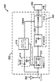
図8は、本発明の一例としての実施形態による、有線充電モジュール652およびワイヤレス充電受信器654を含む電子デバイス650の一部分のブロック図を例示する。必須ではないが、有線充電モジュール652は、PMIC内部にあってもよい。単に例として、有線充電モジュールは、図7に例示するPMIC510を備え得る。ワイヤレス充電受信器654は、本明細書では基準電圧と呼ぶ場合もある、内部バイアス電圧を発生させるように構成されるバイアス電圧発生器670を備え得る。ワイヤレス充電受信器654は、発生器670から内部バイアス電圧を受け取るように構成されるマルチプレクサ(MUX)664をさらに備え得る。MUX664は、リンク672を介して有線充電モジュール652からバイアス電圧(「WIRED_VTHERM_BIAS」)を受け取るようにさらに構成される。内部バイアス電圧およびWIRED_VTHERM_BIASの受け取りを基に、MUX664は、所望のバイアス電圧VTHERM_BIAS(すなわち、WIRED_VTHERM_BIASまたは内部バイアス電圧のいずれか)を、リンク658を介してサーミスタ675に伝達するように構成され得る。
FIG. 8 illustrates a block diagram of a portion of an
電子デバイス650は、バッテリユニット656をさらに含み得る、またはそれに結合され得る。例示のように、抵抗器R3は、バッテリユニット656の内部にあるサーミスタ675を備え、抵抗器R1およびR2は、各個がバッテリユニット656の外部にある。抵抗器R1、抵抗器R2、およびサーミスタR3は、分圧器661を編成する。本明細書で説明する一例としての実施形態はサーミスタを含むが、本発明の実施形態は、そのようには限定されないことに留意されたい。むしろ、バッテリユニット656は、温度を検知するための任意の適したセンサを備え得る、またはそれに結合され得る。分圧器661は、リンク660を介してMUX664にサーミスタ電圧VTHERM_INを出力するように構成される。
The
以下でより十分に説明するように、有線充電モジュール652がサーミスタ675にアクセス可能であるならば、MUX664は、リンク662を介して有線充電モジュール652にサーミスタ電圧VTHERM_INを伝達することができる。それに応答して、有線充電モジュール652は、バッテリユニット656の温度が容認可能な範囲内にあるかどうかを決定するために、VTHERM_INを様々なしきい値レベルと比較することができる。他方で、ワイヤレス充電受信器がサーミスタ675にアクセス可能であるならば、MUX664は、リンク663を介してモジュール674にサーミスタ電圧VTHERM_INを伝達することができる。モジュール674は、バッテリユニット656の温度が容認可能な範囲内にあるかどうかを決定するために、受け取ったサーミスタ電圧VTHERM_INを様々なしきい値レベルと比較するように構成される。モジュール674を、本明細書では「監視回路」と呼ぶ場合もあることに留意されたい。モジュール674を、デジタル比較器668に結合されるアナログデジタル変換器666を備えるように例示するが、本発明の実施形態は、そのようには限定されない。むしろ、モジュール674は、アナログ動作用に構成され得るものであり、図7に例示する比較器520のアレイと同様の、比較器のアレイを備え得る。
As described more fully below, if the
1つの一例としての実施形態によれば、以下でより十分に説明するように、MUX664は、VTHERM_BIASをサーミスタ675に、および、VTHERM_INをモジュール674または有線充電モジュール652のいずれかに提供するために、複数のスイッチを備え得る。別の一例としての実施形態によれば、MUX664は、VTHERM_BIASをサーミスタ675に、および、VTHERM_INをモジュール674または有線充電モジュール652のいずれかに提供するために、増幅器のアレイを備え得る。MUX664を、ワイヤレス充電受信器654内部にあるように例示するが、MUX664は、ワイヤレス充電受信器654の外部にあり、かつそれに動作可能に結合されてもよいということに留意されたい。
According to one exemplary embodiment,
次に、デバイス650の企図される動作を概略的に説明する。最初に、バイアス電圧発生器670により発生される内部バイアス電圧が、MUX664に提供され得る。電圧発生器670により発生される電圧は、MUX664に提供される前にスケーリングされ得ることに留意されたい。さらに、有線充電モジュール652により発生されるバイアス電圧WIRED_VTHERM_BIASが、MUX664にさらに提供され得る。2つのバイアス電圧を比較した後、MUX664は、より高い値を有するバイアス電圧をVTHERM_BIASとして、リンク658を介してサーミスタ675に伝達することができる。WIRED_VTHERM_BIASが、バイアス電圧発生器670により発生される内部バイアス電圧以上であるならば、有線充電モジュール652が、サーミスタ675にアクセス可能にされ得る(すなわち、WIRED_VTHERM_BIASが、サーミスタ675に伝達され、有線充電モジュール652が、バッテリユニット656の温度を検知する)ことに留意されたい。これを、「有線充電モード」と呼ぶ場合もある。WIRED_VTHERM_BIASが、バイアス電圧発生器670により発生される内部バイアス電圧未満であるならば、ワイヤレス充電受信器654が、サーミスタ675をバイアスするために直接アクセス可能にされ得る(すなわち、バイアス電圧発生器670により発生されるバイアス電圧が、サーミスタ675に伝達され、ワイヤレス充電受信器654が、バッテリユニット656の温度を検知する)。これを、「ワイヤレス充電モード」と呼ぶ場合もある。
Next, the intended operation of the
さらに、サーミスタ電圧VTHERM_INが、リンク660を介して抵抗分割器661からMUX664に提供され得る。有線充電モジュール652が、サーミスタ675にアクセス可能にされているならば、サーミスタ電圧VTHERM_INは、有線充電モジュール652に伝達され得るとともに、バッテリユニット656の温度が容認可能な範囲内にあるかどうかを決定するために、図7に示すように、比較器520のアレイを用いてしきい値電圧レベルと比較され得る。ワイヤレス充電受信器654が、サーミスタ675にアクセス可能にされているならば、サーミスタ電圧VTHERM_INは、バッテリユニット656の温度が容認可能な範囲内にあるかどうかを決定するために、サーミスタ電圧を様々なしきい値レベルと比較するために、モジュール674に伝達され得る。
In addition, the thermistor voltage VTHERM_IN may be provided from
図9は、本発明の一例としての実施形態による、有線充電モジュール652およびワイヤレス充電受信器654を含む電子デバイス700の一部分の回路図を例示する。有線充電モジュール652は、リンク708を介してバイアス電圧「WIRED_VTHERM_BIAS」を伝達するように、かつ、リンク710を介してサーミスタ電圧「VTHERM_IN」を受け取るように構成され得る。さらに、デバイス700は、サーミスタ675を備え得るバッテリユニット656を備え得る、またはそれに結合され得る。さらに、上記のように、本発明の実施形態は、サーミスタに限定されるのではなく、むしろ、温度を検知するための任意の適したセンサが、本発明の範囲内であり得る。デバイス700は、各個がバッテリユニット656の外部にある抵抗器R1、抵抗器R2、およびサーミスタ675を備える分圧器711をさらに含み得る。サーミスタ675を、バッテリユニット656の内部にあるように例示するが、サーミスタは、バッテリユニット656の外部および近傍にあってもよい。
FIG. 9 illustrates a circuit diagram of a portion of an
さらに、デバイス700は、最大電圧選択器706および調整器704(例えば、LDO)を含み得る。調整器704は、最大電圧選択器706に内部バイアス電圧(「内部バイアス電圧」)を供給するように構成され得る。したがって、最大電圧選択器706は、リンク708を介して、有線充電モジュール652からバイアス電圧WIRED_VTHERM_BIASを受け取るように、かつ、リンク709を介して、調整器704から内部バイアス電圧を受け取るように構成され得る。バイアス電圧を受け取ると、最大電圧選択器706は、ワイヤレス充電受信器654と有線充電モジュール652との間の優先順位を定義するように構成され得る。より具体的には、最大電圧選択器706によって、バイアス電圧VTHERM_BIASが、リンク719を介してサーミスタ675に伝達されることが可能になり得る。バイアス電圧VTHERM_BIASは、バイアス電圧WIRED_VTHERM_BIASまたは内部バイアス電圧の大きな方を含むことに留意されたい。さらになお具体的には、バイアス電圧WIRED_VTHERM_BIASが内部バイアス電圧以上であるならば、有線充電モジュール652が、サーミスタ675にアクセス可能にされ得る(すなわち、バイアス電圧WIRED_VTHERM_BIASがサーミスタ675に伝達される)。さらに、バイアス電圧WIRED_VTHERM_BIASが内部バイアス電圧以上であるならば、分圧器711から出力されるサーミスタ電圧VTHERM_INが、リンク722および710を介して有線充電モジュールに伝達され得る。さらに、バイアス電圧WIRED_VTHERM_BIASが内部バイアス電圧未満であるならば、ワイヤレス充電受信器654が、サーミスタ675をバイアスするために直接アクセス可能にされ得る(すなわち、内部バイアス電圧がサーミスタ675に伝達される)。さらに、バイアス電圧WIRED_VTHERM_BIASが内部バイアス電圧未満であるならば、分圧器711から出力されるサーミスタ電圧VTHERM_INが、リンク723を介してモジュール674に伝達され得る。
Further, the
上記のように、ワイヤレス充電受信器654、および、より具体的には、MUX664(図8を参照)は、所望のバイアス電圧をサーミスタ675に提供するために、複数のスイッチを含み得る。より具体的には、ワイヤレス充電受信器654は、スイッチS1、S2、S3、S4、S5、およびS6を備え得る。図8のMUX664内部に含まれ得るスイッチS1、S2、S3、およびS4は、有線充電モジュール652と、調整器704と、モジュール674との間の接続を提供し得る。スイッチS5およびS6は、以下で説明する。スイッチS1〜S4を備え得る図8のMUX664、および最大電圧選択器706を、本明細書では、合わせて「インターフェース」と呼ぶ場合があることに留意されたい。
As described above, the
デバイス700は、上記のように、バッテリユニット656の温度が容認可能な範囲内にあるかどうかを決定するために、サーミスタ電圧VTHERM_INを様々なしきい値レベルと比較するように構成され得る、モジュール674をさらに含む。図9に例示する実施形態では、モジュール674は、プログラマブル基準スイッチS5およびS6を伴うNビットアナログデジタル変換器666、低オフセットのバッファ714、ならびにマイクロコントローラ668を備える。単に例として、Nビットアナログデジタル変換器666は、8ビットアナログデジタル変換器を備え得る。
スイッチS5およびS6によって、アナログデジタル変換器666用の基準電圧が、プログラマブルであることが可能になり得る。より具体的には、マイクロコントローラ668は、バッファ714から出力される、バッファリングされたサーミスタ電圧VTHERM_IN_BUFに、アナログデジタル変換器666のフルスケールレンジを整合させるために、サーミスタのチャネルのアナログデジタル変換器666の要求の間、スイッチS5をターン「オン」する(すなわち、バイアス電圧VTHERM_BIASが、アナログデジタル変換器666用に使用される)ように構成され得る。これによって、アナログデジタル変換器666用の最小分解能を用いた、向上した精度のサーミスタ電圧測定のために、アナログデジタル変換器666の分解能が最大になり得る。すべての他のチャネルの変換要求に対して、マイクロコントローラ668は、アナログデジタル変換器666用に内部基準電圧Vrefを使用するために、スイッチS5をターン「オフ」し、スイッチS6をターン「オン」することができる。
Switches S5 and S6 may allow the reference voltage for analog to
バッテリユニット656の温度は、マイクロコントローラ668からのアナログデジタル変換器の変換要求によってサンプリングされ、既定のしきい値と比較される。次いで、マイクロコントローラ668は、バッテリユニット656の温度が充電に関して安全な枠内にあることを検証するために、比較の結果を使用することができる。バッファ714は、アナログデジタル変換器666の入力インピーダンスを外部サーミスタの抵抗分割器711から分離するように構成され得ることに留意されたい。これは、より高速な変換時間を可能にし得るとともに、アナログデジタル変換器の入力インピーダンスが変換中に変化させる入力に起因する、精度の損失を防止することができる。
The temperature of the
次に、デバイス700の企図される動作を説明する。最初に、調整器704から発生される内部バイアス電圧が、抵抗器673および671を備える抵抗分割器によりスケーリングされ得る。次いで、スケーリングされたバイアス電圧(「内部バイアス電圧」)が、比較器677ならびにスイッチ679および681を備え得る、最大電圧選択器706の入力に提供され得る。単に例として、内部バイアス電圧は、20%だけスケーリングされ得る。別の言い方をすれば、最大電圧選択器706に提供されるスケーリングされたバイアス電圧は、調整器704により発生される電圧の80%であり得る。さらに、有線充電モジュール652からのバイアス電圧(「WIRED_VTHERM_BIAS」)が、リンク708を介して最大電圧選択器706の入力にさらに伝達され得る。その後、内部バイアス電圧およびバイアス電圧WIRED_VTHERM_BIASは、最大電圧選択器706により比較され得る。調整器704により発生されるバイアス電圧をスケーリングすることが、バイアス電圧WIRED_VTHERM_BIASが内部バイアス電圧に等しいという状況を防止し得るということに留意されたい。これは、最大電圧選択器706によって、発振および/または高いリーク電流という望ましくない結果をもたらす場合がある。
The intended operation of
最大電圧選択器706は、バイアス電圧WIRED_VTHERM_BIASが内部バイアス電圧以上であるとき、スイッチS2を開状態にし、スイッチS1、S3、およびS4を閉状態にするように構成され得る。したがって、バイアス電圧WIRED_VTHERM_BIASが内部バイアス電圧以上であるとき、有線充電モジュール652が、サーミスタ675をバイアスするために直接アクセス可能にされる。別の言い方をすれば、有線充電モジュールは、サーミスタ675をバイアスし、バッテリユニット656の温度を検知することができる。
さらに、最大電圧選択器706は、バイアス電圧WIRED_VTHERM_BIASが内部バイアス電圧未満であるとき、スイッチS2を閉状態にし、スイッチS1、S3、およびS4を開状態にするように構成され得る。したがって、バイアス電圧WIRED_VTHERM_BIASが内部バイアス電圧未満であるとき、ワイヤレス充電受信器654が、サーミスタ675をバイアスするために直接アクセス可能にされる。別の言い方をすれば、ワイヤレス充電受信器654は、サーミスタ675をバイアスし、バッテリユニット656の温度を検知することができる。
Further,
上記のように、マイクロコントローラ668は、バッファ714から出力される、バッファリングされたサーミスタ電圧VTHERM_IN_BUFに、アナログデジタル変換器666のフルスケールレンジを整合させるために、サーミスタのチャネルのアナログデジタル変換器の要求の間、スイッチS5をターン「オン」するように構成され得る。すべての他のチャネルの変換要求に対して、マイクロコントローラ668は、アナログデジタル変換器666用に内部基準電圧Vrefを使用するために、スイッチS5をターン「オフ」し、スイッチS6をターン「オン」することができる。
As described above, the
最大電圧選択器706の出力である電圧Vmax_outは、インバータ720、およびスイッチS1〜S4のバルク接続に対する供給として使用され得ることに留意されたい。したがって、ワイヤレス充電受信器654は、関連する充電可能デバイスが、充電パッド上になく、有線充電バイアス電圧以外の入力供給がないときでさえ、機能的であり得る。有線充電モジュール652および有線充電バイアス電圧が存在しない例では、最大電圧選択器706が、スイッチS2を閉状態にし、スイッチS1、S3、およびS4を開状態にすることができる。内部バイアス電圧は、調整器704からサーミスタ675をバイアスし、リンク722からリンク710を切断する。
Note that the voltage Vmax_out, which is the output of the
図10は、ワイヤレス充電受信器(例えば、ワイヤレス充電受信器654)がオンであり、有線充電モジュール(例えば、有線充電モジュール652)が、オンの位置とオフの位置との間でトグルするユースケースのシーケンスに関する、デバイス700の様々な電流および電圧のレベルを例示するタイミング図900を例示する。タイミング図900は、インターフェース(すなわち、MUX664および最大電圧選択器706)の自動的な優先順位の指定を例示する。タイミング図900は、ワイヤレス充電受信器(例えば、ワイヤレス充電受信器654)がオンであり、有線充電モジュール(例えば、有線充電モジュール652)が、オンの位置とオフの位置との間でトグルする動作を図示することに留意されたい。次に、図9および10を参照して、タイミング図900を説明する。信号902は、内部バイアス電圧の電圧レベルを表し、信号904は、有線充電バイアス電圧(「WIRED_VTHERM_BIAS」)の電圧レベルを表す。さらに、信号906は、電圧Vmax_outの電圧レベルを表す。信号908は、サーミスタ675に伝達されるバイアス電圧(「VTHERM_BIAS」)の電圧レベルを表す。
FIG. 10 shows a use case where a wireless charging receiver (e.g., wireless charging receiver 654) is on and a wired charging module (e.g., wired charging module 652) toggles between an on position and an off position. 6 illustrates a timing diagram 900 illustrating various current and voltage levels of the
信号912は、リンク710を介して有線充電モジュール652に伝達されるサーミスタ電圧(「VTHERM_IN」)の電圧レベルを表し、信号910は、バッファ714から出力される電圧レベル(「VTHERM_IN_BUF」)を表す。さらに、信号914は、調整器704から最大電圧選択器706に供給される電流レベルを表し、信号916は、有線充電モジュール652から最大電圧選択器706に供給される電流レベルを表す。有線充電モジュール652がオンであり、有線充電バイアス電圧(すなわち、信号904)が1.8ボルトであるとき、Vmax_out(すなわち、信号906)もまた1.8Vであることに留意されたい。有線充電バイアス電圧(すなわち、信号904)が、ターンオンし、内部バイアス電圧(すなわち、信号902)より高くなる(すなわち、2.2V>1.8V)と、Vmax_out(すなわち、信号906)およびVTHERM_BIAS(すなわち、信号908)が、2.2Vでの有線充電バイアス電圧に接続される。次いで、有線充電バイアス電圧(すなわち、信号904)がターンオフされる。次いで、Vmax_out(すなわち、信号906)およびVTHERM_BIAS(908)が、1.8Vでの有線充電バイアス電圧(すなわち、信号904)に低下する。
The
図11は、有線充電モジュール(例えば、有線充電モジュール652)がオンであり、ワイヤレス充電受信器(例えば、ワイヤレス充電受信器654)が、オンとオフとの間の立場でトグルするユースケースのシーケンスに関する、デバイス700の様々な電流および電圧のレベルを例示するタイミング図940を例示する。タイミング図940は、インターフェース(すなわち、MUX664および最大電圧選択器706)の自動的な優先順位の指定を例示する。次に、図9および11を参照して、タイミング図940を説明する。信号952は、内部バイアス電圧の電圧レベルを表し、信号950は、有線充電バイアス電圧(「WIRED_VTHERM_BIAS」)の電圧レベルを表す。さらに、信号954は、電圧Vmax_outの電圧レベルを表す。信号956は、サーミスタ675に伝達されるバイアス電圧(「VTHERM_BIAS」)の電圧レベルを表す。信号958は、リンク710を介して有線充電モジュール652に伝達されるサーミスタ電圧(「VTHERM_IN」)の電圧レベルを表し、信号960は、バッファ714から出力される電圧レベル(「VTHERM_IN_BUF」)を表す。さらに、信号962は、調整器704から最大電圧選択器706に供給される電流レベルを表し、信号964は、有線充電モジュール652から最大電圧選択器706に供給される電流レベルを表す。有線充電バイアス電圧(すなわち、信号950)が、1.8Vでの内部バイアス電圧(すなわち、信号952)より高い2.2Vであることに留意されたい。したがって、Vmax_out(すなわち、信号954)およびVTHERM_BIAS(すなわち、信号956)は変化しない。デバイス700は、ワイヤレス充電受信器654がターンオンおよびターンオフされるにもかかわらず、有線充電モード用に構成されたままである。
FIG. 11 shows a sequence of use cases where a wired charging module (e.g., wired charging module 652) is on and a wireless charging receiver (e.g., wireless charging receiver 654) toggles between on and off. FIG. 9 illustrates a timing diagram 940 illustrating various current and voltage levels of the
図12は、1つまたは複数の一例としての実施形態による方法990を例示するフローチャートである。方法990は、インターフェースを介して、ワイヤレス電力受信器をバッテリユニットに結合するステップを含み得る(数表示992により図示する)。さらに、方法990は、インターフェースを介して、有線充電モジュールをバッテリユニットに結合するステップを含み得る(数表示994により図示する)。方法990は、インターフェースを介して、ワイヤレス電力受信器および有線充電モジュールの1つが、バッテリユニットの温度を決定する(determine)ことを選択的に可能にするステップをさらに含み得る(数表示996により図示する)。
FIG. 12 is a flowchart illustrating a
情報および信号を、任意の種々の異なる技術および技法を使用して表すことができることを、当業者は理解するであろう。例えば、上記の説明の全体を通して参照され得るデータ、命令、コマンド、情報、信号、ビット、記号、およびチップを、電圧、電流、電磁波、磁気的な場もしくは粒子、光学的な場もしくは粒子、またはそれらの任意の組み合わせにより表すことができる。 Those of skill in the art will understand that information and signals may be represented using any of a variety of different technologies and techniques. For example, data, instructions, commands, information, signals, bits, symbols, and chips that can be referred to throughout the above description, voltage, current, electromagnetic wave, magnetic field or particle, optical field or particle, or It can be represented by any combination thereof.
本明細書で開示した一例としての実施形態に連関して説明した、様々な例示的な論理ブロック、モジュール、回路、およびアルゴリズムステップを、電子ハードウェア、コンピュータソフトウェア、またはその両方の組み合わせとして実装可能であることを、当業者はさらに理解するであろう。ハードウェアおよびソフトウェアのこの互換性を明確に例示するために、様々な例示的な構成要素、ブロック、モジュール、回路、およびステップを、それらの機能性に関して概略的に上記で説明した。そのような機能性をハードウェアとして実装するか、それともソフトウェアとして実装するかは、個々の用途、およびシステム全体に課せられた設計制約によって決まる。当業者であれば、各個の個々の用途に対して様々な方法で、説明した機能性を実装することができるが、そのような実装形態の決定を、本発明の一例としての実施形態の範囲からの逸脱をもたらすものと解釈すべきではない。 Various exemplary logic blocks, modules, circuits, and algorithm steps described in connection with the example embodiments disclosed herein can be implemented as electronic hardware, computer software, or a combination of both. Those skilled in the art will further understand that. To clearly illustrate this interchangeability of hardware and software, various illustrative components, blocks, modules, circuits, and steps have been described above generally in terms of their functionality. Whether such functionality is implemented as hardware or software depends on the particular application and design constraints imposed on the overall system. Those skilled in the art can implement the described functionality in a variety of ways for each individual application, but such implementation decisions are within the scope of the exemplary embodiments of the present invention. Should not be construed as causing deviations from
本明細書で開示した一例としての実施形態に連関して説明した、様々な例示的な論理ブロック、モジュール、および回路を、本明細書で説明した機能を遂行するように設計された、汎用プロセッサ、デジタル信号プロセッサ(DSP)、特定用途向け集積回路(ASIC)、フィールドプログラマブルゲートアレイ(FPGA)もしくは他のプログラマブル論理デバイス、個別的なゲートもしくはトランジスタ論理回路、個別的なハードウェア構成要素、またはそれらの任意の組み合わせを用いて、実装または遂行することができる。汎用プロセッサは、マイクロプロセッサであってよいが、代替として、プロセッサは、任意の従来のプロセッサ、コントローラ、マイクロコントローラ、または状態機械であってよい。プロセッサを、コンピューティングデバイスの組み合わせ、例えば、DSPとマイクロプロセッサとの組み合わせ、複数のマイクロプロセッサ、DSPコアと連動した1つもしくは複数のマイクロプロセッサ、または任意の他のそのような構成として実装することもできる。 A general purpose processor designed to perform the functions described herein with the various exemplary logic blocks, modules, and circuits described in connection with the example embodiments disclosed herein. Digital signal processor (DSP), application specific integrated circuit (ASIC), field programmable gate array (FPGA) or other programmable logic device, individual gate or transistor logic, individual hardware components, or Any combination of can be implemented or performed. A general purpose processor may be a microprocessor, but in the alternative, the processor may be any conventional processor, controller, microcontroller, or state machine. Implementing the processor as a combination of computing devices, eg, a combination of DSP and microprocessor, multiple microprocessors, one or more microprocessors in conjunction with a DSP core, or any other such configuration You can also.
本明細書で開示した一例としての実施形態に連関して説明した方法またはアルゴリズムのステップを、ハードウェアで、プロセッサにより実行されるソフトウェアモジュールで、またはその2つの組み合わせで直接実施することができる。ソフトウェアモジュールは、ランダムアクセスメモリ(RAM)、フラッシュメモリ、リードオンリーメモリ(ROM)、電気的プログラマブルROM(EPROM)、電気的消去可能プログラマブルROM(EEPROM)、レジスタ、ハードディスク、リムーバブルディスク、CD-ROM、または当技術分野で知られている任意の他の形態の記憶媒体に存在し得る。一例としての記憶媒体は、プロセッサが、記憶媒体から情報を読み出すことができ、かつ、記憶媒体に情報を書き込むことができるように、プロセッサに結合される。代替として、記憶媒体は、プロセッサと一体であり得る。プロセッサおよび記憶媒体は、ASICに存在し得る。ASICは、ユーザ端末に存在し得る。代替として、プロセッサおよび記憶媒体は、ユーザ端末に個別的な構成要素として存在し得る。 The method or algorithm steps described in connection with the example embodiments disclosed herein may be implemented directly in hardware, in software modules executed by a processor, or in a combination of the two. Software modules include random access memory (RAM), flash memory, read only memory (ROM), electrically programmable ROM (EPROM), electrically erasable programmable ROM (EEPROM), register, hard disk, removable disk, CD-ROM, Or it may reside in any other form of storage medium known in the art. An exemplary storage medium is coupled to the processor such that the processor can read information from, and write information to, the storage medium. In the alternative, the storage medium may be integral to the processor. The processor and the storage medium can reside in an ASIC. The ASIC may be present in the user terminal. In the alternative, the processor and the storage medium may reside as discrete components in a user terminal.
1つまたは複数の一例としての実施形態では、説明した機能を、ハードウェア、ソフトウェア、ファームウェア、またはそれらの任意の組み合わせで実装することができる。ソフトウェアで実装するならば、機能を、コンピュータ可読媒体上の1つまたは複数の、命令またはコードとして、コンピュータ可読媒体に記憶すること、またはそれを介して送信することができる。コンピュータ可読媒体は、1つの場所から別の場所へのコンピュータプログラムの移送を容易にする任意の媒体を含む、コンピュータ記憶媒体と通信媒体の両方を含む。記憶媒体は、コンピュータによりアクセスされ得る任意の利用可能な媒体であり得る。例として、かつ限定ではなく、そのようなコンピュータ可読媒体は、RAM、ROM、EEPROM、CD-ROMもしくは他の光ディスク記憶装置、磁気ディスク記憶装置もしくは他の磁気記憶デバイス、または、所望のプログラムコードを命令もしくはデータ構造の形態で、搬送もしくは記憶するために使用され得る、かつ、コンピュータによりアクセスされ得る、任意の他の媒体を含み得る。さらに、当然のことながら、任意の接続をコンピュータ可読媒体と呼ぶ。例えば、ソフトウェアを、同軸ケーブル、光ファイバケーブル、ツイストペア、デジタル加入者線(DSL)、または、赤外線、無線、およびマイクロ波などのワイヤレス技術を使用して、ウェブサイト、サーバ、または他のリモートソースから送信するならば、同軸ケーブル、光ファイバケーブル、ツイストペア、DSL、または、赤外線、無線、およびマイクロ波などのワイヤレス技術は、媒体の定義に含まれる。本明細書で使用される際、ディスク(disk)およびディスク(disc)とは、コンパクトディスク(compact disc)(CD)、レーザディスク(laser disc)、光ディスク(optical disc)、デジタルバーサタイルディスク(digital versatile disc)(DVD)、フロッピー(登録商標)ディスク(floppy disk)、およびブルーレイディスク(blu-ray disc)を含み、diskは、通常はデータを磁気的に再生し、一方でdiscは、レーザを用いてデータを光学的に再生する。上記の組み合わせもまた、コンピュータ可読媒体の範囲内に含まれるべきである。 In one or more example embodiments, the functions described may be implemented in hardware, software, firmware, or any combination thereof. If implemented in software, the functions may be stored on or transmitted over as one or more instructions or code on a computer-readable medium. Computer-readable media includes both computer storage media and communication media including any medium that facilitates transfer of a computer program from one place to another. A storage media may be any available media that can be accessed by a computer. By way of example and not limitation, such computer readable media may be RAM, ROM, EEPROM, CD-ROM or other optical disk storage, magnetic disk storage or other magnetic storage device, or desired program code. It may include any other medium that can be used for carrying or storing in the form of instructions or data structures and that can be accessed by a computer. Furthermore, it will be appreciated that any connection is referred to as a computer readable medium. For example, software, websites, servers, or other remote sources using coaxial cable, fiber optic cable, twisted pair, digital subscriber line (DSL), or wireless technologies such as infrared, wireless, and microwave If transmitting from a coaxial cable, fiber optic cable, twisted pair, DSL, or wireless technologies such as infrared, radio, and microwave are included in the definition of the medium. As used herein, a disk and a disc are a compact disc (CD), a laser disc, an optical disc, a digital versatile disc (digital versatile disc). disc) (DVD), floppy disk, and blu-ray disc, the disk normally reproducing data magnetically, while the disc uses a laser To optically reproduce the data. Combinations of the above should also be included within the scope of computer-readable media.
開示した一例としての実施形態の先の説明は、当業者ならば誰でも、本発明を作製または使用することを可能にするために提供される。これらの一例としての実施形態に対する様々な修正は、当業者に容易に明らかになるものであり、本明細書で定義する一般的な原理は、本発明の趣旨または範囲から逸脱することなく、他の実施形態に適用され得る。したがって、本発明は、本明細書で示した一例としての実施形態に限定されることが意図されるのではなく、本明細書で開示した原理および新規の特徴と合致する最大限の範囲が与えられるべきである。 The previous description of the disclosed exemplary embodiments is provided to enable any person skilled in the art to make or use the present invention. Various modifications to these example embodiments will be readily apparent to those skilled in the art, and the general principles defined herein may be used without departing from the spirit or scope of the invention. This embodiment can be applied. Accordingly, the present invention is not intended to be limited to the exemplary embodiments shown herein but is to be accorded the widest scope consistent with the principles and novel features disclosed herein. Should be done.
100 ワイヤレス送信または充電システム
102 入力電力
104 送信器
106 放射場
108 受信器
110 出力電力
112 距離
114 送信アンテナ
118 受信アンテナ
119 通信チャネル
122 発振器
123 調整信号
124 電力増幅器
125 制御信号
126 フィルタおよび整合回路
132 整合回路
134 整流器およびスイッチング回路
136 バッテリ
150 ループアンテナ
152、154 コンデンサ
156 共振信号
200 送信器
202 送信回路網
204 送信アンテナ
206 固定インピーダンス整合回路
208 ローパスフィルタ(LPF)
210 電力増幅器
212 発振器
214 コントローラ
216 負荷検知回路
280 存在検出器
260 密閉検出器
300 受信器
302 受信回路網
304 受信アンテナ
306 電力変換回路網
308 RF-DC変換器
310 DC-DC変換器
312 スイッチング回路網
314 シグナリング検出器およびビーコン回路網
316 プロセッサ
350 デバイス
500 プロット
502 信号
510 電力管理集積回路、PMIC
512 バッテリ
514 抵抗分割器
518 サーミスタ
520 比較器
540 最大電圧選択器
650 電子デバイス
652 有線充電モジュール
654 ワイヤレス充電受信器
656 バッテリユニット
658、660 リンク
661 分圧器、抵抗分割器
662、663 リンク
664 マルチプレクサ、MUX
666 アナログデジタル変換器
668 デジタル比較器、マイクロコントローラ
670 バイアス電圧発生器
671 抵抗器
672 リンク
673 抵抗器
674 モジュール
675 サーミスタ
677 比較器
679、681 スイッチ
700 電子デバイス
704 調整器
706 最大電圧選択器
708、709、710 リンク
711 分圧器、抵抗分割器
714 バッファ
719 リンク
720 インバータ
722、723 リンク
900 タイミング図
902、904、906、908、910、912、914、916 信号
940 タイミング図
950、952、954、956、958、960、962、964 信号
990 方法
992、994、996 数表示
100 wireless transmission or charging system
102 Input power
104 transmitter
106 Radiation field
108 Receiver
110 Output power
112 distance
114 Transmit antenna
118 Receive antenna
119 communication channel
122 oscillator
123 Adjustment signal
124 Power amplifier
125 Control signal
126 Filters and matching circuits
132 Matching circuit
134 Rectifiers and switching circuits
136 battery
150 loop antenna
152, 154 capacitors
156 Resonant signal
200 transmitter
202 Transmitter network
204 Transmit antenna
206 Fixed impedance matching circuit
208 Low pass filter (LPF)
210 Power amplifier
212 oscillator
214 controller
216 Load detection circuit
280 Presence detector
260 Sealed detector
300 receiver
302 Receiver network
304 receiving antenna
306 Power conversion network
308 RF-DC converter
310 DC-DC converter
312 Switching network
314 Signaling Detector and Beacon Network
316 processor
350 devices
500 plots
502 signal
510 Power management integrated circuit, PMIC
512 battery
514 resistor divider
518 Thermistor
520 comparator
540 Maximum voltage selector
650 electronic devices
652 Wired charging module
654 wireless charging receiver
656 Battery unit
658, 660 links
661 voltage divider, resistor divider
662, 663 links
664 Multiplexer, MUX
666 analog to digital converter
668 Digital comparator, microcontroller
670 Bias voltage generator
671 resistors
672 links
673 resistors
674 modules
675 thermistor
677 comparator
679, 681 switch
700 electronic devices
704 Regulator
706 Maximum voltage selector
708, 709, 710 links
711 voltage divider, resistor divider
714 buffer
719 links
720 inverter
722, 723 links
900 Timing diagram
902, 904, 906, 908, 910, 912, 914, 916 signals
940 Timing diagram
950, 952, 954, 956, 958, 960, 962, 964 signals
990 method
992, 994, 996 number display
Claims (26)
前記ワイヤレス電力受信器に動作可能に結合される有線充電モジュールと、
バッテリユニットに結合するように、かつ、前記ワイヤレス電力受信器および前記有線充電モジュールの1つが、前記バッテリユニットの温度を測定することを選択的に可能にするように構成されているインターフェースと、
を備えることを特徴とするデバイス。 A wireless power receiver;
A wired charging module operably coupled to the wireless power receiver;
An interface coupled to a battery unit and configured to selectively allow one of the wireless power receiver and the wired charging module to measure the temperature of the battery unit;
A device comprising:
前記インターフェースを介して、有線充電モジュールを前記バッテリユニットに結合するステップと、
前記ワイヤレス電力受信器および前記有線充電モジュールの1つを、前記インターフェースを介して、前記バッテリユニットの温度を測定することを選択的に可能にするステップと、
を含むことを特徴とする方法。 Coupling the wireless power receiver to the battery unit via the interface;
Coupling a wired charging module to the battery unit via the interface;
Selectively enabling one of the wireless power receiver and the wired charging module to measure the temperature of the battery unit via the interface;
A method comprising the steps of:
前記バイアス電圧が前記別のバイアス電圧以上であるならば、バッテリユニットに電力を伝達する前に、センサをバイアスし、前記バッテリユニットの前記温度を検知する前記有線充電モジュールを選択するステップと、
前記バイアス電圧が前記別のバイアス電圧未満であるならば、前記バッテリユニットに電力を伝達する前に、前記バッテリユニットの前記温度を検知する前記ワイヤレス電力受信器を選択するステップと、
をさらに含むことを特徴とする請求項13に記載の方法。 Comparing a bias voltage generated by the wired charging module with another bias voltage generated by the wireless power receiver;
Selecting the wired charging module to bias a sensor and sense the temperature of the battery unit prior to transferring power to the battery unit if the bias voltage is greater than or equal to the other bias voltage;
Selecting the wireless power receiver to sense the temperature of the battery unit before transferring power to the battery unit if the bias voltage is less than the other bias voltage;
14. The method of claim 13, further comprising:
前記インターフェースを介して、有線充電モジュールを前記バッテリユニットに結合するための手段と、
前記インターフェースを介して、前記ワイヤレス電力受信器および前記有線充電モジュールの1つに、前記バッテリユニットの温度を測定することを選択的に可能にするための手段と、
を備えることを特徴とするデバイス。 Means for coupling the wireless power receiver to the battery unit via the interface;
Means for coupling a wired charging module to the battery unit via the interface;
Means for selectively enabling one of the wireless power receiver and one of the wired charging modules to measure the temperature of the battery unit via the interface;
A device comprising:
前記インターフェースを介して、有線充電モジュールを前記バッテリユニットに結合するための前記手段が、前記有線充電モジュールと前記バッテリユニットとの間で信号を送受信するための回路を備え、
前記インターフェースを介して、前記ワイヤレス電力受信器および前記有線充電モジュールの1つに、前記バッテリユニットの温度を測定することを選択的に可能にするための手段が、前記インターフェースを介して、前記ワイヤレス電力受信器および前記有線充電モジュールの1つが、前記バッテリユニットの温度を測定することを選択的に可能にするために、複数のスイッチを備えるマルチプレクサを備える回路を備えることを特徴とする請求項22に記載のデバイス。 The means for coupling a wireless power receiver to a battery unit via an interface comprises a circuit for transmitting and receiving signals between the wireless power receiver and the battery unit;
The means for coupling a wired charging module to the battery unit via the interface comprises a circuit for transmitting and receiving signals between the wired charging module and the battery unit;
Means for selectively enabling the wireless power receiver and one of the wired charging modules via the interface to measure the temperature of the battery unit via the interface 23. One of the power receiver and the wired charging module comprises a circuit comprising a multiplexer with a plurality of switches to selectively enable the temperature of the battery unit to be measured. Device described in.
Applications Claiming Priority (5)
| Application Number | Priority Date | Filing Date | Title |
|---|---|---|---|
| US34973410P | 2010-05-28 | 2010-05-28 | |
| US61/349,734 | 2010-05-28 | ||
| US12/959,253 US8704484B2 (en) | 2010-05-28 | 2010-12-02 | Temperature sensor interface for wireless and wired charging |
| US12/959,253 | 2010-12-02 | ||
| PCT/US2011/038252 WO2011150287A2 (en) | 2010-05-28 | 2011-05-26 | Temperature sensor interface for wireless and wired charging |
Publications (2)
| Publication Number | Publication Date |
|---|---|
| JP2013533720A true JP2013533720A (en) | 2013-08-22 |
| JP5619993B2 JP5619993B2 (en) | 2014-11-05 |
Family
ID=44627687
Family Applications (1)
| Application Number | Title | Priority Date | Filing Date |
|---|---|---|---|
| JP2013512263A Expired - Fee Related JP5619993B2 (en) | 2010-05-28 | 2011-05-26 | Temperature sensor interface for wireless and wired charging |
Country Status (6)
| Country | Link |
|---|---|
| US (1) | US8704484B2 (en) |
| EP (1) | EP2577841A2 (en) |
| JP (1) | JP5619993B2 (en) |
| KR (1) | KR101823172B1 (en) |
| CN (1) | CN102918741B (en) |
| WO (1) | WO2011150287A2 (en) |
Cited By (1)
| Publication number | Priority date | Publication date | Assignee | Title |
|---|---|---|---|---|
| KR20160028352A (en) * | 2014-08-19 | 2016-03-11 | 한국전자통신연구원 | Wire and wireless storage apparatus |
Families Citing this family (50)
| Publication number | Priority date | Publication date | Assignee | Title |
|---|---|---|---|---|
| US8202248B2 (en) | 2004-08-18 | 2012-06-19 | Sequana Medical Ag | Dialysis implant and methods of use |
| US9391461B2 (en) * | 2011-05-31 | 2016-07-12 | Samsung Electronics Co., Ltd. | Wireless power transmission and charging system, and power control method of wireless power transmission and charging system |
| JP6032900B2 (en) | 2012-02-06 | 2016-11-30 | キヤノン株式会社 | Electronics |
| US8585635B2 (en) | 2012-02-15 | 2013-11-19 | Sequana Medical Ag | Systems and methods for treating chronic liver failure based on peritoneal dialysis |
| KR101920236B1 (en) * | 2012-06-19 | 2018-11-20 | 삼성전자주식회사 | Method for charging battery and an electronic device thereof |
| KR102158288B1 (en) * | 2012-07-09 | 2020-09-21 | 삼성전자주식회사 | Method for charging battery and an electronic device thereof |
| WO2014018971A1 (en) | 2012-07-27 | 2014-01-30 | Thoratec Corporation | Resonant power transfer systems with protective algorithm |
| US10291067B2 (en) | 2012-07-27 | 2019-05-14 | Tc1 Llc | Computer modeling for resonant power transfer systems |
| WO2014018969A2 (en) | 2012-07-27 | 2014-01-30 | Thoratec Corporation | Resonant power transfer system and method of estimating system state |
| EP2878060A4 (en) * | 2012-07-27 | 2016-04-06 | Thoratec Corp | Wireless battery charging |
| EP4257174A3 (en) | 2012-07-27 | 2023-12-27 | Tc1 Llc | Thermal management for implantable wireless power transfer systems |
| US9287040B2 (en) | 2012-07-27 | 2016-03-15 | Thoratec Corporation | Self-tuning resonant power transfer systems |
| WO2014018974A1 (en) | 2012-07-27 | 2014-01-30 | Thoratec Corporation | Magnetic power transmission utilizing phased transmitter coil arrays and phased receiver coil arrays |
| WO2014018973A1 (en) | 2012-07-27 | 2014-01-30 | Thoratec Corporation | Resonant power transmission coils and systems |
| US10383990B2 (en) | 2012-07-27 | 2019-08-20 | Tc1 Llc | Variable capacitor for resonant power transfer systems |
| US9529055B2 (en) * | 2012-10-09 | 2016-12-27 | Nissan Motor Co., Ltd. | Impedance measuring device for laminated battery |
| US9455596B2 (en) | 2012-10-16 | 2016-09-27 | Ford Global Technologies, Llc | System and method for reducing interference between wireless charging and amplitude modulation reception |
| US9124124B2 (en) | 2012-10-16 | 2015-09-01 | Ford Global Technologies, Llc | System and method for reducing interference during wireless charging |
| US9065157B2 (en) * | 2012-11-08 | 2015-06-23 | Ford Global Technologies, Llc | System and method for reducing thermal conditions during wireless charging |
| US9637016B2 (en) * | 2012-12-14 | 2017-05-02 | Agim GJINALI | Fast charging system for electric vehicles |
| US9148033B2 (en) | 2012-12-21 | 2015-09-29 | Ford Global Technologies, Llc | System of securing a wide-range of devices during wireless charging |
| US9472963B2 (en) | 2013-02-06 | 2016-10-18 | Ford Global Technologies, Llc | Device for wireless charging having a plurality of wireless charging protocols |
| US9577459B2 (en) * | 2013-03-15 | 2017-02-21 | Sequana Medical Ag | Systems and methods for regulating inductive energy transfer to an implantable system |
| WO2014145664A1 (en) | 2013-03-15 | 2014-09-18 | Thoratec Corporation | Integrated implantable tets housing including fins and coil loops |
| WO2014145895A1 (en) | 2013-03-15 | 2014-09-18 | Thoratec Corporation | Malleable tets coil with improved anatomical fit |
| US9381821B2 (en) | 2013-05-15 | 2016-07-05 | Qualcomm Incorporated | Systems, methods, and apparatus related to electric vehicle wired and wireless charging |
| US9401622B2 (en) * | 2013-07-23 | 2016-07-26 | Qualcomm Incorporated | Systems and methods for extending the power capability of a wireless charger |
| US9490653B2 (en) * | 2013-07-23 | 2016-11-08 | Qualcomm Incorporated | Systems and methods for enabling a universal back-cover wireless charging solution |
| US10615642B2 (en) | 2013-11-11 | 2020-04-07 | Tc1 Llc | Resonant power transfer systems with communications |
| EP3069358B1 (en) | 2013-11-11 | 2019-06-12 | Tc1 Llc | Hinged resonant power transfer coil |
| EP3072211A4 (en) | 2013-11-11 | 2017-07-05 | Thoratec Corporation | Resonant power transfer systems with communications |
| CN104753034B (en) * | 2013-12-27 | 2018-10-12 | 富泰华工业(深圳)有限公司 | Electronic device and its charge protector |
| US10610692B2 (en) | 2014-03-06 | 2020-04-07 | Tc1 Llc | Electrical connectors for implantable devices |
| US10186760B2 (en) | 2014-09-22 | 2019-01-22 | Tc1 Llc | Antenna designs for communication between a wirelessly powered implant to an external device outside the body |
| US9583874B2 (en) | 2014-10-06 | 2017-02-28 | Thoratec Corporation | Multiaxial connector for implantable devices |
| US10148126B2 (en) | 2015-08-31 | 2018-12-04 | Tc1 Llc | Wireless energy transfer system and wearables |
| WO2017062552A1 (en) | 2015-10-07 | 2017-04-13 | Tc1 Llc | Resonant power transfer systems having efficiency optimization based on receiver impedance |
| KR102629141B1 (en) | 2016-04-25 | 2024-01-26 | 삼성전자주식회사 | Method for controlling chargering of battery and electronic device thereof |
| WO2017195010A1 (en) * | 2016-05-12 | 2017-11-16 | Vasudevan Tachoth | An external safety device to avoid explosion of batteries used in cellular phones |
| CN110249389A (en) | 2016-08-26 | 2019-09-17 | 塞奎阿纳医疗股份公司 | System and method for managing and analyzing the data generated by implantable devices |
| JP7102396B2 (en) | 2016-08-26 | 2022-07-19 | ニューカレント インコーポレイテッド | Wireless connector system |
| EP3497775B1 (en) | 2016-09-21 | 2022-07-13 | Tc1 Llc | Systems and methods for locating implanted wireless power transmission devices |
| US11197990B2 (en) | 2017-01-18 | 2021-12-14 | Tc1 Llc | Systems and methods for transcutaneous power transfer using microneedles |
| US10898631B2 (en) | 2017-05-24 | 2021-01-26 | Sequana Medical Nv | Direct sodium removal method, solution and apparatus to reduce fluid overload in heart failure patients |
| US11559618B2 (en) | 2017-05-24 | 2023-01-24 | Sequana Medical Nv | Formulations and methods for direct sodium removal in patients having severe renal dysfunction |
| WO2019135890A1 (en) | 2018-01-04 | 2019-07-11 | Tc1 Llc | Systems and methods for elastic wireless power transmission devices |
| CN111953082B (en) * | 2019-05-14 | 2023-12-22 | 伏达半导体(合肥)股份有限公司 | Efficient wireless charging system and method |
| CN113295291A (en) * | 2020-02-21 | 2021-08-24 | Oppo广东移动通信有限公司 | Temperature detection method and device, electronic equipment and computer readable storage medium |
| KR102339324B1 (en) * | 2021-01-15 | 2021-12-16 | 조영창 | Temperature prediction and management method of electric circuit |
| US20220352755A1 (en) * | 2021-04-30 | 2022-11-03 | Nucurrent, Inc. | Wirelessly Powered Battery Pack For Retrofit In Battery Powered Devices |
Citations (3)
| Publication number | Priority date | Publication date | Assignee | Title |
|---|---|---|---|---|
| US20060103355A1 (en) * | 2004-11-16 | 2006-05-18 | Joseph Patino | Method and system for selectively charging a battery |
| US20060145659A1 (en) * | 2004-12-31 | 2006-07-06 | Joseph Patino | Battery pack system and method for waking up a charge control circuit of a mobile communication device |
| JP2007336710A (en) * | 2006-06-15 | 2007-12-27 | Matsushita Electric Ind Co Ltd | Battery pack, electronic apparatus and non-contact charging system |
Family Cites Families (23)
| Publication number | Priority date | Publication date | Assignee | Title |
|---|---|---|---|---|
| US4784319A (en) * | 1986-06-16 | 1988-11-15 | Kaiser Martin L | Delayed response air conditioning/heating control system |
| DK101692D0 (en) * | 1992-08-14 | 1992-08-14 | John Reipur | BATTERY CHARGING PROCEDURE AND APPARATUS |
| US20010000212A1 (en) * | 1992-08-14 | 2001-04-12 | John Reipur | Battery system providing indicia of a charging parameter |
| US5536979A (en) * | 1994-06-30 | 1996-07-16 | Mceachern; Alexander | Charger for hand-held rechargeable electric apparatus with switch for reduced magnetic field |
| EP0788212B1 (en) * | 1996-01-30 | 2002-04-17 | Sumitomo Wiring Systems, Ltd. | Connection system and connection method for an electric automotive vehicle |
| TW398087B (en) * | 1997-07-22 | 2000-07-11 | Sanyo Electric Co | Pack cell |
| US6184651B1 (en) * | 2000-03-20 | 2001-02-06 | Motorola, Inc. | Contactless battery charger with wireless control link |
| KR100566220B1 (en) * | 2001-01-05 | 2006-03-29 | 삼성전자주식회사 | Contactless battery charger |
| US7064521B2 (en) * | 2001-08-17 | 2006-06-20 | O2Micro International Limited | Charging circuit for parallel charging in multiple battery systems |
| US6756765B2 (en) * | 2002-10-08 | 2004-06-29 | Koninklijke Philips Electronics N.V. | System and method for charging users to recharge power supplies in portable devices |
| KR100505484B1 (en) | 2003-04-04 | 2005-08-05 | 주식회사 한림포스텍 | Battery information processing system in nothing-junction charging battery pack |
| JP4056965B2 (en) * | 2003-10-29 | 2008-03-05 | 株式会社マキタ | Charger |
| US20050110462A1 (en) | 2003-11-13 | 2005-05-26 | Walter Ullrich | Power charger and rechargeable battery system |
| JP4416585B2 (en) * | 2004-07-06 | 2010-02-17 | 三洋電機株式会社 | Power supply for vehicle |
| US7253589B1 (en) | 2004-07-09 | 2007-08-07 | National Semiconductor Corporation | Dual-source CMOS battery charger |
| US7414380B2 (en) * | 2004-09-21 | 2008-08-19 | Lear Corporation | Apparatus for inductively recharging batteries of a portable convenience device |
| JP4931378B2 (en) * | 2005-07-06 | 2012-05-16 | 三洋電機株式会社 | Power supply for vehicle |
| US7952322B2 (en) * | 2006-01-31 | 2011-05-31 | Mojo Mobility, Inc. | Inductive power source and charging system |
| KR100909251B1 (en) * | 2007-01-31 | 2009-07-23 | 주식회사 하이닉스반도체 | Analog-to-digital converter and temperature information output device including the same |
| JP5196366B2 (en) * | 2007-11-09 | 2013-05-15 | ソニーモバイルコミュニケーションズ株式会社 | Mobile terminal and charging system |
| JP2010028969A (en) * | 2008-07-17 | 2010-02-04 | Sanyo Electric Co Ltd | Charger |
| KR101083630B1 (en) * | 2009-05-22 | 2011-11-17 | 정춘길 | Control module layout for battery charging of wireless type |
| CN101707384A (en) * | 2009-11-25 | 2010-05-12 | 中兴通讯股份有限公司 | System and method compatible for wired charging and wireless charging |
-
2010
- 2010-12-02 US US12/959,253 patent/US8704484B2/en active Active
-
2011
- 2011-05-26 EP EP11728719.3A patent/EP2577841A2/en not_active Withdrawn
- 2011-05-26 JP JP2013512263A patent/JP5619993B2/en not_active Expired - Fee Related
- 2011-05-26 WO PCT/US2011/038252 patent/WO2011150287A2/en active Application Filing
- 2011-05-26 CN CN201180026501.1A patent/CN102918741B/en not_active Expired - Fee Related
- 2011-05-26 KR KR1020127033490A patent/KR101823172B1/en active IP Right Grant
Patent Citations (3)
| Publication number | Priority date | Publication date | Assignee | Title |
|---|---|---|---|---|
| US20060103355A1 (en) * | 2004-11-16 | 2006-05-18 | Joseph Patino | Method and system for selectively charging a battery |
| US20060145659A1 (en) * | 2004-12-31 | 2006-07-06 | Joseph Patino | Battery pack system and method for waking up a charge control circuit of a mobile communication device |
| JP2007336710A (en) * | 2006-06-15 | 2007-12-27 | Matsushita Electric Ind Co Ltd | Battery pack, electronic apparatus and non-contact charging system |
Cited By (2)
| Publication number | Priority date | Publication date | Assignee | Title |
|---|---|---|---|---|
| KR20160028352A (en) * | 2014-08-19 | 2016-03-11 | 한국전자통신연구원 | Wire and wireless storage apparatus |
| KR101935964B1 (en) | 2014-08-19 | 2019-04-02 | 한국전자통신연구원 | Wire and wireless storage apparatus |
Also Published As
| Publication number | Publication date |
|---|---|
| KR101823172B1 (en) | 2018-01-29 |
| WO2011150287A3 (en) | 2012-04-19 |
| KR20130093525A (en) | 2013-08-22 |
| US8704484B2 (en) | 2014-04-22 |
| US20110291613A1 (en) | 2011-12-01 |
| JP5619993B2 (en) | 2014-11-05 |
| CN102918741B (en) | 2016-01-20 |
| EP2577841A2 (en) | 2013-04-10 |
| WO2011150287A2 (en) | 2011-12-01 |
| CN102918741A (en) | 2013-02-06 |
Similar Documents
| Publication | Publication Date | Title |
|---|---|---|
| JP5619993B2 (en) | Temperature sensor interface for wireless and wired charging | |
| JP5728612B2 (en) | Adaptive impedance tuning in wireless power transfer | |
| JP5914507B2 (en) | Wireless charging of devices | |
| US9583951B2 (en) | Wireless power system with capacitive proximity sensing | |
| EP3108565B1 (en) | Device detection through dynamic impedance change measurement | |
| US20120223590A1 (en) | Reducing heat dissipation in a wireless power receiver | |
| EP2599233B1 (en) | Low power detection of wireless power devices | |
| JP2017060403A (en) | Detection and protection of devices within wireless power system | |
| US20140080409A1 (en) | Static tuning of wireless transmitters | |
| US20130043951A1 (en) | Class e amplifier overload detection and prevention | |
| WO2012112703A1 (en) | Systems and methods for controlling output power of a wireless power transmitter | |
| JP2015503311A (en) | Load impedance detection for static or dynamic adjustment of passive loads |
Legal Events
| Date | Code | Title | Description |
|---|---|---|---|
| A977 | Report on retrieval |
Free format text: JAPANESE INTERMEDIATE CODE: A971007 Effective date: 20140130 |
|
| A131 | Notification of reasons for refusal |
Free format text: JAPANESE INTERMEDIATE CODE: A131 Effective date: 20140210 |
|
| A601 | Written request for extension of time |
Free format text: JAPANESE INTERMEDIATE CODE: A601 Effective date: 20140512 |
|
| A602 | Written permission of extension of time |
Free format text: JAPANESE INTERMEDIATE CODE: A602 Effective date: 20140519 |
|
| A521 | Request for written amendment filed |
Free format text: JAPANESE INTERMEDIATE CODE: A523 Effective date: 20140610 |
|
| TRDD | Decision of grant or rejection written | ||
| A01 | Written decision to grant a patent or to grant a registration (utility model) |
Free format text: JAPANESE INTERMEDIATE CODE: A01 Effective date: 20140818 |
|
| A61 | First payment of annual fees (during grant procedure) |
Free format text: JAPANESE INTERMEDIATE CODE: A61 Effective date: 20140917 |
|
| R150 | Certificate of patent or registration of utility model |
Ref document number: 5619993 Country of ref document: JP Free format text: JAPANESE INTERMEDIATE CODE: R150 |
|
| R250 | Receipt of annual fees |
Free format text: JAPANESE INTERMEDIATE CODE: R250 |
|
| R250 | Receipt of annual fees |
Free format text: JAPANESE INTERMEDIATE CODE: R250 |
|
| R250 | Receipt of annual fees |
Free format text: JAPANESE INTERMEDIATE CODE: R250 |
|
| R250 | Receipt of annual fees |
Free format text: JAPANESE INTERMEDIATE CODE: R250 |
|
| LAPS | Cancellation because of no payment of annual fees |