JP2013520003A - Semiconductor device - Google Patents
Semiconductor device Download PDFInfo
- Publication number
- JP2013520003A JP2013520003A JP2012552473A JP2012552473A JP2013520003A JP 2013520003 A JP2013520003 A JP 2013520003A JP 2012552473 A JP2012552473 A JP 2012552473A JP 2012552473 A JP2012552473 A JP 2012552473A JP 2013520003 A JP2013520003 A JP 2013520003A
- Authority
- JP
- Japan
- Prior art keywords
- layer
- energy level
- hole
- quantized
- optical amplifier
- Prior art date
- Legal status (The legal status is an assumption and is not a legal conclusion. Google has not performed a legal analysis and makes no representation as to the accuracy of the status listed.)
- Granted
Links
- 239000004065 semiconductor Substances 0.000 title claims abstract description 36
- 230000003287 optical effect Effects 0.000 claims abstract description 61
- 230000007704 transition Effects 0.000 claims abstract description 54
- 230000010287 polarization Effects 0.000 claims abstract description 21
- 230000001419 dependent effect Effects 0.000 claims abstract description 5
- 239000000463 material Substances 0.000 claims description 87
- 230000004888 barrier function Effects 0.000 claims description 60
- 239000000203 mixture Substances 0.000 claims description 24
- 239000002131 composite material Substances 0.000 claims description 21
- 238000000034 method Methods 0.000 claims description 6
- 238000005086 pumping Methods 0.000 claims description 4
- 239000010410 layer Substances 0.000 description 219
- 230000005428 wave function Effects 0.000 description 45
- 238000013461 design Methods 0.000 description 13
- 239000000758 substrate Substances 0.000 description 13
- 239000000835 fiber Substances 0.000 description 11
- 239000013307 optical fiber Substances 0.000 description 8
- 230000008878 coupling Effects 0.000 description 7
- 238000010168 coupling process Methods 0.000 description 7
- 238000005859 coupling reaction Methods 0.000 description 7
- 238000002347 injection Methods 0.000 description 7
- 239000007924 injection Substances 0.000 description 7
- 230000008859 change Effects 0.000 description 6
- 238000005253 cladding Methods 0.000 description 6
- 238000010586 diagram Methods 0.000 description 5
- 230000000694 effects Effects 0.000 description 5
- 238000004519 manufacturing process Methods 0.000 description 5
- 230000000903 blocking effect Effects 0.000 description 4
- 230000006835 compression Effects 0.000 description 4
- 238000007906 compression Methods 0.000 description 4
- 230000005283 ground state Effects 0.000 description 4
- 235000012431 wafers Nutrition 0.000 description 4
- 230000008901 benefit Effects 0.000 description 3
- 238000013139 quantization Methods 0.000 description 3
- 230000006798 recombination Effects 0.000 description 3
- 238000005215 recombination Methods 0.000 description 3
- 229910000530 Gallium indium arsenide Inorganic materials 0.000 description 2
- 101100365516 Mus musculus Psat1 gene Proteins 0.000 description 2
- 208000012868 Overgrowth Diseases 0.000 description 2
- 229910052581 Si3N4 Inorganic materials 0.000 description 2
- 230000003667 anti-reflective effect Effects 0.000 description 2
- 230000005540 biological transmission Effects 0.000 description 2
- 230000015572 biosynthetic process Effects 0.000 description 2
- 239000000470 constituent Substances 0.000 description 2
- 230000007547 defect Effects 0.000 description 2
- 230000007850 degeneration Effects 0.000 description 2
- 229910052733 gallium Inorganic materials 0.000 description 2
- 238000005259 measurement Methods 0.000 description 2
- 230000005693 optoelectronics Effects 0.000 description 2
- HQVNEWCFYHHQES-UHFFFAOYSA-N silicon nitride Chemical compound N12[Si]34N5[Si]62N3[Si]51N64 HQVNEWCFYHHQES-UHFFFAOYSA-N 0.000 description 2
- 230000003595 spectral effect Effects 0.000 description 2
- 230000002269 spontaneous effect Effects 0.000 description 2
- GYHNNYVSQQEPJS-UHFFFAOYSA-N Gallium Chemical compound [Ga] GYHNNYVSQQEPJS-UHFFFAOYSA-N 0.000 description 1
- 230000002411 adverse Effects 0.000 description 1
- 229910052782 aluminium Inorganic materials 0.000 description 1
- 239000006117 anti-reflective coating Substances 0.000 description 1
- 238000013459 approach Methods 0.000 description 1
- 239000012141 concentrate Substances 0.000 description 1
- 239000013078 crystal Substances 0.000 description 1
- 230000005274 electronic transitions Effects 0.000 description 1
- 238000005530 etching Methods 0.000 description 1
- 238000011156 evaluation Methods 0.000 description 1
- 239000011521 glass Substances 0.000 description 1
- 229910052738 indium Inorganic materials 0.000 description 1
- APFVFJFRJDLVQX-UHFFFAOYSA-N indium atom Chemical compound [In] APFVFJFRJDLVQX-UHFFFAOYSA-N 0.000 description 1
- 238000001459 lithography Methods 0.000 description 1
- 230000007246 mechanism Effects 0.000 description 1
- 238000005036 potential barrier Methods 0.000 description 1
- 238000012545 processing Methods 0.000 description 1
- 230000000644 propagated effect Effects 0.000 description 1
- 238000000926 separation method Methods 0.000 description 1
- 239000002356 single layer Substances 0.000 description 1
- 230000005641 tunneling Effects 0.000 description 1
- 238000000927 vapour-phase epitaxy Methods 0.000 description 1
Images


Classifications
-
- H—ELECTRICITY
- H01—ELECTRIC ELEMENTS
- H01S—DEVICES USING THE PROCESS OF LIGHT AMPLIFICATION BY STIMULATED EMISSION OF RADIATION [LASER] TO AMPLIFY OR GENERATE LIGHT; DEVICES USING STIMULATED EMISSION OF ELECTROMAGNETIC RADIATION IN WAVE RANGES OTHER THAN OPTICAL
- H01S5/00—Semiconductor lasers
- H01S5/30—Structure or shape of the active region; Materials used for the active region
- H01S5/34—Structure or shape of the active region; Materials used for the active region comprising quantum well or superlattice structures, e.g. single quantum well [SQW] lasers, multiple quantum well [MQW] lasers or graded index separate confinement heterostructure [GRINSCH] lasers
- H01S5/343—Structure or shape of the active region; Materials used for the active region comprising quantum well or superlattice structures, e.g. single quantum well [SQW] lasers, multiple quantum well [MQW] lasers or graded index separate confinement heterostructure [GRINSCH] lasers in AIIIBV compounds, e.g. AlGaAs-laser, InP-based laser
-
- H—ELECTRICITY
- H01—ELECTRIC ELEMENTS
- H01S—DEVICES USING THE PROCESS OF LIGHT AMPLIFICATION BY STIMULATED EMISSION OF RADIATION [LASER] TO AMPLIFY OR GENERATE LIGHT; DEVICES USING STIMULATED EMISSION OF ELECTROMAGNETIC RADIATION IN WAVE RANGES OTHER THAN OPTICAL
- H01S5/00—Semiconductor lasers
- H01S5/50—Amplifier structures not provided for in groups H01S5/02 - H01S5/30
- H01S5/5009—Amplifier structures not provided for in groups H01S5/02 - H01S5/30 the arrangement being polarisation-insensitive
-
- B—PERFORMING OPERATIONS; TRANSPORTING
- B82—NANOTECHNOLOGY
- B82Y—SPECIFIC USES OR APPLICATIONS OF NANOSTRUCTURES; MEASUREMENT OR ANALYSIS OF NANOSTRUCTURES; MANUFACTURE OR TREATMENT OF NANOSTRUCTURES
- B82Y20/00—Nanooptics, e.g. quantum optics or photonic crystals
-
- H—ELECTRICITY
- H01—ELECTRIC ELEMENTS
- H01S—DEVICES USING THE PROCESS OF LIGHT AMPLIFICATION BY STIMULATED EMISSION OF RADIATION [LASER] TO AMPLIFY OR GENERATE LIGHT; DEVICES USING STIMULATED EMISSION OF ELECTROMAGNETIC RADIATION IN WAVE RANGES OTHER THAN OPTICAL
- H01S5/00—Semiconductor lasers
- H01S5/50—Amplifier structures not provided for in groups H01S5/02 - H01S5/30
-
- H—ELECTRICITY
- H01—ELECTRIC ELEMENTS
- H01S—DEVICES USING THE PROCESS OF LIGHT AMPLIFICATION BY STIMULATED EMISSION OF RADIATION [LASER] TO AMPLIFY OR GENERATE LIGHT; DEVICES USING STIMULATED EMISSION OF ELECTROMAGNETIC RADIATION IN WAVE RANGES OTHER THAN OPTICAL
- H01S5/00—Semiconductor lasers
- H01S5/30—Structure or shape of the active region; Materials used for the active region
- H01S5/34—Structure or shape of the active region; Materials used for the active region comprising quantum well or superlattice structures, e.g. single quantum well [SQW] lasers, multiple quantum well [MQW] lasers or graded index separate confinement heterostructure [GRINSCH] lasers
- H01S5/343—Structure or shape of the active region; Materials used for the active region comprising quantum well or superlattice structures, e.g. single quantum well [SQW] lasers, multiple quantum well [MQW] lasers or graded index separate confinement heterostructure [GRINSCH] lasers in AIIIBV compounds, e.g. AlGaAs-laser, InP-based laser
- H01S5/34346—Structure or shape of the active region; Materials used for the active region comprising quantum well or superlattice structures, e.g. single quantum well [SQW] lasers, multiple quantum well [MQW] lasers or graded index separate confinement heterostructure [GRINSCH] lasers in AIIIBV compounds, e.g. AlGaAs-laser, InP-based laser characterised by the materials of the barrier layers
- H01S5/34366—Structure or shape of the active region; Materials used for the active region comprising quantum well or superlattice structures, e.g. single quantum well [SQW] lasers, multiple quantum well [MQW] lasers or graded index separate confinement heterostructure [GRINSCH] lasers in AIIIBV compounds, e.g. AlGaAs-laser, InP-based laser characterised by the materials of the barrier layers based on InGa(Al)AS
Abstract
本発明によれば、デバイス、好ましくは偏光依存利得が小さい光増幅器が提供される。増幅器は、光利得を提供するための隣接する複数の半導体層を備えた利得媒体を備えており、これらの隣接する半導体層は、電子のための1つまたは複数の量子井戸を画定しており、利得媒体中における直接電子−正孔遷移および間接電子−正孔遷移の両方を提供するように動作する。伝導帯中の第1の量子化電子エネルギー準位および価電子帯中の第1の量子化正孔エネルギー準位は、第1の層中に位置している。価電子帯中の他の第1の量子化正孔エネルギー準位は、隣接する第2の層中に位置している。第1の層中の第1の量子化正孔エネルギー準位は、軽い正孔状態か、あるいは重い正孔状態のいずれかであり、第2の層中の他の第1の量子化正孔エネルギー準位は、第1の層中の第1の量子化正孔エネルギー準位とは異なる正孔状態である。第2の層は、In1−x−yAlxGayAs(x>0、y>0)を含んでいることが好ましい。The present invention provides a device, preferably an optical amplifier with low polarization dependent gain. The amplifier includes a gain medium with a plurality of adjacent semiconductor layers for providing optical gain, the adjacent semiconductor layers defining one or more quantum wells for electrons. Operate to provide both direct and indirect electron-hole transitions in the gain medium. The first quantized electron energy level in the conduction band and the first quantized hole energy level in the valence band are located in the first layer. The other first quantized hole energy level in the valence band is located in the adjacent second layer. The first quantized hole energy level in the first layer is either a light hole state or a heavy hole state, and the other first quantized holes in the second layer The energy level is a hole state different from the first quantized hole energy level in the first layer. The second layer preferably contains In 1-xy Al x Ga y As (x> 0, y> 0).
Description
本発明は半導体デバイスに関する。詳細には本発明は、偏光無依存性を必要とする、半導体光増幅器(SOA)などの光電子デバイスに関する。 The present invention relates to a semiconductor device. In particular, the present invention relates to optoelectronic devices, such as semiconductor optical amplifiers (SOA), that require polarization independence.
光ファイバをデータ伝送媒体として利用するネットワークは、実際には、光が光ファイバ内を移動する際の光の減衰の問題を抱えており、例えば標準的なSMF−28(商標)シングルモードファイバは、1550nmの波長で約0.2dB/kmの減衰を有する。したがって多くのネットワークには、一般に、ファイバの全長に沿った中継点に電子増幅器が組み込まれる。ごく最近では、ネットワークには、入力ストリームを電気信号に変換することなく光を光学的に増幅する光増幅器が使用されている。光ネットワークには、ガラス光ファイバ内の低損失伝送スペクトル領域によって主として決定される多くの動作波長レンジが存在する。これらのレンジは多くの帯域に規格化されており、それらのうちで最も広く使用されている2つのバンドは、Oバンド(1260〜1360nm、名目上、1310nmを中心とすることが知られている)およびCバンド(1530〜1565nm、名目上、1550nmを中心とすることが知られている)。 A network using an optical fiber as a data transmission medium actually has a problem of attenuation of light when the light travels in the optical fiber. For example, a standard SMF-28 ™ single mode fiber is , With an attenuation of about 0.2 dB / km at a wavelength of 1550 nm. Thus, many networks typically incorporate electronic amplifiers at relay points along the entire length of the fiber. More recently, networks have used optical amplifiers that optically amplify light without converting the input stream into an electrical signal. There are many operating wavelength ranges in optical networks that are determined primarily by the low loss transmission spectral region within the glass optical fiber. These ranges are standardized in many bands, and the two most widely used of these are known to center around the O band (1260-1360 nm, nominally 1310 nm). ) And C band (1530 to 1565 nm, nominally known to be centered at 1550 nm).
ネットワークに広く使用されている光ファイバは、最初にファイバに入射した光の偏光を維持しないタイプの光ファイバであることがしばしばであり、したがって一定の長さの光ファイバに沿って伝搬した後に増幅器に入射する光は、ランダム偏光を有する可能性がある。したがって増幅器が入射偏光に無関係に入射光を同じ量だけ増幅するためには、光利得が大きく、かつ、偏光依存性が小さい光増幅器を有することが望ましい。 Optical fibers that are widely used in networks are often types of optical fibers that do not maintain the polarization of the light initially incident on the fiber, and therefore are propagated along a length of optical fiber and then an amplifier The light incident on may have random polarization. Therefore, in order for the amplifier to amplify the incident light by the same amount regardless of the incident polarization, it is desirable to have an optical amplifier having a large optical gain and a small polarization dependency.
半導体デバイスは、それらのサイズが小さく、コストが安価であり、大量生産が可能であり、また、複雑なチップ設計にモノリシック統合またはハイブリッド統合することができるため、全光の機能を提供するために光ネットワークにおける使用がますます増加している。光を増幅するために広く使用されている半導体デバイスは、半導体光増幅器(SOA)である。SOAは、通常、従来の半導体レーザダイオードと同様の構造を有し、したがってSOAは、入射光を受け取り、かつ、増幅された光を射出するための光導波路、光利得を提供するための利得媒体(しばしば能動領域と呼ばれる)、および利得媒体を通じて電流をポンプするための電極を備えている。SOAは、通常、デバイスの1つのファセットから入力信号を受け取り、受け取った入力信号を増幅し、かつ、増幅された信号を同じデバイスファセット(例えば反射型SOA)または異なるデバイスファセットのいずれかから出力するために使用される。また、SOAは、ASE(増幅自然放出光)光源として使用することも可能である。通常、利得媒体は、光導波路の中に含まれている。多くのSOA利得媒体/導波路設計が存在するが、高電流注入効率のために広く使用されているSOA利得媒体/導波路設計は、通常、図1に示されている埋設へテロ構造(BH)導波路と同様の埋設へテロ構造(BH)導波路、または図2に示されているリッジ型導波路(RW)構造と同様のリッジ型導波路(RW)構造を有する。 Semiconductor devices are small in size, inexpensive, can be mass-produced, and can be monolithically or hybridly integrated into complex chip designs to provide all-optical functionality Use in optical networks is increasing. A widely used semiconductor device for amplifying light is a semiconductor optical amplifier (SOA). The SOA usually has a structure similar to that of a conventional semiconductor laser diode, and therefore the SOA receives an incident light and emits amplified light, and a gain medium for providing optical gain. And electrodes for pumping current through the gain medium (often referred to as the active region). An SOA typically receives an input signal from one facet of a device, amplifies the received input signal, and outputs the amplified signal from either the same device facet (eg, a reflective SOA) or a different device facet. Used for. The SOA can also be used as an ASE (amplified spontaneous emission light) light source. Usually, the gain medium is contained in an optical waveguide. Although there are many SOA gain medium / waveguide designs, the SOA gain medium / waveguide designs that are widely used for high current injection efficiency are typically buried heterostructures (BH) shown in FIG. ) A buried heterostructure (BH) waveguide similar to the waveguide or a ridge waveguide (RW) structure similar to the ridge waveguide (RW) structure shown in FIG.
SOAの設計におけるキーパラメータは、偏光依存利得(PDG)の最小化である。この偏光依存利得(PDG)の最小化を達成するためには、モード利得(G)を横方向電気モード(TE)および横方向磁気モード(TM)の両方に対して平衡させなければならない。いずれの偏光モードに対しても、モード利得は、通常、G=g*Γとして定義され、gは材料利得であり、Γは、偏光状態に対するモードの閉込め係数である。閉込め係数は、利得媒体中を移動する光モードの比率である。PDGはG(TE)とG(TM)の差である。SOAの設計における他のキーパラメータには、小さい雑音および広い動作スペクトル帯域幅が含まれている。また、良好なデバイス歩留りを容易に達成することができるように、上で言及した低PDGなどの効果を有するデバイスを製造するために使用される成長条件および他の処理パラメータが容易に制御可能かつ繰り返し可能なものであることも重要である。 A key parameter in SOA design is the polarization dependent gain (PDG) minimization. To achieve this polarization dependent gain (PDG) minimization, the mode gain (G) must be balanced for both the transverse electrical mode (TE) and the transverse magnetic mode (TM). For any polarization mode, the mode gain is usually defined as G = g * Γ, where g is the material gain and Γ is the mode confinement factor for the polarization state. The confinement factor is the ratio of the optical mode traveling in the gain medium. PDG is the difference between G (TE) and G (TM). Other key parameters in SOA design include low noise and wide operating spectral bandwidth. Also, the growth conditions and other processing parameters used to fabricate devices with effects such as the low PDG mentioned above can be easily controlled so that good device yield can be easily achieved and It is also important to be repeatable.
P. Doussiereら、IEEE Photonics Technol. Lett.、6巻、170〜172頁、1994年に、利得媒体が方形の断面を有する光増幅器が記述されている。断面が方形の能動層に対するTEおよびTM閉込め係数は、名目上、全く同じであり、したがって両方の偏光状態に対する利得は同じである。しかしながら、利得媒体が方形のデバイスは電流注入効率が低く、したがって一般的には増幅器としての使用には適していない。 P. Doussiere et al., IEEE Photonics Technol. Lett. 6, pp. 170-172, 1994, describes an optical amplifier in which the gain medium has a square cross section. The TE and TM confinement factors for a square cross-section active layer are nominally exactly the same, so the gain for both polarization states is the same. However, devices with a square gain medium have low current injection efficiency and are therefore generally not suitable for use as amplifiers.
BH設計およびRW設計の両方で有効な電流注入を達成するためには、デバイスは、断面の幅が厚さより大きい非対称の断面を有する利得媒体を備えていることが好ましい。また、この断面非対称性は、SOA導波路の長さの大部分または全体にわたって存在することが望ましい。 In order to achieve effective current injection in both BH and RW designs, the device preferably comprises a gain medium having an asymmetric cross-section whose cross-section width is greater than its thickness. It is also desirable for this cross-sectional asymmetry to exist over most or all of the length of the SOA waveguide.
幅が広く、かつ、薄い非対称断面を有する利得媒体の場合、TEモードの閉込め係数は、TMモードの閉込め係数より実質的に大きく、したがってTEモードに対する利得は、名目上、TMモードより大きい。閉込め係数の正確な値は、導波路の幾何構造および使用される層の材料の屈折率によって決定される(通常、数値計算ソフトウェアを使用して)。したがって導波路の幾何構造のみを使用してPDGが小さい有効な半導体デバイスを実現することは不可能である。 For a gain medium that is wide and has a thin asymmetric cross section, the TE mode confinement factor is substantially greater than the TM mode confinement factor, so the gain for the TE mode is nominally greater than the TM mode. . The exact value of the confinement factor is determined by the waveguide geometry and the refractive index of the layer material used (usually using numerical software). Therefore, it is impossible to realize an effective semiconductor device with a small PDG using only the waveguide geometry.
これまでに、利得媒体の断面非対称性によって生じるPDGを補償するために、TEモードおよびTMモードのための異なる材料利得を提供するいくつかの試行がなされている。J.Y. Emeryら、ECOC、3巻、165〜168頁、1996年、および特許文書米国特許第6487007(B1)号明細書に、SOAにおけるTE利得およびTM利得を等化するための手法の1つが記載されている。これらのいずれの文書にも、単一の材料層からなる能動領域が使用されている。単一の分厚い材料の層からなるこのような能動領域は、「バルク」アクティブと呼ばれている。これらの文書には、低PDGを達成するために、バルク能動領域に引張りひずみが使用されている。「バルク」アクティブを使用したデバイスは、通常、効率が低く、かつ、光損失が大きく、また、大きい注入電流が必要である。 To date, several attempts have been made to provide different material gains for the TE and TM modes to compensate for the PDG caused by the cross-sectional asymmetry of the gain medium. J. et al. Y. Emery et al., ECOC, 3, 165-168, 1996, and patent document US Pat. No. 6,487,007 (B1) describe one technique for equalizing TE gain and TM gain in SOA. ing. Both of these documents use an active area consisting of a single material layer. Such active areas consisting of a single layer of thick material are called "bulk" active. These documents use tensile strain in the bulk active region to achieve low PDG. Devices using “bulk” active are typically less efficient, have higher optical losses, and require higher injection currents.
量子井戸をベースとするデバイス
バルク能動層とは対照的に、デバイスは、1つまたは複数の層(その典型的な厚さは15nm未満程度である)を有する能動領域を備えることができ、これらの層は、他の材料の層によって取り囲まれたとき、電子および正孔をその層に閉じ込める量子井戸(QW)として作用する。QWをベースとするデバイスは、バルク能動層と比較すると性能が改善されることが分かっている。量子井戸を使用することによって得られる改善は、一般に、より大きい材料利得、より高い効率、より小さい損失、およびより小さい注入電流として認識されている。
Quantum well-based devices In contrast to bulk active layers, devices can comprise active regions with one or more layers (typically less than 15 nm in thickness), these When surrounded by layers of other materials, this layer acts as a quantum well (QW) that confines electrons and holes in that layer. QW-based devices have been found to improve performance compared to bulk active layers. The improvements obtained by using quantum wells are generally recognized as greater material gain, higher efficiency, lower loss, and lower injection current.
通常、量子井戸をベースとするデバイスは、異なる材料によって両側で境界が画された材料の第1の層を備えており、第1の材料と、境界を画する異なる材料との間の伝導帯端と価電子帯端の準位の差が、利得媒体中のすべての電子または正孔に対する量子井戸を生成している。デバイスは、通常、異なる材料の交互層によって形成される1つまたは複数の(多重)量子井戸(MQW)を備えている。量子井戸として作用する層と層の間の層は、通常、障壁層と呼ばれている。通常、MQW構造は、障壁材料層が2つの量子井戸の間に配置され、かつ、これらの量子井戸と隣接するように、第2の材料と隣接している第1の材料の交互層を備えている。障壁材料は、MQWスタックの末端に存在させることも可能である。 Typically, a quantum well based device comprises a first layer of material delimited on both sides by different materials, and the conduction band between the first material and the different materials demarcating the boundary. The difference in level between the edge and the valence band edge creates a quantum well for all electrons or holes in the gain medium. The device typically comprises one or more (multiple) quantum wells (MQWs) formed by alternating layers of different materials. A layer between layers acting as a quantum well is usually called a barrier layer. Typically, the MQW structure comprises alternating layers of the first material adjacent to the second material such that the barrier material layer is disposed between the two quantum wells and adjacent to the quantum wells. ing. The barrier material can also be present at the end of the MQW stack.
井戸の帯端エネルギー準位と周囲の障壁層の帯端エネルギー準位の間のエネルギーの差が大きいほど、正孔または電子の閉込めが強くなる。この閉込め強さの測度の1つは「オフセット分割比」と呼ばれ、正孔に対する井戸/障壁価電子帯端間のエネルギーの差に対する、電子に対する井戸/障壁伝導帯端間のエネルギーの差の比率である。 The larger the energy difference between the band edge energy level of the well and the band edge energy level of the surrounding barrier layer, the stronger the confinement of holes or electrons. One measure of this confinement strength, called the “offset splitting ratio”, is the energy difference between the well / barrier valence band edge for electrons versus the energy difference between the well / barrier valence band edge for holes. Is the ratio.
図3および4に示されているように、軽い正孔または重い正孔が量子井戸中で取り得るエネルギー準位は、特定の正孔に対する帯端エネルギー準位未満の離散量子化値であり、一方、井戸中の電子のエネルギー準位は、電子に対する帯端エネルギー準位より大きい離散量子化値を取る。第一次近似まで、g(TE)は、主として電子−重い正孔遷移から生成され、一方、g(TM)は、主として電子−軽い正孔遷移から生成される。本出願の目的のために、重い正孔、軽い正孔および電子の波動関数は、それぞれHH波動関数、LH波動関数およびE波動関数と呼ぶべきである。材料利得に対するE/HH遷移またはE/LH遷移による寄与は、それぞれE/HH波動関数およびE/LH波動関数の重畳によって決定される。波動関数の重畳が大きいほど、その遷移に対する利得への寄与が大きくなる。「重い」正孔および「軽い」正孔という用語は当業者に知られており、「Physics of Optoelectronic Devices」、by Shun Lien Chuang、1995年、Wiley、New York)などの刊行物に記載されている。重い正孔は、軽い正孔より大きい実効質量を有し、ブリルアン領域における軽い正孔および重い正孔の異なる個々の位置の結果として、異なるセットの角運動量状態の形で表現される。しかしながら厳密に言うと、とりわけ波数ベクトル中のゾーンセンタから離れたk空間における重い正孔状態および軽い正孔状態が混ざった状態であり、したがって軽い正孔および重い正孔からの遷移によって生じる利得係数は、通常、数値的に計算される。 As shown in FIGS. 3 and 4, the energy levels that light or heavy holes can take in a quantum well are discrete quantization values less than the band edge energy level for a particular hole, On the other hand, the energy level of the electrons in the well takes a discrete quantization value larger than the band edge energy level for the electrons. Until the first approximation, g (TE) is mainly generated from electron-heavy hole transitions, while g (TM) is mainly generated from electron-light hole transitions. For the purposes of this application, the heavy hole, light hole and electron wave functions should be referred to as the HH wave function, LH wave function and E wave function, respectively. The contribution of the E / HH transition or E / LH transition to the material gain is determined by the superposition of the E / HH wave function and the E / LH wave function, respectively. The greater the superposition of the wave function, the greater the contribution to gain for that transition. The terms “heavy” holes and “light” holes are known to those skilled in the art and are described in publications such as “Physics of Optoelectronic Devices”, by Shen Lien Chuang, 1995, Wiley, New York). Yes. Heavy holes have an effective mass greater than light holes and are expressed in the form of different sets of angular momentum states as a result of different individual positions of light and heavy holes in the Brillouin region. Strictly speaking, however, it is a mixture of heavy and light hole states, especially in k-space away from the zone center in the wave vector, and thus the gain factor caused by transitions from light and heavy holes Is usually calculated numerically.
直接バンドギャップ遷移および間接バンドギャップ遷移
かねてより、従来技術によるQWデバイスおよびバルクデバイスのバンド構造は、直接バンドギャップ遷移(あるいはタイプ−Iとして知られている)に集中している。直接バンドギャップ遷移は、伝導帯中の最小量子化電子エネルギー準位と価電子帯中の最大量子化正孔エネルギー準位の間の遷移のために運動量の変化を必要としない場合に生じる。「最小量子化電子エネルギー準位」という用語は、伝導帯端に最も近い量子化電子エネルギー準位(すなわち第1の電子レベル)を意味しており、また、「最大量子化正孔エネルギー準位」という用語は、価電子帯端に最も近い量子化正孔エネルギー準位(すなわち第1の正孔レベル)を意味する。MQW利得媒体中では、これは、伝導帯中の最小量子化電子エネルギー準位および価電子帯中の最大量子化正孔エネルギー準位が同じ材料中に空間的に位置する効果を有する。図3は、デバイスのバンド構造(正孔バンド23および電子バンド21)の一例を示したもので、直接バンドギャップ遷移は、第1の重い/軽い正孔レベル24と第1の電子レベル22の間の井戸25中で生じる。井戸は、障壁層26と隣接している。
Direct Bandgap Transition and Indirect Bandgap Transition For some time, the band structures of prior art QW devices and bulk devices have concentrated on direct bandgap transitions (also known as Type-I). A direct bandgap transition occurs when no change in momentum is required for the transition between the minimum quantized electron energy level in the conduction band and the maximum quantized hole energy level in the valence band. The term “minimum quantized electron energy level” means the quantized electron energy level that is closest to the conduction band edge (ie, the first electron level) and “maximum quantized hole energy level”. "Means the quantized hole energy level closest to the valence band edge (ie, the first hole level). In the MQW gain medium, this has the effect that the minimum quantized electron energy level in the conduction band and the maximum quantized hole energy level in the valence band are spatially located in the same material. FIG. 3 shows an example of the band structure of the device (
代替MQWバンド構造は、伝導帯中の最小量子化電子エネルギー準位と価電子帯中の最大量子化正孔エネルギー準位の間の遷移のために運動量の変化を必要とする間接(タイプ−II)バンド構造である。MQW利得媒体中では、図4に示されているように、タイプ−IIバンド構造(電子バンド27および正孔バンド29)は、1つの材料(例えば井戸層31)中に伝導帯中の最小(第1の電子レベル)量子化電子エネルギー準位28を有し、一方、価電子帯中の最大量子化正孔エネルギー準位(第1の正孔レベル)30は、他の材料(例えば障壁層32)中に存在する。
An alternative MQW band structure is an indirect (type-II) that requires a change in momentum for the transition between the minimum quantized electron energy level in the conduction band and the maximum quantized hole energy level in the valence band. ) Band structure. In the MQW gain medium, as shown in FIG. 4, the type-II band structure (
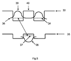
タイプ−I(直接バンドギャップ)MQW構造と比較すると、タイプ−II MQWは、電子と正孔の間の波動関数の重畳が小さいため、レーザまたはSOAの場合、一般に不利な利得媒体をもたらすと考えられている。図5は、分厚い障壁40を有するタイプ−II MQWバンド構造(電子バンド33および正孔バンド35)に対する第1の電子波動関数38および第1の正孔波動関数36を線図で示したものである。波動関数の重畳が小さいのは、電子波動関数38(したがって第1の電子レベル34)が個々の井戸39に閉じ込められ、一方、LHおよびHH波動関数36(したがって第1の正孔エネルギー準位37)は、障壁40中に閉じ込められることによるものである。J.B. Khurginら、IEEE Photonics Technol. Lett.、14巻、278〜280頁、2002年は、より長いキャリヤ平均寿命の結果としてのクロストークを小さくするために、Sbをベースとするひずみのないタイプ−II MQW SOAの使用を理論的に提案している。しかしながら、このような構造が有用な利得レベルを達成することができることを立証する試行はなされておらず、したがってほとんどのSOA用途に必要な低PDGを得るための設計の使用方法については示唆されていない。
Compared to a Type-I (Direct Bandgap) MQW structure, Type-II MQW is generally considered to provide a disadvantageous gain medium in the case of a laser or SOA due to the small superposition of wave functions between electrons and holes. It has been. FIG. 5 shows diagrammatically a first
R.Q. Yangら、IEEE J. Quantum Electrons、38巻、559〜568頁、2002年に、3μmから5μmまでのより長い中間赤外波長帯域では、半導体レーザを実現するために、InAs−InGaSbをベースとするタイプ−II MQW中のバンド間トンネリングを使用することができることが示されている。しかしながら半導体レーザのためのMQW設計の場合、低PDGを提供する必要はなく、したがって低PDGに対するこのような設計の効果は開示されていない。 R. Q. Yang et al., IEEE J. et al. Quantum Electrons, 38, 559-568, in 2002, in the longer mid-infrared wavelength band from 3 μm to 5 μm, in order to realize a semiconductor laser, in InAs-InGaSb based type-II MQW It has been shown that band-to-band tunneling can be used. However, in the case of MQW designs for semiconductor lasers, it is not necessary to provide a low PDG, and therefore the effect of such a design on a low PDG is not disclosed.
直接バンドギャップ遷移に基づくMQWデバイス
間接バンドギャップバンド構造の不適切性は、一般に、従来技術によるデバイスに、タイプ−Iに基づくバンド構造の使用をもたらし、したがって重い正孔遷移および軽い正孔遷移は、いずれも直接バンドギャップである。MQW利得構造は、デバイスが成長する際に、構造が基板に対してひずむように成長させることができる。原理的には任意の半導体層を他の半導体層の上に成長させることができるが、結晶構造を複数の層を通して継続するためには、格子定数を十分に整合させなければならない。構成元素が全く異なる半導体層の場合、実際には格子定数を十分に整合させることは困難であり、したがって実際には材料「システム」としてデバイスを成長させることが一般的であり、したがってQW層、障壁層および他の材料層中の構成元素のほとんどは同じであるが、異なるモル分率で形成される。
MQW devices based on direct bandgap transitions Inappropriate indirect bandgap band structures generally result in the use of band structures based on type-I in prior art devices, so heavy and light hole transitions are , Both are direct band gaps. The MQW gain structure can be grown such that the structure is distorted relative to the substrate as the device grows. In principle, any semiconductor layer can be grown on top of other semiconductor layers, but the lattice constant must be well matched to continue the crystal structure through multiple layers. In the case of semiconductor layers with completely different constituent elements, in practice it is difficult to match the lattice constants sufficiently, so in practice it is common to grow the device as a material “system” and thus the QW layer, Most of the constituent elements in the barrier layer and other material layers are the same but are formed in different molar fractions.
異なる半導体層を互いの上に成長させる場合、材料組成が異なることによって、堆積される層と、その下方の、利得媒体が成長する分厚い基板との間の格子定数が不整合になる可能性がある。堆積される層と基板層の間の格子定数が整合していない場合、堆積される層が引張りによってひずむか、あるいは圧縮によってひずむことになる。無ひずみ層の場合、軽い正孔および重い正孔に対する価電子帯端が退化するが、層にひずみが加えられると、軽い正孔および重い正孔に対する価電子帯端が分かれて、互いに遠ざかる方向に移動する。軽い正孔および重い正孔に対する価電子帯端が変化すると、個々の正孔の対応する閉込めが変化する。したがって特定の状況の下では、E−HH遷移をタイプ−IIにし、また、E−LH遷移をタイプ−Iにすることができる。 When different semiconductor layers are grown on top of each other, different material compositions can cause mismatch in the lattice constant between the deposited layer and the thicker substrate below which the gain medium is grown. is there. If the lattice constant between the deposited layer and the substrate layer is not matched, the deposited layer will be distorted by tension or by compression. In the case of an unstrained layer, the valence band edges for light and heavy holes degenerate, but when the layer is strained, the valence band edges for light and heavy holes are separated and moved away from each other. Move to. As the valence band edges for light and heavy holes change, the corresponding confinement of individual holes changes. Thus, under certain circumstances, the E-HH transition can be type-II and the E-LH transition can be type-I.
堆積層の組成を変更することにより、異なる量のひずみが導入される。ひずみの導入には、LHおよびHH価電子帯端エネルギー準位の退化を阻止する効果がある。層の組成を変化させることによってひずみの量およびタイプ(引張りまたは圧縮)を変更することにより、軽い正孔および重い正孔の量子化エネルギー準位、およびLHおよびHHの閉込めが変化し、延いては波動関数の重畳が変化する。したがってQW構造にひずみを導入することにより、TE偏光状態およびTM偏光状態に対する相対利得レベルを変更することができる。しかしながら、大量のひずみを徐々に導入すると、層に望ましくない欠陥が導入され、バンドギャップが変化し、また、軽い正孔遷移および重い正孔遷移に対する中心動作波長ピークが変化する。 By changing the composition of the deposited layer, different amounts of strain are introduced. The introduction of strain has the effect of preventing the degeneration of LH and HH valence band edge energy levels. Changing the amount and type of strain (tensile or compressive) by changing the composition of the layer changes the quantization energy levels of light and heavy holes, and the confinement of LH and HH, and In this case, the superposition of the wave function changes. Therefore, by introducing strain into the QW structure, the relative gain level for the TE polarization state and the TM polarization state can be changed. However, gradually introducing large amounts of strain introduces undesirable defects in the layer, changes the band gap, and changes the central operating wavelength peak for light and heavy hole transitions.
低PDG SOAを実現するための、ひずんだMQWを使用した多くの方法が報告されている。K. Magariら IEEE Photonics Technol. Lett. 2巻、556〜558頁、1990年に、MQWを利得媒体として使用した、障壁が引張りによってひずみ、また、井戸にひずみがない手法の1つが報告されている。K. Magariらは、厚さ10.5nmの無ひずみ量子井戸層、およびひずみが−1.7%(引張り)である厚さ11.5nmの障壁層を備えた利得媒体を使用している。SOAの長さは660μmであり、また、注入電流が200mAのファイバ利得のために1.0dBのPDGおよび13.0dBのファイバが提供されている。
Many methods using distorted MQW have been reported to achieve low PDG SOA. K. Magari et al., IEEE Photonics Technol. Lett.
M.A. Newkirkら IEEE Photonics Technol. Lett.、4巻、406〜408頁、1993年に、代替手法が報告されている。Newkirkは、ひずみが1.0%(圧縮)である厚さ3.5nmの3つの圧縮型井戸、ひずみが−1.0%(引張り)である厚さ16nmの3つの引張りひずみ井戸、および厚さ10nmの7つの無ひずみ障壁を備えた利得媒体を使用している。SOAの長さは625μmであり、また、注入電流が150mAのファイバ利得のために1.0dB未満のPDGおよび4.4dBのファイバが提供されている。 M.M. A. Newkirk et al., IEEE Photonics Technol. Lett. 4, 406-408, 1993, an alternative approach was reported. Newkirk has three compression wells with a thickness of 3.5 nm with a strain of 1.0% (compression), three tensile strain wells with a thickness of 16 nm with a strain of -1.0% (tensile), and a thickness. A gain medium with seven unstrained barriers of 10 nm is used. The SOA length is 625 μm and PDG less than 1.0 dB and 4.4 dB fiber are provided for a fiber gain of 150 mA injection current.
D. Sigogneら ECOC、267〜270頁、1995年に、他の手法が報告されており、Electron.Lett.、32巻、1403〜1405、1996年には、利得媒体として、ひずみが1.1%(圧縮)である厚さ8nmの16個の井戸、およびひずみが−0.9%(引張り)である厚さ7nmの16個の障壁が使用されている。SOAの長さは940μmであり、また、注入電流が150mAのファイバ利得のために1.0dB未満のPDGおよび23.0dBのファイバが提供されている。 D. Sigogne et al., ECOC, pp. 267-270, 1995, other techniques have been reported, Electron. Lett. 32, 1403-1405, 1996, as gain media, 16 wells with a thickness of 8 nm with a strain of 1.1% (compression), and a strain of -0.9% (tensile) Sixteen barriers with a thickness of 7 nm are used. The SOA length is 940 μm and PDG less than 1.0 dB and 23.0 dB fiber are provided for a fiber gain of 150 mA injection current.
タイプ−Iバンド構造を使用した上記従来技術の文書では、井戸および障壁のために使用されている材料は、InP基板の上に成長した、1.55μmの波長で動作するInGaAsまたはInGaAsPの組成に概ね基づいている。 In the above prior art document using the Type-I band structure, the materials used for the wells and barriers are InGaAs or InGaAsP compositions operating on 1.55 μm wavelength grown on InP substrates. Based mostly.
直接バンドギャップIn1−x−yAlxGayAs量子井戸を使用したOバンド動作のためのデバイス
1310nmの波長レンジで動作する、InPの上に成長したIn1−x−yAlxGayAsの組成を使用した利得媒体を備えたデバイスについては従来技術で説明した。1310nmの波長レンジで動作するレーザを記述している従来技術の文書の1つは、M. Yamadaら、IEEE、Photonics Technol. Lett.、11巻、164〜167頁、1999年によって記述されている。In1−x−yAlxGayAsからなる利得媒体のバンドギャップは、Alモル分率に対する依存性が極めて強い。バンドギャップが低Alモル分率を必要とする利得媒体をエピタキシャル成長させることは、事実上、困難である。したがってIn1−x−yAlxGayAs量子井戸を使用している従来技術は、1310nm帯域の近くに光波長が集中しているが、それは、この波長レンジでは、無ひずみ層に対する材料のAl含有量を、約15%を超えて維持することができ、したがって成長を容易に制御することができることによるものである。C. Zahら、IEEE J. Quantum Electronics、30巻、511〜522頁、1994年に、1310nmの近辺を中心とする波長レンジで動作するレーザの他の例が記述されている。しかしながらレーザは、TEモードまたはTMモードのいずれかで個々に偏光されるように設計されており、したがって一方の偏光で大きい利得を有し、また、それと直交する偏光では小さい利得を有するように設計されている。
Device for O-band operation using direct bandgap In 1-xy Al x Ga y As quantum wells In 1-xy Al x Ga y grown on InP operating in the 1310 nm wavelength range Devices with gain media using the composition of As have been described in the prior art. One prior art document describing a laser operating in the 1310 nm wavelength range is M.M. Yamada et al., IEEE, Photonics Technol. Lett. 11, pp. 164-167, 1999. The band gap of the gain medium made of In 1-xy Al x Ga y As is extremely dependent on the Al mole fraction. It is virtually difficult to epitaxially grow gain media whose band gap requires a low Al mole fraction. Thus, the prior art using In 1-xy Al x Ga y As quantum wells concentrates the light wavelength near the 1310 nm band, which means that in this wavelength range the material of the material for the unstrained layer This is because the Al content can be maintained above about 15% and thus the growth can be easily controlled. C. Zah et al., IEEE J. et al. Quantum Electronics, 30, 511-522, 1994 describes another example of a laser operating in a wavelength range centered around 1310 nm. However, the laser is designed to be individually polarized in either the TE mode or the TM mode, and thus has a large gain in one polarization and a small gain in the orthogonal polarization. Has been.
P. Koonathら、IEEE Photonics Technol. Lett.、13巻、779〜781頁、2001年に、1310nm波長の低PDG SOAが記述されている。Koonathでは、0.33%の引張りひずみを3つの量子井戸層に導入し、一方、障壁層を無ひずみにすることによって低PDGが実現されている。 P. Koonath et al., IEEE Photonics Technol. Lett. 13, 779-781, 2001, describes a low PDG SOA with a wavelength of 1310 nm. In Koonath, a low PDG is realized by introducing 0.33% tensile strain into the three quantum well layers while making the barrier layer unstrained.
デバイスを広く使用されている1550nmレンジ(Cバンド)などのより長い波長で動作させるためには、モル分率「x」の値が典型的には5%近辺になるように、In1−x−yAlxGayAs MQW中のAlの量を激減させなければならない。これらの条件の下では、材料のバンドギャップがAlモル分率に対して極めて敏感になるため、標準のタイプ−Iバンド構造を使用して低PDGデバイスを再現可能に得るために必要な制御のレベルを可能にするために、Alモル分率の十分な制御の下でInGaAlAsを成長させることは極めて困難である。 In order for the device to operate at longer wavelengths, such as the widely used 1550 nm range (C-band), the In 1-x is such that the value of the mole fraction “x” is typically around 5%. -y Al x Ga y As must be drastically reduced the amount of Al in the MQW. Under these conditions, the band gap of the material becomes very sensitive to the Al mole fraction, so the control required to obtain a low PDG device reproducibly using a standard Type-I band structure. It is extremely difficult to grow InGaAlAs under sufficient control of the Al mole fraction to allow levels.
1310nmレンジで動作する従来技術のレーザおよびSOAは、In1−x−yAlxGayAsの温度性能が改善されているにもかかわらず、重い正孔および軽い正孔の閉込めを変化させるためにひずみを導入することによって、同じく量子井戸のバンドギャップが変化するため、低PDG SOAの再現可能な製造は依然として問題である。さらに、1550nm近辺などのより長い波長レンジでは、製造可能にAlモル分率を制御することが困難になる。 Prior art lasers and SOAs operating in the 1310 nm range change heavy and light hole confinement despite improved temperature performance of In 1-xy Al x Ga y As Therefore, the reproducible production of low PDG SOAs is still a problem because introducing the strain also changes the band gap of the quantum well. Furthermore, in a longer wavelength range such as around 1550 nm, it becomes difficult to control the Al mole fraction in a manufacturable manner.
特許請求の範囲に詳しく記述されている本発明について説明する。 The present invention will be described in detail in the claims.
本発明によれば、入射光を受け取り、かつ、増幅された光を射出するための光増幅器が提供され、光増幅器は、入射光を受け取り、かつ、増幅された光を射出するための光導波路と、光利得を提供するための隣接する複数の半導体層を備えた利得媒体と、利得媒体を通じて電流をポンプするための電極とを備えており、隣接する複数の半導体層は、電子のための1つまたは複数の量子井戸を画定しており、また、利得媒体中における直接電子−正孔遷移および間接電子−正孔遷移の両方を提供するように動作し、それにより伝導帯中の第1の量子化電子エネルギー準位が第1の層中に位置し、価電子帯中の第1の量子化正孔エネルギー準位が前記第1の層中に位置し、価電子帯中の他の第1の量子化正孔エネルギー準位が隣接する第2の層中に位置し、第2の層は第1の層とは異なる材料組成を有し、第1の層中の第1の量子化正孔エネルギー準位は、軽い正孔状態か、あるいは重い正孔状態のいずれかであり、また、第2の層中の他の第1の量子化正孔エネルギー準位は、第1の層中の第1の量子化正孔エネルギー準位とは異なる正孔状態である。 According to the present invention, an optical amplifier is provided for receiving incident light and emitting amplified light, the optical amplifier receiving optical light for receiving incident light and emitting amplified light. And a gain medium comprising a plurality of adjacent semiconductor layers for providing optical gain, and an electrode for pumping current through the gain medium, wherein the plurality of adjacent semiconductor layers are for electrons Defines one or more quantum wells and operates to provide both direct electron-hole and indirect electron-hole transitions in the gain medium, thereby providing a first in the conduction band. The quantized electron energy level of the first valence band is located in the first layer, the first quantized hole energy level in the valence band is located in the first layer, and the other In a second layer adjacent to the first quantized hole energy level The second layer has a different material composition than the first layer, and the first quantized hole energy level in the first layer is either a light hole state or a heavy hole state. And the other first quantized hole energy level in the second layer is different from the first quantized hole energy level in the first layer. It is.
このような光増幅器は、スーパルミネセントダイオード(SLD)として使用することも可能であり、それによりデバイスによって生成され、かつ、デバイスから射出するASE光が光源として使用される。 Such an optical amplifier can also be used as a superluminescent diode (SLD), whereby ASE light generated by the device and emitted from the device is used as the light source.
光増幅器は、利得媒体が第1の光偏光のための第1のモード閉込め係数(MC1)および第2の光偏光のための第2のモード閉込め係数(MC2)を有するように構成することができ、MC1と、伝導帯中の第1の量子化電子エネルギー準位と第1の層の価電子帯中の第1の量子化正孔エネルギー準位の間の遷移からの利得との積は、MC2と、伝導帯中の第1の量子化電子エネルギー準位と第2の層の価電子帯中の他の第1の量子化正孔エネルギー準位の間の遷移からの利得との積の20%内で整合している。 The optical amplifier is configured such that the gain medium has a first mode confinement factor (MC1) for the first optical polarization and a second mode confinement factor (MC2) for the second optical polarization. MC1 and the gain from the transition between the first quantized electron energy level in the conduction band and the first quantized hole energy level in the valence band of the first layer. The product is MC2 and the gain from the transition between the first quantized electron energy level in the conduction band and the other first quantized hole energy levels in the valence band of the second layer. Is consistent within 20% of the product.
第2の層はIn1−x−yAlxGayAsを含んでいてもよい。 The second layer may include In 1-xy Al x Ga y As.
他の態様では、同じく本発明により、利得媒体を備えたデバイスが提供され、利得媒体は、光利得を提供するための隣接する複数の半導体層を備えており、隣接する複数の半導体層は、電子のための1つまたは複数の量子井戸を画定しており、利得媒体中における直接電子−正孔遷移および間接電子−正孔遷移の両方を提供するように動作し、それにより伝導帯中の第1の量子化電子エネルギー準位が第1の層中に位置し、価電子帯中の第1の量子化正孔エネルギー準位が前記第1の層中に位置し、価電子帯中の他の第1の量子化正孔エネルギー準位が隣接する第2の層中に位置し、第2の層は第1の層とは異なる材料組成を有し、第1の層中の第1の量子化正孔エネルギー準位は、軽い正孔状態か、あるいは重い正孔状態のいずれかであり、また、第2の層中の他の第1の量子化正孔エネルギー準位は、第1の層中の第1の量子化正孔エネルギー準位とは異なる正孔状態であり、第2の層はIn1−x−yAlxGayAs(x>0、y>0)を含んでいる。 In another aspect, the invention also provides a device comprising a gain medium, the gain medium comprising a plurality of adjacent semiconductor layers for providing optical gain, the plurality of adjacent semiconductor layers comprising: Defines one or more quantum wells for electrons and operates to provide both direct and indirect electron-hole transitions in the gain medium, thereby in the conduction band A first quantized electron energy level is located in the first layer, a first quantized hole energy level in the valence band is located in the first layer, and The other first quantized hole energy level is located in the adjacent second layer, the second layer having a different material composition than the first layer, and the first layer in the first layer The quantized hole energy level of either the light hole state or the heavy hole state The other first quantized hole energy level in the second layer is a hole state different from the first quantized hole energy level in the first layer, and the second The layer includes In 1-xy Al x Ga y As (x> 0, y> 0).
本発明は、半導体利得媒体(「能動領域/媒体」または光利得構造としても知られている)中の層の厚さおよび/または数を制御することにより、デバイス内のTE利得およびTM利得(または損失)の量を制御する問題に対処している。利得媒体の幅は、1μmおよび5μmを含むそれらの間であることが好ましい。利得媒体の幅は、1μmおよび2μmを含むそれらの間であることが好ましい。利得媒体の厚さは、0.1μmおよび0.2μmを含むそれらの間であることが好ましいが、他の利得媒体断面幾何構造を使用することも可能である。 The present invention controls the TE gain and TM gain in a device (by controlling the thickness and / or number of layers in a semiconductor gain medium (also known as an “active region / media” or optical gain structure). Or dealing with the problem of controlling the amount of loss). The width of the gain medium is preferably between those including 1 μm and 5 μm. The width of the gain medium is preferably between those including 1 μm and 2 μm. The gain medium thickness is preferably between those including 0.1 μm and 0.2 μm, although other gain medium cross-sectional geometries can be used.
本発明のデバイスは、図1に示されている埋設へテロ構造導波路構造を備えることができ、埋設へテロ構造導波路構造は、利得媒体10を覆っているp−型キャップ層9(典型的にはInPからなる)およびn−型層11(典型的にはInPからなる)を備えた垂直メサ、メサの下方のn−型クラッド層6およびn−型基板7(典型的にはInPからなる)、メサの両側に配置された1つまたは複数のn−型ブロック層4(典型的にはInPからなる)およびp−型ブロック層5(典型的にはInPからなる)、メサおよび1つまたは複数のブロック層を覆っているp−型層3(典型的にはInPからなる)、層3のすぐ上のコンタクト層2、コンタクト層2の上に配置された上部電極1、および基板7の下方に配置された下部電極8を備えている。
The device of the present invention can comprise the buried heterostructure waveguide structure shown in FIG. 1, which is a p-type cap layer 9 (typically covering the gain medium 10). A vertical mesa with a n-type layer 11 (typically made of InP), an n-type cladding layer 6 under the mesa and an n-type substrate 7 (typically InP). One or more n-type blocking layers 4 (typically composed of InP) and p-type blocking layers 5 (typically composed of InP) disposed on both sides of the mesa, A p-type layer 3 (typically made of InP) covering one or more blocking layers, a
別法としては、デバイスは、図2に示されているリッジ型導波路構造を備えることも可能であり、リッジ型導波路構造は、n−型基板18(典型的にはInPからなる)、基板18の上に位置している利得媒体17、利得媒体17のすぐ上のp−型クラッド層16、クラッド層16の上のp−型層14であって、窒化ケイ素層15、20によって両側が取り囲まれた垂直メサを形成するためにパターン化され、かつ、エッチングされるp−型層14、p−型層14の上のコンタクト層13、コンタクト層13を覆っている上部電極12、および基板18の下方の下部電極19を備えている。
Alternatively, the device can comprise a ridge-type waveguide structure as shown in FIG. 2, which comprises an n-type substrate 18 (typically made of InP), A
上記2つの構造は、本発明のデバイスを形成することができる方法の単なる好ましい例にすぎない。他の適切な構造を使用することも可能である。 The above two structures are merely preferred examples of how the devices of the present invention can be formed. Other suitable structures can also be used.
本発明の一例によれば、入射光を受け取り、かつ、増幅された光を射出するための光導波路、光利得を提供するための隣接する複数の半導体層を備えた利得媒体、および利得媒体を通じて電流をポンプするための電極1を備えた光増幅器が提供される。隣接する複数の半導体層は、電子のための1つまたは複数の量子井戸を画定している。伝導帯中の第1の量子化電子エネルギー準位および価電子帯中の第1の量子化正孔エネルギー準位は、第1の層(第1の半導体材料層)中に位置している。価電子帯中の他の第1の量子化正孔エネルギー準位は、隣接する第2の層(第2の半導体材料層)中に位置している。第2の層は第1の層とは異なる材料組成を有する。
In accordance with an example of the present invention, an optical waveguide for receiving incident light and emitting amplified light, a gain medium with a plurality of adjacent semiconductor layers for providing optical gain, and through the gain medium An optical amplifier with an
利得媒体は、導波路の一部であっても/導波路と一体であってもよく、あるいは導波路とは別であってもよい。第1の層中の第1の量子化正孔エネルギー準位および第2の層中の他の第1の量子化正孔エネルギー準位は、それぞれ最大重い正孔エネルギー準位または最大軽い正孔エネルギー準位のうちのいずれかと呼ばれている(あるいは第1の重い正孔レベルおよび第1の軽い正孔レベルと呼ばれている)。実際は、量子井戸中の電子の最小エネルギー準位(すなわち基底状態)は、帯端に最も近いレベルであり、また、量子井戸中の正孔に対しては、価電子帯に最も近いエネルギー準位は、同じく正孔に対する最小エネルギー準位(すなわち基底状態)である。しかしながら、この文書では、線図に対するテキストの理解を容易にするために、量子井戸中の電子の最も低いエネルギー状態すなわち基底状態を表すために電子最小エネルギー準位が使用されており、また、価電子帯端に最も近い正孔状態すなわち基底状態を表すために正孔最大エネルギー準位が使用されており、つまりエネルギーの増加は、線図中では常に上に向かっている(電子および正孔の両方に対して)。 The gain medium may be part of the waveguide / integral with the waveguide, or may be separate from the waveguide. The first quantized hole energy level in the first layer and the other first quantized hole energy level in the second layer are the maximum heavier hole energy level or the lightest hole, respectively. It is called one of the energy levels (or called the first heavy hole level and the first light hole level). In fact, the minimum energy level (ie, ground state) of electrons in the quantum well is the level closest to the band edge, and for holes in the quantum well, the energy level closest to the valence band. Is also the minimum energy level (ie, ground state) for holes. However, this document uses the minimum electron energy level to represent the lowest energy state of the electrons in the quantum well, ie, the ground state, in order to facilitate the understanding of the text for the diagram. The hole maximum energy level is used to represent the hole state closest to the electron band edge, ie, the ground state, ie, the energy increase is always upward in the diagram (electron and hole For both).
デバイスは、原理的には、複数の異なるタイプの半導体材料からなる光利得を提供するのに適した媒体を備えた任意の光増幅器であってもよい。デバイスは半導体光増幅器であることが好ましい。SOAは、導波路から光が射出するデバイスの長さの末端に、少なくとも1つ、好ましくは2つの無反射コートファセットを備えていることが好ましい。端ファセットには、端ファセットで反射したすべての光が導波路内を逆方向に伝搬しないように、デバイスの平面に好ましくは7°と10°の間の角度を付けることができる(角度が付いた導波路は、必要な特徴ではないが、残留反射を小さくするのを促進する)。本出願の目的のための材料「層」という用語の層は、任意の断面幾何構造に関連しているが、一方の主寸法がもう一方の主寸法より長い矩形をベースとする断面であることが好ましい。通常、基板ウェーハの上にデバイスを成長させ、それにより「層」の幅がウェーハの平面に対して平行になり、この幅は厚さより大きい。デバイスは、原理的には任意の知られている半導体製造方法を使用して形成することができ、有機金属気相エピタキシ(MOVPE)が好ましい。 The device may in principle be any optical amplifier with a medium suitable for providing an optical gain composed of a plurality of different types of semiconductor materials. The device is preferably a semiconductor optical amplifier. The SOA preferably comprises at least one, preferably two anti-reflective coated facets at the end of the length of the device from which light exits the waveguide. The end facets can be angled preferably between 7 ° and 10 ° in the plane of the device so that all light reflected at the end facets does not propagate backwards in the waveguide. The waveguide is not a necessary feature, but helps to reduce residual reflection). The term material “layer” for purposes of this application is a cross section based on a rectangle that is associated with any cross-sectional geometry, but one major dimension is longer than the other major dimension. Is preferred. Typically, the device is grown on a substrate wafer so that the width of the “layer” is parallel to the plane of the wafer and this width is greater than the thickness. The device can in principle be formed using any known semiconductor manufacturing method, with metalorganic vapor phase epitaxy (MOVPE) being preferred.
MQWスタックを形成している第1および第2の層は、量子力学的に結合されており、互いに接触して隣接していることが好ましいが、原理的には1つまたは複数の他の異なる層をそれらの間に介在させることができる。利得媒体は、第1および第2の層以外の他の材料層を備えることができる。本発明は、複数の第1の層および/または複数の第2の層を備えていることが好ましい。第1および第2の層はMQWスタックを形成していることが好ましく、それにより複数の1つのタイプの層が、1つまたは複数の他のタイプの層に交互にはさまれる。第1および第2の層は、任意の厚さにすることができるが、2nmと15nmの間の厚さからなっていることが好ましい。利得媒体は、通常、頂部および底部で、利得媒体全体にわたるp−n接合の形成を可能にする1つまたは複数の個別の閉込めヘテロ構造(SCH)層と隣接している。 The first and second layers forming the MQW stack are preferably quantum mechanically coupled and preferably in contact with and adjacent to each other, but in principle one or more other different Layers can be interposed between them. The gain medium can comprise other material layers than the first and second layers. The present invention preferably includes a plurality of first layers and / or a plurality of second layers. The first and second layers preferably form an MQW stack, whereby a plurality of one type of layers are alternately sandwiched by one or more other types of layers. The first and second layers can be of any thickness, but preferably have a thickness between 2 nm and 15 nm. The gain medium is typically adjacent at the top and bottom with one or more individual confinement heterostructure (SCH) layers that allow the formation of a pn junction across the gain medium.
対応する第1および第2の層中の第1の量子化正孔エネルギー準位と他の第1の量子化正孔エネルギー準位の空間分離は、通常、これらの層のうちの1つまたは複数にひずみを導入し、かつ、バンドギャップを適切に選択することによって達成される。適切な量のひずみを層に加えることによって電子量子井戸として作用し、重い価電子帯端エネルギー準位および軽い正孔価電子帯端エネルギー準位が離れる方向に移動し、したがって第1の材料層中の一方の正孔タイプの価電子帯端エネルギーが第2の材料層中の同じ正孔タイプの価電子帯端エネルギーより大きくなり、一方、第1の材料層中のもう一方の正孔タイプの価電子帯端エネルギーは、第2の材料層中の同じ正孔タイプの価電子帯端エネルギーより小さくなる。個々の正孔に対する最大価電子帯端エネルギーは異なる層に存在するため、第1の層は、一方のタイプの正孔のための量子井戸になり、一方、第2の層は、もう一方のタイプの正孔のための量子井戸になる。 Spatial separation of the first quantized hole energy level and the other first quantized hole energy level in the corresponding first and second layers is usually one of these layers or This is achieved by introducing strain into a plurality and appropriately selecting the band gap. Acting as an electron quantum well by applying an appropriate amount of strain to the layer, moving the heavy valence band edge energy level and the light hole valence band edge energy level away, thus the first material layer The valence band edge energy of one hole type in the second material layer is greater than the valence band edge energy of the same hole type in the second material layer, while the other hole type in the first material layer The valence band edge energy of is less than the valence band edge energy of the same hole type in the second material layer. Because the maximum valence band edge energy for individual holes exists in different layers, the first layer becomes a quantum well for one type of hole, while the second layer becomes the other. Become a quantum well for the type of holes.
したがって、重い正孔および軽い正孔の両方に対してタイプ−Iの遷移、または重い正孔および軽い正孔の両方に対してタイプ−IIの遷移のいずれかを有していた従来技術によるデバイスとは対照的に、本発明によれば、直接遷移および間接遷移の両方を提供する利得媒体を備えた光増幅器が提供される。重い正孔および軽い正孔がタイプ−Iの遷移またはタイプ−IIの遷移のいずれかである場合、相対HHおよびLH波動関数閉込めを変化させるために必要なひずみが、a)個々の遷移のピーク波長の望ましくない変化の原因になり、そのためにデバイスの最適動作値が逸脱することになる可能性がある、および/またはb)過度に大きくなり、そのためにデバイス製造中に材料欠陥が生じ、デバイスの性能が低下することになる。材料層中の大量のひずみは、成長および緩和の際に層を不安定にし、そのため、過剰な非発光再結合中心が形成される原因になる極めて多数の転位が形成されることになる。このような非発光再結合中心は、SOAまたは半導体レーザなどのデバイスを実現するための十分な自然放出の生成には不適切な材料を構築することになる。 Thus, prior art devices that had either type-I transitions for both heavy and light holes, or type-II transitions for both heavy and light holes In contrast, the present invention provides an optical amplifier with a gain medium that provides both direct and indirect transitions. When heavy and light holes are either Type-I transitions or Type-II transitions, the strains required to change the relative HH and LH wavefunction confinement are: a) Which can cause undesirable changes in peak wavelength and therefore deviate from the optimal operating value of the device, and / or b) become excessively large, which results in material defects during device manufacturing, Device performance will be degraded. A large amount of strain in the material layer can cause the layer to become unstable during growth and relaxation, thus forming a large number of dislocations that cause the formation of excess non-radiative recombination centers. Such non-emissive recombination centers will construct materials that are unsuitable for generating sufficient spontaneous emission to realize devices such as SOAs or semiconductor lasers.
利得媒体中に、タイプ−I(直接バンドギャップ)遷移として1つの電子−正孔遷移を有し、かつ、タイプ−II(間接バンドギャップ)遷移として他の電子−正孔遷移を有することにより、利得媒体中の軽い正孔および重い正孔に対する波動関数ピークが層の厚さ全体にわたって空間的にオフセットされることになる(ウェーハ層の平面に対して直角に)。E−LH遷移に対するE−HH遷移の相対量(したがってTE利得およびTM利得の相対量)は、第1および第2の層の各々の厚さの比率を変化させることによって変えることができる。また、電子遷移の相対量も、第2の層に対する第1の層の数を変えることによって変化させることができる。 By having one electron-hole transition as a Type-I (direct bandgap) transition and another electron-hole transition as a Type-II (indirect bandgap) transition in the gain medium, The wave function peaks for light and heavy holes in the gain medium will be spatially offset throughout the layer thickness (perpendicular to the plane of the wafer layer). The relative amount of E-HH transition relative to the E-LH transition (and thus the relative amount of TE gain and TM gain) can be varied by changing the ratio of the thickness of each of the first and second layers. Also, the relative amount of electronic transition can be varied by changing the number of first layers relative to the second layer.
LH波動関数ピークおよびHH波動関数ピークは、空間的に分離されている最小価電子帯端に基づいて互いに空間的にオフセットされるため、第1および第2の層の相対厚さが変化すると、HH波動関数およびLH波動関数の相対閉込めが変化する。HH波動関数およびLH波動関数の相対閉込めが変化すると、LH−E波動関数(TM利得を提供している)とは異なる方法でHH−E波動関数重畳(TEを提供している)が変化する。したがって本発明によれば、E−波動関数を使用してHH波動関数およびLH波動関数の相対重畳を制御するための追加手段が提供され、したがって望ましくない、あるいは不利な値のひずみを必ずしも層中に必要とすることなく、TE利得およびTM利得を平衡させるための機構が提供される。TE/TM利得をある程度余裕をもって制御することにより、デバイスの製造者は、小さい値のひずみを使用して適切なバンドギャップをより自由に選択することができる。 Since the LH wave function peak and the HH wave function peak are spatially offset from each other based on the spatially separated minimum valence band edge, the relative thickness of the first and second layers changes, The relative confinement of the HH and LH wave functions changes. When the relative confinement of the HH and LH wavefunctions changes, the HH-E wavefunction superposition (provides TE) changes in a different way than the LH-E wavefunction (provides TM gain) To do. Thus, according to the present invention, an additional means for controlling the relative superposition of the HH and LH wave functions using the E-wave function is provided, and therefore undesirable or adverse values of distortion are not necessarily in the layer. A mechanism is provided for balancing TE gain and TM gain without the need for By controlling the TE / TM gain with some margin, the device manufacturer can more freely select an appropriate bandgap using a small value of distortion.
引き続いて本発明の上記の例を参照すると、本発明の発明者らは、さらに、第1の材料層中の伝導帯端エネルギー準位が第2の材料層中の伝導帯端エネルギー準位より小さく、かつ、第1の材料層が引張りひずみを備えている場合、軽い正孔を第1の材料層に量子閉込めすることができ、一方、重い正孔は、第2の材料層に量子閉込めされ、したがってE/HH遷移は間接遷移であり、また、E/LH遷移は直接遷移であることを見出した。 Continuing with reference to the above example of the present invention, the inventors further demonstrate that the conduction band edge energy level in the first material layer is greater than the conduction band edge energy level in the second material layer. If small and the first material layer has tensile strain, light holes can be quantum confined to the first material layer, while heavy holes are quantum confined to the second material layer. It has been found that the E / HH transition is confined and therefore the E / HH transition is an indirect transition and the E / LH transition is a direct transition.
この構造の場合、第1の材料層が電子および軽い正孔に対する量子井戸になり、また、第2の材料層が電子および軽い正孔に対する障壁になり、一方、第2の材料層は、重い正孔に対する量子井戸になり、また、第1の材料層は、重い正孔に対する障壁になる。この構造の場合、第1の材料の1つまたは複数の層が第2の材料の1つまたは複数の層に交互にはさまれ、これらの層と隣接していることが好ましい。第2の材料の1つまたは複数の追加層は、「n」番目の第1の層をn+1番目の第2の層、n番目の第2の層またはn−1番目の第2の層によって境界を画することができるように、第1の材料の最も外側の層の外側に隣接させることができる。 For this structure, the first material layer is a quantum well for electrons and light holes, and the second material layer is a barrier for electrons and light holes, while the second material layer is heavy. It becomes a quantum well for holes, and the first material layer becomes a barrier for heavy holes. For this structure, it is preferred that one or more layers of the first material are alternately sandwiched by and adjacent to one or more layers of the second material. The one or more additional layers of the second material may include an “n” th first layer by an (n + 1) th second layer, an nth second layer, or an (n−1) th second layer. It can be adjacent to the outside of the outermost layer of the first material so that a boundary can be defined.
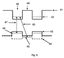
一例として、図6は、本発明によるデバイスのバンド構造の略線図を示したものである。この線図には、電子(電子帯端41および第1の電子レベル42)および軽い正孔(軽い正孔帯端43および第1の軽い正孔レベル46)を閉じ込めている第1の材料の2つの層と、重い正孔(重い正孔帯端44および第1の重い正孔レベル45)を閉じ込めている第2の材料のただ1つの層が存在する。線図で示されているこの構造には、TM利得に寄与している2つの軽い正孔「井戸」と、TE利得に寄与しているただ1つの重い正孔「井戸」が存在する。しかしながら、他の2つの第2の層を構造に導入することにより、TE材料利得に寄与するn+1個の重い正孔「井戸」が存在することになる。
As an example, FIG. 6 shows a schematic diagram of the band structure of a device according to the invention. This diagram shows the first material confining electrons (
実際には、利得媒体は、一般にTEOおよびTMOと呼ばれている最も低いTEモードおよびTMモードのみをサポートすることが望ましい。その結果、利得媒体の幅および厚さ全体を調整するための余地が若干残される。したがって可能な限り多くの利得媒体設計の自由を有することが有利である。本発明の場合、個々の層の数および厚さを変更することができるため、構造の設計者は、最適な層の厚さおよび数を選択する大きい自由度を有し、したがって材料層の組成を適切なバンドギャップに調整することができ、また、最小量のひずみを使用して重い正孔を間接遷移にし、軽い正孔を直接遷移にすることができる。 In practice, it is desirable for the gain medium to support only the lowest TE and TM modes, commonly referred to as TEO and TMO. As a result, there remains some room for adjusting the overall width and thickness of the gain medium. It is therefore advantageous to have as many gain media design freedoms as possible. In the case of the present invention, the number and thickness of the individual layers can be varied, so that the structure designer has a great degree of freedom in selecting the optimum layer thickness and number and thus the composition of the material layers Can be adjusted to an appropriate bandgap, and a minimum amount of strain can be used to make heavy holes indirect transitions and light holes to direct transitions.
E波動関数38は、その存在が第2の層中に限定されているため(図5参照)、HH波動関数が主として1つまたは複数の第2の層中に位置している場合、E−HH波動関数重畳は小さい。この小さいE−HH波動関数重畳を大きくするためには、場合によってはこれらの層と層の間のより強力な量子結合が必要である。この強力な量子結合は、複数の第2の層のうちの1つまたは複数の厚さを薄くすることによって達成することができ、一般的には10nm未満の厚さまで薄くすることによって達成することができる。図7は、バンド構造(電子バンド51、重い正孔バンド53)を概略的に示したもので、より薄い第2の層(第1の重い正孔エネルギー準位55を有する障壁58)は、利得媒体中の電子波動関数56および第1の重い正孔波動関数54に対する効果を有する。第1の層(井戸57)は、第1の(最小)電子エネルギー準位52を使用して、強力に量子力学結合されるようになり、したがってE波動関数56は、かなりの程度まで第2の層(障壁58)中に侵入する。その結果、E波動関数56がかなりの程度までHH波動関数54と重畳してTE利得を大きくする。
Since the
引き続いて本発明の任意の上記の例を参照すると、本発明の発明者らは、さらに、第1の材料層が引張りによってひずみ、電子および軽い正孔に対する量子井戸として作用し、また、第2の材料層がIn1−x−yAlxGayAs(x>0、y>0)を含む場合、第1の層と第2の層の間のバンドオフセット分割比は約70/30であることを見出した。この分割比は、名目上、電子が正孔よりかなりの程度まで閉じ込められることを意味する。第2の材料層は、引張りひずみまたは圧縮ひずみの下で無ひずみ(0%ひずみ)にすることができる。1つまたは複数の第1の材料層のうちの1つまたは複数の層中の引張りひずみは、0.5%と2.0%の間であることが好ましい。1つまたは複数の第2の材料層のうちの1つまたは複数の層中のひずみは、0.3%引張りひずみと0.3%圧縮ひずみの間であることが好ましい。第2の材料層は、In1−x−yAlxGayAs(0<x<=0.48、0<y<0.6)を含むことが好ましい。第2の材料層は、In1−x−yAlxGayAs(0<x<=0.4)(0<y<0.6)を含むことが好ましい。 With continued reference to any of the above examples of the present invention, the inventors of the present invention further demonstrate that the first material layer acts as a quantum well for strain, electrons and light holes due to tension, and second When the material layer includes In 1-xy Al x Ga y As (x> 0, y> 0), the band offset division ratio between the first layer and the second layer is about 70/30. I found out. This split ratio nominally means that electrons are confined to a much greater extent than holes. The second material layer can be unstrained (0% strain) under tensile or compressive strain. The tensile strain in one or more of the one or more first material layers is preferably between 0.5% and 2.0%. The strain in one or more of the one or more second material layers is preferably between 0.3% tensile strain and 0.3% compressive strain. The second material layer preferably includes In 1-xy Al x Ga y As (0 <x <= 0.48, 0 <y <0.6). The second material layer preferably includes In 1-xy Al x Ga y As (0 <x <= 0.4) (0 <y <0.6).
電子は実効質量がより小さいため、正孔と比較すると、電子はそれほど量子井戸に閉じ込められない。大きい電位障壁を量子井戸の両側に使用してより多くの電子を閉じ込めるほど、電子波動関数および正孔波動関数がより良好に重畳し、それにより、とりわけデバイスが高温で動作している場合に発光(光放出)再結合効率が改善される。したがって伝導帯に有利なオフセット分割比を有することが望ましい(例えば70/30の分割比は、60/40のオフセット分割比よりもかなりの程度まで電子を閉じ込めることになる)。利得構造がIn1−x−yAlxGayAs「システム」を含むように、1つまたは複数の第1および第2の層は、いずれもIn1−x−yAlxGayAsを含んでいることが好ましいが、原理的には、第2の層と共に首尾よく成長させることができることを条件として任意の他の材料を第1の層に使用することができ、所望のバンドギャップおよびオフセット分割比を提供することができる。第1の材料層は、In1−x−yAlxGayAs(x=>0、y>0である)を含んでいてもよい。第1の材料層は、In1−x−yAlxGayAs(0<=x<=0.48、0<y<0.6)を含んでいることが好ましい。第1の材料層は、In1−x−yAlxGayAs(0<=x<=0.4)(0<y<0.6)を含んでいることが好ましい。通常、In1−x−yAlxGayAs「システム」のための基板はInPである。 Since electrons have a smaller effective mass, electrons are less confined in quantum wells than holes. The more potential electrons are confined using a large potential barrier on either side of the quantum well, the better the electron and hole wavefunctions overlap so that they emit light, especially when the device is operating at high temperatures. (Light emission) Recombination efficiency is improved. It is therefore desirable to have an offset split ratio that is advantageous for the conduction band (eg, a 70/30 split ratio will confine electrons to a much greater extent than an 60/40 offset split ratio). The one or more first and second layers are both In 1-xy Al x Ga y As so that the gain structure includes the In 1-xy Al x Ga y As “system”. In principle, any other material can be used for the first layer, provided that it can be successfully grown with the second layer, with the desired band gap and An offset split ratio can be provided. The first material layer may include In 1-xy Al x Ga y As (x => 0, y> 0). The first material layer preferably contains In 1-xy Al x Ga y As (0 <= x <= 0.48, 0 <y <0.6). The first material layer preferably contains In 1-xy Al x Ga y As (0 <= x <= 0.4) (0 <y <0.6). Typically, the substrate for the In 1-xy Al x Ga y As “system” is InP.
第2の層がIn1−x−yAlxGayAs(x>0、y>0)を含んでいる場合、デバイスは光増幅器に限定されないが、原理的には光利得媒体を備えた任意のデバイスであってもよい。 If the second layer comprises In 1-xy Al x Ga y As (x> 0, y> 0), the device is not limited to an optical amplifier, but in principle comprises an optical gain medium. Any device may be used.
したがってIn1−x−yAlxGayAs「システム」を使用している本発明のデバイスによれば、40/60未満のオフセット分割比を有するIn1−xGaxAsyP1−yシステムを使用している等価デバイスより高い効率および温度無依存性が提供される。 Thus, according to the device of the present invention using the In 1-xy Al x Ga y As “system”, an In 1-x Ga x As y P 1-y having an offset split ratio of less than 40/60. Higher efficiency and temperature independence are provided than equivalent devices using the system.
また、In1−x−yAlxGayAs「システム」を使用している本発明のデバイスによれば、より優れた柔軟性が提供され、In1−xGaxAsシステムより層のひずみを小さくすることができ、第1および第2の材料は、いずれもIn1−xGaxAsの異なる組成を含んでいる。ガリウム(Ga)含有量が変化すると、インジウム(In)含有量およびひずみが自動的に変化するため、In1−xGaxAsシステムにおけるひずみおよびバンドギャップは直接リンクされる。したがってIn1−xGaxAsシステムにおける層中のひずみは、その層に対する必要なバンドギャップによって指示される。しかしながら、In1−x−yAlxGayAs「システム」を使用している本発明のデバイスは、Al含有量およびGa含有量の両方を変化させて所望のバンドギャップおよび層ひずみを得ることができ、つまり余分の自由度が存在するため、選択された層バンドギャップに対する様々な値の層ひずみを有する層を有することができる。 Also, the device of the present invention using the In 1-xy Al x Ga y As “system” provides greater flexibility and layer strain than the In 1-x Ga x As system. The first and second materials both contain different compositions of In 1-x Ga x As. As the gallium (Ga) content changes, the indium (In) content and strain automatically change, so the strain and band gap in the In 1-x Ga x As system are linked directly. Thus, the strain in a layer in the In 1-x Ga x As system is dictated by the required band gap for that layer. However, the device of the present invention using the In 1-xy Al x Ga y As “system” can vary both Al and Ga contents to obtain the desired band gap and layer strain. In other words, since there is an extra degree of freedom, it is possible to have layers with different values of layer strain for the selected layer band gap.
したがってIn1−x−yAlxGayAs「システム」を使用している本発明のデバイスによれば、より高い電子閉込めの利点と、ひずみおよびバンドギャップの減結合の利点の望ましい組合せが提供され、したがって小さい値のひずみを1つまたは複数の第1の層に使用して効率が高いデバイスを製造することができる。さらに、約70/30の分割比のため、正孔に対するより大きい閉込めを与えるオフセット比率を有するIn1−x−yGaxAsyPシステムなどのシステムと比較すると、第1および第2の層の名目上無ひずみの価電子帯端間のエネルギー準位の差(したがって閉込め)が小さい。したがって第1および第2の層の価電子帯端間のエネルギーの差が小さいほど、第1の層中の重い正孔価電子帯端エネルギーを第2の層中の重い正孔価電子帯端エネルギー未満に降下させるために必要な引張りひずみが小さくなり、したがってE−HH遷移に対してタイプ−IIの挙動が提供される。 Thus, the device of the present invention using the In 1-xy Al x Ga y As “system” provides a desirable combination of higher electron confinement benefits and strain and bandgap decoupling benefits. Provided, therefore, a low value of strain can be used in one or more first layers to produce a highly efficient device. Furthermore, because of the split ratio of about 70/30, the first and second compared to a system such as an In 1-xy Ga x As y P system with an offset ratio that provides greater confinement to holes The difference in energy levels (thus confinement) between the nominally unstrained valence band edges of the layer is small. Therefore, the smaller the energy difference between the valence band edges of the first and second layers, the heavier hole valence band edge energy in the first layer becomes. Less tensile strain is required to drop below energy, thus providing Type-II behavior for the E-HH transition.
好ましい例
5つの「井戸」48および6つの「障壁」49からなる利得構造を使用してデバイスが製造された。「井戸」48は、それぞれ11nmの厚さになるように成長され、一方、「障壁」は、7nmの厚さになるように成長され、個々の「井戸」と「井戸」の間は、単一の「障壁」が成長された。利得媒体のすぐ上および下方はSCH層であった。
Preferred Example A device was fabricated using a gain structure consisting of five “wells” 48 and six “barriers” 49. The “wells” 48 are each grown to a thickness of 11 nm, while the “barriers” are grown to a thickness of 7 nm, with a single “well” between each “well” and “well”. A “barrier” has grown. Immediately above and below the gain medium was the SCH layer.
この例ではデバイスはSOA(半導体光増幅器)であるが、原理的には、半導体利得/損失媒体を備えた任意のデバイスであってもよい。SOA利得媒体は、In1−x−yAlxGayAsの第1の層48(「井戸」)およびIn1−x−yAlxGayAsの第2の層49(「障壁」)を交互に備えたIn1−x−yAlxGayAs MQWスタックを備えている。井戸は、障壁49より小さいバンドギャップエネルギーを有する。井戸材料の組成は、井戸48および障壁49に対して、1550nm近辺の波長ピークに対するバンドギャップ、井戸層48中の引張りひずみ、および無ひずみ障壁49が得られるように選択される。井戸48中の引張りひずみによって軽い正孔および重い正孔の井戸価電子帯端エネルギーの退化が阻止され、したがって重い正孔帯端が、事実上、下に向かって「押され」て電子バンドから離れ、また、軽い正孔帯端が、事実上、電子バンドに向かって引っ張られる。障壁は、概ね無ひずみになるように成長されるため、障壁に対する重い正孔バンドおよび軽い正孔バンドが退化する。電子−軽い正孔遷移47は直接バンドギャップ(タイプ−I)遷移になり、一方、電子−重い正孔遷移50は間接バンドギャップ(タイプ−II)遷移である。
In this example, the device is a SOA (semiconductor optical amplifier), but in principle it may be any device with a semiconductor gain / loss medium. The SOA gain medium includes In 1-xy Al x Ga y As first layer 48 (“well”) and In 1-xy Al x Ga y As second layer 49 (“barrier”). and a in 1-x-y Al x Ga y As MQW stack with alternating. The well has a band gap energy smaller than the
Table 1(表1)は、デバイスの層の組成、ひずみおよび厚さを詳細に示したものである。 Table 1 (Table 1) details the layer composition, strain and thickness of the device.

図8は、理論的バンド構造(電子バンド59、重い正孔バンド61、軽い正孔バンド62)、および好ましい例のデバイスの計算波動関数を略図で示したものである。伝導帯の場合、第1の電子エネルギー準位波動関数64は、事実上、第1の「井戸」材料の5つの層に対応する5つの量子井戸を見ており、したがって5つのピークを有する。同様に、第1の軽い正孔エネルギー準位波動関数63も同じく5つの量子井戸を見ており、したがって同じく5つのピークを有する。しかしながら、第2の「障壁」材料の6つの層が存在するため、第1の重い正孔エネルギー準位波動関数60は6つの量子井戸を見ており、したがって6つのピークを備えている。したがってこのデバイスには、g(TM)に寄与する5つの量子井戸、およびg(TE)に寄与する6つの量子井戸が存在する。「井戸」(第1の層)および「障壁」(第2の層)の厚さは、量子井戸が良好に量子力学結合されるように、適切に選択された。
FIG. 8 schematically shows the theoretical band structure (electron band 59,
MOVPEおよび標準リソグラフィ技法ならびにエッチング技法を使用して、table 1(表1)の層構造を備えた多重BH SOAデバイスが製造された。これらのデバイスは、InPウェーハの上に形成された。製造が完了すると、個々のSOAデバイスが長さ0.88mmのバーにへき開され、かつ、両方の端ファセットに無反射コーティングが施された。 Multiple BH SOA devices with the layer structure of table 1 (Table 1) were fabricated using MOVPE and standard lithography techniques as well as etching techniques. These devices were formed on InP wafers. When manufacturing was complete, the individual SOA devices were cleaved into 0.88 mm long bars, and both end facets were anti-reflective coated.
個々のデバイスは、平面形状が矩形であり、n−型になるようにドープされたInP「クラッド」層6と共にオーバグロースされたInP基板を備えていた。次に、幅5μmのInPをベースとする受動導波路がクラッド層の上に形成された。受動導波路は、効率が高い入力/出力結合を得るために末端がレンズのファイバであることが好ましい光ファイバとモード整合するように設計された。次に、一方の端ファセット部分の0.3μmからチップの中央部分の1.3μmまで、直線的に先太りのテーパが施された幅を有する一連の直立メサを形成するために、受動導波路の上にtable 1(表1)の層が成長され、パターン化され、かつ、エッチングされた。次に、1.3μmから反対側の端ファセット部分の0.3μmの幅まで、今度は先細りのテーパが施された。ファセット部分の狭い幅からデバイスの中部分のより広い幅まで利得媒体をテーパ化することにより、受動導波路に入射する光が光利得のためにデバイスの中央で利得媒体に結合し、次に、高いファイバ結合効率をファット部分に提供するためにもう一度受動導波路に結合することが確実にされる。メサは、後方反射を小さくするために、端ファセットから端ファセットまで走っているメサの長さが、ファセットに対して直角の方向から10度の角度だけ外れるようにパターン化された。次にメサの側壁に沿って電流阻止層を提供するために、半導体材料のオーバグロースを使用してメサが覆われた。p−型ZnドープInPの5μmの層を成長させ、引き続いてZnが高度にドープされたInGaAs p−コンタクト層を成長させることによってメサが埋設された。次に、デバイスの評価を可能にするためにデバイスが電気結合された。光利得、PDGおよび他のパラメータが測定された。テーパが施された能動層および受動導波路は、本発明の好ましい特徴であるが、原理的には任意の適切なデバイス設計を使用することができ、例えばその長さに沿って一様な幅を有する能動層を設計することができる。 Each device had an InP substrate overgrowth with an InP “cladding” layer 6 that was rectangular in planar shape and doped to be n-type. Next, a passive waveguide based on InP with a width of 5 μm was formed on the cladding layer. The passive waveguide was designed to be mode matched to an optical fiber, which is preferably a lens fiber at the end in order to obtain highly efficient input / output coupling. Next, a passive waveguide is formed to form a series of upstanding mesas having a linearly tapered width from 0.3 μm at one end facet to 1.3 μm at the center of the chip. A layer of table 1 (Table 1) was grown on top of, patterned and etched. Next, a tapered taper was applied from 1.3 μm to a width of 0.3 μm at the opposite end facet portion. By tapering the gain medium from the narrow width of the facet portion to the wider width of the middle portion of the device, light incident on the passive waveguide is coupled to the gain medium at the center of the device for optical gain, and then It is ensured to couple once again to the passive waveguide to provide a high fiber coupling efficiency to the fat part. The mesa was patterned so that the length of the mesa running from end facet to end facet deviated by a 10 degree angle from the direction perpendicular to the facet to reduce back reflection. The mesa was then covered using an overgrowth of semiconductor material to provide a current blocking layer along the mesa sidewall. The mesa was embedded by growing a 5 μm layer of p-type Zn doped InP followed by an InGaAs p-contact layer that was highly doped with Zn. The device was then electrically coupled to allow device evaluation. Optical gain, PDG and other parameters were measured. Tapered active layers and passive waveguides are preferred features of the present invention, but in principle any suitable device design can be used, for example a uniform width along its length An active layer can be designed.
結合されたSOAデバイスは、最初に、SOAに駆動電流を提供し、かつ、デバイスから射出する光を、モードサイズをSOAの受動導波路のモードサイズに整合させて、無反射コーティングが施された末端がレンズの光ファイバに結合することによって評価された。デバイスのファイバ結合損失に対するファセットが、ファセット毎に0.5dBと1.0dBの間に対して測定された。面積が広い検出器、およびデバイス電流および温度が一定のファイバ内の光の量を使用して、出力パワーの差を比較する測定が実施された。 The coupled SOA device was first provided with an anti-reflective coating that provided drive current to the SOA and matched the light exiting the device to the mode size of the SOA passive waveguide. The end was evaluated by coupling to the optical fiber of the lens. Facets for device fiber coupling loss were measured between 0.5 dB and 1.0 dB per facet. Measurements were made to compare the difference in output power using a wide area detector and the amount of light in the fiber with constant device current and temperature.
Table 2(表2)は、レーザ光をCバンド全体にわたる3つの波長でSOAに結合することによって得られたデバイスのうちの1つのファセット−ファセット利得、PDG、雑音指数(NF)およびPsatの測定値を示したものである。Psat値は、射出する光のレベルであって、SOAの利得が小さくなり始めるレベル、すなわち出力が飽和し始めるレベルである。100mAの駆動電流がSOAデバイスに印加され、それぞれ20℃の動作温度に維持された。測定された0.8dBないし1.5dBのPDGは、設計値である1dBに近い(1つの偏光の利得は、それと直交する偏光の利得の約20%内である)。「井戸」(第1の層)の厚さを約3Å未満だけ薄くすることにより、PDGは、理論的にはゼロになることが分かった。 Table 2 (Table 2) is a measurement of facet-facet gain, PDG, noise figure (NF) and Psat of one of the devices obtained by coupling laser light to the SOA at three wavelengths across the C-band. The value is shown. The Psat value is a level of light to be emitted and is a level at which the SOA gain begins to decrease, that is, a level at which the output begins to saturate. A drive current of 100 mA was applied to the SOA device, each maintained at an operating temperature of 20 ° C. The measured 0.8 dB to 1.5 dB PDG is close to the design value of 1 dB (the gain of one polarization is within about 20% of the gain of the orthogonal polarization). It has been found that by reducing the thickness of the “well” (first layer) by less than about 3 mm, the PDG is theoretically zero.
上で示した好ましい例は、適度の利得のために設計されたSOAの例であるが、より多くのQWを利得媒体中に導入することによって、あるいはチップの長さを長くすることによってSOAの利得を大きくすることができる。QWの数を多くすることによって相対TEおよびTMモード閉込め係数を変更することができ、したがってこのような「より大きい利得」デバイスにおいて低PDGを達成することができるため、「井戸」中の引張りひずみ、井戸の厚さ、障壁の厚さ、「障壁」ひずみ、またはそれらの任意の組合せのいずれかを修正しなければならない。また、本発明のデバイスは、統合光デバイス、反射型SOAおよび外部共振器同調可能レーザ内に組み込まれる構造などのより複雑な構造のために使用することも可能である。 The preferred example shown above is an example of an SOA designed for modest gain, but by introducing more QW into the gain medium, or by increasing the chip length, The gain can be increased. By increasing the number of QWs, the relative TE and TM mode confinement factors can be changed, and thus a low PDG can be achieved in such a “larger gain” device, so that the tension in the “well” Either strain, well thickness, barrier thickness, “barrier” strain, or any combination thereof must be corrected. The devices of the present invention can also be used for more complex structures such as integrated optical devices, reflective SOAs and structures incorporated into external cavity tunable lasers.
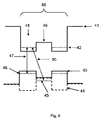
図9および10は、本発明の他の例を示したものである。この例は、井戸48および障壁49がいずれも総合「複合」量子井戸65中に存在する点を除き、図6に示されている好ましい例と同様である。この複合井戸65は、MQW構造中の単純な単一井戸層に取って代わることができるユニットを形成している1つまたは複数の井戸48および障壁49の一構造である。図10は、2つの他の障壁層67と隣接し、かつ、これらの障壁層67によって分離された3つのこのような複合量子井戸65の一例を示したものであるが、原理的には任意の数の複合量子井戸65および他の障壁67を使用することができる。井戸48と他の障壁67の間のエネルギー障壁差は、それぞれ伝導帯中および価電子帯中の井戸48と障壁49の間のエネルギー差より大きい。
9 and 10 show another example of the present invention. This example is similar to the preferred example shown in FIG. 6 except that the well 48 and the
このような構造には少なくとも3つの異なる材料組成が必要であり、そのうちの2つは、図9に示されている1つまたは複数の複合井戸65のための材料組成であり(1つは、1つまたは複数の井戸48のため、もう1つは、1つまたは複数の障壁49のため)、もう1つは、複合量子井戸間の1つまたは複数の他の障壁67のための材料組成である。この構造は、タイプ−Iおよびタイプ−IIの量子井戸の使用を介したTE利得およびTM利得に対する改良された制御に関して、図8で既に説明した構造の利点と同じ利点を有するが、ここでは、重い正孔間接遷移に対する電子の大きい重畳の設計に対する余分の自由が存在する。デバイスの設計者は、材料組成、個々の複合井戸中の井戸48および障壁49の厚さおよび相対数、他の障壁67の数と比較した複合井戸65の数、および他の障壁67の厚さおよび材料組成を変更することができる。1つまたは複数の他の障壁層67は、複合量子井戸65によって交互にはさまれていることが好ましい。「m」個の複合量子井戸65および「m±1」個の他の障壁層67が存在することが好ましい。さらに、利得媒体は、1つまたは複数の他の障壁層67によって分離された1つまたは複数の複合量子井戸65および1つまたは複数の標準単一量子井戸を備えることができる。
Such a structure requires at least three different material compositions, two of which are the material compositions for one or more
他の障壁67は、In1−x−yAlxGayAs(x>0、y>0)を含んでいることが好ましい。他の障壁67は、In1−x−yAlxGayAs(0<x<=0.48、0<y<0.6)を含んでいることが好ましい。他の障壁67は、無ひずみであることが好ましい。原理的には、複合量子井戸65は、1つまたは複数の井戸48および1つまたは複数の障壁49を有することができる。個々の複合量子井戸65中の個々の障壁49または井戸48は、異なる材料組成を使用して形成することができるが、製造を容易にするためには、複合量子井戸65中のすべての井戸48が同じ材料組成を有し、また、複合量子井戸65中のすべての障壁49が同じ材料組成を有することが望ましい。
The
1、12 上部電極
2、13 コンタクト層
3、14 p−型層
4 n−型ブロック層
5 p−型ブロック層
6 n−型クラッド層
7、18 n−型基板
8、19 下部電極
9 p−型キャップ層
10、17 利得媒体
11 n−型層
15、20 窒化ケイ素層
16 p−型クラッド層
21、27、33、51、59 電子バンド
22、34、42 第1の電子レベル
23、29、35 正孔バンド
24 第1の重い/軽い正孔レベル
25、39、48、57 井戸
26、32、67 障壁層
28 最小(第1の電子レベル)量子化電子エネルギー準位
30 最大量子化正孔エネルギー準位(第1の正孔レベル)
31 井戸層
36 第1の正孔波動関数
37 第1の正孔エネルギー準位
38 第1の電子波動関数(E波動関数)
40、49、58 障壁
41 電子帯端
43 軽い正孔帯端
44 重い正孔帯端
45 第1の重い正孔レベル
46 第1の軽い正孔レベル
47 電子−軽い正孔遷移
50 電子−重い正孔遷移
52 第1の(最小)電子エネルギー準位
53、61 重い正孔バンド
54 第1の重い正孔波動関数
55 第1の重い正孔エネルギー準位
56 電子波動関数
60 第1の重い正孔エネルギー準位波動関数
62 軽い正孔バンド
63 第1の軽い正孔エネルギー準位波動関数
64 第1の電子エネルギー準位波動関数
65 量子井戸(複合井戸、複合量子井戸)
DESCRIPTION OF
31
40, 49, 58
Claims (22)
A) 入射光を受け取り、かつ、増幅された光を射出するための光導波路と、
B) 光利得を提供するための隣接する複数の半導体層を備えた利得媒体と、
C) 前記利得媒体を通じて電流をポンプするための電極と
を備え、前記隣接する複数の半導体層が、電子のための1つまたは複数の量子井戸を画定し、かつ、前記利得媒体中における直接電子−正孔遷移および間接電子−正孔遷移の両方を提供するように動作し、それにより、
i) 伝導帯中の第1の量子化電子エネルギー準位が第1の層中に位置し、
ii) 価電子帯中の第1の量子化正孔エネルギー準位が前記第1の層中に位置し、
iii) 前記価電子帯中の他の第1の量子化正孔エネルギー準位が隣接する第2の層中に位置し、また、前記第2の層が前記第1の層とは異なる材料組成を有し、
前記第1の層中の前記第1の量子化正孔エネルギー準位が、軽い正孔状態か、あるいは重い正孔状態のいずれかであり、また、前記第2の層中の他の第1の量子化正孔エネルギー準位が、前記第1の層中の前記第1の量子化正孔エネルギー準位とは異なる正孔状態である光増幅器。 An optical amplifier for receiving incident light and emitting amplified light,
A) an optical waveguide for receiving incident light and emitting amplified light;
B) a gain medium with a plurality of adjacent semiconductor layers to provide optical gain;
C) an electrode for pumping current through the gain medium, wherein the adjacent semiconductor layers define one or more quantum wells for electrons and direct electrons in the gain medium Operate to provide both hole transitions and indirect electron-hole transitions, thereby
i) a first quantized electron energy level in the conduction band is located in the first layer;
ii) a first quantized hole energy level in the valence band is located in the first layer;
iii) Another first quantized hole energy level in the valence band is located in the adjacent second layer, and the second layer has a material composition different from that of the first layer. Have
The first quantized hole energy level in the first layer is either a light hole state or a heavy hole state, and the other first in the second layer The quantized hole energy level of the optical amplifier is a hole state different from the first quantized hole energy level in the first layer.
i) MC1と、前記第1の層の前記伝導帯中の前記第1の量子化電子エネルギー準位と前記第1の層の前記価電子帯中の前記第1の量子化正孔エネルギー準位の間の遷移からの利得との積が、
ii) MC2と、前記第1の層の前記伝導帯中の前記第1の量子化電子エネルギー準位と前記第2の層の前記価電子帯中の前記他の第1の量子化正孔エネルギー準位の間の遷移からの利得との積の
20%内で整合する、請求項1または2に記載の光増幅器。 The gain medium has a first mode confinement factor (MC1) for a first light polarization and a second mode confinement factor (MC2) for a second light polarization;
i) MC1, the first quantized electron energy level in the conduction band of the first layer, and the first quantized hole energy level in the valence band of the first layer. The product of the gain from the transition between is
ii) MC2, the first quantized electron energy level in the conduction band of the first layer, and the other first quantized hole energy in the valence band of the second layer. 3. An optical amplifier according to claim 1 or 2 that matches within 20% of the product of the gain from the transition between levels.
前記隣接する複数の半導体層が、電子のための1つまたは複数の量子井戸を画定し、かつ、前記利得媒体中における直接電子−正孔遷移および間接電子−正孔遷移の両方を提供するように動作し、それにより、
i) 伝導帯中の第1の量子化電子エネルギー準位が第1の層中に位置し、
ii) 価電子帯中の第1の量子化正孔エネルギー準位が前記第1の層中に位置し、
iii) 前記価電子帯中の他の第1の量子化正孔エネルギー準位が隣接する第2の層中に位置し、また、前記第2の層が前記第1の層とは異なる材料組成を有し、
前記第1の層中の前記第1の量子化正孔エネルギー準位が、軽い正孔状態か、あるいは重い正孔状態のいずれかであり、また、前記第2の層中の他の第1の量子化正孔エネルギー準位が、前記第1の層中の前記第1の量子化正孔エネルギー準位とは異なる正孔状態であり、また、
前記第2の層がIn1−x−yAlxGayAs(x>0、y>0)を含むデバイス。 A device comprising a gain medium, the gain medium comprising a plurality of adjacent semiconductor layers for providing optical gain;
The adjacent semiconductor layers define one or more quantum wells for electrons and provide both direct and indirect electron-hole transitions in the gain medium. And thereby
i) a first quantized electron energy level in the conduction band is located in the first layer;
ii) a first quantized hole energy level in the valence band is located in the first layer;
iii) Another first quantized hole energy level in the valence band is located in the adjacent second layer, and the second layer has a material composition different from that of the first layer. Have
The first quantized hole energy level in the first layer is either a light hole state or a heavy hole state, and the other first in the second layer The quantized hole energy level of the first layer is different from the first quantized hole energy level in the first layer, and
Wherein the second layer devices including In 1-x-y Al x Ga y As (x> 0, y> 0).
Applications Claiming Priority (3)
| Application Number | Priority Date | Filing Date | Title |
|---|---|---|---|
| GB1002391.9 | 2010-02-12 | ||
| GBGB1002391.9A GB201002391D0 (en) | 2010-02-12 | 2010-02-12 | Semiconductor device |
| PCT/GB2011/050255 WO2011098824A1 (en) | 2010-02-12 | 2011-02-11 | Semiconductor device |
Publications (2)
| Publication Number | Publication Date |
|---|---|
| JP2013520003A true JP2013520003A (en) | 2013-05-30 |
| JP5698267B2 JP5698267B2 (en) | 2015-04-08 |
Family
ID=42110625
Family Applications (1)
| Application Number | Title | Priority Date | Filing Date |
|---|---|---|---|
| JP2012552473A Active JP5698267B2 (en) | 2010-02-12 | 2011-02-11 | Semiconductor device |
Country Status (7)
| Country | Link |
|---|---|
| US (1) | US8687269B2 (en) |
| EP (1) | EP2526594B1 (en) |
| JP (1) | JP5698267B2 (en) |
| KR (1) | KR101404563B1 (en) |
| CN (1) | CN103119810B (en) |
| GB (1) | GB201002391D0 (en) |
| WO (1) | WO2011098824A1 (en) |
Cited By (2)
| Publication number | Priority date | Publication date | Assignee | Title |
|---|---|---|---|---|
| JP2015109365A (en) * | 2013-12-05 | 2015-06-11 | アンリツ株式会社 | Semiconductor optical amplifier |
| JP2017028330A (en) * | 2016-11-09 | 2017-02-02 | アンリツ株式会社 | Semiconductor optical amplifier |
Families Citing this family (4)
| Publication number | Priority date | Publication date | Assignee | Title |
|---|---|---|---|---|
| US9059356B1 (en) * | 2013-11-22 | 2015-06-16 | Sandia Corporation | Laterally injected light-emitting diode and laser diode |
| CN106233550B (en) * | 2014-02-28 | 2019-05-07 | 统雷量子电子有限公司 | Passive waveguide structure for opto-electronic device |
| JP6325948B2 (en) | 2014-09-02 | 2018-05-16 | 株式会社東芝 | Semiconductor light emitting device and optical coupling device |
| CN106154413B (en) * | 2015-04-21 | 2019-08-02 | 中国科学院苏州纳米技术与纳米仿生研究所 | Optical waveguide |
Citations (1)
| Publication number | Priority date | Publication date | Assignee | Title |
|---|---|---|---|---|
| JP2009224691A (en) * | 2008-03-18 | 2009-10-01 | Fujitsu Ltd | Semiconductor optical amplifier, its manufacturing process, and semiconductor optical integrated element |
Family Cites Families (4)
| Publication number | Priority date | Publication date | Assignee | Title |
|---|---|---|---|---|
| GB9620966D0 (en) * | 1996-10-08 | 1996-11-27 | Ncr Int Inc | Magnetic card sensor |
| JP2001053392A (en) | 1999-06-03 | 2001-02-23 | Fujitsu Ltd | Polarization-independent type semiconductor optical amplifier |
| KR100602973B1 (en) * | 2003-10-30 | 2006-07-20 | 한국과학기술연구원 | Single mode laser diode using strain compensated multi-quantum-wells and method for manufacturing the same |
| JP4584079B2 (en) | 2005-08-31 | 2010-11-17 | 富士通株式会社 | Semiconductor optical amplifier and optical integrated circuit |
-
2010
- 2010-02-12 GB GBGB1002391.9A patent/GB201002391D0/en not_active Ceased
-
2011
- 2011-02-11 CN CN201180016780.3A patent/CN103119810B/en active Active
- 2011-02-11 JP JP2012552473A patent/JP5698267B2/en active Active
- 2011-02-11 EP EP11703928.9A patent/EP2526594B1/en active Active
- 2011-02-11 WO PCT/GB2011/050255 patent/WO2011098824A1/en active Application Filing
- 2011-02-11 KR KR1020127022577A patent/KR101404563B1/en active IP Right Grant
-
2012
- 2012-08-10 US US13/572,587 patent/US8687269B2/en active Active
Patent Citations (1)
| Publication number | Priority date | Publication date | Assignee | Title |
|---|---|---|---|---|
| JP2009224691A (en) * | 2008-03-18 | 2009-10-01 | Fujitsu Ltd | Semiconductor optical amplifier, its manufacturing process, and semiconductor optical integrated element |
Non-Patent Citations (1)
| Title |
|---|
| JPN6015002616; IEEE Journal of Electronics Vol.34,No.12, 199812, 2340-2349 * |
Cited By (2)
| Publication number | Priority date | Publication date | Assignee | Title |
|---|---|---|---|---|
| JP2015109365A (en) * | 2013-12-05 | 2015-06-11 | アンリツ株式会社 | Semiconductor optical amplifier |
| JP2017028330A (en) * | 2016-11-09 | 2017-02-02 | アンリツ株式会社 | Semiconductor optical amplifier |
Also Published As
| Publication number | Publication date |
|---|---|
| KR101404563B1 (en) | 2014-06-09 |
| US8687269B2 (en) | 2014-04-01 |
| KR20120123116A (en) | 2012-11-07 |
| EP2526594B1 (en) | 2015-06-17 |
| JP5698267B2 (en) | 2015-04-08 |
| GB201002391D0 (en) | 2010-03-31 |
| CN103119810B (en) | 2015-11-25 |
| US20130033743A1 (en) | 2013-02-07 |
| CN103119810A (en) | 2013-05-22 |
| EP2526594A1 (en) | 2012-11-28 |
| WO2011098824A1 (en) | 2011-08-18 |
Similar Documents
| Publication | Publication Date | Title |
|---|---|---|
| JP3854560B2 (en) | Quantum optical semiconductor device | |
| CN104011950B (en) | High-density laser device optics | |
| US20080291952A1 (en) | Optical semiconductor device | |
| Sweeney et al. | Optoelectronic devices and materials | |
| EP0390167B1 (en) | Semiconductor laser device having plurality of layers for emitting lights of different wavelengths and method of driving the same | |
| US6252895B1 (en) | Distributed feedback semiconductor laser in which light intensity distributions differ in different polarization modes, and driving method therefor | |
| JP5698267B2 (en) | Semiconductor device | |
| US5289484A (en) | Laser diode | |
| JP2009076942A (en) | Distributed-feedback semiconductor laser, distributed-feedback semiconductor laser array, and optical module | |
| JP2005538532A (en) | Tilted cavity semiconductor laser (TCSL) and manufacturing method thereof | |
| JPH118442A (en) | Optical semiconductor device, optical communication system provided therewith, and method therefor | |
| JP2003202529A (en) | Semiconductor optical modulator, semiconductor light emitting device and wavelength variable laser device and multiwavelength laser device and optical transmission system | |
| WO2001029943A1 (en) | Method and apparatus for long wavelength semiconductor lasers | |
| EP1760851B1 (en) | Semiconductor optical amplification device and optical integrated circuit | |
| US7949020B2 (en) | Semiconductor laser and optical integrated semiconductor device | |
| CN105830292A (en) | Semiconductor laser array, semiconductor laser element, semiconductor laser module, and wavelength-variable laser assembly | |
| JPH04783A (en) | Semiconductor optical element | |
| JP2009260093A (en) | Optical semiconductor device | |
| JP2004179206A (en) | Optical semiconductor device, optical transmission module and optical amplification module | |
| JP2007219561A (en) | Semiconductor light emitting device | |
| EP1505699B1 (en) | Semiconductor optical device on an indium phosphide substrate for long operating wavelengths | |
| US7852897B2 (en) | Semiconductor laser optical integrated semiconductor device | |
| JP4999038B2 (en) | Manufacturing method of semiconductor device | |
| JPH0529716A (en) | Optical semiconductor element | |
| JP5057477B2 (en) | Semiconductor laser element |
Legal Events
| Date | Code | Title | Description |
|---|---|---|---|
| A977 | Report on retrieval |
Free format text: JAPANESE INTERMEDIATE CODE: A971007 Effective date: 20130927 |
|
| A131 | Notification of reasons for refusal |
Free format text: JAPANESE INTERMEDIATE CODE: A131 Effective date: 20131008 |
|
| A521 | Request for written amendment filed |
Free format text: JAPANESE INTERMEDIATE CODE: A523 Effective date: 20140107 |
|
| A02 | Decision of refusal |
Free format text: JAPANESE INTERMEDIATE CODE: A02 Effective date: 20140714 |
|
| A521 | Request for written amendment filed |
Free format text: JAPANESE INTERMEDIATE CODE: A523 Effective date: 20141112 |
|
| A911 | Transfer to examiner for re-examination before appeal (zenchi) |
Free format text: JAPANESE INTERMEDIATE CODE: A911 Effective date: 20141120 |
|
| TRDD | Decision of grant or rejection written | ||
| A01 | Written decision to grant a patent or to grant a registration (utility model) |
Free format text: JAPANESE INTERMEDIATE CODE: A01 Effective date: 20150126 |
|
| A61 | First payment of annual fees (during grant procedure) |
Free format text: JAPANESE INTERMEDIATE CODE: A61 Effective date: 20150212 |
|
| R150 | Certificate of patent or registration of utility model |
Ref document number: 5698267 Country of ref document: JP Free format text: JAPANESE INTERMEDIATE CODE: R150 |
|
| S111 | Request for change of ownership or part of ownership |
Free format text: JAPANESE INTERMEDIATE CODE: R313113 |
|
| R350 | Written notification of registration of transfer |
Free format text: JAPANESE INTERMEDIATE CODE: R350 |
|
| R250 | Receipt of annual fees |
Free format text: JAPANESE INTERMEDIATE CODE: R250 |
|
| R250 | Receipt of annual fees |
Free format text: JAPANESE INTERMEDIATE CODE: R250 |
|
| R250 | Receipt of annual fees |
Free format text: JAPANESE INTERMEDIATE CODE: R250 |
|
| R250 | Receipt of annual fees |
Free format text: JAPANESE INTERMEDIATE CODE: R250 |
|
| R250 | Receipt of annual fees |
Free format text: JAPANESE INTERMEDIATE CODE: R250 |
|
| R250 | Receipt of annual fees |
Free format text: JAPANESE INTERMEDIATE CODE: R250 |
|
| R250 | Receipt of annual fees |
Free format text: JAPANESE INTERMEDIATE CODE: R250 |