JP2013510397A - Multilayer metal electrodes for optoelectronic devices - Google Patents
Multilayer metal electrodes for optoelectronic devices Download PDFInfo
- Publication number
- JP2013510397A JP2013510397A JP2012537367A JP2012537367A JP2013510397A JP 2013510397 A JP2013510397 A JP 2013510397A JP 2012537367 A JP2012537367 A JP 2012537367A JP 2012537367 A JP2012537367 A JP 2012537367A JP 2013510397 A JP2013510397 A JP 2013510397A
- Authority
- JP
- Japan
- Prior art keywords
- electrode
- film
- oxide
- metal film
- electrode according
- Prior art date
- Legal status (The legal status is an assumption and is not a legal conclusion. Google has not performed a legal analysis and makes no representation as to the accuracy of the status listed.)
- Withdrawn
Links
- 229910052751 metal Inorganic materials 0.000 title claims abstract description 48
- 239000002184 metal Substances 0.000 title claims abstract description 48
- 230000005693 optoelectronics Effects 0.000 title claims abstract description 10
- 239000000463 material Substances 0.000 claims abstract description 25
- 239000000758 substrate Substances 0.000 claims abstract description 22
- 229910052782 aluminium Inorganic materials 0.000 claims abstract description 15
- 229910052737 gold Inorganic materials 0.000 claims abstract description 13
- 229910052709 silver Inorganic materials 0.000 claims abstract description 13
- 229910052759 nickel Inorganic materials 0.000 claims abstract description 12
- 239000000203 mixture Substances 0.000 claims abstract description 11
- 229910052719 titanium Inorganic materials 0.000 claims abstract description 11
- 229910052804 chromium Inorganic materials 0.000 claims abstract description 9
- 229910052802 copper Inorganic materials 0.000 claims abstract description 9
- 229910052697 platinum Inorganic materials 0.000 claims abstract description 8
- 239000010408 film Substances 0.000 claims description 135
- 239000010949 copper Substances 0.000 claims description 79
- PXHVJJICTQNCMI-UHFFFAOYSA-N nickel Substances [Ni] PXHVJJICTQNCMI-UHFFFAOYSA-N 0.000 claims description 28
- 239000010936 titanium Substances 0.000 claims description 28
- XLOMVQKBTHCTTD-UHFFFAOYSA-N Zinc monoxide Chemical compound [Zn]=O XLOMVQKBTHCTTD-UHFFFAOYSA-N 0.000 claims description 24
- 239000010931 gold Substances 0.000 claims description 12
- 239000011787 zinc oxide Substances 0.000 claims description 12
- 239000012528 membrane Substances 0.000 claims description 11
- BASFCYQUMIYNBI-UHFFFAOYSA-N platinum Substances [Pt] BASFCYQUMIYNBI-UHFFFAOYSA-N 0.000 claims description 9
- 239000011651 chromium Substances 0.000 claims description 8
- 239000012298 atmosphere Substances 0.000 claims description 6
- 239000010944 silver (metal) Substances 0.000 claims description 6
- XOLBLPGZBRYERU-UHFFFAOYSA-N tin dioxide Chemical compound O=[Sn]=O XOLBLPGZBRYERU-UHFFFAOYSA-N 0.000 claims description 6
- GWEVSGVZZGPLCZ-UHFFFAOYSA-N Titan oxide Chemical compound O=[Ti]=O GWEVSGVZZGPLCZ-UHFFFAOYSA-N 0.000 claims description 4
- 229910052791 calcium Inorganic materials 0.000 claims description 4
- 239000011575 calcium Substances 0.000 claims description 4
- 229910052738 indium Inorganic materials 0.000 claims description 4
- 229910052749 magnesium Inorganic materials 0.000 claims description 4
- 239000011777 magnesium Substances 0.000 claims description 4
- 229910052718 tin Inorganic materials 0.000 claims description 4
- 229910001887 tin oxide Inorganic materials 0.000 claims description 4
- OGIDPMRJRNCKJF-UHFFFAOYSA-N titanium oxide Inorganic materials [Ti]=O OGIDPMRJRNCKJF-UHFFFAOYSA-N 0.000 claims description 4
- 229910052725 zinc Inorganic materials 0.000 claims description 4
- 239000011701 zinc Substances 0.000 claims description 4
- QPLDLSVMHZLSFG-UHFFFAOYSA-N Copper oxide Chemical compound [Cu]=O QPLDLSVMHZLSFG-UHFFFAOYSA-N 0.000 claims description 2
- 239000005751 Copper oxide Substances 0.000 claims description 2
- WGLPBDUCMAPZCE-UHFFFAOYSA-N Trioxochromium Chemical compound O=[Cr](=O)=O WGLPBDUCMAPZCE-UHFFFAOYSA-N 0.000 claims description 2
- BRPQOXSCLDDYGP-UHFFFAOYSA-N calcium oxide Chemical compound [O-2].[Ca+2] BRPQOXSCLDDYGP-UHFFFAOYSA-N 0.000 claims description 2
- ODINCKMPIJJUCX-UHFFFAOYSA-N calcium oxide Inorganic materials [Ca]=O ODINCKMPIJJUCX-UHFFFAOYSA-N 0.000 claims description 2
- 239000000292 calcium oxide Substances 0.000 claims description 2
- 229910000423 chromium oxide Inorganic materials 0.000 claims description 2
- 229910000431 copper oxide Inorganic materials 0.000 claims description 2
- 229910052733 gallium Inorganic materials 0.000 claims description 2
- 229910003437 indium oxide Inorganic materials 0.000 claims description 2
- PJXISJQVUVHSOJ-UHFFFAOYSA-N indium(iii) oxide Chemical compound [O-2].[O-2].[O-2].[In+3].[In+3] PJXISJQVUVHSOJ-UHFFFAOYSA-N 0.000 claims description 2
- CPLXHLVBOLITMK-UHFFFAOYSA-N magnesium oxide Inorganic materials [Mg]=O CPLXHLVBOLITMK-UHFFFAOYSA-N 0.000 claims description 2
- 239000000395 magnesium oxide Substances 0.000 claims description 2
- AXZKOIWUVFPNLO-UHFFFAOYSA-N magnesium;oxygen(2-) Chemical compound [O-2].[Mg+2] AXZKOIWUVFPNLO-UHFFFAOYSA-N 0.000 claims description 2
- 229910000480 nickel oxide Inorganic materials 0.000 claims description 2
- 229910052758 niobium Inorganic materials 0.000 claims description 2
- TWNQGVIAIRXVLR-UHFFFAOYSA-N oxo(oxoalumanyloxy)alumane Chemical compound O=[Al]O[Al]=O TWNQGVIAIRXVLR-UHFFFAOYSA-N 0.000 claims description 2
- GNRSAWUEBMWBQH-UHFFFAOYSA-N oxonickel Chemical compound [Ni]=O GNRSAWUEBMWBQH-UHFFFAOYSA-N 0.000 claims description 2
- 229910052715 tantalum Inorganic materials 0.000 claims description 2
- 239000010409 thin film Substances 0.000 claims 1
- 238000002834 transmittance Methods 0.000 abstract description 28
- 239000010410 layer Substances 0.000 description 20
- 238000000151 deposition Methods 0.000 description 19
- 230000008021 deposition Effects 0.000 description 16
- 238000000137 annealing Methods 0.000 description 10
- 230000003287 optical effect Effects 0.000 description 10
- 239000000523 sample Substances 0.000 description 10
- OKTJSMMVPCPJKN-UHFFFAOYSA-N Carbon Chemical compound [C] OKTJSMMVPCPJKN-UHFFFAOYSA-N 0.000 description 8
- 239000004020 conductor Substances 0.000 description 8
- 230000003647 oxidation Effects 0.000 description 7
- 238000007254 oxidation reaction Methods 0.000 description 7
- 238000004544 sputter deposition Methods 0.000 description 7
- 230000005540 biological transmission Effects 0.000 description 5
- 238000010438 heat treatment Methods 0.000 description 5
- 238000000034 method Methods 0.000 description 5
- 239000002109 single walled nanotube Substances 0.000 description 5
- 239000011149 active material Substances 0.000 description 4
- 238000004630 atomic force microscopy Methods 0.000 description 4
- 229910021389 graphene Inorganic materials 0.000 description 4
- 238000004519 manufacturing process Methods 0.000 description 4
- 230000035515 penetration Effects 0.000 description 4
- 239000004065 semiconductor Substances 0.000 description 4
- VYPSYNLAJGMNEJ-UHFFFAOYSA-N Silicium dioxide Chemical compound O=[Si]=O VYPSYNLAJGMNEJ-UHFFFAOYSA-N 0.000 description 3
- 230000006399 behavior Effects 0.000 description 3
- 238000005516 engineering process Methods 0.000 description 3
- AMGQUBHHOARCQH-UHFFFAOYSA-N indium;oxotin Chemical compound [In].[Sn]=O AMGQUBHHOARCQH-UHFFFAOYSA-N 0.000 description 3
- 230000003746 surface roughness Effects 0.000 description 3
- 238000000411 transmission spectrum Methods 0.000 description 3
- CSCPPACGZOOCGX-UHFFFAOYSA-N Acetone Chemical compound CC(C)=O CSCPPACGZOOCGX-UHFFFAOYSA-N 0.000 description 2
- XKRFYHLGVUSROY-UHFFFAOYSA-N Argon Chemical compound [Ar] XKRFYHLGVUSROY-UHFFFAOYSA-N 0.000 description 2
- IJGRMHOSHXDMSA-UHFFFAOYSA-N Atomic nitrogen Chemical compound N#N IJGRMHOSHXDMSA-UHFFFAOYSA-N 0.000 description 2
- OYPRJOBELJOOCE-UHFFFAOYSA-N Calcium Chemical compound [Ca] OYPRJOBELJOOCE-UHFFFAOYSA-N 0.000 description 2
- VYZAMTAEIAYCRO-UHFFFAOYSA-N Chromium Chemical compound [Cr] VYZAMTAEIAYCRO-UHFFFAOYSA-N 0.000 description 2
- LFQSCWFLJHTTHZ-UHFFFAOYSA-N Ethanol Chemical compound CCO LFQSCWFLJHTTHZ-UHFFFAOYSA-N 0.000 description 2
- 229910003327 LiNbO3 Inorganic materials 0.000 description 2
- FYYHWMGAXLPEAU-UHFFFAOYSA-N Magnesium Chemical compound [Mg] FYYHWMGAXLPEAU-UHFFFAOYSA-N 0.000 description 2
- BQCADISMDOOEFD-UHFFFAOYSA-N Silver Chemical compound [Ag] BQCADISMDOOEFD-UHFFFAOYSA-N 0.000 description 2
- ATJFFYVFTNAWJD-UHFFFAOYSA-N Tin Chemical compound [Sn] ATJFFYVFTNAWJD-UHFFFAOYSA-N 0.000 description 2
- RTAQQCXQSZGOHL-UHFFFAOYSA-N Titanium Chemical compound [Ti] RTAQQCXQSZGOHL-UHFFFAOYSA-N 0.000 description 2
- HCHKCACWOHOZIP-UHFFFAOYSA-N Zinc Chemical compound [Zn] HCHKCACWOHOZIP-UHFFFAOYSA-N 0.000 description 2
- 238000010521 absorption reaction Methods 0.000 description 2
- XAGFODPZIPBFFR-UHFFFAOYSA-N aluminium Chemical compound [Al] XAGFODPZIPBFFR-UHFFFAOYSA-N 0.000 description 2
- 239000012080 ambient air Substances 0.000 description 2
- 238000004458 analytical method Methods 0.000 description 2
- QVGXLLKOCUKJST-UHFFFAOYSA-N atomic oxygen Chemical compound [O] QVGXLLKOCUKJST-UHFFFAOYSA-N 0.000 description 2
- 230000008033 biological extinction Effects 0.000 description 2
- 238000010586 diagram Methods 0.000 description 2
- 238000009792 diffusion process Methods 0.000 description 2
- 238000005401 electroluminescence Methods 0.000 description 2
- PCHJSUWPFVWCPO-UHFFFAOYSA-N gold Chemical compound [Au] PCHJSUWPFVWCPO-UHFFFAOYSA-N 0.000 description 2
- 238000011065 in-situ storage Methods 0.000 description 2
- APFVFJFRJDLVQX-UHFFFAOYSA-N indium atom Chemical compound [In] APFVFJFRJDLVQX-UHFFFAOYSA-N 0.000 description 2
- 150000002739 metals Chemical class 0.000 description 2
- 239000011368 organic material Substances 0.000 description 2
- 239000001301 oxygen Substances 0.000 description 2
- 229910052760 oxygen Inorganic materials 0.000 description 2
- 230000000737 periodic effect Effects 0.000 description 2
- 229920000139 polyethylene terephthalate Polymers 0.000 description 2
- 239000005020 polyethylene terephthalate Substances 0.000 description 2
- 238000002310 reflectometry Methods 0.000 description 2
- 239000004332 silver Substances 0.000 description 2
- 238000001228 spectrum Methods 0.000 description 2
- ZOXJGFHDIHLPTG-UHFFFAOYSA-N Boron Chemical compound [B] ZOXJGFHDIHLPTG-UHFFFAOYSA-N 0.000 description 1
- 229910002482 Cu–Ni Inorganic materials 0.000 description 1
- 229910017945 Cu—Ti Inorganic materials 0.000 description 1
- 229910013641 LiNbO 3 Inorganic materials 0.000 description 1
- BPQQTUXANYXVAA-UHFFFAOYSA-N Orthosilicate Chemical compound [O-][Si]([O-])([O-])[O-] BPQQTUXANYXVAA-UHFFFAOYSA-N 0.000 description 1
- XUIMIQQOPSSXEZ-UHFFFAOYSA-N Silicon Chemical compound [Si] XUIMIQQOPSSXEZ-UHFFFAOYSA-N 0.000 description 1
- 229910010413 TiO 2 Inorganic materials 0.000 description 1
- 229910052786 argon Inorganic materials 0.000 description 1
- 239000012300 argon atmosphere Substances 0.000 description 1
- 230000015572 biosynthetic process Effects 0.000 description 1
- 229910052796 boron Inorganic materials 0.000 description 1
- 239000013590 bulk material Substances 0.000 description 1
- 239000002041 carbon nanotube Substances 0.000 description 1
- 229910021393 carbon nanotube Inorganic materials 0.000 description 1
- 239000011248 coating agent Substances 0.000 description 1
- 238000000576 coating method Methods 0.000 description 1
- 230000007797 corrosion Effects 0.000 description 1
- 238000005260 corrosion Methods 0.000 description 1
- 239000013078 crystal Substances 0.000 description 1
- 230000007812 deficiency Effects 0.000 description 1
- 230000001419 dependent effect Effects 0.000 description 1
- 239000003989 dielectric material Substances 0.000 description 1
- 230000005611 electricity Effects 0.000 description 1
- 238000009713 electroplating Methods 0.000 description 1
- 230000007613 environmental effect Effects 0.000 description 1
- 230000001747 exhibiting effect Effects 0.000 description 1
- 229920002457 flexible plastic Polymers 0.000 description 1
- 239000005350 fused silica glass Substances 0.000 description 1
- 239000011521 glass Substances 0.000 description 1
- 239000007788 liquid Substances 0.000 description 1
- 239000004973 liquid crystal related substance Substances 0.000 description 1
- GQYHUHYESMUTHG-UHFFFAOYSA-N lithium niobate Chemical compound [Li+].[O-][Nb](=O)=O GQYHUHYESMUTHG-UHFFFAOYSA-N 0.000 description 1
- 238000001459 lithography Methods 0.000 description 1
- 238000001755 magnetron sputter deposition Methods 0.000 description 1
- 238000004377 microelectronic Methods 0.000 description 1
- 239000002070 nanowire Substances 0.000 description 1
- 229910052757 nitrogen Inorganic materials 0.000 description 1
- 239000012044 organic layer Substances 0.000 description 1
- 230000001590 oxidative effect Effects 0.000 description 1
- 238000002161 passivation Methods 0.000 description 1
- 238000005325 percolation Methods 0.000 description 1
- 239000011112 polyethylene naphthalate Substances 0.000 description 1
- -1 polyethylene terephthalate Polymers 0.000 description 1
- 230000001681 protective effect Effects 0.000 description 1
- 239000010453 quartz Substances 0.000 description 1
- 238000007650 screen-printing Methods 0.000 description 1
- 229910052710 silicon Inorganic materials 0.000 description 1
- 239000010703 silicon Substances 0.000 description 1
- 230000005476 size effect Effects 0.000 description 1
- 238000002174 soft lithography Methods 0.000 description 1
- 239000007787 solid Substances 0.000 description 1
- 239000000126 substance Substances 0.000 description 1
- 238000006467 substitution reaction Methods 0.000 description 1
- 238000007740 vapor deposition Methods 0.000 description 1
Images


Classifications
-
- H—ELECTRICITY
- H01—ELECTRIC ELEMENTS
- H01L—SEMICONDUCTOR DEVICES NOT COVERED BY CLASS H10
- H01L31/00—Semiconductor devices sensitive to infrared radiation, light, electromagnetic radiation of shorter wavelength or corpuscular radiation and specially adapted either for the conversion of the energy of such radiation into electrical energy or for the control of electrical energy by such radiation; Processes or apparatus specially adapted for the manufacture or treatment thereof or of parts thereof; Details thereof
- H01L31/02—Details
- H01L31/0224—Electrodes
- H01L31/022466—Electrodes made of transparent conductive layers, e.g. TCO, ITO layers
-
- B—PERFORMING OPERATIONS; TRANSPORTING
- B82—NANOTECHNOLOGY
- B82Y—SPECIFIC USES OR APPLICATIONS OF NANOSTRUCTURES; MEASUREMENT OR ANALYSIS OF NANOSTRUCTURES; MANUFACTURE OR TREATMENT OF NANOSTRUCTURES
- B82Y10/00—Nanotechnology for information processing, storage or transmission, e.g. quantum computing or single electron logic
-
- G—PHYSICS
- G02—OPTICS
- G02F—OPTICAL DEVICES OR ARRANGEMENTS FOR THE CONTROL OF LIGHT BY MODIFICATION OF THE OPTICAL PROPERTIES OF THE MEDIA OF THE ELEMENTS INVOLVED THEREIN; NON-LINEAR OPTICS; FREQUENCY-CHANGING OF LIGHT; OPTICAL LOGIC ELEMENTS; OPTICAL ANALOGUE/DIGITAL CONVERTERS
- G02F1/00—Devices or arrangements for the control of the intensity, colour, phase, polarisation or direction of light arriving from an independent light source, e.g. switching, gating or modulating; Non-linear optics
- G02F1/01—Devices or arrangements for the control of the intensity, colour, phase, polarisation or direction of light arriving from an independent light source, e.g. switching, gating or modulating; Non-linear optics for the control of the intensity, phase, polarisation or colour
- G02F1/13—Devices or arrangements for the control of the intensity, colour, phase, polarisation or direction of light arriving from an independent light source, e.g. switching, gating or modulating; Non-linear optics for the control of the intensity, phase, polarisation or colour based on liquid crystals, e.g. single liquid crystal display cells
- G02F1/133—Constructional arrangements; Operation of liquid crystal cells; Circuit arrangements
- G02F1/1333—Constructional arrangements; Manufacturing methods
- G02F1/1343—Electrodes
- G02F1/13439—Electrodes characterised by their electrical, optical, physical properties; materials therefor; method of making
-
- H—ELECTRICITY
- H01—ELECTRIC ELEMENTS
- H01G—CAPACITORS; CAPACITORS, RECTIFIERS, DETECTORS, SWITCHING DEVICES OR LIGHT-SENSITIVE DEVICES, OF THE ELECTROLYTIC TYPE
- H01G9/00—Electrolytic capacitors, rectifiers, detectors, switching devices, light-sensitive or temperature-sensitive devices; Processes of their manufacture
- H01G9/20—Light-sensitive devices
- H01G9/2027—Light-sensitive devices comprising an oxide semiconductor electrode
- H01G9/2031—Light-sensitive devices comprising an oxide semiconductor electrode comprising titanium oxide, e.g. TiO2
-
- H—ELECTRICITY
- H01—ELECTRIC ELEMENTS
- H01L—SEMICONDUCTOR DEVICES NOT COVERED BY CLASS H10
- H01L31/00—Semiconductor devices sensitive to infrared radiation, light, electromagnetic radiation of shorter wavelength or corpuscular radiation and specially adapted either for the conversion of the energy of such radiation into electrical energy or for the control of electrical energy by such radiation; Processes or apparatus specially adapted for the manufacture or treatment thereof or of parts thereof; Details thereof
- H01L31/18—Processes or apparatus specially adapted for the manufacture or treatment of these devices or of parts thereof
- H01L31/1884—Manufacture of transparent electrodes, e.g. TCO, ITO
-
- H—ELECTRICITY
- H01—ELECTRIC ELEMENTS
- H01L—SEMICONDUCTOR DEVICES NOT COVERED BY CLASS H10
- H01L33/00—Semiconductor devices with at least one potential-jump barrier or surface barrier specially adapted for light emission; Processes or apparatus specially adapted for the manufacture or treatment thereof or of parts thereof; Details thereof
- H01L33/36—Semiconductor devices with at least one potential-jump barrier or surface barrier specially adapted for light emission; Processes or apparatus specially adapted for the manufacture or treatment thereof or of parts thereof; Details thereof characterised by the electrodes
- H01L33/40—Materials therefor
- H01L33/42—Transparent materials
-
- H—ELECTRICITY
- H05—ELECTRIC TECHNIQUES NOT OTHERWISE PROVIDED FOR
- H05B—ELECTRIC HEATING; ELECTRIC LIGHT SOURCES NOT OTHERWISE PROVIDED FOR; CIRCUIT ARRANGEMENTS FOR ELECTRIC LIGHT SOURCES, IN GENERAL
- H05B33/00—Electroluminescent light sources
- H05B33/12—Light sources with substantially two-dimensional radiating surfaces
- H05B33/26—Light sources with substantially two-dimensional radiating surfaces characterised by the composition or arrangement of the conductive material used as an electrode
- H05B33/28—Light sources with substantially two-dimensional radiating surfaces characterised by the composition or arrangement of the conductive material used as an electrode of translucent electrodes
-
- H—ELECTRICITY
- H10—SEMICONDUCTOR DEVICES; ELECTRIC SOLID-STATE DEVICES NOT OTHERWISE PROVIDED FOR
- H10K—ORGANIC ELECTRIC SOLID-STATE DEVICES
- H10K30/00—Organic devices sensitive to infrared radiation, light, electromagnetic radiation of shorter wavelength or corpuscular radiation
- H10K30/80—Constructional details
- H10K30/81—Electrodes
- H10K30/82—Transparent electrodes, e.g. indium tin oxide [ITO] electrodes
-
- H—ELECTRICITY
- H10—SEMICONDUCTOR DEVICES; ELECTRIC SOLID-STATE DEVICES NOT OTHERWISE PROVIDED FOR
- H10K—ORGANIC ELECTRIC SOLID-STATE DEVICES
- H10K50/00—Organic light-emitting devices
- H10K50/80—Constructional details
- H10K50/805—Electrodes
- H10K50/82—Cathodes
- H10K50/828—Transparent cathodes, e.g. comprising thin metal layers
-
- G—PHYSICS
- G21—NUCLEAR PHYSICS; NUCLEAR ENGINEERING
- G21K—TECHNIQUES FOR HANDLING PARTICLES OR IONISING RADIATION NOT OTHERWISE PROVIDED FOR; IRRADIATION DEVICES; GAMMA RAY OR X-RAY MICROSCOPES
- G21K2201/00—Arrangements for handling radiation or particles
- G21K2201/06—Arrangements for handling radiation or particles using diffractive, refractive or reflecting elements
- G21K2201/061—Arrangements for handling radiation or particles using diffractive, refractive or reflecting elements characterised by a multilayer structure
-
- H—ELECTRICITY
- H01—ELECTRIC ELEMENTS
- H01J—ELECTRIC DISCHARGE TUBES OR DISCHARGE LAMPS
- H01J2211/00—Plasma display panels with alternate current induction of the discharge, e.g. AC-PDPs
- H01J2211/20—Constructional details
- H01J2211/22—Electrodes
- H01J2211/225—Material of electrodes
-
- H—ELECTRICITY
- H01—ELECTRIC ELEMENTS
- H01L—SEMICONDUCTOR DEVICES NOT COVERED BY CLASS H10
- H01L33/00—Semiconductor devices with at least one potential-jump barrier or surface barrier specially adapted for light emission; Processes or apparatus specially adapted for the manufacture or treatment thereof or of parts thereof; Details thereof
- H01L33/36—Semiconductor devices with at least one potential-jump barrier or surface barrier specially adapted for light emission; Processes or apparatus specially adapted for the manufacture or treatment thereof or of parts thereof; Details thereof characterised by the electrodes
- H01L33/40—Materials therefor
- H01L33/405—Reflective materials
-
- H—ELECTRICITY
- H10—SEMICONDUCTOR DEVICES; ELECTRIC SOLID-STATE DEVICES NOT OTHERWISE PROVIDED FOR
- H10K—ORGANIC ELECTRIC SOLID-STATE DEVICES
- H10K50/00—Organic light-emitting devices
- H10K50/80—Constructional details
- H10K50/805—Electrodes
- H10K50/81—Anodes
- H10K50/816—Multilayers, e.g. transparent multilayers
-
- Y—GENERAL TAGGING OF NEW TECHNOLOGICAL DEVELOPMENTS; GENERAL TAGGING OF CROSS-SECTIONAL TECHNOLOGIES SPANNING OVER SEVERAL SECTIONS OF THE IPC; TECHNICAL SUBJECTS COVERED BY FORMER USPC CROSS-REFERENCE ART COLLECTIONS [XRACs] AND DIGESTS
- Y02—TECHNOLOGIES OR APPLICATIONS FOR MITIGATION OR ADAPTATION AGAINST CLIMATE CHANGE
- Y02E—REDUCTION OF GREENHOUSE GAS [GHG] EMISSIONS, RELATED TO ENERGY GENERATION, TRANSMISSION OR DISTRIBUTION
- Y02E10/00—Energy generation through renewable energy sources
- Y02E10/50—Photovoltaic [PV] energy
- Y02E10/542—Dye sensitized solar cells
-
- Y—GENERAL TAGGING OF NEW TECHNOLOGICAL DEVELOPMENTS; GENERAL TAGGING OF CROSS-SECTIONAL TECHNOLOGIES SPANNING OVER SEVERAL SECTIONS OF THE IPC; TECHNICAL SUBJECTS COVERED BY FORMER USPC CROSS-REFERENCE ART COLLECTIONS [XRACs] AND DIGESTS
- Y02—TECHNOLOGIES OR APPLICATIONS FOR MITIGATION OR ADAPTATION AGAINST CLIMATE CHANGE
- Y02E—REDUCTION OF GREENHOUSE GAS [GHG] EMISSIONS, RELATED TO ENERGY GENERATION, TRANSMISSION OR DISTRIBUTION
- Y02E10/00—Energy generation through renewable energy sources
- Y02E10/50—Photovoltaic [PV] energy
- Y02E10/549—Organic PV cells
Landscapes
- Physics & Mathematics (AREA)
- Engineering & Computer Science (AREA)
- Power Engineering (AREA)
- Microelectronics & Electronic Packaging (AREA)
- Electromagnetism (AREA)
- General Physics & Mathematics (AREA)
- Chemical & Material Sciences (AREA)
- Computer Hardware Design (AREA)
- Optics & Photonics (AREA)
- Nonlinear Science (AREA)
- Mathematical Physics (AREA)
- Condensed Matter Physics & Semiconductors (AREA)
- Crystallography & Structural Chemistry (AREA)
- Nanotechnology (AREA)
- Manufacturing & Machinery (AREA)
- Theoretical Computer Science (AREA)
- Non-Insulated Conductors (AREA)
- Electroluminescent Light Sources (AREA)
- Physical Vapour Deposition (AREA)
- Electrodes Of Semiconductors (AREA)
- Photovoltaic Devices (AREA)
Abstract
本発明は、基板(1)と、少なくとも1つの極薄金属膜(3)と接触する導電膜(2)からなる層状構造部と、を備え、2つの膜(2,3)が異なる材料からなり、前記導電膜(2)がCu、Au、Ag、Alから選択され、前記極薄金属膜(3)がNi、Cr、Ti、Pt、Ag、Au、Alおよびこれらの混合物から選択される電極に関する。電極は、光電子デバイスに特に有益であり、良好な導電率、透過率および安定性を示す。 The present invention comprises a substrate (1) and a layered structure made of a conductive film (2) in contact with at least one ultrathin metal film (3), and the two films (2, 3) are made of different materials. The conductive film (2) is selected from Cu, Au, Ag, and Al, and the ultrathin metal film (3) is selected from Ni, Cr, Ti, Pt, Ag, Au, Al, and a mixture thereof. It relates to an electrode. Electrodes are particularly useful for optoelectronic devices and exhibit good electrical conductivity, transmittance and stability.
Description
本発明は、多様な光電子的用途に適した、極薄金属膜を含む電極に関する。 The present invention relates to an electrode comprising an ultrathin metal film suitable for a variety of optoelectronic applications.
透明電極、すなわち電気を伝導すると同時に光を透過させることのできる膜は、多くの光デバイス、たとえば光電池[Claes G.Granqvist,“Transparent conductors as solar energy materials:A panoramic review”,Solar Energy Materials & Solar Cells 91(2007)1529−1598]、有機発光ダイオード[Ullrich Mitschke and Peter BaEuerte,“The electroluminescence of organic materials”,J.Mater.Chem.2000,10,1471]、集積電気光学変調器[CM Lee et al.,“Minimizing DC drift in LiNbO3 waveguide devices”,Applied Physics Lett.47,211(1985)]、レーザディスプレイ[C.A.Smith,“A Review of liquid crystal display technologies,electronic interconnection and failure analysis Circuit”,World Volume 34 Number 1 2008 35−41]、光検出器[Yu−Zung Chiou and Jing−Jou TANG,“GaN Photodetectors with Transparent Indium Tin Oxide Electrodes”,Japanese Journal of Applied Physics Vol.43,No.7A,2004,pp.4146−4149]等にとって極めて重要である。用途の観点からすると、関心対象の波長範囲における高い光透過率と十分な導電率のほかに、透明電極は他の重要な特徴、たとえば加工しやすさ(たとえば、大面積堆積が可能であること)、同一デバイスを形成する他の材料(たとえば、アクティブ層)との適合性、温度、機械的および化学的ストレスに対する安定性、低コスト等を有しているべきである。
Transparent electrodes, i.e., films that can conduct light while simultaneously conducting electricity, are available for many optical devices such as photovoltaic cells [Claes G. et al. Granqvist, "Transparent conductors as solar energy materials: A panoramic review", Solar Energy Materials & Solar Cells 91 (2007) 1529-1598], organic light-emitting diode [Ullrich Mitschke and Peter BaEuerte, "The electroluminescence of organic materials", J. Mater. Chem. 2000, 10, 1471], integrated electro-optic modulator [CM Lee et al. "Minimizing DC drift in LiNbO3 waveguide devices", Applied Physics Lett. 47, 211 (1985)], laser display [C.I. A. Smith, "A Review of liquid crystal display technologies, electronic interconnection and failure analysis Circuit", World Volume 34
これまで、透明電極は主として、透明導電性酸化物(TCO)、すなわち、バンドギャップの大きい、強ドープ半導体を使用して製作されてきた。中でも、インジウムスズ酸化物(ITO)が最も広く用いられている。高い導電率と可視光から赤外線までの光透過率を有するにもかかわらず、TCOには、主としてその電気特性を改善するために、高温での(数百℃)堆積後の処理が必要であること、ドープ制御への電気的および光学的依存性が高いこと、および多数の成分からなる構造がいずれかのアクティブ材料との不適合性の原因となりうること、等のいくつかの欠点がある。これに加えて、TCOは、いくつかの用途にとって適切であるかもしれないUV領域に対しては透過性がない。しばしば、ITOの場合のように、これらの製作に用いられる要素(In)が大量に入手しにくく、高価である。 To date, transparent electrodes have been fabricated primarily using transparent conductive oxides (TCOs), i.e., heavily doped semiconductors with large band gaps. Among them, indium tin oxide (ITO) is most widely used. Despite having high electrical conductivity and light transmittance from visible light to infrared, TCO requires post-deposition treatment at high temperature (several hundred degrees C), mainly to improve its electrical properties There are several drawbacks, such as high electrical and optical dependence on doping control, and that multi-component structures can cause incompatibility with any active material. In addition, TCO is not transparent to the UV region, which may be appropriate for some applications. Often, as in the case of ITO, the elements (In) used in their fabrication are difficult to obtain in large quantities and are expensive.
最近、TCO技術を金属と組み合わせることによってその特性を改善することに関心が寄せられており、たとえば光透過率を大きく低下させることなく、シート抵抗とコストが低減される。しかしながら、他の欠点の中でも、複雑でコスト高となる製造および酸化物と金属との不適合性の問題は依然として解決されない。 Recently, there has been interest in improving its properties by combining TCO technology with metals, for example, reducing sheet resistance and cost without significantly reducing light transmission. However, among other drawbacks, the complex and costly manufacturing and oxide and metal incompatibility problems remain unresolved.
この点で、Cu膜を導電性(たとえばITO)または絶縁性(たとえばZnO)のいずれかの透明酸化物と組み合わせて、透過率が高く、シート抵抗の低い多層透明電極を形成することが提案されている。その一例が、ZnO/Cu/ZnOである[K.Sivaramakrishnan et al.Applied Phys Lett.94 052104(2009)]であり、これによって約75%の可視光に対する平均透過率と約8Ω/スクエアのシート抵抗が実現される。ZnO/Cu/ZnO膜は、特に周囲空気を含む異なる種類の雰囲気中で熱によるアニーリングが行われる場合、その光学的および電気的特性が時間とともに変化するため、不安定である。このような変化は、Cuの酸化、界面の表面形態の変化、およびCuのZnOへの拡散に起因する[D.R.Sahu et al.Applied Surface Science 253,827−832(2006);D.R.Sahu et al.Applied Surface Science 253,915−918(2006);D.R.Sahu et al.Thin Solid Films 516,208−211,(2007)]。Cuを使用した多層透明電極の他の例は、ITO上にCu膜を形成したものである。しかしながら、この場合もまた、膜の電気的および光学的特性は変化し、これはCuのITO中への拡散に起因する[Tien−Chai Lin et al.Materials Science and Engineering B 129(2006)39−42]。ZnOとは異なり、ITOの使用は費用が高く、In不足の問題も解決されないままである。 In this regard, it has been proposed to combine a Cu film with either a conductive (eg ITO) or insulating (eg ZnO) transparent oxide to form a multi-layer transparent electrode with high transmittance and low sheet resistance. ing. One example is ZnO / Cu / ZnO [K. Sivaramakrishnan et al. Applied Phys Lett. 94 052104 (2009)], which achieves an average transmittance of about 75% visible light and a sheet resistance of about 8 Ω / square. ZnO / Cu / ZnO films are unstable, especially when annealed by heat in different types of atmospheres including ambient air, because their optical and electrical properties change over time. Such changes are due to Cu oxidation, changes in the surface morphology of the interface, and diffusion of Cu into ZnO [D. R. Sahu et al. Applied Surface Science 253, 827-832 (2006); R. Sahu et al. Applied Surface Science 253, 915-918 (2006); R. Sahu et al. Thin Solid Films 516, 208-211, (2007)]. Another example of the multilayer transparent electrode using Cu is one in which a Cu film is formed on ITO. However, again, the electrical and optical properties of the film change, which is due to diffusion of Cu into ITO [Tien-Chai Lin et al. Materials Science and Engineering B 129 (2006) 39-42]. Unlike ZnO, the use of ITO is expensive and the In deficiency problem remains unresolved.
このような欠点から、TCOの代用、たとえば単層カーボンナノチューブ(SWNT)、グラフェン膜および極薄金属膜(UTMF)等が研究されることになった。低コストの極薄金属に基づく透明導電体が過去において報告されている[D.S.Gosh et al.Opt.Lett.34.325(2009)]。そのリアルタイムデバイスにおける競争力は、これらがITOに関して透過率が比較的低く、表面粗さが大きいことにかかわらず、実証されている[D.Krantz et al.Nanotechnology,20,275204(2009)]。 Because of these drawbacks, substitution of TCO, such as single-walled carbon nanotubes (SWNT), graphene films, and ultrathin metal films (UTMF), has been studied. Transparent conductors based on low-cost ultrathin metals have been reported in the past [D. S. Gosh et al. Opt. Lett. 34.325 (2009)]. Its competitiveness in real-time devices has been demonstrated regardless of their relatively low transmission and high surface roughness for ITO [D. Kranz et al. Nanotechnology, 20, 275204 (2009)].
上記すべての事柄を鑑み、当業界では依然として、光電子デバイスに使用する代替電極であって、必要な安定性と適切な仕事関数を兼ね備え、それと同時に高い光透過率と高い導電率が確保される電極を提供することが求められている。 In view of all the above, the industry still remains an alternative electrode for use in optoelectronic devices that combines the required stability with the appropriate work function while at the same time ensuring high light transmission and high conductivity. Is required to provide.
本発明によれば、基板と、少なくとも1つの極薄金属膜(3)と接触する導電膜(2)からなる層状構造と、からなる電極が提供され、これら2つの膜は異なる材料で製作され、
前記導電膜はCu、Au、Ag、Alから選択され、
前記極薄金属膜はNi、Cr、Ti、Pt、Ag、Au、Alおよびこれらの混合物から選択される。
According to the invention, there is provided an electrode comprising a substrate and a layered structure comprising a conductive film (2) in contact with at least one ultrathin metal film (3), the two films being made of different materials. ,
The conductive film is selected from Cu, Au, Ag, Al,
The ultrathin metal film is selected from Ni, Cr, Ti, Pt, Ag, Au, Al and mixtures thereof.
本発明の好ましい実施形態は、特許請求の範囲の従属項において定義される。 Preferred embodiments of the invention are defined in the dependent claims.
本発明の文脈において、極薄金属膜(UTMF)は、厚さが6nmより薄いかこれと等しく、以下のようにして得ることができる。本発明によれば、厚さが一般的に3から20nmの範囲内の金属の導電膜は透明電極に有益である。本明細書で使用される光学的に透明という用語は、用途に応じて異なる関心対象の波長範囲の光を40%より多く透過させることを意味する。たとえば、可視光OLEDの場合、この範囲は375から700nmの間、UV光検出器の場合は100から400nm、光電池の場合は350から800nm、中赤外線検出器の場合は3から25μmの間等である。
In the context of the present invention, an ultra-thin metal film (UTMF) is less than or equal to 6 nm thick and can be obtained as follows. According to the present invention, a metallic conductive film generally having a thickness in the range of 3 to 20 nm is useful for transparent electrodes. The term optically transparent as used herein means that more than 40% of light in the wavelength range of interest that varies depending on the application is transmitted. For example, for visible light OLEDs this range is between 375 and 700 nm, for
Cuは、優れた電気的および光学的特性を有する安価な材料であり、マイクロエレクトロニクスにおいてすでに広く用いられている。しかしながら、Cuは酸化と腐食が発生しやすいことが知られており、これはその電気的および光学的特性を大きく変化させる。この不利益は、極薄金属膜を使ってCu導電膜を被覆することによって解決される。 Cu is an inexpensive material with excellent electrical and optical properties and is already widely used in microelectronics. However, Cu is known to be susceptible to oxidation and corrosion, which greatly changes its electrical and optical properties. This disadvantage is solved by coating the Cu conductive film with an ultrathin metal film.
Cu以外の材料も、非常に似た電気的特性を有し、電子光学的用途において同様の挙動を示し、薄い金属の透明膜の形態で堆積させることができるものは、導電膜用に選択してもよい。これらには、Au、Ag、Alがある。 Materials other than Cu have very similar electrical properties, behave similarly in electro-optic applications, and can be deposited in the form of thin metal transparent films are selected for conductive films. May be. These include Au, Ag, and Al.
Agは、導電膜の材料として完全に安定しておらず、劣化する。この場合の極薄金属膜は、Agを保護する。Agは不活性であり、それゆえ、それが光電子デバイスの中に存在する他の材料、たとえばアクティブ材料の特性に影響を与えないという点でさらに有利である。たとえば、極薄金属膜としてのNiは、Agを用いた電極の仕事関数を改善し、電極を保護することができる。 Ag is not completely stable as a material for the conductive film and deteriorates. In this case, the ultrathin metal film protects Ag. Ag is further advantageous in that it is inert and therefore does not affect the properties of other materials present in the optoelectronic device, such as active materials. For example, Ni as an ultrathin metal film can improve the work function of an electrode using Ag and protect the electrode.
Auは、導電膜の材料として安定し、不活性であり、アクティブ材料に対するいかなる問題も発生させない。この場合、Au膜と接触する極薄金属膜には、対応する電極と光電子機器の仕事関数を調整するという利点がある。 Au is stable as a conductive film material, is inactive, and does not cause any problems with the active material. In this case, the ultrathin metal film in contact with the Au film has the advantage of adjusting the work function of the corresponding electrode and optoelectronic device.
導電膜の材料としてのAlはAgと似ており、この場合、極薄金属膜は、それを保護するか、その仕事関数を調整するか、またはその両方の特性を有する。 Al as the material of the conductive film is similar to Ag. In this case, the ultrathin metal film has the characteristics of protecting it, adjusting its work function, or both.
好ましい実施形態において、導電膜はCuであり、高純度Cu(99%超)からなる。たとえば、少なくとも1つの極薄金属膜を設けたCuは、発光ダイオードのアノードとして(仕事関数が高い)またはカソード(仕事関数が低い)として適している。 In a preferred embodiment, the conductive film is Cu and consists of high purity Cu (> 99%). For example, Cu provided with at least one ultrathin metal film is suitable as an anode (high work function) or a cathode (low work function) of a light emitting diode.
UTMFは、本発明の電極層の上に連続的なUTMFを堆積することによって製作でき、前記層は、本発明の電極の基板(i)、導電膜、デバイスのアクティブ材料または酸化膜とすることができる。前記堆積は、導電膜に関してすでに説明したように、真空下でのスパッタ堆積法によって有利に実行される。UTMFは、有利な点として、室温で製作され、有機デバイスのアクティブ中間層等のすべての有機および半導体材料と技術的に適合可能である。その上にUTMFが形成される膜または層の当初の表面粗さは、好ましくは、膜厚以下であるべきであり、そうでない場合、前記UTMFは不連続となり、したがって非導電性となりうる。連続的UTMFをその膜厚と等しいまたはそれより大きい粗さを有する表面上に堆積することは可能であり、その粗さとは、膜厚よりはるかに大きな表面peak−to−valley距離を指す。好ましい実施形態によれば、UTMFはNiまたはTiであるが、Cr、Au、Pt等の他の材料も使用できる。これらの材料はすべて、本発明を取り入れ、高い安定性を持たせるために必要な厚さに堆積することができる。これ加えて、これらはデバイスを形成する他の材料と適合可能であり、異なる仕事関数を有し、これを具体的な用途に合わせることができる。他の材料、たとえばAgとAl等は、導電膜がCuである場合、その比較的低い仕事関数のため、また安定性を高めるため(保護の目的)に使用できる。 The UTMF can be fabricated by depositing a continuous UTMF over the electrode layer of the present invention, the layer being the substrate (i) of the electrode of the present invention, the conductive film, the active material of the device or the oxide film. Can do. Said deposition is advantageously carried out by sputter deposition under vacuum, as already described for the conductive film. UTMF is advantageously fabricated at room temperature and is technically compatible with all organic and semiconductor materials, such as active intermediate layers of organic devices. The initial surface roughness of the film or layer on which the UTMF is formed should preferably be less than or equal to the film thickness, otherwise the UTMF can be discontinuous and therefore non-conductive. It is possible to deposit continuous UTMF on a surface having a roughness equal to or greater than its film thickness, which refers to a surface peak-to-valley distance that is much greater than the film thickness. According to a preferred embodiment, UTMF is Ni or Ti, but other materials such as Cr, Au, Pt can also be used. All of these materials can be deposited to the necessary thickness to incorporate the present invention and to provide high stability. In addition, they are compatible with other materials forming the device, have different work functions, and can be tailored to specific applications. Other materials, such as Ag and Al, can be used because of their relatively low work function and increased stability (for protection purposes) when the conductive film is Cu.
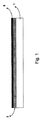
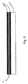
図1に示される本発明の特定の実施形態によれば、二層構造のうちの導電膜(2)が基板(1)と接触している。図2に示される本発明の他の特定の実施形態によれば、UTMF(3)が基板と接触している。 According to the particular embodiment of the invention shown in FIG. 1, the conductive film (2) of the two-layer structure is in contact with the substrate (1). According to another particular embodiment of the invention shown in FIG. 2, the UTMF (3) is in contact with the substrate.
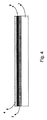
本発明の電極は、他の構造のほかに、図3から図6に示される構造をとることができる。それゆえ、1つの実施形態において、導電膜が本発明の電極の基板の上に堆積される。本発明の他の実施形態によれば、その膜がUTMF膜の上に堆積される。本発明の電極の基板は、その上に二層構造が形成される、あらゆる適当な誘電材料、たとえばガラス、半導体、無機結晶、剛性または柔軟プラスチック材料等とすることができる。たとえば、他のものに加え、シリカ(SiO2)、ボロンシリケート(BK7)、シリコン(Si)、ニオブ酸リチウム(LiNbO3)、ポリエチレンナフタレート(PEN)、ポリエチレンテレフタレート(PET)がある。前記基板は、光電子デバイス構造の一部、たとえば、アクティブ半導体または有機層とすることができる。 The electrode of the present invention can take the structure shown in FIGS. 3 to 6 in addition to other structures. Therefore, in one embodiment, a conductive film is deposited on the substrate of the electrode of the present invention. According to another embodiment of the invention, the film is deposited on a UTMF film. The substrate of the electrode of the present invention can be any suitable dielectric material on which a bilayer structure is formed, such as glass, semiconductor, inorganic crystal, rigid or flexible plastic material, and the like. For example, in addition to others, there are silica (SiO 2 ), boron silicate (BK7), silicon (Si), lithium niobate (LiNbO 3), polyethylene naphthalate (PEN), and polyethylene terephthalate (PET). The substrate can be part of an optoelectronic device structure, such as an active semiconductor or an organic layer.
導電膜は、当業界で周知の方法によって得ることができ、たとえば本発明の電極の隣接する膜または層の上に堆積される。本発明による堆積は、可能な堆積方式の中でも、真空下でのスパッタリングによって有利に実行され、これは、従来のマグネトロンスパッタリング機(Ajaint Orion 3 DC)で行ってもよい。特定の実施形態において、堆積は、DCまたはFRスパッタリング法により、室温の高純度の不活性雰囲気(アルゴン等)内で行われる。
The conductive film can be obtained by methods well known in the art and is deposited, for example, on the adjacent film or layer of the electrode of the present invention. The deposition according to the invention is advantageously carried out by sputtering under vacuum, among possible deposition schemes, which may be performed with a conventional magnetron sputtering machine (
その上に膜が形成される層の、たとえばその上に導電膜が形成される基板の当初の表面粗さは、好ましくは、形成しようとする膜の厚さ以下であるべきであり、そうでない場合、前記導電膜は不連続となり、したがって非導電性となりうる。連続的UTMFをその膜厚と等しいまたはそれより大きい粗さを有する表面上に堆積することは可能であり、その粗さとは、膜厚よりはるかに大きな表面peak−to−valley距離を指す。 The initial surface roughness of the layer on which the film is to be formed, for example the substrate on which the conductive film is to be formed, should preferably be less than or equal to the thickness of the film to be formed In some cases, the conductive film can be discontinuous and therefore non-conductive. It is possible to deposit continuous UTMF on a surface having a roughness equal to or greater than its film thickness, which refers to a surface peak-to-valley distance that is much greater than the film thickness.
本発明の目的にとって、連続性は導電膜にとって必須であり、その一方で極薄金属膜にとっては好ましいが必要ではない。 For the purposes of the present invention, continuity is essential for conductive films, while it is preferred but not necessary for ultrathin metal films.
図3に示される本発明の特定の実施形態によれば、電極は二層構造の導電膜(2)と接触する別の極薄金属膜(3)を有し、この第二のUTMFはニッケル、クロム、金、銀、チタン、カルシウム、プラチナ、マグネシウム、アルミニウム、スズ、インジウム、亜鉛およびこれらの混合物から選択され、第一のUMTFと同じとすることもできる。 According to a particular embodiment of the invention shown in FIG. 3, the electrode has another ultra-thin metal film (3) in contact with the two-layered conductive film (2), this second UTMF being nickel. , Chromium, gold, silver, titanium, calcium, platinum, magnesium, aluminum, tin, indium, zinc and mixtures thereof, and may be the same as the first UMTF.
本発明の特定の実施形態において、電極のUTMFは、随意選択により不動態化される。不動態化処理は、欧州特許出願第0817959号において開示されている安定したUTMFの生成方法によって行われ、この方法には、堆積後のUTMFを周辺空気中、または随意選択により、酸素富化雰囲気中での熱処理が含まれる。保護酸化膜がUTMFの上に形成される。一般に、前記酸化膜は、厚さが通常、0.1から5nmである。適当に酸化されたUTMFにより、下層の導電膜の安定性が増大する。 In certain embodiments of the invention, the electrode UTMF is optionally passivated. The passivation treatment is carried out by the stable UTMF generation method disclosed in European Patent Application No. 0817959, in which the UTMF after deposition is placed in ambient air or, optionally, an oxygen-enriched atmosphere. Includes heat treatment in. A protective oxide film is formed on the UTMF. Generally, the thickness of the oxide film is usually 0.1 to 5 nm. Properly oxidized UTMF increases the stability of the underlying conductive film.
本発明の他の特定の実施形態によれば、電極は導電膜と接触する、または機能金属膜と接触する、別の少なくとも1つの格子または網状構造を含む。前記格子または網状構造は、開口部を有し、欧州特許出願第09382079号に記載されている方法によって得ることができる。この点で、これはその金属の構造の寸法に応じ、各種の方法で製作でき、これにはたとえば、形状制約に応じたUVリソグラフィ、ソフトリソグラフィ(ナノインプリンティング)、スクリーン印刷またはシャドウマスク、あるいはUTMF層またはその他のより厚い層に使用されるものと同様の手法、たとえば蒸着や電気めっきによる堆積がある。このような技術はすべて、当業者によりよく知られている。UTMFは、前述のように、格子または網状構造の堆積の前または後に不動態化することができる。前記格子または網状構造は、Ni、Cr、Ti、Al、Cu、Ag、Au、ZnOドープ、SnO2ドープ、TiO2ドープ、カーボンナノチューブまたはAgナノワイヤまたはこれらの混合物とすることができ、FMFまたは導電膜と同じ材料でも異なる材料でもよい。格子の周期と厚さは、これが周期的金属構造からなる場合、本発明の目的のためには、一般にそれぞれ500nmから1mmおよび10nmから1μmの範囲とすることができる。実際、格子または網状構造の幾何学寸法は、本発明の電極の作製材料と用途のほか、その下の導電膜またはUTMFの厚さおよび関係する局所電流密度に依存する。 According to another particular embodiment of the invention, the electrode comprises another at least one lattice or network that is in contact with the conductive film or in contact with the functional metal film. Said lattice or network has openings and can be obtained by the method described in European Patent Application No. 09382079. In this respect, it can be produced in various ways depending on the dimensions of the metal structure, such as UV lithography, soft lithography (nanoimprinting), screen printing or shadow mask depending on the shape constraints, or There are techniques similar to those used for UTMF layers or other thicker layers, such as vapor deposition or electroplating. All such techniques are well known by those skilled in the art. The UTMF can be passivated before or after the deposition of the lattice or network as described above. The grid or mesh structure may be Ni, Cr, Ti, Al, Cu, Ag, Au, and ZnO doped SnO2 doped, TiO 2 doped carbon nanotubes or Ag nanowire or a mixture thereof, FMF or conductive film The same material or different materials may be used. The period and thickness of the grating can generally be in the range of 500 nm to 1 mm and 10 nm to 1 μm, respectively, for the purposes of the present invention, if this consists of a periodic metal structure. Indeed, the geometric dimensions of the grid or network depend on the material and application of the electrode of the invention as well as the thickness of the underlying conductive film or UTMF and the associated local current density.
好ましくは、金属格子または網状構造の曲線因子は、これが不透明である場合、5%を超えない。随意選択により、格子は正方形、長方形のようなパターン、周期的、またはランダムメッシュの形態をとる。 Preferably, the fill factor of the metal lattice or network does not exceed 5% if it is opaque. Depending on the option, the grid may take the form of a square, rectangular pattern, periodic or random mesh.
図4と図5に示される本発明の別の実施形態において、電極は、UTMF層と接触する少なくとも1つの別の膜(4)を含み、前記膜は、
(i)酸化ニッケル、酸化銅、酸化クロム、酸化チタン、TaまたはNbドープした酸化チタン、酸化カルシウム、酸化マグネシウム、酸化アルミニウム、酸化スズ、Fドープした酸化スズ、酸化インジウム、酸化亜鉛、AlまたはGaドープした酸化亜鉛、ITOおよびこれらの混合物の群から、または、
(ii)Ni、Cr、Au、Ag、Ti、Ca、Pt、Mg、Al、Sn、In、Znおよびこれらの混合物の群から選択される。
In another embodiment of the invention shown in FIGS. 4 and 5, the electrode comprises at least one other membrane (4) in contact with the UTMF layer, said membrane comprising:
(I) Nickel oxide, copper oxide, chromium oxide, titanium oxide, Ta or Nb doped titanium oxide, calcium oxide, magnesium oxide, aluminum oxide, tin oxide, F doped tin oxide, indium oxide, zinc oxide, Al or Ga From the group of doped zinc oxide, ITO and mixtures thereof, or
(Ii) Selected from the group of Ni, Cr, Au, Ag, Ti, Ca, Pt, Mg, Al, Sn, In, Zn and mixtures thereof.
前記膜が上記群(i)から選択された場合、これは随意選択により、UTMFの酸化によって、またはたとえば、対応する酸化物のバルク材料からの直接堆積によって得ることができる。 If the film is selected from group (i) above, this can optionally be obtained by oxidation of UTMF or, for example, by direct deposition from the bulk material of the corresponding oxide.
あるいは、前記膜が金属、すなわちニッケル、クロム、金、銀、チタン、カルシウム、プラチナ、マグネシウム、アルミニウム、スズ、インジウム、亜鉛またはこれらの混合物である場合、酸化膜は、スパッタリング、蒸着およびその他、当業者にとって周知の堆積方法により得ることができる。 Alternatively, if the film is a metal, i.e. nickel, chromium, gold, silver, titanium, calcium, platinum, magnesium, aluminum, tin, indium, zinc, or a mixture thereof, the oxide film may be sputtered, deposited and otherwise. It can be obtained by deposition methods well known to those skilled in the art.
前記別の膜(4)は一般に、厚さが2から200nmの範囲内である。 Said further film (4) is generally in the range of 2 to 200 nm in thickness.
本発明の電極のある特定の実施形態において、電極は、導電層の両側のUTMFと、2つの別の膜(4)からなり、これは同じであっても異なっていてもよく、各々、UTMFと接触する(図6参照)。 In certain embodiments of the electrode of the present invention, the electrode consists of UTMF on either side of the conductive layer and two separate membranes (4), which may be the same or different, each of which is UTMF. (Refer to FIG. 6).
Cu導電膜の透過率と電気シート抵抗は、実践的用途のための範囲内である(>70%、<50Ω/スクエア)。 The transmittance and electrical sheet resistance of the Cu conductive film are within the range for practical use (> 70%, <50Ω / square).
本発明の特定の実施形態によれば、本発明の電極は、厚さ3から20nmの透明なCu導電膜であり、好ましくは厚さ4から10nm、より好ましくは5.5から6.5nmのCuであり、これは、それ以下では膜構造が不連続の島状に見え、それ以上では膜が連続し、導電性を有する、膜の浸透厚さである。 According to certain embodiments of the present invention, the electrode of the present invention is a transparent Cu conductive film having a thickness of 3 to 20 nm, preferably 4 to 10 nm, more preferably 5.5 to 6.5 nm. Cu, which is the penetration thickness of the film below which the film structure looks like discontinuous islands, above which the film is continuous and conductive.
特定の実施形態において、厚さが4から10nmの間のCu膜には、UTMFとして、厚さ3から5nmのTiが形成される。好ましくは、前記Ti膜にはO2処理が施されている。また好ましくは、O2処理済みのTi機能金属膜には、アニーリングが行われている(たとえば、120℃で1時間)。より有利な態様として、Cu膜は6.5〜5.5nmである。前記電極は、シート抵抗が<30Ω/□、ピーク透過率が80%超となりうる。 In a specific embodiment, a Cu film having a thickness of 4 to 10 nm is formed with Ti having a thickness of 3 to 5 nm as UTMF. Preferably, the Ti film is subjected to O 2 treatment. Preferably, the O 2 -treated Ti functional metal film is annealed (for example, at 120 ° C. for 1 hour). As a more advantageous aspect, the Cu film has a thickness of 6.5 to 5.5 nm. The electrode may have a sheet resistance of <30Ω / □ and a peak transmittance of over 80%.
また、厚さ4から10nmのCu膜と厚さ1〜3nmのNi UTMFも好ましい。より有利な態様として、Cu膜は6.5〜6.6nmである。前記Ni UTMFには、アニーリング(たとえば、120℃で1時間)を施しておくことができ、これによってきわめて高い耐熱特性を示し、これはCu膜を安定化させ、シート抵抗を維持し、光透過率を若干改善することができる。このような電極は過酷な環境下におけるデバイス用途において有益である。 Further, a Cu film having a thickness of 4 to 10 nm and a Ni UTMF having a thickness of 1 to 3 nm are also preferable. As a more advantageous aspect, the Cu film has a thickness of 6.5 to 6.6 nm. The Ni UTMF can be annealed (eg, 1 hour at 120 ° C.), thereby exhibiting extremely high heat resistance, which stabilizes the Cu film, maintains sheet resistance, and transmits light. The rate can be slightly improved. Such electrodes are useful in device applications in harsh environments.
他の好ましい実施形態によれば、電極はCu導電膜、FMFおよび、5から200nmの範囲内の少なくとも1つの酸化膜を有する透明電極である。 According to another preferred embodiment, the electrode is a Cu conductive film, FMF and a transparent electrode having at least one oxide film in the range of 5 to 200 nm.
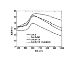
以下の説明において、特に断りがないかぎり、可視光透過率(VOT)は、375から700nmの範囲の平均値であり、基板寄与分が差し引かれている。図中、第一と第二の数はそれぞれ、CuとUTMFの厚さである。 In the following description, unless otherwise specified, the visible light transmittance (VOT) is an average value in the range of 375 to 700 nm, and the substrate contribution is subtracted. In the figure, the first and second numbers are the thicknesses of Cu and UTMF, respectively.
発明者らは、以下を開示している。
UTMFがCu膜と一緒に使用されて、本発明の二層構造を形成する場合、Cu膜の電気的および光学的性能は基本的に維持される(図7と図8)。図7においては、可視光透過率(VOT)が電気的シート抵抗(Ω/□)に対して表されている。実際に、たとえば、Ni−UTMFを使用することによって、作業関数が増大し、透明電極(TE)はOLED用のアノードとして、より適したものとなる。図8において、透過率が波長(nm)に対して表されている。発明者らはまた、高温にさらされた場合、Cu+Ni(7+1)のような二層構造のCu+FMFではなく、Cu膜の光学的および電気的性能を劣化させることを開示しており、これは図9と図10および下表1において示されている。
The inventors disclose the following.
When UTMF is used with a Cu film to form the bilayer structure of the present invention, the electrical and optical performance of the Cu film is essentially maintained (FIGS. 7 and 8). In FIG. 7, the visible light transmittance (VOT) is expressed with respect to the electrical sheet resistance (Ω / □). In fact, for example, using Ni-UTMF increases the work function and makes the transparent electrode (TE) more suitable as an anode for OLEDs. In FIG. 8, the transmittance is expressed with respect to the wavelength (nm). The inventors have also disclosed that when exposed to high temperatures, the optical and electrical performance of the Cu film, rather than a two-layered Cu + FMF such as Cu + Ni (7 + 1), is degraded. 9 and FIG. 10 and Table 1 below.

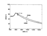
図7において、SWNTに沿った二層構造(Cu−Ni/Ti)とグラフェン膜からなる本発明による電極の性能が比較されている。1nmのNi−FMFによって透過率が約10%低下しているのに対し、Ti−FMFを用いると、シート抵抗がさほど変化せずに透過率が増大することがわかる。この挙動は、NiおよびTi極薄膜の屈折率マッチングと吸光係数の違いの点で説明することができる。極薄Ti膜は、Ni膜と比較して、屈折率が低く、吸光係数がはるかに小さいため、吸収率が低く、界面反射が低い。実際の極薄金属膜において、抵抗の理論的モデルはあまり役に立たず、これは、表面散乱を促進する形状限界(サイズ効果)のほかに、抵抗はまた、粒界、空乏および不連続性等の散乱の容積線源に依存し、それ自体が堆積条件による影響を受けやすいからである。したがって、膜のシート抵抗が最も低くなるような堆積条件を最適化してもよい。これら4つのサンプル群の導電挙動は主として、下層のCu極薄導電膜が連続的(>5nm)になると、この膜によって起こされることがわかる。 In FIG. 7, the performance of the electrode according to the present invention consisting of a bilayer structure (Cu—Ni / Ti) along with SWNT and a graphene film is compared. It can be seen that the transmittance is reduced by about 10% with 1 nm Ni-FMF, whereas the transmittance is increased without changing the sheet resistance when Ti-FMF is used. This behavior can be explained in terms of the difference in refractive index matching and extinction coefficient of Ni and Ti ultrathin films. An ultra-thin Ti film has a lower refractive index and a much smaller extinction coefficient than an Ni film, and therefore has a low absorption rate and low interface reflection. In actual ultra-thin metal films, the theoretical model of resistance is not very useful, in addition to the shape limit (size effect) that promotes surface scattering, the resistance is also not limited to grain boundaries, depletion and discontinuities. This is because it depends on the volume source of scattering and is itself susceptible to deposition conditions. Therefore, the deposition conditions that minimize the sheet resistance of the film may be optimized. It can be seen that the conductive behavior of these four sample groups is mainly caused by this film when the underlying Cu ultrathin conductive film becomes continuous (> 5 nm).
Cu+Ti3に対するO2処理は、Tiのうちの上から数ナノメートルだけを酸化し、CuとTiの界面を妨害しない。Ti酸化物の形成は、下層のCu層を酸化から保護するだけでなく、透過率も増大させる。Cu6+Ti3(O2処理済み)サンプルのピーク透過率とシート抵抗はそれぞれ、630nmで>86%と300Ω/□である。この結果は、Ni極薄金属層について報告されているものよりはるかによい。しかしながら、Niの高い仕事関数が重要な役割を果たすような、底部電極としてITOまたはNi極薄金属膜のいずれかを備えるデバイスについても、同様の効率が得られた。UTMFを適正に選択し、必要に応じてこれを酸化することにより、デバイスの構成に合わせて透明導電体の仕事関数を調整できる。これに加えて、図7から、極薄Cuをベースとする透明導電体は、現在、TCOの代用としての可能性が高いと考えられているSWNTとグラフェン膜よりよいことが明らかである。異なる透明導電体群の性能を比較するために、Haackeにより定義される性能指数ΦTCの数値を計算した。
図11は、異なるサンプル群の性能指数を示す。Cu+Ti2(O2処理済み)のサンプルは、ΦTCのピーク値が2.5×10⁻³Ω−1である。すべてのデータセットにおいて、最良の性能指数は、厚さ5.5から6.5nmのCuについて得られ、これはCuがこの範囲において連続的となることを示している。これをさらに確認するために、異なるサンプル群についてのRSt3対t(tは膜厚)15をグラフにすることにより、浸透閾値を概算した(図11の差し込み図)。すべてのセットの浸透閾値が5.5nmから6.5nmの間であることがわかり、これは発明者による上記の予測をさらに裏付けるものである。各セットについて、Cuの厚さを浸透厚さから特定された6.5nmに固定し(図11の差し込み図)、1つのサンプルを堆積させた。AFMによって測定した4つすべてのサンプルのRMS粗さのpeak−to−valley値は、膜厚よりはるかに小さかった。 FIG. 11 shows the figure of merit for different sample groups. Sample Cu + Ti2 (O 2 treated), the peak value of [Phi TC is 2.5 × 10 -3 Ω -1. In all data sets, the best figure of merit is obtained for Cu with a thickness of 5.5 to 6.5 nm, indicating that Cu is continuous in this range. To further confirm this, the penetration threshold was approximated by graphing R S t 3 vs. t (t is the film thickness) 15 for different sample groups (inset of FIG. 11). It can be seen that the penetration threshold for all sets is between 5.5 nm and 6.5 nm, which further supports the above prediction by the inventors. For each set, the Cu thickness was fixed at 6.5 nm determined from the penetration thickness (inset of FIG. 11), and one sample was deposited. The RMS roughness peak-to-valley values of all four samples measured by AFM were much smaller than the film thickness.
図12は、これらすべてのサンプル透過率スペクトルを示す。可視光領域における異なる光透過率挙動は、反射率と吸収率の点で説明することができる。 FIG. 12 shows all these sample transmission spectra. Different light transmittance behaviors in the visible light region can be explained in terms of reflectance and absorptance.
図13は、可視光領域におけるこれら4つのすべてのサンプルの平均反射率と吸収率を比較する。吸収率は、A=1−(T+R)を用いて計算した。Ni−FMFを除くすべてのサンプルが同様の吸収率を見せたが、興味深い点として、in−situO2プラズマ処理が施されたサンプルは反射率が低く、これはその高い透過率を説明するものである。Ni−FMFは反射率が高いほか、吸収率も高く、その結果、他の3つのサンプルより透過率が低い。サンプルの安定性を評価するために、これらを炉内で120℃の周辺雰囲気中に60分保持した。熱処理後に透過率の上昇とこれに伴うシート抵抗の増大を見せた他の3つのサンプルと異なり、Cu6.5+Ni1のシート抵抗と可視光透過率はほとんど影響を受けず、実際には若干改善されたことがわかった。わずか1nmのNi FMFでも、下層のCuを過酷な環境下における酸化から十分に保護することが明らかである。図13の差し込み図は、Cu6.5+Ni1の熱処理前(実線)と熱処理後(破線)の可視光領域のスペクトルを示している。電気的および光学的特性の両方における小さな改善は、界面結晶化度の改善によるものであろう。 FIG. 13 compares the average reflectance and absorptance of all four samples in the visible light region. Absorptivity was calculated using A = 1- (T + R). All samples except Ni-FMF showed similar absorptance, but interestingly, the in-situ O 2 plasma treated sample has low reflectivity, which explains its high transmittance. is there. Ni-FMF has high reflectivity and high absorptance, and as a result, the transmittance is lower than the other three samples. In order to evaluate the stability of the samples, they were kept in a furnace at 120 ° C. in an ambient atmosphere for 60 minutes. Unlike the other three samples, which showed an increase in transmittance and a corresponding increase in sheet resistance after heat treatment, the sheet resistance and visible light transmittance of Cu6.5 + Ni1 were hardly affected and actually improved slightly. I understood it. It is clear that even 1 nm Ni FMF can sufficiently protect the underlying Cu from oxidation in harsh environments. The inset of FIG. 13 shows the spectrum of the visible light region before heat treatment (solid line) and after heat treatment (broken line) of Cu6.5 + Ni1. Small improvements in both electrical and optical properties may be due to improved interface crystallinity.
図14において、O2処理されたCu 6.5nm+Ti 5nmの、堆積時と120℃で60分のアニーリング後の透過率を比較する。このグラフから、アニーリング処理を行っても可視光領域における膜の透過率は大きく変化しないことが明らかである。膜のシート抵抗は、アニーリングによって若干のみ増大した(15.9から19.8Ω/□となった)。それゆえ、5nmの酸化Ti FMFは下層のCuを過酷な環境下での酸化から現実的に保護することが明らかである。
In FIG. 14, the transmittance of Cu 6.5 nm +
結論として、導電性金属膜とUTMFからなる安価で、製造しやすく、安定した電極は、各種の光電子分野の用途にとって好適な透明導電体である。本発明の電極は、可視光領域における平均透過率が75%と高く、また、シート抵抗は20Ω/□と低い。Cuをベースとする二層電極の性能指数ΦTCは、SWNTおよびグラフェン膜よりよいことがわかった。Cu+Ni1およびO2処理されたCu+Ti5のサンプルは、炉内で120℃の周囲雰囲気中、60分の熱処理を行った後であっても、優れた安定性見せた。 In conclusion, an inexpensive, easy-to-manufacture, stable electrode made of a conductive metal film and UTMF is a suitable transparent conductor for various optoelectronic applications. The electrode of the present invention has a high average transmittance in the visible light region of 75% and a low sheet resistance of 20Ω / □. It has been found that the figure of merit Φ TC of the two-layer electrode based on Cu is better than that of SWNT and graphene film. Cu + Ni1 and O 2 treated Cu + Ti5 samples showed excellent stability even after 60 minutes heat treatment in an ambient atmosphere at 120 ° C. in a furnace.
発明者らは、先行技術の既存の電極の欠点を持たない材料、特にCuまたはその他同様の導電材料の電気的および光学的特性を探ることができた。この意味において、本発明の電極は安定した透明な導電性電極であり、その単純で低コストの構造および製造方法ならびにその本来的な技術的特性から、その多くの用途が見出される。電極の安定性は、特に要求の厳しい、変化する環境条件下で、デバイスの性能を長期間維持する上で最も重要である。本発明の透明電極はそれゆえ、さまざまなデバイスに使用可能である。 The inventors have been able to explore the electrical and optical properties of materials that do not have the drawbacks of existing electrodes of the prior art, in particular Cu or other similar conductive materials. In this sense, the electrode of the present invention is a stable transparent conductive electrode, and its many uses are found due to its simple and low cost structure and manufacturing method and its inherent technical properties. Electrode stability is most important in maintaining device performance for extended periods, especially under demanding and changing environmental conditions. The transparent electrode of the present invention can therefore be used in various devices.
他の態様において、本発明は、少なくとも前述の電極を備える光電子デバイスに関する。前記デバイスとしては、発光ダイオード(LED)、有機発光ダイオード(OLED)、ディスプレイ、光電池、光検出器、光変調器、エレクトロクロミックデバイス、電子ペーパ、タッチスクリーン、電磁波シールド層、透明またはスマート(たとえば、省エネルギー、デフォーカシング)ウィンドウ等がある。 In another aspect, the invention relates to an optoelectronic device comprising at least the aforementioned electrode. The devices include light emitting diodes (LEDs), organic light emitting diodes (OLEDs), displays, photovoltaic cells, photodetectors, light modulators, electrochromic devices, electronic paper, touch screens, electromagnetic shielding layers, transparent or smart (e.g., Energy saving, defocusing) window.
上記は、本発明を例示するものである。しかしながら、本発明は、本明細書に記載の以下の詳細な実施形態に限定されず、末尾の特許請求の範囲に含まれるすべての同等の変更を包含する。 The above is illustrative of the invention. However, the present invention is not limited to the following detailed embodiments described herein, but includes all equivalent variations that fall within the scope of the appended claims.
図1に描かれた実施形態に対応する本発明による電極を製作した。光学的に両面研磨されたUV溶融石英基板をまず、それぞれアセトンとエタノールを用いた超音波バスの中で10分間洗浄し、その後、窒素ガンで乾燥させた。清浄な基板を次に、スパッタリングシステム(Ajait Orion 3 DC)のメインチャンバに装填し、圧力レベルを1.33×10⁻⁶Pa(10−8トール)のオーダまで下げた。スパッタリングは、室温、0.226Pa(2mトール)の高純度アルゴン雰囲気中、100WのDC電源で行った。ターゲットの純度レベルは99.99%である。堆積前に、基板を再び、バックグラウンド圧(base pressure)1.06Pa(8mトール)、40WのRF電源の酸素プラズマで15分間洗浄した。
An electrode according to the present invention was fabricated corresponding to the embodiment depicted in FIG. The optically double-side polished UV fused quartz substrate was first washed for 10 minutes in an ultrasonic bath using acetone and ethanol, respectively, and then dried with a nitrogen gun. The clean substrate was then loaded into the main chamber of the sputtering system (
DCスパッタリングによってCuとNiを堆積させ、その一方で、FRスパッタリングによりTiを形成した。厚さを、MCM−160水晶でモニタした。堆積速度は、Cuについては1.5Å/s、Niについては0.573Å/s、Tiについては0.083Å/sとした。これらの電極において、導電膜は厚さ3〜10nmのCu、機能金属膜は厚さ1nmから5nmのNiまたはTiであった。 Cu and Ni were deposited by DC sputtering, while Ti was formed by FR sputtering. Thickness was monitored with MCM-160 quartz. The deposition rate was 1.5 Å / s for Cu, 0.573 Å / s for Ni, and 0.083 Å / s for Ti. In these electrodes, the conductive film was Cu having a thickness of 3 to 10 nm, and the functional metal film was Ni or Ti having a thickness of 1 to 5 nm.
特に、4種類の厚さのCuを製作した。すなわち、Cu、Cuとその上の1nmのNi、Cuとその上の1nmのTi、Cuとその上の3nmのTi、Cuとその上の5nmのTiであり、以下、それぞれをCu、Cu+Ni1、Cu+Ti1、Cu+Ti3、Cu+Ti5と表す。Cuの上に3および5nmのTiを堆積したものに、動作圧力8mT、40WのRF電源のO2プラズマで15分間、in situ酸化を行った(以下、「O2処理済み」と呼ぶ)。Perkin Elmer Iambda 950分光計を使用して、透過率スペクトルを測定し、その一方で、Cascade Microtech 44/7 S 2749の4点プローブシステムおよびKeithley 2001マルチメータでシート抵抗を測定した。製作された膜は、原子間力顕微鏡(AFM)により、デジタル計測器D3100 AFMおよびこれに関連するソフトウェア、WsXMで特徴付けた。 In particular, four types of thickness Cu were produced. That is, Cu, Cu and 1 nm Ni thereon, Cu and 1 nm Ti above, Cu and 3 nm Ti above, Cu and 5 nm Ti above, respectively, Cu, Cu + Ni1, It represents as Cu + Ti1, Cu + Ti3, Cu + Ti5. In-situ oxidation was performed for 15 minutes using an O 2 plasma of an RF power source with an operating pressure of 8 mT and 40 W on Ti and 3 nm Ti deposited on Cu (hereinafter referred to as “O 2 treated”). Transmission spectra were measured using a Perkin Elmer Imbda 950 spectrometer, while sheet resistance was measured with a Cascade Microtech 44/7 S 2749 4-point probe system and a Keithley 2001 multimeter. The fabricated membrane was characterized by digital instrument D3100 AFM and associated software, WsXM, by atomic force microscopy (AFM).
Claims (13)
前記導電膜がCu、Au、Ag、Alおよびこれらの混合物から選択され、
前記超薄型金属薄膜がNi、Cr、Ti、Pt、Ag、Au、Alおよびこれらの混合物から選択されることを特徴とする電極。 In an electrode comprising a substrate (1) and a layered structure made of a conductive film (2) in contact with at least one ultrathin metal film (3), the two films being different materials,
The conductive film is selected from Cu, Au, Ag, Al and mixtures thereof;
The electrode characterized in that the ultra-thin metal thin film is selected from Ni, Cr, Ti, Pt, Ag, Au, Al and mixtures thereof.
前記導電膜および/または前記極薄金属膜が光学的に透明であることを特徴とする電極。 The electrode according to claim 1, wherein
The electrode, wherein the conductive film and / or the ultrathin metal film is optically transparent.
極薄金属膜が、周囲雰囲気中、またはO2富化雰囲気中で熱処理されていることを特徴とする電極。 In the electrode according to any one of the preceding items,
An ultra-thin metal film is heat-treated in an ambient atmosphere or an O 2 enriched atmosphere.
前記層状構造の上に金属格子または網状構造をさらに備えることを特徴とする電極。 In the electrode according to any one of the preceding items,
The electrode further comprising a metal lattice or a net-like structure on the layered structure.
前記導電膜がCuであることを特徴とする電極。 In the electrode according to any one of the preceding items,
The electrode, wherein the conductive film is Cu.
前記極薄金属膜がNiであることを特徴とする電極。 The electrode according to claim 5, wherein
An electrode characterized in that the ultrathin metal film is Ni.
前記極薄金属膜がTiであることを特徴とする電極。 The electrode according to claim 5, wherein
An electrode characterized in that the ultrathin metal film is Ti.
前記Cu膜が4から10nmの厚さであり、前記Ni極薄金属膜が1から3nmの厚さであることを特徴とする電極。 The electrode according to claim 6.
The electrode, wherein the Cu film has a thickness of 4 to 10 nm, and the Ni ultrathin metal film has a thickness of 1 to 3 nm.
前記Cu膜が4から10nmの厚さであり、前記Ti極薄金属膜が3から5nmの厚さであることを特徴とする電極。 The electrode according to claim 7.
The electrode characterized in that the Cu film is 4 to 10 nm thick and the Ti ultra-thin metal film is 3 to 5 nm thick.
極薄金属膜を1つのみ有し、前記導電膜のほうが前記基板に近いことを特徴とする電極。 In the electrode according to any one of the preceding items,
An electrode having only one ultrathin metal film, wherein the conductive film is closer to the substrate.
極薄金属膜を1つのみ有し、前記極薄金属膜のほうが前記基板に近いことを特徴とする電極。 The electrode according to any one of claims 1 to 9,
An electrode having only one ultrathin metal film, wherein the ultrathin metal film is closer to the substrate.
少なくとも1つの極薄金属層と接触する少なくとも1つの別の膜(4)をさらに備え、前記別の膜が、
(i)酸化ニッケル、酸化銅、酸化クロム、酸化チタン、TaまたはNbドープした酸化チタン、酸化カルシウム、酸化マグネシウム、酸化アルミニウム、酸化スズ、Fドープした酸化スズ、酸化インジウム、酸化亜鉛、AlまたはGaドープした酸化亜鉛、ITOおよびこれらの混合物の群から、または、
(ii)Ni、Cr、Au、Ag、Ti、Ca、Pt、Mg、Al、Sn、In、Znおよびこれらの混合物の群から選択されることを特徴とする電極。 In the electrode according to any one of the preceding items,
At least one further membrane (4) in contact with at least one ultrathin metal layer, said further membrane comprising:
(I) Nickel oxide, copper oxide, chromium oxide, titanium oxide, Ta or Nb doped titanium oxide, calcium oxide, magnesium oxide, aluminum oxide, tin oxide, F doped tin oxide, indium oxide, zinc oxide, Al or Ga From the group of doped zinc oxide, ITO and mixtures thereof, or
(Ii) An electrode selected from the group consisting of Ni, Cr, Au, Ag, Ti, Ca, Pt, Mg, Al, Sn, In, Zn, and mixtures thereof.
Applications Claiming Priority (3)
| Application Number | Priority Date | Filing Date | Title |
|---|---|---|---|
| EP09382238A EP2317562A1 (en) | 2009-11-03 | 2009-11-03 | Multilayer metallic electrodes for optoelectronics |
| EP09382238.5 | 2009-11-03 | ||
| PCT/EP2010/066625 WO2011054814A1 (en) | 2009-11-03 | 2010-11-02 | Multilayer metallic electrodes for optoelectronics |
Publications (2)
| Publication Number | Publication Date |
|---|---|
| JP2013510397A true JP2013510397A (en) | 2013-03-21 |
| JP2013510397A5 JP2013510397A5 (en) | 2013-12-19 |
Family
ID=42226549
Family Applications (1)
| Application Number | Title | Priority Date | Filing Date |
|---|---|---|---|
| JP2012537367A Withdrawn JP2013510397A (en) | 2009-11-03 | 2010-11-02 | Multilayer metal electrodes for optoelectronic devices |
Country Status (5)
| Country | Link |
|---|---|
| US (1) | US20120260983A1 (en) |
| EP (1) | EP2317562A1 (en) |
| JP (1) | JP2013510397A (en) |
| KR (1) | KR20120098739A (en) |
| WO (1) | WO2011054814A1 (en) |
Cited By (3)
| Publication number | Priority date | Publication date | Assignee | Title |
|---|---|---|---|---|
| JP2014038920A (en) * | 2012-08-14 | 2014-02-27 | Toshiba Corp | Semiconductor light-emitting element |
| JP2017079462A (en) * | 2015-08-03 | 2017-04-27 | フンダシオ インスティチュート デ サイエンセズ フォトニクス | Image sensor with non-local readout circuit and optoelectronic device comprising this image sensor |
| JP2018060787A (en) * | 2016-09-30 | 2018-04-12 | エルジー ディスプレイ カンパニー リミテッド | Electrode, organic light-emitting device including the same, liquid crystal display device, and organic light-emitting display device |
Families Citing this family (20)
| Publication number | Priority date | Publication date | Assignee | Title |
|---|---|---|---|---|
| JP2013064713A (en) * | 2011-08-30 | 2013-04-11 | Canon Inc | X-ray waveguide and x-ray wave-guiding system |
| EP2581789B1 (en) | 2011-10-14 | 2020-04-29 | Fundació Institut de Ciències Fotòniques | Optically transparent and electrically conductive coatings and method for their deposition on a substrate |
| US9296183B2 (en) | 2011-11-30 | 2016-03-29 | Corning Incorporated | Metal dewetting methods and articles produced thereby |
| CN103515397A (en) * | 2012-06-18 | 2014-01-15 | 联咏科技股份有限公司 | An image sensing device with pixel level automatic optical attenuators |
| KR20140034545A (en) * | 2012-09-12 | 2014-03-20 | 삼성전기주식회사 | Touch panel |
| WO2014140297A1 (en) * | 2013-03-14 | 2014-09-18 | Fundació Institut De Ciències Fotòniques | Transparent electrode and substrate for optoelectronic or plasmonic applications comprising silver |
| CN103578782A (en) * | 2013-11-08 | 2014-02-12 | 蚌埠玻璃工业设计研究院 | Method for improving light absorption efficiency of nano crystal TiO2 electrode of dye-sensitized cell |
| US20160002096A1 (en) | 2014-07-02 | 2016-01-07 | Corning Incorporated | Silicon and silica nanostructures and method of making silicon and silica nanostructures |
| US20160139699A1 (en) * | 2014-11-16 | 2016-05-19 | Microsoft Technology Licensing, Llc | Light sensitive digitizer system |
| CN105810842B (en) * | 2014-12-29 | 2019-01-11 | 昆山国显光电有限公司 | The anode construction of Organic Light Emitting Diode |
| US10097281B1 (en) | 2015-11-18 | 2018-10-09 | Hypres, Inc. | System and method for cryogenic optoelectronic data link |
| CN107768483B (en) * | 2017-10-30 | 2019-10-11 | 河南科技大学 | A kind of preparation method of full printing zinc oxide ultraviolet detector |
| JP7052487B2 (en) * | 2018-03-29 | 2022-04-12 | 住友大阪セメント株式会社 | Optical element |
| CN112582483A (en) * | 2019-09-30 | 2021-03-30 | 康宁股份有限公司 | Transparent conductor materials with enhanced near infrared properties and methods of forming the same |
| CN111682114A (en) * | 2020-06-16 | 2020-09-18 | 电子科技大学 | Organic photoelectric detector bottom electrode and preparation method and application thereof |
| CN112086532B (en) * | 2020-10-15 | 2021-10-22 | 湖北大学 | SnO2Basic homojunction self-driven ultraviolet photoelectric detector and preparation method thereof |
| CN112259278B (en) * | 2020-10-19 | 2022-05-03 | 西安工程大学 | Preparation method of particle composite fiber reinforced copper tin oxide contact material |
| CN112768617A (en) * | 2021-01-06 | 2021-05-07 | 武汉华星光电半导体显示技术有限公司 | Display panel, preparation method thereof and display device |
| CN114242981B (en) * | 2021-12-17 | 2024-04-09 | 太原理工大学 | TiO (titanium dioxide) 2 -SnO 2 Composite material, preparation method and application thereof |
| CN114823930B (en) * | 2022-03-24 | 2023-04-11 | 电子科技大学 | Amorphous Ga based on MgO passivation 2 O 3 Solar blind ultraviolet detector and preparation method thereof |
Family Cites Families (13)
| Publication number | Priority date | Publication date | Assignee | Title |
|---|---|---|---|---|
| US4345107A (en) * | 1979-06-18 | 1982-08-17 | Ametek, Inc. | Cadmium telluride photovoltaic cells |
| US5486857A (en) * | 1989-08-15 | 1996-01-23 | Minnesota Mining And Manufacturing Company | Thermal imaging system |
| DE4427215A1 (en) * | 1993-08-02 | 1995-02-23 | Agency Ind Science Techn | Transparent and conductive ultrathin films and process for the production thereof |
| DE19520843A1 (en) * | 1995-06-08 | 1996-12-12 | Leybold Ag | Disc made of translucent material and process for its manufacture |
| US6208400B1 (en) * | 1996-03-15 | 2001-03-27 | Canon Kabushiki Kaisha | Electrode plate having metal electrodes of aluminum or nickel and copper or silver disposed thereon |
| DE19958878B4 (en) * | 1999-12-07 | 2012-01-19 | Saint-Gobain Glass Deutschland Gmbh | Thin film solar cell |
| KR20040021590A (en) * | 2001-03-16 | 2004-03-10 | 니혼 이타가라스 가부시키가이샤 | Metallic very thin film, metallic very thin film multilayer body, and method for manufacturing the metallic very thin film or the metallic very thin film laminate |
| US6919133B2 (en) * | 2002-03-01 | 2005-07-19 | Cardinal Cg Company | Thin film coating having transparent base layer |
| DE10308515B4 (en) * | 2003-02-26 | 2007-01-25 | Schott Ag | Method for producing organic light-emitting diodes and organic light-emitting diode |
| DE602004032509D1 (en) * | 2004-01-13 | 2011-06-16 | Sanyo Electric Co | Photovoltaic device |
| CN101438199A (en) * | 2004-10-25 | 2009-05-20 | 加利福尼亚大学董事会 | Stacked layer electrode for organic electronic devices |
| ITRM20060181A1 (en) * | 2006-03-31 | 2007-10-01 | Pilkington Italia Spa | GLAZED GLASS SHEET |
| KR20090091175A (en) * | 2006-11-17 | 2009-08-26 | 쌩-고벵 글래스 프랑스 | Electrode for an organic light-emitting device, acid etching thereof, and also organic light-emitting device incorporating it |
-
2009
- 2009-11-03 EP EP09382238A patent/EP2317562A1/en not_active Withdrawn
-
2010
- 2010-11-02 KR KR1020127013249A patent/KR20120098739A/en not_active Application Discontinuation
- 2010-11-02 WO PCT/EP2010/066625 patent/WO2011054814A1/en active Application Filing
- 2010-11-02 US US13/505,374 patent/US20120260983A1/en not_active Abandoned
- 2010-11-02 JP JP2012537367A patent/JP2013510397A/en not_active Withdrawn
Cited By (4)
| Publication number | Priority date | Publication date | Assignee | Title |
|---|---|---|---|---|
| JP2014038920A (en) * | 2012-08-14 | 2014-02-27 | Toshiba Corp | Semiconductor light-emitting element |
| JP2017079462A (en) * | 2015-08-03 | 2017-04-27 | フンダシオ インスティチュート デ サイエンセズ フォトニクス | Image sensor with non-local readout circuit and optoelectronic device comprising this image sensor |
| JP2018060787A (en) * | 2016-09-30 | 2018-04-12 | エルジー ディスプレイ カンパニー リミテッド | Electrode, organic light-emitting device including the same, liquid crystal display device, and organic light-emitting display device |
| US10847742B2 (en) | 2016-09-30 | 2020-11-24 | Lg Display Co., Ltd. | Electrode, organic light emitting diode, liquid crystal display device, and organic light emitting display device of the same |
Also Published As
| Publication number | Publication date |
|---|---|
| EP2317562A1 (en) | 2011-05-04 |
| EP2317562A8 (en) | 2011-08-10 |
| KR20120098739A (en) | 2012-09-05 |
| WO2011054814A1 (en) | 2011-05-12 |
| US20120260983A1 (en) | 2012-10-18 |
Similar Documents
| Publication | Publication Date | Title |
|---|---|---|
| JP2013510397A (en) | Multilayer metal electrodes for optoelectronic devices | |
| KR101680928B1 (en) | Transparent electrode based on combination of transparent conductive oxides, metals and oxides | |
| JP4888119B2 (en) | Transparent conductive film and method for producing the same, transparent conductive substrate, and light-emitting device | |
| KR101621571B1 (en) | Method to prepare a stable transparent electrode | |
| Ghosh et al. | High figure-of-merit Ag/Al: ZnO nano-thick transparent electrodes for indium-free flexible photovoltaics | |
| US20120103669A1 (en) | Metal transparent conductors with low sheet resistance | |
| JP4971618B2 (en) | Display electrode pattern manufacturing method | |
| Dimopoulos et al. | Properties of transparent and conductive Al: ZnO/Au/Al: ZnO multilayers on flexible PET substrates | |
| Lansåker et al. | Thin sputter deposited gold films on In2O3: Sn, SnO2: In, TiO2 and glass: Optical, electrical and structural effects | |
| Li et al. | High-performance flexible transparent conductive thin films on PET substrates with a CuM/AZO structure | |
| KR101519888B1 (en) | Hybrid transparent electrode and the fabricating method thereof | |
| KR20150039373A (en) | Transparent electode and electronic device comprising the same | |
| Yu et al. | Enhanced conductivity and stability of Cu-embedded zinc tin oxide flexible transparent conductive thin films | |
| Wang et al. | Fabrication and thermo stability of the SnO2/Ag/SnO2 tri-layer transparent conductor deposited by magnetic sputtering | |
| JP2007163995A (en) | Substrate with transparent conductive film and manufacturing method thereof | |
| Cho et al. | Nanoscale silver-based Al-doped ZnO multilayer transparent-conductive oxide films | |
| JP3725908B2 (en) | Conductive laminate | |
| CN111883284A (en) | Double-sided conductive film, film coating method and touch screen | |
| EP2973728B1 (en) | Transparent electrode and substrate for optoelectronic or plasmonic applications comprising silver | |
| JP3850865B2 (en) | Conductive laminate | |
| KR101051662B1 (en) | Transparent conductive film with excellent bending characteristics, transparent electrode and organic electronic device using same | |
| CN108766631A (en) | A kind of laminated film | |
| Lee et al. | Highly transparent and flexible TiN doped In2O3 (ITON)/Ag-Ti/ITON multilayer electrodes coated on polyethylene terephthalate substrate | |
| KR101104675B1 (en) | A Hole transporting layer for Light emitting devices and method for manufacturing thereof | |
| Qin et al. | Effect of structural design on the electrical, optical and mechanical properties of flexible BaSnO3–Ag composite thin films |
Legal Events
| Date | Code | Title | Description |
|---|---|---|---|
| A521 | Request for written amendment filed |
Free format text: JAPANESE INTERMEDIATE CODE: A523 Effective date: 20131029 |
|
| A621 | Written request for application examination |
Free format text: JAPANESE INTERMEDIATE CODE: A621 Effective date: 20131029 |
|
| A761 | Written withdrawal of application |
Free format text: JAPANESE INTERMEDIATE CODE: A761 Effective date: 20131119 |