JP2013228303A - Sample analysis element and detector - Google Patents
Sample analysis element and detector Download PDFInfo
- Publication number
- JP2013228303A JP2013228303A JP2012101021A JP2012101021A JP2013228303A JP 2013228303 A JP2013228303 A JP 2013228303A JP 2012101021 A JP2012101021 A JP 2012101021A JP 2012101021 A JP2012101021 A JP 2012101021A JP 2013228303 A JP2013228303 A JP 2013228303A
- Authority
- JP
- Japan
- Prior art keywords
- nanostructure
- sample analysis
- analysis element
- light
- pitch
- Prior art date
- Legal status (The legal status is an assumption and is not a legal conclusion. Google has not performed a legal analysis and makes no representation as to the accuracy of the status listed.)
- Withdrawn
Links
Images


Classifications
-
- G—PHYSICS
- G01—MEASURING; TESTING
- G01N—INVESTIGATING OR ANALYSING MATERIALS BY DETERMINING THEIR CHEMICAL OR PHYSICAL PROPERTIES
- G01N21/00—Investigating or analysing materials by the use of optical means, i.e. using sub-millimetre waves, infrared, visible or ultraviolet light
- G01N21/01—Arrangements or apparatus for facilitating the optical investigation
- G01N21/03—Cuvette constructions
-
- G—PHYSICS
- G01—MEASURING; TESTING
- G01N—INVESTIGATING OR ANALYSING MATERIALS BY DETERMINING THEIR CHEMICAL OR PHYSICAL PROPERTIES
- G01N21/00—Investigating or analysing materials by the use of optical means, i.e. using sub-millimetre waves, infrared, visible or ultraviolet light
- G01N21/62—Systems in which the material investigated is excited whereby it emits light or causes a change in wavelength of the incident light
- G01N21/63—Systems in which the material investigated is excited whereby it emits light or causes a change in wavelength of the incident light optically excited
- G01N21/65—Raman scattering
- G01N21/658—Raman scattering enhancement Raman, e.g. surface plasmons
-
- G—PHYSICS
- G01—MEASURING; TESTING
- G01N—INVESTIGATING OR ANALYSING MATERIALS BY DETERMINING THEIR CHEMICAL OR PHYSICAL PROPERTIES
- G01N21/00—Investigating or analysing materials by the use of optical means, i.e. using sub-millimetre waves, infrared, visible or ultraviolet light
- G01N21/17—Systems in which incident light is modified in accordance with the properties of the material investigated
- G01N21/55—Specular reflectivity
- G01N21/552—Attenuated total reflection
- G01N21/553—Attenuated total reflection and using surface plasmons
- G01N21/554—Attenuated total reflection and using surface plasmons detecting the surface plasmon resonance of nanostructured metals, e.g. localised surface plasmon resonance
Abstract
Description
本発明は、金属膜で覆われるナノ体を備える試料分析素子、および、そういった試料分析素子を利用した検出装置等に関する。 The present invention relates to a sample analysis element including a nanobody covered with a metal film, a detection apparatus using such a sample analysis element, and the like.
局在表面プラズモン共鳴(LSPR)を利用した試料分析素子は知られる。こうした試料分析素子は例えば金属膜で覆われるナノ体を備える。ナノ体は例えば励起光の波長よりも十分に小さく形成される。ナノ体上の金属膜に励起光が照射されると、全電気双極子が揃い増強電場が誘発される。その結果、金属膜の表面で近接場光が生成される。いわゆるホットスポットが形成される。 Sample analysis elements using localized surface plasmon resonance (LSPR) are known. Such a sample analysis element comprises, for example, a nanobody covered with a metal film. The nanobody is formed, for example, sufficiently smaller than the wavelength of the excitation light. When excitation light is irradiated onto the metal film on the nanobody, all electric dipoles are aligned and an enhanced electric field is induced. As a result, near-field light is generated on the surface of the metal film. A so-called hot spot is formed.
非特許文献1ではナノ体は所定のピッチで格子状に配置される。ピッチの大きさが伝播表面プラズモン共鳴(PSPR)の波長に対応する大きさに設定されると、ナノ体上の金属膜で近接場光の増強が観察される。
In
前述の試料分析素子は標的物質の検出装置に利用されることができる。非特許文献1に開示されるように、伝播表面プラズモン共鳴の波長に対応する大きさでピッチが設定されると、ホットスポットの面密度が著しく低下し、標的物質がなかなかホットスポットに付着することができない。
The above-described sample analysis element can be used in a target substance detection apparatus. As disclosed in
本発明の少なくとも1つの態様によれば、ホットスポットの面密度を高めつつ近接場光の増強を実現することができる試料分析素子は提供されることができる。 According to at least one aspect of the present invention, a sample analysis element capable of enhancing near-field light while increasing the surface density of hot spots can be provided.
(1)本発明の一態様は、基体と、入射光の波長よりも小さい第1のピッチで前記基体の表面に分散するナノ構造体を含む複数のナノ構造体群とを備え、前記ナノ構造体では金属膜が誘電体を被覆し、前記ナノ構造体群は、第1のピッチよりも大きい第2のピッチで1方向に配列される試料分析素子に関する。 (1) One embodiment of the present invention includes a substrate and a plurality of nanostructure groups including nanostructures dispersed on the surface of the substrate at a first pitch smaller than the wavelength of incident light, and the nanostructure In the body, the metal film covers a dielectric, and the group of nanostructures relates to a sample analysis element arranged in one direction at a second pitch larger than the first pitch.
ナノ構造体の金属膜では入射光の働きで局在表面プラズモン共鳴(LSPR)が誘起される。本発明者の観察によれば、ナノ構造体群の括りが確立されると、ナノ構造体が全面にわたって等ピッチで配列される場合に比べて、ナノ構造体の金属膜で近接場光は強められることが確認された。いわゆるホットスポットの形成が確認された。しかも、個々のナノ構造体群内には複数のナノ構造体が配置されることから、ナノ構造体単体が伝播表面プラズモン共鳴の波長に対応するピッチで配置される場合に比べてナノ構造体の面密度は高められる。したがって、ホットスポットの面密度は高められる。 In the metal film of the nanostructure, localized surface plasmon resonance (LSPR) is induced by the action of incident light. According to the inventor's observation, when the binding of the nanostructure group is established, the near-field light is strengthened by the metal film of the nanostructure as compared with the case where the nanostructure is arranged at an equal pitch over the entire surface. It was confirmed that The formation of so-called hot spots was confirmed. In addition, since a plurality of nanostructures are arranged in each group of nanostructures, the nanostructure alone is compared with the case where the nanostructure alone is arranged at a pitch corresponding to the wavelength of the propagation surface plasmon resonance. The surface density is increased. Therefore, the surface density of the hot spot is increased.
(2)前記第2のピッチは、伝播表面プラズモン共鳴の波長に基づく大きさを有することができる。本発明者の観察によれば、こうした大きさで第2のピッチが規定されると、ナノ構造体の金属膜で近接場光は強められることが確認された。いわゆるホットスポットの形成が確認された。 (2) The second pitch may have a size based on a wavelength of propagation surface plasmon resonance. According to the observation by the present inventor, it was confirmed that when the second pitch is defined by such a size, the near-field light is enhanced by the metal film of the nanostructure. The formation of so-called hot spots was confirmed.
(3)前記ナノ構造体群同士の間には、前記ナノ構造体を含まない領域が形成されることができる。すなわち、ナノ構造体群同士の間でナノ構造体の形成は排除される。ナノ構造体群同士の間では局在表面プラズモン共鳴は誘起されない。 (3) A region not including the nanostructure may be formed between the nanostructure groups. That is, the formation of nanostructures between the nanostructure groups is excluded. Localized surface plasmon resonance is not induced between nanostructure groups.
(4)前記ナノ構造体の前記誘電体は前記基体と一体に形成されることができる。ナノ構造体の誘電体と基体とは同一の材料から形成されることができる。ナノ構造体群の誘電体および基体は一体成型で形成されることができる。試料分析素子の製造工程は簡素化されることができる。試料分析素子の量産性は高められることができる。 (4) The dielectric of the nanostructure may be formed integrally with the substrate. The nanostructured dielectric and the substrate can be formed from the same material. The dielectric body and the substrate of the nanostructure group can be formed by integral molding. The manufacturing process of the sample analysis element can be simplified. The mass productivity of the sample analysis element can be increased.
(5)前記基体は成型材料で形成されることができる。ナノ構造体群の誘電体および基体は一体成型で形成されることができる。試料分析素子の量産性は高められることができる。 (5) The substrate may be formed of a molding material. The dielectric body and the substrate of the nanostructure group can be formed by integral molding. The mass productivity of the sample analysis element can be increased.
(6)前記金属膜は前記基体の表面を覆うことができる。金属膜は基体の表面で一律に形成されれば済む。したがって、試料分析素子の製造工程は簡素化されることができる。試料分析素子の量産性は高められることができる。 (6) The metal film can cover the surface of the substrate. The metal film only needs to be uniformly formed on the surface of the substrate. Therefore, the manufacturing process of the sample analysis element can be simplified. The mass productivity of the sample analysis element can be increased.
(7)前記ナノ構造体群は、前記1方向に交差する第2の方向に、前記第2のピッチで配列されるナノ構造体群に細分化されることができる。こうした試料分析素子では、相互に交差する2方向にピッチが設定されることができる。その結果、入射光は複数の偏光面を有することができる。入射光は円偏光を有することができる。 (7) The nanostructure group may be subdivided into nanostructure groups arranged at the second pitch in a second direction intersecting the one direction. In such a sample analysis element, the pitch can be set in two directions intersecting each other. As a result, incident light can have a plurality of polarization planes. The incident light can have circular polarization.
(8)前記細分化されたナノ構造体群同士の間には、ナノ構造体を含まない領域が形成されることができる。すなわち、ナノ構造体群同士の間でナノ構造体の形成は排除される。ナノ構造体群同士の間では局在表面プラズモン共鳴は誘起されない。 (8) A region not including a nanostructure can be formed between the subdivided nanostructure groups. That is, the formation of nanostructures between the nanostructure groups is excluded. Localized surface plasmon resonance is not induced between nanostructure groups.
(9)試料分析素子は検出装置に組み込まれて利用されることができる。検出装置は、試料分析素子と、前記ナノ構造体群に向けて光を放出する光源と、前記光の照射に応じて前記ナノ構造体群から放射される光を検出する光検出器とを備えることができる。 (9) The sample analysis element can be used by being incorporated in a detection apparatus. The detection apparatus includes a sample analysis element, a light source that emits light toward the nanostructure group, and a photodetector that detects light emitted from the nanostructure group in response to irradiation of the light. be able to.
以下、添付図面を参照しつつ本発明の一実施形態を説明する。なお、以下に説明する本実施形態は、特許請求の範囲に記載された本発明の内容を不当に限定するものではなく、本実施形態で説明される構成の全てが本発明の解決手段として必須であるとは限らない。 Hereinafter, an embodiment of the present invention will be described with reference to the accompanying drawings. The present embodiment described below does not unduly limit the contents of the present invention described in the claims, and all the configurations described in the present embodiment are essential as means for solving the present invention. Not necessarily.
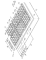
(1)試料分析素子の構造
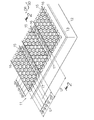
図1は本発明の一実施形態に係る試料分析素子11を概略的に示す。この試料分析素子11すなわちセンサーチップは基板(基体)12を備える。基板12は例えば成型材料から形成される。成型材料には例えば樹脂材が使用されることができる。樹脂材にはポリメタクリル酸メチル樹脂(PMMA樹脂)といったアクリル樹脂が含まれることができる。
(1) Structure of Sample Analysis Element FIG. 1 schematically shows a
基板12の表面には金属膜13が形成される。金属膜13は金属から形成される。金属膜13は例えば銀から形成されることができる。その他、金属には金またはアルミニウムが用いられてもよい。金属膜13は例えば基板12の表面に一面に途切れなく形成されることができる。金属膜13は均一な膜厚で形成されることができる。金属膜13の膜厚は例えば20nm程度に設定されることができる。
A
金属膜13の表面にはナノ構造体15が形成される。ナノ構造体15は金属膜13の表面から突出する。ナノ構造体15は基板12の表面に分散する。個々のナノ構造体15は角柱に形成される。角柱の水平断面すなわち輪郭は例えば正方形に形成される。正方形の一辺の長さは例えば1〜1000nm程度に設定されることができる。角柱の高さ(金属膜13の表面から)は例えば10〜100nm程度で設定されることができる。角柱の水平断面は正方形以外の多角形に形成されてもよい。ナノ構造体15は円柱その他の立体形状に形成されてもよい。
A
ナノ構造体15はナノ構造体群16を形成する。ナノ構造体群16は第1方向(1方向)DRに所定の長ピッチLP(第2のピッチ)で配列される。長ピッチLPの大きさは、後述されるように、エバネッセント波の波数に応じて設定される。ナノ構造体群16同士の間には、ナノ構造体を含まない平面領域(ナノ構造体を含まない領域)17が形成される。すなわち、隣接するナノ構造体群16同士の間はでナノ構造体15の形成は排除される。
The
個々のナノ構造体群16内でナノ構造体15同士は第1方向DRに短ピッチSP(第1のピッチ)で配置される。同時に、個々のナノ構造体群16内でナノ構造体15同士は第1方向DRに交差する第2方向(第2の方向)SDに短ピッチSPで配置される。ここでは、第2方向SDは基板12の表面を含む1仮想平面内で第1方向DRに直交する。したがって、個々のナノ構造体群16内で複数のナノ構造体15は短ピッチSPで格子状に配置される。短ピッチSPは少なくとも長ピッチLPよりも小さく設定される。ナノ構造体群16内では、隣接するナノ構造体15同士の間隔は、隣接するナノ構造体群16同士の間隔すなわち第1方向DRに特定される平面領域17の幅よりも小さく設定される。ここでは、平面領域17の幅は短ピッチSPよりも大きく設定される。すなわち、ナノ構造体群16同士の間隔は短ピッチSPよりも大きく設定される。
Within each
図2に示されるように、個々のナノ構造体15は誘電体の本体18を備える。本体18は基板12の表面から突き出る。本体18は基板12の材料と同一の材料から形成されることができる。本体18は基板12の表面に一体に形成されることができる。
As shown in FIG. 2, each
個々のナノ構造体15では本体18の表面は金属膜19で覆われる。金属膜19は金属膜13と同一の材料から形成されることができる。金属膜19および金属膜13は1枚の膜として形成されることができる。金属膜19は均一な膜厚で形成されることができる。
In each
(2)電場強度の検証
本発明者は試料分析素子11の電場強度を検証した。検証にあたってFDTD(Finite−Difference Time−Domain)法のシミュレーションソフトウェアが利用された。図3(a)および図3(b)に示されるように、本発明者はYee Cellに基づきシュミレーションモデルの単位ユニットを構築した。この単位ユニットでは120nm角のPMMA製基板12に銀の金属膜13が形成された。金属膜13の膜厚は20nmに設定された。PMMA製の本体18の輪郭は40nm角の正方形に設定された。本体18の高さは(基板12の表面から)は60nmに設定された。
(2) Verification of electric field strength The present inventors verified the electric field strength of the
図4(a)に示されるように、第1モデルではx軸方向にナノ構造体群16の長ピッチLPは240nmに設定された。1列の単位ユニットすなわちナノ構造体15で1つのナノ構造体群16が構成された。その結果、ナノ構造体群16同士の間には1列の空隙単位ユニットで平面領域17が形成された。空隙単位ユニットは120nm角の空隙で構成された。先頭のナノ構造体15で電場強度Exが算出された。周辺屈折率ns=1が設定された。直線偏光の入射光が設定された。偏光面はx軸方向に合わせられた。入射光は垂直入射に設定された。ナノ構造体15では上側の4つの頂点に電場が集中した。
As shown in FIG. 4A, in the first model, the long pitch LP of the
図4(b)〜図4(e)に示されるように、第2〜第5モデルではx軸方向にナノ構造体群16の長ピッチLPは360nm、480nm、600nm、720nmにそれぞれ設定された。個々のモデルでは2列、3列、4列および5列の単位ユニットすなわちナノ構造体15で1つのナノ構造体群16が構成された。その結果、個々のモデルごとにナノ構造体群16同士の間に1列の空隙単位ユニットで平面領域17が形成された。空隙単位ユニットは120nm角の空隙で構成された。第1モデルと同様に、個々のモデルごとに先頭のナノ構造体15で電場強度Exが算出された。
As shown in FIGS. 4B to 4E, in the second to fifth models, the long pitch LP of the
図4(f)に示されるように、本発明者は比較モデルを用意した。比較モデルでは平面領域17は省略された。すなわち、ナノ構造体群16は設定されなかった。単純にナノ構造体15が短ピッチSPで格子状に配置された。前述と同様に、選択された1つのナノ構造体15で電場強度Exが算出された。
As shown in FIG. 4F, the present inventor prepared a comparative model. In the comparative model, the
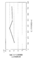
図5は電場強度Exに基づき作成された分散関係を示す。ここでは、単位面積当たりに換算された電場強度Exの二乗和が特定された。二乗和の特定にあたってナノ構造体15の上側の4つの頂点それぞれで電場強度Exが算出された。個々の頂点ごとに電場強度Exの二乗値が算出され、繰り返し計算の最小単位の全ての頂点の二乗値が足し合わせられた。単位面積として比較モデルの面積が設定された。足し合わせられた結果がその単位面積当たりに換算された。こうして単位面積当たり電場強度Exの二乗和が算出された。入射光の波長と二乗和との関係すなわち周波数特性が算出された。1次ピーク(極大値)および2次ピークを示す周波数が特定された。
FIG. 5 shows the dispersion relation created based on the electric field intensity Ex. Here, the sum of squares of the electric field intensity Ex converted per unit area was specified. In specifying the sum of squares, the electric field strength Ex was calculated at each of the four apexes on the upper side of the
図5で波数kは長ピッチLPに応じて特定される。直線21は空気(ns=1.0)の分散関係を示す。空気の分散関係は比例関係を示す。曲線22は屈折率(ns=1.0)の銀Agの伝播表面プラズモン共鳴の分散関係を示す。黒プロットは、長ピッチLPごとにナノ構造体15で電場強度の1次ピーク(極値)を形成する入射光の角周波数ωを示す。第4モデル(LP=600nmp)および比較モデル(図示されず)で角周波数ω=2.88[eV/c]が得られた一方で、第2、第3および第5モデル(LP=360nmp、480nmp、720nmp)で角周波数ω=2.95[eV/c]が得られた。白プロットは、長ピッチLPごとにナノ構造体15で電場強度の2次ピークを形成する入射光の角周波数ωを示す。第2および第4モデル(LP=360nmp、600nmp)で角周波数ω=2.43[eV/c]が得られた一方で、第3モデル(LP=480nmp)で角周波数ω=2.34[eV/c]が得られた。いわゆるAnti−Crossing Behavior(ハイブリッドモードの指標として知られる)は観察されなかった。
In FIG. 5, the wave number k is specified according to the long pitch LP. A
図6は電場強度Exの最大値を示す。比較モデルに対して第2〜第5モデルでは電場強度Exの最大値が増大することが確認された。図7は単位面積当たり電場強度Exの二乗和を示す。比較モデルに対して第2〜第5モデルでは単位面積当たり電場強度Exの二乗和が増大することが確認された。特に、第2モデル(LP=360nmp)では電場強度Exの最大値および単位面積当たり電場強度Exの二乗和ともに大きな値が得られることが確認された。 FIG. 6 shows the maximum value of the electric field intensity Ex. It was confirmed that the maximum value of the electric field intensity Ex increases in the second to fifth models compared to the comparative model. FIG. 7 shows the square sum of the electric field intensity Ex per unit area. In comparison with the comparative model, it was confirmed that the sum of squares of the electric field intensity Ex per unit area increased in the second to fifth models. In particular, in the second model (LP = 360 nmp), it was confirmed that a large value was obtained for both the maximum value of the electric field intensity Ex and the square sum of the electric field intensity Ex per unit area.
ナノ構造体15の金属膜19では入射光の働きで局在表面プラズモン共鳴(LSPR)が誘起される。検証結果から明らかなように、ナノ構造体群16の括りが確立されると、ナノ構造体15が全面にわたって等ピッチで配列される場合に比べて、ナノ構造体15の金属膜19で近接場光は強められることが確認された。いわゆるホットスポットの形成が確認された。しかも、個々のナノ構造体群16内には複数のナノ構造体15が配置されることから、ナノ構造体15単体が伝播表面プラズモン共鳴の波長に対応するピッチで配置される場合に比べてナノ構造体15の面密度は高められる。したがって、ホットスポットの面密度は高められる。特に、長ピッチLPが伝播表面プラズモン共鳴の波長に対応する大きさで規定されると、ナノ構造体15の金属膜19で近接場光は増強されることが確認された。
In the
図8(a)および図8(b)に示されるように、本発明者は第1比較単位ユニットを用意した。第1比較単位ユニットでは120nm角のシリコン(Si)製基板12の表面に銀の金属膜13が形成された。金属膜13の膜厚は20nmに設定された。ナノ構造体15の本体18は二酸化シリコン(SiO2)から形成された。その他の構造は前述の単位ユニットと同様に形成された。
As shown in FIG. 8A and FIG. 8B, the present inventor prepared a first comparison unit unit. In the first comparative unit unit, a
本発明者は同様に第2比較単位ユニットを用意した。第2比較単位ユニットでは120nm角の二酸化シリコン(SiO2)製基板12の表面に銀の金属膜13が形成された。金属膜13の膜厚は20nmに設定された。ナノ構造体15の本体18は二酸化シリコン(SiO2)から形成された。すなわち、ナノ構造体15の本体18と基板12とは一体構造に設定された。その他の構造は前述の単位ユニットと同様に形成された。
The inventor similarly prepared a second comparison unit. In the second comparison unit unit, a
図9は電場強度Exの波長依存性を示す。波長依存性の特定にあたって単位ユニット、第1比較単位ユニットおよび第2比較単位ユニットで比較モデルが構築された。比較モデルで入射光の波長ごとに前述と同様に単位面積当たり電場強度Exの二乗和が算出された。このとき、二酸化シリコンの屈折率は1.45に設定されPMMAの屈折率は1.48に設定された。図9から明らかなように、第1比較単位ユニットでは単位ユニットおよび第2比較単位ユニットに対して電場強度Exの増強が観察された。単位ユニットと第2比較単位ユニットとの間では電場強度Exにほとんど差が観察されなかった。この結果から、第1比較単位ユニットではシリコン製基板12の表面から反射する戻り光の効果で電場強度Exが増大したことが容易に推測されることができる。その一方で、ナノ構造体15の本体18と基板12とが一体に形成されると、ナノ構造体15の本体18と基板12とは同一の材料から形成されることができる。ナノ構造体15の本体18と基板12とは一体成型で形成されることができる。試料分析素子11の製造工程は簡素化されることができる。試料分析素子11の量産性は高められることができる。一体成型の実施にあたってナノ構造体15および基板12は成型材料から形成されればよい。
FIG. 9 shows the wavelength dependence of the electric field intensity Ex. In identifying the wavelength dependence, a comparison model was constructed with the unit unit, the first comparison unit unit, and the second comparison unit unit. In the comparative model, the sum of squares of the electric field intensity Ex per unit area was calculated for each wavelength of incident light in the same manner as described above. At this time, the refractive index of silicon dioxide was set to 1.45, and the refractive index of PMMA was set to 1.48. As is clear from FIG. 9, in the first comparison unit unit, an increase in the electric field intensity Ex was observed with respect to the unit unit and the second comparison unit unit. Almost no difference in electric field intensity Ex was observed between the unit unit and the second comparison unit unit. From this result, in the first comparison unit unit, it can be easily estimated that the electric field intensity Ex has increased due to the effect of the return light reflected from the surface of the
前述のように、金属膜13および金属膜19は1枚の膜として形成されることができる。したがって、金属膜13、19は基板12の表面で一律に形成されれば済む。その結果、試料分析素子11の製造工程は簡素化されることができる。試料分析素子11の量産性は高められることができる。
As described above, the
(3)試料分析素子の製造方法
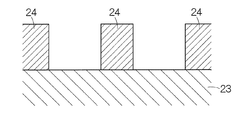
次に、試料分析素子11の製造方法を簡単に説明する。試料分析素子11の製造にあたってスタンパーが製造される。図10に示されるように、シリコン(Si)基板23の表面で二酸化シリコン(SiO2)の突起24が形成される。シリコン基板23の表面は平滑面に形成される。突起24は、基板12の表面に分散するナノ構造体15の本体18を象る。突起24の形成にあたって例えばリソグラフィ技術は用いられることができる。シリコン基板23の表面に一面に二酸化シリコン膜が形成される。二酸化シリコン膜の表面にナノ構造体15の本体18を象ったマスクが形成される。マスクには例えばフォトレジスト膜が用いられればよい。マスクの周囲で二酸化シリコン膜が除去されると、二酸化シリコン膜から個々の突起24は成形される。こうした成形にあたってエッチング処理やミリング処理が実施されればよい。
(3) Method for Manufacturing Sample Analysis Element Next, a method for manufacturing the
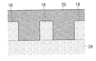
図11に示されるように、シリコン基板23の表面にニッケル(Ni)膜25が形成される。ニッケル膜25の形成にあたって無電解めっきが実施される。続いて、図12に示されるように、ニッケル膜25に基づき電鋳が実施される。シリコン基板23の表面には肉厚のニッケル板26が形成される。その後、図13に示されるように、ニッケル板26はシリコン基板23から剥離される。こうしてニッケル製のスタンパーは製造されることができる。ニッケル板26すなわちスタンパーの表面は平滑面に形成される。平滑面には突起24の剥離痕で窪み27が形成される。
As shown in FIG. 11, a nickel (Ni)
図14に示されるように、基板28は成型される。成型にあたって例えば成型材料の射出成型が利用されることができる。基板28の表面にはナノ構造体15の本体18が一体成型される。図15に示されるように、基板28の表面に一面に金属膜29が形成される。金属膜29の形成にあたって無電解めっきやスパッタリング、蒸着などが用いられることができる。その後、基板28から個々の基板12が切り出される。基板12の表面は金属膜13で覆われる。スタンパーは試料分析素子11の生産性の向上に大いに貢献することができる。
As shown in FIG. 14, the
(4)一実施形態に係る検出装置
図16は一実施形態に係る標的分子検出装置(検出装置)31を概略的に示す。標的分子検出装置31はセンサーユニット32を備える。センサーユニット32には導入通路33と排出通路34とが個別に接続される。導入通路33からセンサーユニット32に気体は導入される。センサーユニット32から排出通路34に気体は排出される。導入通路33の通路入口35にはフィルター36が設置される。フィルター36は例えば気体中の塵埃や水蒸気を除去することができる。排出通路34の通路出口37には吸引ユニット38が設置される。吸引ユニット38は送風ファンで構成される。送風ファンの作動に応じて気体は導入通路33、センサーユニット32および排出通路34を順番に流通する。こうした気体の流通経路内でセンサーユニット32の前後にはシャッター(図示されず)が設置される。シャッターの開閉に応じてセンサーユニット32内に気体は閉じ込められることができる。
(4) Detection Device According to One Embodiment FIG. 16 schematically shows a target molecule detection device (detection device) 31 according to one embodiment. The target
標的分子検出装置31はラマン散乱光検出ユニット41を備える。ラマン散乱光検出ユニット41は、センサーユニット32に照射光を照射しラマン散乱光を検出する。ラマン散乱光検出ユニット41には光源42が組み込まれる。光源42にはレーザー光源が用いられることができる。レーザー光源は特定波長(単一波長)で直線偏光のレーザー光を放射することができる。
The target
ラマン散乱光検出ユニット41は受光素子(光検出器)43を備える。受光素子43は例えば光の強度を検出することができる。受光素子43は光の強度に応じて検出電流を出力することができる。したがって、受光素子43から出力される電流の大きさに応じて光の強度は特定されることができる。
The Raman scattered
光源42とセンサーユニット32との間、および、センサーユニット32と受光素子43との間には光学系44が構築される。光学系44は光源42とセンサーユニット32との間に光路を形成すると同時にセンサーユニット32と受光素子43との間に光路を形成する。光学系44の働きで光源42の光はセンサーユニット32に導かれる。センサーユニット32の反射光は光学系44の働きで受光素子43に導かれる。
An
光学系44はコリメーターレンズ45、ダイクロイックミラー46、対物レンズ47、集光レンズ48、凹レンズ49、光学フィルター51および分光器52を備える。ダイクロイックミラー46は例えばセンサーユニット32と受光素子43との間に配置される。対物レンズ47はダイクロイックミラー46とセンサーユニット32との間に配置される。対物レンズ47はダイクロイックミラー46から供給される平行光を集光してセンサーユニット32に導く。センサーユニット32の反射光は対物レンズ47で平行光に変換されダイクロイックミラー46を透過する。ダイクロイックミラー46と受光素子43との間には集光レンズ48、凹レンズ49、光学フィルター51および分光器52が配置される。対物レンズ47、集光レンズ48および凹レンズ49の光軸は同軸に合わせ込まれる。集光レンズ48で集光された光は凹レンズ49で再び平行光に変換される。光学フィルター51はレイリー散乱光を除去する。ラマン散乱光は光学フィルター51を通過する。分光器52は例えば特定波長の光を選択的に透過させる。こうして受光素子43では特定波長ごとに光の強度が検出される。分光器52には例えばエタロンが用いられることができる。
The
光源42の光軸は対物レンズ47および集光レンズ48の光軸に直交する。ダイクロイックミラー46の表面はこれら光軸に45度の角度で交差する。ダイクロイックミラー46と光源42との間にはコリメーターレンズ45が配置される。こうしてコリメーターレンズ45は光源42に向き合わせられる。コリメーターレンズ45の光軸は光源42の光軸に同軸に合わせ込まれる。
The optical axis of the
標的分子検出装置31は制御ユニット53を備える。制御ユニット53に、光源42、分光器52、受光素子43、吸引ユニット38、その他の機器が接続される。制御ユニット53は、光源42、分光器52および吸引ユニット38の動作を制御するとともに、受光素子43の出力信号を処理する。制御ユニット53には信号コネクター54が接続される。制御ユニット53は信号コネクター54を通じて外部と信号をやりとりすることができる。
The target
標的分子検出装置31は電源ユニット55を備える。電源ユニット55は制御ユニット53に接続される。電源ユニット55は制御ユニット53に動作電力を供給する。制御ユニット53は電源ユニット55から電力の供給を受けて動作することができる。電源ユニット55には例えば1次電池や2次電池が用いられることができる。2次電池は、例えば、充電用の電源コネクター56を有することができる。
The target
制御ユニット53は信号処理制御部を備える。信号処理制御部は例えば中央演算処理装置(CPU)と、RAM(ランダムアクセスメモリー)やROM(リードオンリーメモリー)といった記憶回路で構成されることができる。ROMには例えば処理プログラムやスペクトルデータが格納されることができる。スペクトルデータでは標的分子のラマン散乱光のスペクトルが特定される。CPUは、一時的にRAMに処理プログラムやスペクトルデータを取り込みながら、処理プログラムを実行する。CPUは、スペクトルデータに、分光器および受光素子の働きで特定される光のスペクトルを照らし合わせる。
The
センサーユニット32は試料分析素子11を備える。試料分析素子11は基板58に向き合わせられる。試料分析素子11と基板58との間には気体室59が形成される。気体室59は一端で導入通路33に接続され他端で排出通路34に接続される。気体室59内にナノ構造体群16が配置される。光源42から放出される光はコリメーターレンズ45で平行光に変換される。直線偏光の光はダイクロイックミラー46で反射する。反射した光は対物レンズ47で集光されてセンサーユニット32に照射される。このとき、光は試料分析素子11の表面に直交する垂直方向に入射することができる。いわゆる垂直入射が確立されることができる。光の偏光面は試料分析素子11の第1方向DRに平行に合わせ込まれる。照射された光の働きでナノ構造体15で近接場光は強められる。いわゆるホットスポットが形成される。
The
このとき、ホットスポットでナノ構造体15に標的分子が付着すると、標的分子からレイリー散乱光およびラマン散乱光が生成される。いわゆる表面増強ラマン散乱が実現される。その結果、標的分子の種類に応じたスペクトルで光は対物レンズ47に向かって放出される。
At this time, when the target molecule adheres to the
こうしてセンサーユニット32から放出される光は対物レンズ47で平行光に変換されダイクロイックミラー46、集光レンズ48、凹レンズ49および光学フィルター51を通過する。ラマン散乱光は分光器52に入射する。分光器52はラマン散乱光を分光する。こうして特定の波長ごとに受光素子43は光の強度を検出する。光のスペクトルはスペクトルデータに照らし合わせられる。光のスペクトルに応じて標的分子は検出されることができる。こうして標的分子検出装置31は表面増強ラマン散乱に基づき例えばアデノウィルスやライノウィルス、HIVウィルス、インフルエンザウィルスといった標的物質を検出することができる。
Thus, the light emitted from the
(5)試料分析素子の変形例
図17は変形例に係る試料分析素子11aを概略的に示す。この試料分析素子11aでは、前述の第1方向DRに加えて第2方向SDにナノ構造体群16aは細分化される。すなわち、ナノ構造体群16aは、第1方向DRに所定の長ピッチLPで配列されると同時に、第2方向にSDに所定の長ピッチLPで配列される。こうして第1方向DRに加えて第2方向SDにナノ構造体群16a同士の間にはナノ構造体を含まない平面領域(金属ナノ体を含まない領域)17が形成される。その他、変形例に係る試料分析素子11aの構成は前述の試料分析素子11と同様である。図中、前述の試料分析素子11と均等な構成や構造には同一の参照符号が付され、その詳細な説明は割愛される。
(5) Modified Example of Sample Analyzing Element FIG. 17 schematically shows a
こうした試料分析素子11aでは、円偏光の入射光が照射されると、個々のナノ構造体15の金属膜19で局在表面プラズモン共鳴が誘起される。第1方向DRの括りに加えて第2方向SDの括りに基づき局在表面プラズモン共鳴は増強される。ナノ構造体15の金属膜19で近接場光は強められる。いわゆるホットスポットが形成される。しかも、個々のナノ構造体群16a内には複数のナノ構造体15が配置されることから、ナノ構造体15の面密度は高められる。したがって、ホットスポットの面密度は高められる。なお、こうした試料分析素子11aが標的分子検出装置31に組み込まれる場合には、光源42は円偏光の光を放出すればよい。
In such a
なお、上記のように本実施形態について詳細に説明したが、本発明の新規事項および効果から実体的に逸脱しない多くの変形が可能であることは当業者には容易に理解できるであろう。したがって、このような変形例はすべて本発明の範囲に含まれる。例えば、明細書または図面において、少なくとも一度、より広義または同義な異なる用語とともに記載された用語は、明細書または図面のいかなる箇所においても、その異なる用語に置き換えられることができる。また、試料分析素子11、11aや標的分子検出装置31等の構成および動作も本実施形態で説明したものに限定されず、種々の変形が可能である。
Although the present embodiment has been described in detail as described above, it will be easily understood by those skilled in the art that many modifications can be made without departing from the novel matters and effects of the present invention. Therefore, all such modifications are included in the scope of the present invention. For example, a term described with a different term having a broader meaning or the same meaning at least once in the specification or the drawings can be replaced with the different term in any part of the specification or the drawings. Further, the configurations and operations of the
11 試料分析素子、12 基体(基板)、13 金属膜、15 ナノ構造体、16 ナノ構造体群、17 ナノ構造体を含まない領域(平面領域)、18 誘電体(本体)、19 金属膜、31 検出装置(標的分子検出装置)、42 光源、43 光検出器(受光素子)、DR 一方向(第1方向)、SD 第2の方向(第2方向)、SP 第1のピッチ(短ピッチ)、LP 第2のピッチ(長ピッチ)。
DESCRIPTION OF
Claims (9)
入射光の波長よりも小さい第1のピッチで前記基体の表面に分散するナノ構造体を含む複数のナノ構造体群とを備え、
前記ナノ構造体では金属膜が誘電体を被覆し、
前記ナノ構造体群は、第1のピッチよりも大きい第2のピッチで1方向に配列されることを特徴とする試料分析素子。 A substrate;
A plurality of nanostructure groups including nanostructures dispersed on the surface of the substrate at a first pitch smaller than the wavelength of incident light,
In the nanostructure, a metal film covers a dielectric,
The sample analysis element, wherein the nanostructure group is arranged in one direction at a second pitch larger than the first pitch.
前記ナノ構造体群に向けて光を放出する光源と、
前記光の照射に応じて前記ナノ構造体群から放射される光を検出する光検出器と
を備えることを特徴とする検出装置。 The sample analysis element according to any one of claims 1 to 8,
A light source that emits light toward the group of nanostructures;
And a photodetector that detects light emitted from the nanostructure group in response to the irradiation of the light.
Priority Applications (3)
| Application Number | Priority Date | Filing Date | Title |
|---|---|---|---|
| JP2012101021A JP2013228303A (en) | 2012-04-26 | 2012-04-26 | Sample analysis element and detector |
| US14/396,608 US20150109619A1 (en) | 2012-04-26 | 2013-04-12 | Sample analysis element and detection device |
| PCT/JP2013/002504 WO2013161210A1 (en) | 2012-04-26 | 2013-04-12 | Sample analysis element and detection device |
Applications Claiming Priority (1)
| Application Number | Priority Date | Filing Date | Title |
|---|---|---|---|
| JP2012101021A JP2013228303A (en) | 2012-04-26 | 2012-04-26 | Sample analysis element and detector |
Publications (2)
| Publication Number | Publication Date |
|---|---|
| JP2013228303A true JP2013228303A (en) | 2013-11-07 |
| JP2013228303A5 JP2013228303A5 (en) | 2015-06-18 |
Family
ID=49482561
Family Applications (1)
| Application Number | Title | Priority Date | Filing Date |
|---|---|---|---|
| JP2012101021A Withdrawn JP2013228303A (en) | 2012-04-26 | 2012-04-26 | Sample analysis element and detector |
Country Status (3)
| Country | Link |
|---|---|
| US (1) | US20150109619A1 (en) |
| JP (1) | JP2013228303A (en) |
| WO (1) | WO2013161210A1 (en) |
Families Citing this family (4)
| Publication number | Priority date | Publication date | Assignee | Title |
|---|---|---|---|---|
| LT6112B (en) * | 2013-05-24 | 2015-01-26 | Integrated Optics, Uab | Active surface raman scater sensor and production method |
| JP6613736B2 (en) * | 2015-09-07 | 2019-12-04 | セイコーエプソン株式会社 | Substance detection method and substance detection apparatus |
| CN113225845A (en) * | 2020-01-21 | 2021-08-06 | 华硕电脑股份有限公司 | Method and apparatus for handling sidelink discontinuous reception with respect to periodic transmissions |
| US11959859B2 (en) | 2021-06-02 | 2024-04-16 | Edwin Thomas Carlen | Multi-gas detection system and method |
Citations (3)
| Publication number | Priority date | Publication date | Assignee | Title |
|---|---|---|---|---|
| JP2009085724A (en) * | 2007-09-28 | 2009-04-23 | Canon Inc | Target substance detector and target substance detecting method |
| JP2009115492A (en) * | 2007-11-02 | 2009-05-28 | Canon Inc | Chemical sensor element, sensing device, and sensing method |
| JP2010256161A (en) * | 2009-04-24 | 2010-11-11 | Konica Minolta Holdings Inc | Plasmon excitation sensor, and assay method using the same |
Family Cites Families (9)
| Publication number | Priority date | Publication date | Assignee | Title |
|---|---|---|---|---|
| JP4156567B2 (en) * | 2004-06-16 | 2008-09-24 | 日本電信電話株式会社 | SPR sensor and refractive index measuring method |
| US7705280B2 (en) * | 2006-07-25 | 2010-04-27 | The Board Of Trustees Of The University Of Illinois | Multispectral plasmonic crystal sensors |
| US20080280374A1 (en) * | 2007-05-08 | 2008-11-13 | General Electric Company | Methods and systems for detecting biological and chemical materials on a submicron structured substrate |
| US20100126567A1 (en) * | 2008-11-21 | 2010-05-27 | Lightwave Power, Inc. | Surface plasmon energy conversion device |
| US20120081703A1 (en) * | 2009-05-07 | 2012-04-05 | Nant Holdings Ip, Llc | Highly Efficient Plamonic Devices, Molecule Detection Systems, and Methods of Making the Same |
| US8767282B2 (en) * | 2009-11-06 | 2014-07-01 | Sharp Laboratories Of America, Inc. | Plasmonic in-cell polarizer |
| US8786852B2 (en) * | 2009-12-02 | 2014-07-22 | Lawrence Livermore National Security, Llc | Nanoscale array structures suitable for surface enhanced raman scattering and methods related thereto |
| US8711356B2 (en) * | 2010-02-25 | 2014-04-29 | Stichting Imec Nederland | Gas sensor with a porous layer that detectably affects a surface lattice resonant condition of a nanoparticle array |
| WO2012149082A2 (en) * | 2011-04-26 | 2012-11-01 | The Government Of The United States Of America, As Represented By The Secretary Of The Navy | Three-dimensional coherent plasmonic nanowire arrays for enhancement of optical processes |
-
2012
- 2012-04-26 JP JP2012101021A patent/JP2013228303A/en not_active Withdrawn
-
2013
- 2013-04-12 WO PCT/JP2013/002504 patent/WO2013161210A1/en active Application Filing
- 2013-04-12 US US14/396,608 patent/US20150109619A1/en not_active Abandoned
Patent Citations (3)
| Publication number | Priority date | Publication date | Assignee | Title |
|---|---|---|---|---|
| JP2009085724A (en) * | 2007-09-28 | 2009-04-23 | Canon Inc | Target substance detector and target substance detecting method |
| JP2009115492A (en) * | 2007-11-02 | 2009-05-28 | Canon Inc | Chemical sensor element, sensing device, and sensing method |
| JP2010256161A (en) * | 2009-04-24 | 2010-11-11 | Konica Minolta Holdings Inc | Plasmon excitation sensor, and assay method using the same |
Also Published As
| Publication number | Publication date |
|---|---|
| WO2013161210A1 (en) | 2013-10-31 |
| US20150109619A1 (en) | 2015-04-23 |
Similar Documents
| Publication | Publication Date | Title |
|---|---|---|
| WO2013157233A1 (en) | Sample analysis element and detection device | |
| JP7199224B2 (en) | Near-field focusing with a hollow nanojet lens | |
| JP5821511B2 (en) | Optical device and detection apparatus | |
| JP5923992B2 (en) | Sample analysis element and detection apparatus | |
| WO2013168404A1 (en) | Sample analyzing element and testing device and sensor cartridge | |
| CN105899983B (en) | Guided mode resonance device | |
| JP2013234941A (en) | Sensor chip, sensor cartridge, and detector | |
| Coenen et al. | Optical properties of single plasmonic holes probed with local electron beam excitation | |
| US9488583B2 (en) | Molecular analysis device | |
| WO2013161210A1 (en) | Sample analysis element and detection device | |
| JP5640592B2 (en) | Optical device unit and detection apparatus | |
| JP2019512743A (en) | Annular nano jet lens | |
| CN102419320A (en) | Detection apparatus | |
| JP5880064B2 (en) | Sample analysis element and detection apparatus | |
| Tagliabue et al. | Facile multifunctional plasmonic sunlight harvesting with tapered triangle nanopatterning of thin films | |
| CN102401794A (en) | Optical device unit and detection apparatus | |
| JP4843543B2 (en) | Fluorescence detection apparatus and method | |
| US10989867B2 (en) | Microsphere based patterning of metal optic/plasmonic sensors including fiber based sensors | |
| TWI647448B (en) | Lens array-based illumination for wafer inspection | |
| JP2013190376A (en) | Sensor chip and method of manufacturing the same, and detector | |
| Trautmann et al. | Plasmon response evaluation based on image-derived arbitrary nanostructures | |
| JP5796395B2 (en) | Optical device, detection apparatus, and detection method | |
| WO2013130027A1 (en) | Light absorption and filtering properties of vertically oriented semiconductor nano wires | |
| CN101217062A (en) | A metal film and its making method | |
| JP2007071615A (en) | Surface plasmon resonance angle spectrum measuring device |
Legal Events
| Date | Code | Title | Description |
|---|---|---|---|
| A521 | Written amendment |
Free format text: JAPANESE INTERMEDIATE CODE: A523 Effective date: 20150424 |
|
| A621 | Written request for application examination |
Free format text: JAPANESE INTERMEDIATE CODE: A621 Effective date: 20150424 |
|
| A131 | Notification of reasons for refusal |
Free format text: JAPANESE INTERMEDIATE CODE: A131 Effective date: 20160209 |
|
| A761 | Written withdrawal of application |
Free format text: JAPANESE INTERMEDIATE CODE: A761 Effective date: 20160408 |