JP2013222856A5 - - Google Patents
Download PDFInfo
- Publication number
- JP2013222856A5 JP2013222856A5 JP2012094114A JP2012094114A JP2013222856A5 JP 2013222856 A5 JP2013222856 A5 JP 2013222856A5 JP 2012094114 A JP2012094114 A JP 2012094114A JP 2012094114 A JP2012094114 A JP 2012094114A JP 2013222856 A5 JP2013222856 A5 JP 2013222856A5
- Authority
- JP
- Japan
- Prior art keywords
- polishing
- wafer
- film thickness
- slurry
- predetermined
- Prior art date
- Legal status (The legal status is an assumption and is not a legal conclusion. Google has not performed a legal analysis and makes no representation as to the accuracy of the status listed.)
- Pending
Links
Images
Description
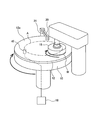
次に、ウェハの膜厚に基づいてウェハの研磨終点を決定する一実施形態について図3のフローチャートを参照して説明する。
ステップ1では、スラリー供給機構30から研磨パッド12に研磨液(スラリー)を供給しながら、ウェハを所定の研磨時間だけ研磨する。この所定の研磨時間は、目標膜厚に達しない範囲で長く設定することが好ましい。
Next, an embodiment for determining the polishing end point of the wafer based on the film thickness of the wafer will be described with reference to the flowchart of FIG.
In step 1, the wafer is polished for a predetermined polishing time while supplying a polishing liquid (slurry) from the
Priority Applications (4)
| Application Number | Priority Date | Filing Date | Title |
|---|---|---|---|
| JP2012094114A JP2013222856A (en) | 2012-04-17 | 2012-04-17 | Polishing device and polishing method |
| KR1020130039204A KR20130117334A (en) | 2012-04-17 | 2013-04-10 | Polishing apparatus and polishing method |
| TW102113034A TW201343324A (en) | 2012-04-17 | 2013-04-12 | Polishing apparatus and polishing method |
| US13/864,181 US20130273814A1 (en) | 2012-04-17 | 2013-04-16 | Polishing apparatus and polishing method |
Applications Claiming Priority (1)
| Application Number | Priority Date | Filing Date | Title |
|---|---|---|---|
| JP2012094114A JP2013222856A (en) | 2012-04-17 | 2012-04-17 | Polishing device and polishing method |
Publications (2)
| Publication Number | Publication Date |
|---|---|
| JP2013222856A JP2013222856A (en) | 2013-10-28 |
| JP2013222856A5 true JP2013222856A5 (en) | 2014-10-23 |
Family
ID=49325509
Family Applications (1)
| Application Number | Title | Priority Date | Filing Date |
|---|---|---|---|
| JP2012094114A Pending JP2013222856A (en) | 2012-04-17 | 2012-04-17 | Polishing device and polishing method |
Country Status (4)
| Country | Link |
|---|---|
| US (1) | US20130273814A1 (en) |
| JP (1) | JP2013222856A (en) |
| KR (1) | KR20130117334A (en) |
| TW (1) | TW201343324A (en) |
Families Citing this family (10)
| Publication number | Priority date | Publication date | Assignee | Title |
|---|---|---|---|---|
| KR102326730B1 (en) * | 2014-03-12 | 2021-11-17 | 가부시키가이샤 에바라 세이사꾸쇼 | Correction method of film thickness measurement value, film thickness corrector and eddy current sensor |
| JP6595987B2 (en) * | 2014-04-22 | 2019-10-23 | 株式会社荏原製作所 | Polishing method |
| JP6404172B2 (en) | 2015-04-08 | 2018-10-10 | 株式会社荏原製作所 | Film thickness measuring method, film thickness measuring apparatus, polishing method, and polishing apparatus |
| KR102313560B1 (en) * | 2015-06-02 | 2021-10-18 | 주식회사 케이씨텍 | Chemical mechanical polishing apparatus |
| JP2018083267A (en) * | 2016-11-25 | 2018-05-31 | 株式会社荏原製作所 | Polishing device and polishing method |
| JP6829653B2 (en) * | 2017-05-17 | 2021-02-10 | 株式会社荏原製作所 | Polishing equipment and polishing method |
| JP6948868B2 (en) | 2017-07-24 | 2021-10-13 | 株式会社荏原製作所 | Polishing equipment and polishing method |
| JP7083279B2 (en) * | 2018-06-22 | 2022-06-10 | 株式会社荏原製作所 | How to identify the trajectory of the eddy current sensor, how to calculate the progress of polishing the substrate, how to stop the operation of the substrate polishing device and how to equalize the progress of polishing the substrate, to execute these methods. The program and the non-transient recording medium on which the program is recorded |
| JP7316785B2 (en) * | 2018-12-26 | 2023-07-28 | 株式会社荏原製作所 | How to clean the optical film thickness measurement system |
| JP7341022B2 (en) | 2019-10-03 | 2023-09-08 | 株式会社荏原製作所 | Substrate polishing equipment and film thickness map creation method |
Family Cites Families (11)
| Publication number | Priority date | Publication date | Assignee | Title |
|---|---|---|---|---|
| JP4011892B2 (en) * | 2001-11-20 | 2007-11-21 | 富士通株式会社 | Polishing equipment |
| US20040242121A1 (en) * | 2003-05-16 | 2004-12-02 | Kazuto Hirokawa | Substrate polishing apparatus |
| JP4451111B2 (en) * | 2003-10-20 | 2010-04-14 | 株式会社荏原製作所 | Eddy current sensor |
| JP4641395B2 (en) * | 2004-08-17 | 2011-03-02 | Okiセミコンダクタ株式会社 | Semiconductor device grinding method and grinding apparatus |
| US8246417B2 (en) * | 2006-09-12 | 2012-08-21 | Ebara Corporation | Polishing apparatus and polishing method |
| KR101381341B1 (en) * | 2006-10-06 | 2014-04-04 | 가부시끼가이샤 도시바 | Processing end point detection method, polishing method, and polishing apparatus |
| JP5080933B2 (en) * | 2007-10-18 | 2012-11-21 | 株式会社荏原製作所 | Polishing monitoring method and polishing apparatus |
| JP2009158749A (en) * | 2007-12-27 | 2009-07-16 | Ricoh Co Ltd | Chemical mechanical polishing method and chemical mechanical polishing apparatus |
| JP5513795B2 (en) * | 2009-07-16 | 2014-06-04 | 株式会社荏原製作所 | Polishing method and apparatus |
| JP5728239B2 (en) * | 2010-03-02 | 2015-06-03 | 株式会社荏原製作所 | Polishing monitoring method, polishing method, polishing monitoring apparatus, and polishing apparatus |
| JP5980476B2 (en) * | 2010-12-27 | 2016-08-31 | 株式会社荏原製作所 | Polishing apparatus and polishing method |
-
2012
- 2012-04-17 JP JP2012094114A patent/JP2013222856A/en active Pending
-
2013
- 2013-04-10 KR KR1020130039204A patent/KR20130117334A/en not_active Application Discontinuation
- 2013-04-12 TW TW102113034A patent/TW201343324A/en unknown
- 2013-04-16 US US13/864,181 patent/US20130273814A1/en not_active Abandoned
Similar Documents
| Publication | Publication Date | Title |
|---|---|---|
| JP2013222856A5 (en) | ||
| CR20130639A (en) | SYSTEMS AND METHODS BASED ON OPTICAL AND PRESSURE COHERENCE TOMOGRAPHY | |
| JP2012023289A5 (en) | ||
| EP3062337A4 (en) | Polishing liquid composition for silicon wafers | |
| JP2012222330A5 (en) | ||
| JP2017005051A5 (en) | ||
| EP3007213A4 (en) | Composition for silicon wafer polishing | |
| EP2997104A4 (en) | Use of a chemical-mechanical polishing (cmp) composition for polishing a substrate or layer containing at least one iii-v material | |
| TWD164675S (en) | Beverage machine | |
| TWD172620S (en) | Portion of a charger for portable electronic device | |
| JP2015517923A5 (en) | ||
| JP2012033615A5 (en) | ||
| DK2307612T3 (en) | FLEXIBLE, FLAT SUBSTRATES WITH AN ABRASIVE SURFACE | |
| JP2014233757A5 (en) | ||
| SG11201600902WA (en) | Slurry, polishing-liquid set, polishing liquid, method for polishing substrate, and substrate | |
| EP2981392A4 (en) | Pad for supporting abrasive disc | |
| JP2012101354A5 (en) | ||
| TWD166339S (en) | Portion of a note dispenser | |
| JP2013531183A5 (en) | ||
| JP2015070207A5 (en) | Optical semiconductor device | |
| JP2013115210A5 (en) | Bonding device | |
| JP2012146382A5 (en) | ||
| TWD169006S (en) | Wafer holder for manufacturing semiconductor | |
| TWD159877S (en) | Parts of a soap dish | |
| TWD167111S (en) | Elastic membrane for semiconductor wafer polishing apparatus |