JP2013218126A - Display device - Google Patents
Display device Download PDFInfo
- Publication number
- JP2013218126A JP2013218126A JP2012088871A JP2012088871A JP2013218126A JP 2013218126 A JP2013218126 A JP 2013218126A JP 2012088871 A JP2012088871 A JP 2012088871A JP 2012088871 A JP2012088871 A JP 2012088871A JP 2013218126 A JP2013218126 A JP 2013218126A
- Authority
- JP
- Japan
- Prior art keywords
- terminal
- terminals
- dummy
- outermost
- display device
- Prior art date
- Legal status (The legal status is an assumption and is not a legal conclusion. Google has not performed a legal analysis and makes no representation as to the accuracy of the status listed.)
- Pending
Links
Images


Classifications
-
- H—ELECTRICITY
- H01—ELECTRIC ELEMENTS
- H01L—SEMICONDUCTOR DEVICES NOT COVERED BY CLASS H10
- H01L25/00—Assemblies consisting of a plurality of individual semiconductor or other solid state devices ; Multistep manufacturing processes thereof
- H01L25/18—Assemblies consisting of a plurality of individual semiconductor or other solid state devices ; Multistep manufacturing processes thereof the devices being of types provided for in two or more different subgroups of the same main group of groups H01L27/00 - H01L33/00, or in a single subclass of H10K, H10N
-
- G—PHYSICS
- G02—OPTICS
- G02F—OPTICAL DEVICES OR ARRANGEMENTS FOR THE CONTROL OF LIGHT BY MODIFICATION OF THE OPTICAL PROPERTIES OF THE MEDIA OF THE ELEMENTS INVOLVED THEREIN; NON-LINEAR OPTICS; FREQUENCY-CHANGING OF LIGHT; OPTICAL LOGIC ELEMENTS; OPTICAL ANALOGUE/DIGITAL CONVERTERS
- G02F1/00—Devices or arrangements for the control of the intensity, colour, phase, polarisation or direction of light arriving from an independent light source, e.g. switching, gating or modulating; Non-linear optics
- G02F1/01—Devices or arrangements for the control of the intensity, colour, phase, polarisation or direction of light arriving from an independent light source, e.g. switching, gating or modulating; Non-linear optics for the control of the intensity, phase, polarisation or colour
- G02F1/13—Devices or arrangements for the control of the intensity, colour, phase, polarisation or direction of light arriving from an independent light source, e.g. switching, gating or modulating; Non-linear optics for the control of the intensity, phase, polarisation or colour based on liquid crystals, e.g. single liquid crystal display cells
- G02F1/133—Constructional arrangements; Operation of liquid crystal cells; Circuit arrangements
- G02F1/1333—Constructional arrangements; Manufacturing methods
- G02F1/1345—Conductors connecting electrodes to cell terminals
- G02F1/13454—Drivers integrated on the active matrix substrate
-
- G—PHYSICS
- G02—OPTICS
- G02F—OPTICAL DEVICES OR ARRANGEMENTS FOR THE CONTROL OF LIGHT BY MODIFICATION OF THE OPTICAL PROPERTIES OF THE MEDIA OF THE ELEMENTS INVOLVED THEREIN; NON-LINEAR OPTICS; FREQUENCY-CHANGING OF LIGHT; OPTICAL LOGIC ELEMENTS; OPTICAL ANALOGUE/DIGITAL CONVERTERS
- G02F1/00—Devices or arrangements for the control of the intensity, colour, phase, polarisation or direction of light arriving from an independent light source, e.g. switching, gating or modulating; Non-linear optics
- G02F1/01—Devices or arrangements for the control of the intensity, colour, phase, polarisation or direction of light arriving from an independent light source, e.g. switching, gating or modulating; Non-linear optics for the control of the intensity, phase, polarisation or colour
- G02F1/13—Devices or arrangements for the control of the intensity, colour, phase, polarisation or direction of light arriving from an independent light source, e.g. switching, gating or modulating; Non-linear optics for the control of the intensity, phase, polarisation or colour based on liquid crystals, e.g. single liquid crystal display cells
- G02F1/133—Constructional arrangements; Operation of liquid crystal cells; Circuit arrangements
- G02F1/1333—Constructional arrangements; Manufacturing methods
- G02F1/1345—Conductors connecting electrodes to cell terminals
- G02F1/13458—Terminal pads
-
- G—PHYSICS
- G02—OPTICS
- G02F—OPTICAL DEVICES OR ARRANGEMENTS FOR THE CONTROL OF LIGHT BY MODIFICATION OF THE OPTICAL PROPERTIES OF THE MEDIA OF THE ELEMENTS INVOLVED THEREIN; NON-LINEAR OPTICS; FREQUENCY-CHANGING OF LIGHT; OPTICAL LOGIC ELEMENTS; OPTICAL ANALOGUE/DIGITAL CONVERTERS
- G02F1/00—Devices or arrangements for the control of the intensity, colour, phase, polarisation or direction of light arriving from an independent light source, e.g. switching, gating or modulating; Non-linear optics
- G02F1/01—Devices or arrangements for the control of the intensity, colour, phase, polarisation or direction of light arriving from an independent light source, e.g. switching, gating or modulating; Non-linear optics for the control of the intensity, phase, polarisation or colour
- G02F1/13—Devices or arrangements for the control of the intensity, colour, phase, polarisation or direction of light arriving from an independent light source, e.g. switching, gating or modulating; Non-linear optics for the control of the intensity, phase, polarisation or colour based on liquid crystals, e.g. single liquid crystal display cells
- G02F1/133—Constructional arrangements; Operation of liquid crystal cells; Circuit arrangements
- G02F1/136—Liquid crystal cells structurally associated with a semi-conducting layer or substrate, e.g. cells forming part of an integrated circuit
- G02F1/1362—Active matrix addressed cells
- G02F1/1368—Active matrix addressed cells in which the switching element is a three-electrode device
-
- H—ELECTRICITY
- H01—ELECTRIC ELEMENTS
- H01L—SEMICONDUCTOR DEVICES NOT COVERED BY CLASS H10
- H01L23/00—Details of semiconductor or other solid state devices
- H01L23/52—Arrangements for conducting electric current within the device in operation from one component to another, i.e. interconnections, e.g. wires, lead frames
- H01L23/522—Arrangements for conducting electric current within the device in operation from one component to another, i.e. interconnections, e.g. wires, lead frames including external interconnections consisting of a multilayer structure of conductive and insulating layers inseparably formed on the semiconductor body
- H01L23/5226—Via connections in a multilevel interconnection structure
-
- H—ELECTRICITY
- H01—ELECTRIC ELEMENTS
- H01L—SEMICONDUCTOR DEVICES NOT COVERED BY CLASS H10
- H01L23/00—Details of semiconductor or other solid state devices
- H01L23/52—Arrangements for conducting electric current within the device in operation from one component to another, i.e. interconnections, e.g. wires, lead frames
- H01L23/522—Arrangements for conducting electric current within the device in operation from one component to another, i.e. interconnections, e.g. wires, lead frames including external interconnections consisting of a multilayer structure of conductive and insulating layers inseparably formed on the semiconductor body
- H01L23/532—Arrangements for conducting electric current within the device in operation from one component to another, i.e. interconnections, e.g. wires, lead frames including external interconnections consisting of a multilayer structure of conductive and insulating layers inseparably formed on the semiconductor body characterised by the materials
- H01L23/53204—Conductive materials
- H01L23/53209—Conductive materials based on metals, e.g. alloys, metal silicides
-
- H—ELECTRICITY
- H01—ELECTRIC ELEMENTS
- H01L—SEMICONDUCTOR DEVICES NOT COVERED BY CLASS H10
- H01L27/00—Devices consisting of a plurality of semiconductor or other solid-state components formed in or on a common substrate
- H01L27/02—Devices consisting of a plurality of semiconductor or other solid-state components formed in or on a common substrate including semiconductor components specially adapted for rectifying, oscillating, amplifying or switching and having at least one potential-jump barrier or surface barrier; including integrated passive circuit elements with at least one potential-jump barrier or surface barrier
- H01L27/12—Devices consisting of a plurality of semiconductor or other solid-state components formed in or on a common substrate including semiconductor components specially adapted for rectifying, oscillating, amplifying or switching and having at least one potential-jump barrier or surface barrier; including integrated passive circuit elements with at least one potential-jump barrier or surface barrier the substrate being other than a semiconductor body, e.g. an insulating body
- H01L27/1214—Devices consisting of a plurality of semiconductor or other solid-state components formed in or on a common substrate including semiconductor components specially adapted for rectifying, oscillating, amplifying or switching and having at least one potential-jump barrier or surface barrier; including integrated passive circuit elements with at least one potential-jump barrier or surface barrier the substrate being other than a semiconductor body, e.g. an insulating body comprising a plurality of TFTs formed on a non-semiconducting substrate, e.g. driving circuits for AMLCDs
- H01L27/124—Devices consisting of a plurality of semiconductor or other solid-state components formed in or on a common substrate including semiconductor components specially adapted for rectifying, oscillating, amplifying or switching and having at least one potential-jump barrier or surface barrier; including integrated passive circuit elements with at least one potential-jump barrier or surface barrier the substrate being other than a semiconductor body, e.g. an insulating body comprising a plurality of TFTs formed on a non-semiconducting substrate, e.g. driving circuits for AMLCDs with a particular composition, shape or layout of the wiring layers specially adapted to the circuit arrangement, e.g. scanning lines in LCD pixel circuits
-
- H—ELECTRICITY
- H01—ELECTRIC ELEMENTS
- H01L—SEMICONDUCTOR DEVICES NOT COVERED BY CLASS H10
- H01L33/00—Semiconductor devices with at least one potential-jump barrier or surface barrier specially adapted for light emission; Processes or apparatus specially adapted for the manufacture or treatment thereof or of parts thereof; Details thereof
- H01L33/02—Semiconductor devices with at least one potential-jump barrier or surface barrier specially adapted for light emission; Processes or apparatus specially adapted for the manufacture or treatment thereof or of parts thereof; Details thereof characterised by the semiconductor bodies
- H01L33/08—Semiconductor devices with at least one potential-jump barrier or surface barrier specially adapted for light emission; Processes or apparatus specially adapted for the manufacture or treatment thereof or of parts thereof; Details thereof characterised by the semiconductor bodies with a plurality of light emitting regions, e.g. laterally discontinuous light emitting layer or photoluminescent region integrated within the semiconductor body
-
- H—ELECTRICITY
- H10—SEMICONDUCTOR DEVICES; ELECTRIC SOLID-STATE DEVICES NOT OTHERWISE PROVIDED FOR
- H10K—ORGANIC ELECTRIC SOLID-STATE DEVICES
- H10K59/00—Integrated devices, or assemblies of multiple devices, comprising at least one organic light-emitting element covered by group H10K50/00
- H10K59/80—Constructional details
- H10K59/88—Dummy elements, i.e. elements having non-functional features
-
- H—ELECTRICITY
- H01—ELECTRIC ELEMENTS
- H01L—SEMICONDUCTOR DEVICES NOT COVERED BY CLASS H10
- H01L2224/00—Indexing scheme for arrangements for connecting or disconnecting semiconductor or solid-state bodies and methods related thereto as covered by H01L24/00
- H01L2224/73—Means for bonding being of different types provided for in two or more of groups H01L2224/10, H01L2224/18, H01L2224/26, H01L2224/34, H01L2224/42, H01L2224/50, H01L2224/63, H01L2224/71
- H01L2224/732—Location after the connecting process
- H01L2224/73201—Location after the connecting process on the same surface
- H01L2224/73203—Bump and layer connectors
- H01L2224/73204—Bump and layer connectors the bump connector being embedded into the layer connector
-
- H—ELECTRICITY
- H05—ELECTRIC TECHNIQUES NOT OTHERWISE PROVIDED FOR
- H05K—PRINTED CIRCUITS; CASINGS OR CONSTRUCTIONAL DETAILS OF ELECTRIC APPARATUS; MANUFACTURE OF ASSEMBLAGES OF ELECTRICAL COMPONENTS
- H05K1/00—Printed circuits
- H05K1/02—Details
- H05K1/11—Printed elements for providing electric connections to or between printed circuits
- H05K1/111—Pads for surface mounting, e.g. lay-out
-
- H—ELECTRICITY
- H05—ELECTRIC TECHNIQUES NOT OTHERWISE PROVIDED FOR
- H05K—PRINTED CIRCUITS; CASINGS OR CONSTRUCTIONAL DETAILS OF ELECTRIC APPARATUS; MANUFACTURE OF ASSEMBLAGES OF ELECTRICAL COMPONENTS
- H05K2201/00—Indexing scheme relating to printed circuits covered by H05K1/00
- H05K2201/09—Shape and layout
- H05K2201/09209—Shape and layout details of conductors
- H05K2201/09654—Shape and layout details of conductors covering at least two types of conductors provided for in H05K2201/09218 - H05K2201/095
- H05K2201/09781—Dummy conductors, i.e. not used for normal transport of current; Dummy electrodes of components
Abstract
Description
本発明は、ICドライバをCOG(Chip On Glass)によって接続する場合の、接続の信頼性を向上させた表示装置に関する。 The present invention relates to a display device with improved connection reliability when an IC driver is connected by COG (Chip On Glass).
液晶表示装置では画素電極および薄膜トランジスタ(TFT)等がマトリクス状に形成されたTFT基板と、TFT基板に対向して、TFT基板の画素電極と対応する場所にブラックマトリクスあるいはオーバーコート膜等が形成された対向基板が設置され、TFT基板と対向基板の間に液晶が挟持されている。そして液晶分子による光の透過率を画素毎に制御することによって画像を形成している。 In a liquid crystal display device, a TFT substrate in which pixel electrodes and thin film transistors (TFTs) are formed in a matrix form, and a black matrix or an overcoat film, etc. are formed at a location corresponding to the pixel electrodes on the TFT substrate, facing the TFT substrate. A counter substrate is installed, and a liquid crystal is sandwiched between the TFT substrate and the counter substrate. An image is formed by controlling the light transmittance of the liquid crystal molecules for each pixel.
液晶表示装置はフラットで軽量であることから、TV等の大型表示装置から、携帯電話やDSC(Digital Still Camera)等、色々な分野で用途が広がっている。液晶表示パネルに外部から電力や信号を供給するために、TFT基板の端子部にフレキシブル配線基板を接続している。また、小型の液晶表示装置においては、ICドライバをCOGによってTFT基板に直接接続することが行われている。そして、フレキシブル配線基板をTFT基板に接続する場合も、ICドライバをCOGによってTFT基板に接続する場合も、ASC(Anisotropic Conductive Film)が用いられることが多い。ASCは樹脂フィルム中に導電性の粒子を有し、この導電性粒子がTFT基板に形成された端子部とフレキシブル配線基板、あるいは、ICドライバとの導通を取っている。 Since the liquid crystal display device is flat and lightweight, the application is expanding in various fields such as a large display device such as a TV, a mobile phone, and a DSC (Digital Still Camera). In order to supply power and signals from the outside to the liquid crystal display panel, a flexible wiring substrate is connected to the terminal portion of the TFT substrate. In a small liquid crystal display device, an IC driver is directly connected to a TFT substrate by COG. In both cases where the flexible wiring substrate is connected to the TFT substrate and the IC driver is connected to the TFT substrate by COG, ASC (Anisotropic Conductive Film) is often used. The ASC has conductive particles in a resin film, and the conductive particles are connected to a terminal portion formed on the TFT substrate and a flexible wiring substrate or an IC driver.
端子は、表示領域から延在してきたゲート線あるいはドレイン線の部分において、保護膜であるゲート絶縁膜あるいはパッシベーション膜にスルーホールを形成し、その部分を導電性金属酸化物によって覆うことによって形成されている。「特許文献1」には、端子のスルーホールとスルーホールとの間に導電性ビーズが存在する場合、この導電性ビーズがスルーホールに存在する導電性ビーズとフレキシブル配線基板との接続を妨げることを防止するために、端子と端子の間にダミーのスルーホールを形成する構成が記載されている。すなわち、端子と端子の間にダミーのスルーホールを形成することによって、導電性ビーズがこのダミーのスルーホールに入り込んで、端子における導電性ビーズの導通を阻害することを防止することが出来る。したがって、「特許文献1」に記載のダミーのスルーホールは、各端子の両側に形成することが必須である。
The terminal is formed by forming a through hole in the gate insulating film or passivation film, which is a protective film, in the portion of the gate line or drain line extending from the display region, and covering the portion with a conductive metal oxide. ing. In “
小型の液晶表示装置においては、ICドライバをCOGによってTFT基板に直接接続することが行われている。COGはTFT基板に形成された端子にASCを介してICドライバのバンプを圧着する接続方法である。図15および図16は、ゲート配線が端子まで延在したゲート端子金属を端子として用いる場合の平面図および断面図である。図15は、ゲート線を端子金属として用いたゲート端子金属の例である。ドレイン線を端子金属として用いる場合もあるが、以下の説明では、ゲート線を端子金属として用いた例を説明し、以後断らない限りゲート端子金属を単に端子金属と呼ぶ。 In a small liquid crystal display device, an IC driver is directly connected to a TFT substrate by COG. COG is a connection method in which bumps of an IC driver are pressure-bonded to terminals formed on a TFT substrate via an ASC. 15 and 16 are a plan view and a cross-sectional view in the case where a gate terminal metal whose gate wiring extends to the terminal is used as the terminal. FIG. 15 is an example of a gate terminal metal using a gate line as a terminal metal. In some cases, the drain line is used as a terminal metal. However, in the following description, an example in which the gate line is used as a terminal metal will be described, and the gate terminal metal is simply referred to as a terminal metal unless otherwise specified.
表示領域から延在したゲート線はゲート絶縁膜および無機パッシベーション膜によって覆われている。端子部において、ゲート絶縁膜、無機パッシベーション膜等の保護膜をエッチングによってスルーホールを形成し、端子金属を露出させる。そしてこの露出した部分をITO(Indium Tin Oxide)等金属酸化物導電膜によって覆い、ICドライバのバンプと接続して導通をとる。 A gate line extending from the display region is covered with a gate insulating film and an inorganic passivation film. In the terminal portion, a through hole is formed by etching a protective film such as a gate insulating film and an inorganic passivation film to expose the terminal metal. Then, the exposed portion is covered with a metal oxide conductive film such as ITO (Indium Tin Oxide) and connected to the bumps of the IC driver to establish conduction.
図15において、スルーホールの幅は、最外部の幅w2が内側のスルーホールの幅w1よりも大きくなっている。これはローディング効果とよばれており、スルーホールの存在に密度の疎密があると、スルーホールの存在が疎の部分においてエッチングが早く進む現象である。つまり、最外部のスルーホールでは、片側にスルーホールが存在していないので、保護膜のエッチングが早くなり、スルーホールの幅が大きくなる。 In FIG. 15, the width of the through hole is such that the outermost width w2 is larger than the width w1 of the inner through hole. This is called a loading effect, and is a phenomenon in which if the density of the existence of through-holes is high, the etching proceeds rapidly in the portion where the presence of through-holes is sparse. That is, in the outermost through hole, since there is no through hole on one side, the etching of the protective film is accelerated and the width of the through hole is increased.
図16は図15のE−E断面図である。図15において、端子金属はAl合金の上にキャップメタルが配置された構造になっている。キャップメタルはMoCrあるいはMoWによって形成されており、仮に水分や酸素がITOのピンホール等を通して侵入してきても、下層のAl合金を保護することが出来る。なお、Al合金はAlCuあるいはAlNd等によって形成され、導電率は高いが、水分等に対する安定性は低い。 16 is a cross-sectional view taken along line EE in FIG. In FIG. 15, the terminal metal has a structure in which a cap metal is disposed on an Al alloy. The cap metal is made of MoCr or MoW, and even if moisture or oxygen enters through ITO pinholes or the like, the lower Al alloy can be protected. The Al alloy is formed of AlCu, AlNd, or the like, and has high conductivity but low stability against moisture.
図16において、端子金属の部分において、保護膜であるゲート絶縁膜および無機パッシベーション膜にスルーホールが形成されている。スルーホールの幅は最外部の端子の幅w2が内側の端子の幅w1よりも大きい。さらに、スルーホールをエッチングするさい、キャップ金属もエッチング液によって若干エッチングされる。最外部の端子においては、エッチング速度が速いために、保護膜である絶縁膜のみでなく、端子金属のキャップメタルもエッチングされる。 In FIG. 16, a through hole is formed in the gate insulating film and the inorganic passivation film, which are protective films, in the terminal metal portion. The width of the through hole is such that the outermost terminal width w2 is larger than the inner terminal width w1. Further, when the through hole is etched, the cap metal is slightly etched by the etching solution. Since the outermost terminal has a high etching rate, not only the insulating film as the protective film but also the cap metal of the terminal metal is etched.
スルーホールが形成されたあと、端子金属は図示しないITO等によって被覆されるが、ITOにピンホール等が存在すると、水分や酸素が浸入する。最外部の端子のように、キャップメタルが絶縁物のエッチング液によって除去されてしまうと、Al合金がむき出しになり、ITOのピンホールから侵入した水分等によってAl合金が侵され、導通不良を引き起こす。 After the through hole is formed, the terminal metal is covered with ITO (not shown) or the like, but if there is a pin hole or the like in the ITO, moisture or oxygen enters. If the cap metal is removed by the insulating etchant as in the outermost terminal, the Al alloy is exposed, and the Al alloy is attacked by moisture or the like entering from the ITO pinhole, resulting in poor conduction. .
つまり、従来のICドライバ用端子部の構成では、最外部における端子の信頼性が問題となっていた。本発明の課題は、最外部の端子の信頼性を他の部分の端子の信頼性と同等とすることによって、液晶表示装置等の表示装置の信頼性を向上させることである。 That is, in the configuration of the conventional terminal portion for IC driver, the reliability of the outermost terminal has been a problem. An object of the present invention is to improve the reliability of a display device such as a liquid crystal display device by making the reliability of the outermost terminal equal to the reliability of the other terminals.
本発明は上記課題を克服するものであり、具体的な手段は次のとおりである。 The present invention overcomes the above-described problems, and specific means are as follows.
(1)TFTを含む画素がマトリクス状に形成された表示領域と端子領域を有するTFT基板の端子領域にICドライバが接続された表示装置であって、前記端子領域には、ICドライバと接続するためのIC用端子が形成され、前記ICドライバは前記IC用端子と接続するためのバンプを有し、前記IC用端子は所定のピッチによって複数形成され、前記複数のIC用端子の最外部に位置するIC用端子の外側には、表示領域の配線とは接続しないダミー端子が形成されており、前記最外部に位置するIC用端子の内側には、前記ダミー端子が形成されていないことを特徴とする表示装置。 (1) A display device in which an IC driver is connected to a terminal region of a TFT substrate having a display region in which pixels including TFTs are formed in a matrix and a terminal region, and the terminal region is connected to the IC driver. IC terminals are formed, and the IC driver has bumps for connecting to the IC terminals, and a plurality of the IC terminals are formed at a predetermined pitch, and are provided on the outermost side of the plurality of IC terminals. A dummy terminal that is not connected to the wiring in the display area is formed outside the IC terminal that is located, and the dummy terminal is not formed inside the IC terminal that is located at the outermost position. Characteristic display device.
(2)前記ダミー端子には前記ICドライバの前記バンプが接続していないことを特徴とする(1)に記載の表示装置。 (2) The display device according to (1), wherein the bumps of the IC driver are not connected to the dummy terminals.
(3)前記ダミー端子は、少なくとも絶縁膜に形成されたスルーホールを含むことを特徴とする(2)に記載の表示装置。 (3) The display device according to (2), wherein the dummy terminal includes at least a through hole formed in an insulating film.
(4)前記ダミー端子は、前記スルーホールを覆うITOを含むことを特徴とする(3)に記載の表示装置。 (4) The display device according to (3), wherein the dummy terminal includes ITO covering the through hole.
(5)前記ダミー端子は、前記スルーホールには端子金属が形成されていることを特徴とする(4)に記載の表示装置。 (5) The display device according to (4), wherein the dummy terminal has a terminal metal formed in the through hole.
(6)前記IC用端子間のピッチと、前記最外部のIC用端子と前記ダミー端子とのピッチは異なることを特徴とする(2)に記載の表示装置。 (6) The display device according to (2), wherein a pitch between the IC terminals is different from a pitch between the outermost IC terminal and the dummy terminal.
(7)前記最外部のIC用端子と前記ダミー端子とのピッチは10μm〜100μmであることを特徴とする(6)に記載の表示装置。 (7) The display device according to (6), wherein a pitch between the outermost IC terminal and the dummy terminal is 10 μm to 100 μm.
本発明によれば、最外部のIC用端子の外側にダミー端子を形成し、最外部のIC用端子に対しても他のIC用端子と同じローディング効果とするので、最外部のIC用端子に対して、他のIC用端子と同様な信頼性を保つことが出来る。したがって、表示装置の信頼性を向上することが出来る。 According to the present invention, the dummy terminal is formed outside the outermost IC terminal, and the outermost IC terminal has the same loading effect as the other IC terminals. On the other hand, the same reliability as other IC terminals can be maintained. Therefore, the reliability of the display device can be improved.
以下に実施例を用いて本発明の内容を詳細に説明する。 The contents of the present invention will be described in detail below using examples.
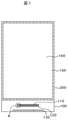
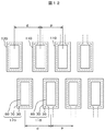
図1は本発明が適用される液晶表示装置の例である。図1は例えば、携帯電話等に使用される液晶表示装置である。図1における表示領域160において、TFTや画素電極を有する画素がマトリクス状に形成されたTFT基板100にシール材150を介してカラーフィルタ等を有する対向基板200が接着している。TFT基板100と対向電極200との間には、図示しない液晶層が挟持されている。
FIG. 1 shows an example of a liquid crystal display device to which the present invention is applied. FIG. 1 shows a liquid crystal display device used in, for example, a mobile phone. In the
TFT基板100は対向基板200よりも大きく形成されており、TFT基板100が1枚となっている部分は、ドライバIC10等を接続するIC用端子110、外部回路と接続するフレキシブル配線基板用端子130等が形成される端子領域となっている。IC用端子110の外側にはダミー端子120が形成されている。
The
IC用端子110にはIC10のバンプ20が接続される。図2は、IC10を裏面から見た斜視図である。IC10の底面には、TFT基板100のIC用端子110に対応してバンプ20が形成されている。図3は、IC10を図1に示すIC用端子110に接続した状態を示す液晶表示装置の平面図である。図13において、TFT基板100のIC用端子110にはIC10が接続しており、ICの外側にはダミー端子120が形成されている。ダミー端子120にはIC10のバンプ20は接続されていない。
The
図4は、図1におけるA部を示す平面図である。図4において、最外部のIC用端子110の外側にダミー端子120が配置している。最外部のIC用端子110の内側にはピッチpによって連続してIC用端子110が形成されている。上列のIC用端子110には表示領域160から配線が延在しており、下列のIC用端子110にはフレキシブル配線基板用端子130方向に向かって配線が延在している。一方、ダミー端子120の端子金属30は表示領域160あるいはフレキシブル配線基板用端子130側に延在する配線は存在していない。ダミー端子120は、配線接続の役割を有していないからである。
FIG. 4 is a plan view showing a portion A in FIG. In FIG. 4,
図4において、端子金属30および配線は図示しないゲート絶縁膜および無機パッシベーション膜によって保護されている。IC用端子110において、ゲート絶縁膜および無機パッシベーション膜はエッチングによってスルーホール60が形成されている。スルーホール60を覆って透明導電膜であるITO70が形成されている。ITO70は無機パッシベーション膜の端部の上にまで形成されている。ITO70は、端子金属30が水分等によって腐食されることを防止する。
In FIG. 4, the
図5は、図4のA−A断面図である。図5において、端子金属30は、TFT基板100の上に、Al合金31とキャップ金属32の積層体として形成されている。Al合金31は例えば、AlCuあるいはAlNd合金によって形成され、厚さは100nm〜300nmである。キャップメタル32は例えば、MoCrあるいはMoWによって形成され、厚さは40nm〜80nmである。
5 is a cross-sectional view taken along the line AA in FIG. In FIG. 5, the
端子金属30の上にはゲート絶縁膜40および無機パッシベーション膜50に対するスルーホール60が形成され、このスルーホール60を覆ってITO70が形成されている。図5において、最外部のIC用端子110の外側にはダミー端子120が形成されている。ダミー端子120の断面構造は、IC用端子110と同様である。最外部のIC用端子110の外側にダミー端子120が存在しているので、最外部のIC用端子110に対するエッチングにおけるローディング効果は他のIC用端子110におけるローディング効果と同じである。したがって、最外部におけるIC用端子110のスルーホール60の径もスルーホール60におけるキャップメタル32の状態も他のIC用端子110と同様にすることが出来る。
A through
図4および図5において、IC用端子110のピッチはpであるが、最外部のIC用端子110とダミー端子120とのピッチはdである。ダミー端子120は最外部のIC用端子110のローディング効果を同じにするものであるから、dとpは同じであることが理想であるが、dとpはかならずしも同じである必要は無い。dの大きさは、10μm〜100μmの範囲に設定することが出来る。10μmは、現在の製造プロセスの精度に起因する大きさであり、100μmを超えると、ローディング効果を均一にするという目的が十分に達成できないからである。
4 and 5, the pitch between the
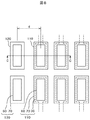
図6は、図3における領域Bの拡大平面図である。IC10の外側にダミー端子120が存在している。ダミー端子120は島状に形成された端子金属30の上にゲート絶縁膜40および無機パッシベーション膜50にスルーホール60が形成され、スルーホール60の上をITO70が覆っている構成である。
FIG. 6 is an enlarged plan view of region B in FIG. A
図7は図6のB−B断面図である。図7において、TFT基板100に形成されたIC用端子110とIC10のバンプ20とがASC90によって接続している。ASC90中の導電性粒子91によって、IC用端子110とIC10のバンプ20とが電気的導通をとっている。図7に示すように、IC10のバンプ20は、ダミー端子120とは接続していない。ダミー端子120は、最外部のIC用端子110のローディング効果を制御する役割をもつものであり、電気的な導通は必要ないからである。
7 is a cross-sectional view taken along line BB in FIG. In FIG. 7, the
ダミー端子120は、最外部のIC用端子110のローディング効果を制御するものであるから、IC用端子110と同じ形状である必要はない。すなわち、保護膜である、ゲート絶縁膜40および無機パッシベーション膜50にスルーホール60を形成するときに、最外部のIC用端子110の外側にダミー端子120のスルーホール60を同時に形成するようにすればよい。図8は、ダミー端子120に端子金属30が存在しない例である。ダミー端子120は、電気的な接続を取るものではないので、スルーホール60の下に端子金属30が存在する必要は無い。
Since the
図9は図8のC−C断面図である。図9において、ダミー端子120のスルーホール60の下には端子金属30は存在していない。ただし、IC用端子110と同様に、ダミー端子120のスルーホール60を覆ってITO70が存在している。図8および図9における最外部のIC用端子110とダミー端子120とのピッチはdであり、10μm〜100μmである。
9 is a cross-sectional view taken along the line CC of FIG. In FIG. 9, the
図10はダミー端子120をさらに単純化し、端子金属30とITO70を省略し、スルーホール60のみを形成した場合である。ローディング効果はゲート絶縁膜40および無機パッシベーション膜50にスルーホール60を形成する場合に問題となるものであるから、ゲート絶縁膜40および無機パッシベーション膜50のエッチング時にダミー端子120としてスルーホール60を形成することによってダミー端子120の役割を果たすことが出来る。
FIG. 10 shows a case where the
図11は、図10のD−D断面図である。図11において、ダミー端子120にはスルーホール60が形成されているのみである。図10および図11において、IC用端子110のピッチはpであり、最外部のIC用端子とダミー端子120のピッチはdであり、dの値は10μm〜100μmである。
11 is a cross-sectional view taken along the line DD of FIG. In FIG. 11, only the through
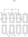
図4、8、10の例は、IC用端子110を並列に配置した例である。図4、8、10等の端子配置で説明したダミー端子120の効果は、IC用端子110が他の配列をとる場合にも同様である。図12は、IC用端子110がいわゆる千鳥配置をとる場合である。この場合もIC用端子間のピッチはpであり、最外部のIC用端子とダミー端子のピッチはdである。ダミー端子120の構成は、端子金属30に配線が接続されておらず、島状の形状である他は、IC用端子110の端子構造と同様である。図12の例もダミー端子120には、IC10のバンプ20は接続されない。
4, 8, and 10 are examples in which the
なお、ダミー端子120の端子構成は、図12の場合に限らず、図8で説明したように、端子金属30が存在しない構成、図10のように、端子金属30、ITO70のいずれも存在せず、スルーホール60のみが存在する場合でもよい。
The terminal configuration of the
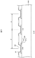
実施例1では、ダミー端子120は最外部のIC用端子110の外側に形成され、IC10を接続した場合には、IC10のバンプ20はダミー端子120には接続しない構成である。一方、IC10の標準品を使用する場合、TFT基板100に形成されたIC用端子110は、IC10のバンプ20全てと接続をする必要が無い場合もある。すなわち、IC10のバンプ20の最外部でなく、内側の複数のバンプ20と対応する箇所において、TFT基板100のIC用端子110を形成しない場合がある。このような場合、IC用端子110を形成しない部分における端部のIC用端子110はローディング効果が異なることになり、図15および図16で説明したような問題が起こりうる。図13は、この問題を対策する、TFT基板100におけるIC用端子110およびダミー端子120の配置例である。
In the first embodiment, the
図13において、両側には、複数のIC用端子110がピッチpで配列しているが、間隔qには、IC用端子110は存在しない。そうすると、IC用端子110の存在しない領域と接する端部に存在するIC用端子110のローディング効果が他のIC用端子110におけるローディング効果と異なることになる。なお、図13におけるように、IC用端子110の存在しない領域と接する端部に存在するIC用端子110も最外部のIC用端子と呼ぶ。
In FIG. 13, a plurality of
このようなローディング効果違いによる最外部のIC用端子110の信頼性の低下を防止するために、本実施例では、最外部のIC用端子110の外側にダミー端子120を形成している。このダミー端子120の構成は、図4で説明したのと同様である。ダミー端子120は、図13における左側の最外部のIC用端子110の外側にも右側の最外部のIC用端子110の外側にも形成されている。本実施例におけるダミー端子120にはIC10のバンプ20は接続される。IC用端子110のピッチはpであり、最外部のIC用端子110とダミー端子120のピッチはdである。dは10μmから100μmである。理由は実施例1で説明したのと同様である。
In order to prevent a decrease in reliability of the
また、図13におけるダミー端子120も、図8あるいは図10の端子構造でもよい。ダミー端子120の存在は、最外部のIC用端子110のローディング効果を制御するのが目的だからである。
Further, the
実施例1および実施例2におけるダミー端子120のスルーホール60の径は、図4、8、10、12、13等では、明記してないが、一般には、IC用端子110のスルーホール60の径よりも大きい。ダミー端子120は最外に位置しているので、ローディング効果の違いによってスルーホール60の径が大きくなるからである。また、ダミー端子120において、ローディング効果の違いによって、エッチングが過大になることによって、端子金属30のキャップメタル32が一部消失する場合もある。しかし、表示装置の特性には問題は無い。
The diameter of the through
以上の説明では、ゲート線を端子金属30として用いた例を説明した。しかし、本発明は、ドレイン線を端子金属30として用いた場合にも適用することが出来る。図14はドレイン線を端子金属30として用いた場合の端子の断面図である。図14において、TFT基板100の上にゲート絶縁膜40が形成され、ゲート絶縁膜40の上に端子金属80が形成されている。この場合の端子金属80は、ドレイン線と同じ構成であり、Al合金31の下にベースメタル83が形成され、Al合金の上にキャップメタル82が形成されている。Al合金81は例えば、AlCuあるいはAlNd等によって形成され、厚さは60〜200nmである。ベースメタル83は例えば、MoCrあるいはMoWによって形成され、厚さは20〜40nmである。キャップメタル82は例えば、MoCrあるいはMoWによって形成され、厚さは40〜80nm程度である。
In the above description, the example in which the gate line is used as the
このような端子金属80を覆って無機パッシベーション膜50が形成され、端子金属80の部分の無機パッシベーション膜50に対してスルーホール60が形成される。このスルーホール60を覆ってITO70が形成される。スルーホール60を形成するとき、最外部のIC用端子110がローディング効果の差によって他のIC用端子110のスルーホール60よりも大きく形成されること、あるいは、端子金属80のキャップメタル82が無機パッシベーション膜50のエッチング時に消失して、Al合金81が露出する場合があることは、ゲート線による端子金属30の場合と同様である。したがって、最外部のIC用端子110の外側にダミー端子120を形成することによって、全部のIC用端子110の信頼性を向上させることが出来る。
An
なお、図4、図8、図10、図12、図13等から明らかなように、本願発明の構成では、最外部のIC用端子110の内側にはダミー端子120は形成されていない。
As is clear from FIGS. 4, 8, 10, 12, and 13, in the configuration of the present invention, the
以上の説明は液晶表示装置に本発明を適用する場合について主に行ってきた。しかし、本発明は、液晶表示装置のみでなく、有機EL表示装置についても適用することが出来る。有機EL表示装置は、スイッチング素子としてのTFTや発光素子としての有機EL層を有する画素がマトリクス状に形成された素子基板(TFT基板)に、有機EL素子を水分等から保護するために封止基板(対向基板)が、封止材を介して接着している。そして、素子基板(TFT基板)には、ICドライバを接続するためのIC用端子が形成されている。したがって、ICドライバを接続する基本的な構成は液晶表示装置と同様であり、以上で述べた本発明は有機EL表示装置にも適用することが出来る。 The above description has been mainly performed in the case where the present invention is applied to a liquid crystal display device. However, the present invention can be applied not only to a liquid crystal display device but also to an organic EL display device. An organic EL display device is sealed on an element substrate (TFT substrate) in which pixels having a TFT as a switching element and an organic EL layer as a light emitting element are formed in a matrix to protect the organic EL element from moisture and the like. A substrate (counter substrate) is bonded via a sealing material. An IC terminal for connecting an IC driver is formed on the element substrate (TFT substrate). Therefore, the basic configuration for connecting the IC driver is the same as that of the liquid crystal display device, and the present invention described above can also be applied to an organic EL display device.
10…IC、 20…バンプ、 30…端子金属、 31…Al合金、 32…キャップメタル、 40…ゲート絶縁膜、 50…無機パッシベーション膜、 60…スルーホール、 70…ITO、 80…ドレイン線端子金属、 81…Al合金、 82…キャップメタル、 83…ベースメタル、 90…ASC、 91…導電性粒子、 100…TFT基板、 110…IC用端子、 120…ダミー端子、 130…フレキシブル配線基板用端子、 150…シール材、 160…表示領域、 200…対向基板
DESCRIPTION OF
Claims (7)
前記端子領域には、ICドライバと接続するためのIC用端子が形成され、
前記ICドライバは前記IC用端子と接続するためのバンプを有し、
前記IC用端子は所定のピッチによって複数形成され、前記複数のIC用端子の最外部に位置するIC用端子の外側には、表示領域の配線とは接続しないダミー端子が形成されており、前記最外部に位置するIC用端子の内側には、前記ダミー端子が形成されていないことを特徴とする表示装置。 A display device in which an IC driver is connected to a terminal region of a TFT substrate having a display region in which pixels including TFTs are formed in a matrix and a terminal region,
In the terminal area, an IC terminal for connection with an IC driver is formed,
The IC driver has bumps for connecting to the IC terminals,
A plurality of the IC terminals are formed with a predetermined pitch, and dummy terminals that are not connected to the wiring in the display area are formed outside the IC terminals located on the outermost side of the plurality of IC terminals, A display device characterized in that the dummy terminal is not formed inside an IC terminal located at the outermost part.
Priority Applications (3)
| Application Number | Priority Date | Filing Date | Title |
|---|---|---|---|
| JP2012088871A JP2013218126A (en) | 2012-04-10 | 2012-04-10 | Display device |
| US13/845,400 US9093592B2 (en) | 2012-04-10 | 2013-03-18 | Display device |
| US14/734,375 US9865579B2 (en) | 2012-04-10 | 2015-06-09 | Display device having driver IC directly connected to substrate |
Applications Claiming Priority (1)
| Application Number | Priority Date | Filing Date | Title |
|---|---|---|---|
| JP2012088871A JP2013218126A (en) | 2012-04-10 | 2012-04-10 | Display device |
Publications (2)
| Publication Number | Publication Date |
|---|---|
| JP2013218126A true JP2013218126A (en) | 2013-10-24 |
| JP2013218126A5 JP2013218126A5 (en) | 2015-05-28 |
Family
ID=49291602
Family Applications (1)
| Application Number | Title | Priority Date | Filing Date |
|---|---|---|---|
| JP2012088871A Pending JP2013218126A (en) | 2012-04-10 | 2012-04-10 | Display device |
Country Status (2)
| Country | Link |
|---|---|
| US (2) | US9093592B2 (en) |
| JP (1) | JP2013218126A (en) |
Families Citing this family (6)
| Publication number | Priority date | Publication date | Assignee | Title |
|---|---|---|---|---|
| JP6701777B2 (en) * | 2016-02-15 | 2020-05-27 | セイコーエプソン株式会社 | Electro-optical device, electronic equipment |
| CN109270754B (en) * | 2017-07-17 | 2021-04-27 | 京东方科技集团股份有限公司 | Array substrate and display device |
| CN109801888A (en) * | 2017-11-16 | 2019-05-24 | 群创光电股份有限公司 | First electronic component and display equipment comprising the first electronic component |
| KR102581839B1 (en) * | 2018-10-02 | 2023-09-22 | 삼성디스플레이 주식회사 | Display device |
| CN111328184B (en) * | 2020-01-20 | 2022-03-11 | 维沃移动通信有限公司 | Display screen and electronic equipment |
| DE102020135087A1 (en) | 2020-03-27 | 2021-09-30 | Samsung Electronics Co., Ltd. | Semiconductor package |
Citations (3)
| Publication number | Priority date | Publication date | Assignee | Title |
|---|---|---|---|---|
| JP2002311452A (en) * | 2001-04-13 | 2002-10-23 | Citizen Watch Co Ltd | Liquid crystal device |
| JP2006215224A (en) * | 2005-02-03 | 2006-08-17 | Sanyo Epson Imaging Devices Corp | Electrooptical device, manufacturing method of electrooptical device, and electronic device |
| JP2008165204A (en) * | 2006-12-27 | 2008-07-17 | Lg Display Co Ltd | Liquid crystal display device and fabricating method thereof |
Family Cites Families (5)
| Publication number | Priority date | Publication date | Assignee | Title |
|---|---|---|---|---|
| JP3139549B2 (en) | 1999-01-29 | 2001-03-05 | 日本電気株式会社 | Active matrix type liquid crystal display |
| JP3744450B2 (en) * | 2001-05-09 | 2006-02-08 | セイコーエプソン株式会社 | Electro-optical device, driving IC and electronic device |
| KR100698042B1 (en) * | 2002-07-29 | 2007-03-23 | 엘지.필립스 엘시디 주식회사 | Liquid Crystal Display Device And Method For Manufacturing The Same |
| US8410571B2 (en) * | 2006-07-12 | 2013-04-02 | United Microelectronics Corp. | Layout of dummy patterns |
| US7446398B2 (en) * | 2006-08-01 | 2008-11-04 | Taiwan Semiconductor Manufacturing Co., Ltd. | Bump pattern design for flip chip semiconductor package |
-
2012
- 2012-04-10 JP JP2012088871A patent/JP2013218126A/en active Pending
-
2013
- 2013-03-18 US US13/845,400 patent/US9093592B2/en active Active
-
2015
- 2015-06-09 US US14/734,375 patent/US9865579B2/en active Active
Patent Citations (3)
| Publication number | Priority date | Publication date | Assignee | Title |
|---|---|---|---|---|
| JP2002311452A (en) * | 2001-04-13 | 2002-10-23 | Citizen Watch Co Ltd | Liquid crystal device |
| JP2006215224A (en) * | 2005-02-03 | 2006-08-17 | Sanyo Epson Imaging Devices Corp | Electrooptical device, manufacturing method of electrooptical device, and electronic device |
| JP2008165204A (en) * | 2006-12-27 | 2008-07-17 | Lg Display Co Ltd | Liquid crystal display device and fabricating method thereof |
Also Published As
| Publication number | Publication date |
|---|---|
| US20150270251A1 (en) | 2015-09-24 |
| US9093592B2 (en) | 2015-07-28 |
| US9865579B2 (en) | 2018-01-09 |
| US20130264593A1 (en) | 2013-10-10 |
Similar Documents
| Publication | Publication Date | Title |
|---|---|---|
| US9568795B2 (en) | Liquid crystal display device | |
| JP5717326B2 (en) | Liquid crystal device, electronic device, and method for manufacturing liquid crystal device | |
| US20120206684A1 (en) | Liquid crystal display and manufacturing method thereof | |
| JP5192941B2 (en) | Liquid crystal display | |
| US8259247B2 (en) | Liquid crystal display device | |
| CN102053415A (en) | Horizontal-electric-field liquid crystal display apparatus | |
| US8537298B2 (en) | Liquid crystal display device | |
| US9954013B2 (en) | Display device and method of manufacturing the same | |
| US9865579B2 (en) | Display device having driver IC directly connected to substrate | |
| US10199397B2 (en) | Electrical connection structure, array substrate and display device | |
| US10288959B2 (en) | Display device comprising first and second oxide conductive films that cover a terminal wire | |
| WO2019000912A1 (en) | Display panel and manufacturing method therefor, and display apparatus | |
| JP2009031362A (en) | Wiring board, its manufacturing method, and display device | |
| US10409407B2 (en) | Touch panel and display device | |
| US9703152B2 (en) | Liquid crystal display device | |
| US9864248B2 (en) | Semiconductor device and display device | |
| JP6905421B2 (en) | Display device | |
| JP5951329B2 (en) | Liquid crystal display | |
| JP5939755B2 (en) | Liquid crystal display | |
| US20120133860A1 (en) | Active matrix substrate, liquid crystal display panel, liquid crystal display device, and method for manufacturing active matrix substrate | |
| JP5814617B2 (en) | Liquid crystal display | |
| JP5714679B2 (en) | Liquid crystal display | |
| JP2008116529A (en) | Manufacturing method of liquid crystal display panel and liquid crystal display panel |
Legal Events
| Date | Code | Title | Description |
|---|---|---|---|
| A521 | Request for written amendment filed |
Free format text: JAPANESE INTERMEDIATE CODE: A523 Effective date: 20150408 |
|
| A621 | Written request for application examination |
Free format text: JAPANESE INTERMEDIATE CODE: A621 Effective date: 20150408 |
|
| A977 | Report on retrieval |
Free format text: JAPANESE INTERMEDIATE CODE: A971007 Effective date: 20160218 |
|
| A131 | Notification of reasons for refusal |
Free format text: JAPANESE INTERMEDIATE CODE: A131 Effective date: 20160301 |
|
| A02 | Decision of refusal |
Free format text: JAPANESE INTERMEDIATE CODE: A02 Effective date: 20160906 |