JP2013201210A - Solid state imaging device - Google Patents
Solid state imaging device Download PDFInfo
- Publication number
- JP2013201210A JP2013201210A JP2012067661A JP2012067661A JP2013201210A JP 2013201210 A JP2013201210 A JP 2013201210A JP 2012067661 A JP2012067661 A JP 2012067661A JP 2012067661 A JP2012067661 A JP 2012067661A JP 2013201210 A JP2013201210 A JP 2013201210A
- Authority
- JP
- Japan
- Prior art keywords
- semiconductor layer
- photoelectric conversion
- imaging device
- state imaging
- solid
- Prior art date
- Legal status (The legal status is an assumption and is not a legal conclusion. Google has not performed a legal analysis and makes no representation as to the accuracy of the status listed.)
- Pending
Links
- 238000003384 imaging method Methods 0.000 title claims abstract description 65
- 239000007787 solid Substances 0.000 title abstract 4
- 239000004065 semiconductor Substances 0.000 claims abstract description 338
- 238000006243 chemical reaction Methods 0.000 claims abstract description 132
- 239000000463 material Substances 0.000 claims description 61
- 238000009792 diffusion process Methods 0.000 claims description 55
- 239000012535 impurity Substances 0.000 claims description 48
- 239000000969 carrier Substances 0.000 claims description 34
- 238000010521 absorption reaction Methods 0.000 claims description 11
- 230000033001 locomotion Effects 0.000 claims description 10
- 238000013459 approach Methods 0.000 claims description 7
- 229910000577 Silicon-germanium Inorganic materials 0.000 description 34
- 230000004888 barrier function Effects 0.000 description 31
- 230000014509 gene expression Effects 0.000 description 27
- 239000000758 substrate Substances 0.000 description 17
- 238000009826 distribution Methods 0.000 description 15
- 238000004088 simulation Methods 0.000 description 14
- 230000000052 comparative effect Effects 0.000 description 13
- 239000000203 mixture Substances 0.000 description 12
- 230000031700 light absorption Effects 0.000 description 11
- 230000004048 modification Effects 0.000 description 8
- 238000012986 modification Methods 0.000 description 8
- 229910021417 amorphous silicon Inorganic materials 0.000 description 7
- 238000012546 transfer Methods 0.000 description 5
- 238000010586 diagram Methods 0.000 description 4
- 238000005259 measurement Methods 0.000 description 4
- 229910021419 crystalline silicon Inorganic materials 0.000 description 3
- 230000007423 decrease Effects 0.000 description 3
- 230000007704 transition Effects 0.000 description 3
- ZOXJGFHDIHLPTG-UHFFFAOYSA-N Boron Chemical compound [B] ZOXJGFHDIHLPTG-UHFFFAOYSA-N 0.000 description 2
- 238000004458 analytical method Methods 0.000 description 2
- 229910052796 boron Inorganic materials 0.000 description 2
- 238000013461 design Methods 0.000 description 2
- 230000006866 deterioration Effects 0.000 description 2
- 230000000694 effects Effects 0.000 description 2
- 125000005842 heteroatom Chemical group 0.000 description 2
- 238000005286 illumination Methods 0.000 description 2
- 230000007246 mechanism Effects 0.000 description 2
- 230000003287 optical effect Effects 0.000 description 2
- 230000035515 penetration Effects 0.000 description 2
- OAICVXFJPJFONN-UHFFFAOYSA-N Phosphorus Chemical compound [P] OAICVXFJPJFONN-UHFFFAOYSA-N 0.000 description 1
- 239000011358 absorbing material Substances 0.000 description 1
- 230000009471 action Effects 0.000 description 1
- 230000003321 amplification Effects 0.000 description 1
- 229910052785 arsenic Inorganic materials 0.000 description 1
- RQNWIZPPADIBDY-UHFFFAOYSA-N arsenic atom Chemical compound [As] RQNWIZPPADIBDY-UHFFFAOYSA-N 0.000 description 1
- 238000005452 bending Methods 0.000 description 1
- 230000015572 biosynthetic process Effects 0.000 description 1
- 238000004364 calculation method Methods 0.000 description 1
- 230000015556 catabolic process Effects 0.000 description 1
- 230000008859 change Effects 0.000 description 1
- 238000005094 computer simulation Methods 0.000 description 1
- 230000003247 decreasing effect Effects 0.000 description 1
- 238000006731 degradation reaction Methods 0.000 description 1
- 238000000605 extraction Methods 0.000 description 1
- WPYVAWXEWQSOGY-UHFFFAOYSA-N indium antimonide Chemical compound [Sb]#[In] WPYVAWXEWQSOGY-UHFFFAOYSA-N 0.000 description 1
- 238000002347 injection Methods 0.000 description 1
- 239000007924 injection Substances 0.000 description 1
- 230000009545 invasion Effects 0.000 description 1
- 238000000034 method Methods 0.000 description 1
- 229910021421 monocrystalline silicon Inorganic materials 0.000 description 1
- 238000003199 nucleic acid amplification method Methods 0.000 description 1
- 229910052698 phosphorus Inorganic materials 0.000 description 1
- 239000011574 phosphorus Substances 0.000 description 1
- 230000008569 process Effects 0.000 description 1
- 230000006798 recombination Effects 0.000 description 1
- 238000005215 recombination Methods 0.000 description 1
- 239000000243 solution Substances 0.000 description 1
- 230000001131 transforming effect Effects 0.000 description 1
Images


Classifications
-
- H—ELECTRICITY
- H01—ELECTRIC ELEMENTS
- H01L—SEMICONDUCTOR DEVICES NOT COVERED BY CLASS H10
- H01L31/00—Semiconductor devices sensitive to infrared radiation, light, electromagnetic radiation of shorter wavelength or corpuscular radiation and specially adapted either for the conversion of the energy of such radiation into electrical energy or for the control of electrical energy by such radiation; Processes or apparatus specially adapted for the manufacture or treatment thereof or of parts thereof; Details thereof
- H01L31/08—Semiconductor devices sensitive to infrared radiation, light, electromagnetic radiation of shorter wavelength or corpuscular radiation and specially adapted either for the conversion of the energy of such radiation into electrical energy or for the control of electrical energy by such radiation; Processes or apparatus specially adapted for the manufacture or treatment thereof or of parts thereof; Details thereof in which radiation controls flow of current through the device, e.g. photoresistors
- H01L31/10—Semiconductor devices sensitive to infrared radiation, light, electromagnetic radiation of shorter wavelength or corpuscular radiation and specially adapted either for the conversion of the energy of such radiation into electrical energy or for the control of electrical energy by such radiation; Processes or apparatus specially adapted for the manufacture or treatment thereof or of parts thereof; Details thereof in which radiation controls flow of current through the device, e.g. photoresistors characterised by at least one potential-jump barrier or surface barrier, e.g. phototransistors
- H01L31/101—Devices sensitive to infrared, visible or ultraviolet radiation
- H01L31/102—Devices sensitive to infrared, visible or ultraviolet radiation characterised by only one potential barrier or surface barrier
- H01L31/105—Devices sensitive to infrared, visible or ultraviolet radiation characterised by only one potential barrier or surface barrier the potential barrier being of the PIN type
- H01L31/1055—Devices sensitive to infrared, visible or ultraviolet radiation characterised by only one potential barrier or surface barrier the potential barrier being of the PIN type the devices comprising amorphous materials of Group IV of the Periodic System
-
- H—ELECTRICITY
- H01—ELECTRIC ELEMENTS
- H01L—SEMICONDUCTOR DEVICES NOT COVERED BY CLASS H10
- H01L27/00—Devices consisting of a plurality of semiconductor or other solid-state components formed in or on a common substrate
- H01L27/14—Devices consisting of a plurality of semiconductor or other solid-state components formed in or on a common substrate including semiconductor components sensitive to infrared radiation, light, electromagnetic radiation of shorter wavelength or corpuscular radiation and specially adapted either for the conversion of the energy of such radiation into electrical energy or for the control of electrical energy by such radiation
- H01L27/144—Devices controlled by radiation
- H01L27/146—Imager structures
- H01L27/14601—Structural or functional details thereof
- H01L27/14609—Pixel-elements with integrated switching, control, storage or amplification elements
- H01L27/1461—Pixel-elements with integrated switching, control, storage or amplification elements characterised by the photosensitive area
-
- H—ELECTRICITY
- H01—ELECTRIC ELEMENTS
- H01L—SEMICONDUCTOR DEVICES NOT COVERED BY CLASS H10
- H01L27/00—Devices consisting of a plurality of semiconductor or other solid-state components formed in or on a common substrate
- H01L27/14—Devices consisting of a plurality of semiconductor or other solid-state components formed in or on a common substrate including semiconductor components sensitive to infrared radiation, light, electromagnetic radiation of shorter wavelength or corpuscular radiation and specially adapted either for the conversion of the energy of such radiation into electrical energy or for the control of electrical energy by such radiation
- H01L27/144—Devices controlled by radiation
- H01L27/146—Imager structures
- H01L27/14643—Photodiode arrays; MOS imagers
-
- H—ELECTRICITY
- H01—ELECTRIC ELEMENTS
- H01L—SEMICONDUCTOR DEVICES NOT COVERED BY CLASS H10
- H01L31/00—Semiconductor devices sensitive to infrared radiation, light, electromagnetic radiation of shorter wavelength or corpuscular radiation and specially adapted either for the conversion of the energy of such radiation into electrical energy or for the control of electrical energy by such radiation; Processes or apparatus specially adapted for the manufacture or treatment thereof or of parts thereof; Details thereof
- H01L31/08—Semiconductor devices sensitive to infrared radiation, light, electromagnetic radiation of shorter wavelength or corpuscular radiation and specially adapted either for the conversion of the energy of such radiation into electrical energy or for the control of electrical energy by such radiation; Processes or apparatus specially adapted for the manufacture or treatment thereof or of parts thereof; Details thereof in which radiation controls flow of current through the device, e.g. photoresistors
- H01L31/10—Semiconductor devices sensitive to infrared radiation, light, electromagnetic radiation of shorter wavelength or corpuscular radiation and specially adapted either for the conversion of the energy of such radiation into electrical energy or for the control of electrical energy by such radiation; Processes or apparatus specially adapted for the manufacture or treatment thereof or of parts thereof; Details thereof in which radiation controls flow of current through the device, e.g. photoresistors characterised by at least one potential-jump barrier or surface barrier, e.g. phototransistors
- H01L31/101—Devices sensitive to infrared, visible or ultraviolet radiation
- H01L31/102—Devices sensitive to infrared, visible or ultraviolet radiation characterised by only one potential barrier or surface barrier
- H01L31/109—Devices sensitive to infrared, visible or ultraviolet radiation characterised by only one potential barrier or surface barrier the potential barrier being of the PN heterojunction type
Abstract
Description
本発明の実施形態は、固体撮像装置に関する。 Embodiments described herein relate generally to a solid-state imaging device.
固体撮像装置では、複数の光電変換部のそれぞれが入射した光に応じた電荷を発生させて蓄積し、蓄積された電荷を複数の光電変換部から読み出すことにより、画像信号を得る。このとき、画像信号により得られる画像の画質を向上させるためには、各光電変換部について、光電変換効率を向上させることと、暗電流を低減させることとが望まれる。 In the solid-state imaging device, each of the plurality of photoelectric conversion units generates and accumulates charges corresponding to incident light, and reads the accumulated charges from the plurality of photoelectric conversion units to obtain an image signal. At this time, in order to improve the image quality of the image obtained from the image signal, it is desired to improve the photoelectric conversion efficiency and reduce the dark current for each photoelectric conversion unit.
1つの実施形態は、例えば、光電変換部の光電変換効率を向上でき、暗電流を低減できる固体撮像装置を提供することを目的とする。 An object of one embodiment is to provide a solid-state imaging device capable of improving the photoelectric conversion efficiency of a photoelectric conversion unit and reducing dark current, for example.
1つの実施形態によれば、光電変換部を有する固体撮像装置が提供される。光電変換部は、第1の半導体層、第2の半導体層、及び第3の半導体層を有する。第1の半導体層は、第1の導電型の半導体層である。第2の半導体層は、第1の半導体層に隣接して配されている。第2の半導体層は、第1の導電型の半導体層である。第3の半導体層は、第2の半導体層に隣接して配されている。第3の半導体層は、第2の導電型の半導体層である。第2の導電型は、第1の導電型と反対導電型である。第2の半導体層の材料の可視光に対する吸収係数は、第3の半導体層の材料の可視光に対する吸収係数より高い。固体撮像装置では、第1の半導体層の少数キャリアの拡散係数をD1m1とし、第1の半導体層の少数キャリアの拡散長をL1m1とし、第1の半導体層の真性キャリア濃度をni1とし、第1の半導体層の不純物濃度をN1とし、第2の半導体層の少数キャリアの拡散係数をD1m2とし、第2の半導体層の多数キャリアの拡散係数をD1M2とし、第2の半導体層の少数キャリアの拡散長をL1m2とし、第2の半導体層の多数キャリアの拡散長をL1M2とし、第2の半導体層の真性キャリア濃度をni2とし、第3の半導体層の少数キャリアの拡散係数をD2m3とし、第3の半導体層の少数キャリアの拡散長をL2m3とし、第3の半導体層の真性キャリア濃度をni3とし、第3の半導体層の不純物濃度をN2とするとき、D2m3/L2m3×ni3 2/N2<D1M2/L1M2×ni2 2/N2かつ、D1m1/L1m1×ni1 2/N1<D1m2/L1m2×ni2 2/N1が成り立つ。
According to one embodiment, a solid-state imaging device having a photoelectric conversion unit is provided. The photoelectric conversion unit includes a first semiconductor layer, a second semiconductor layer, and a third semiconductor layer. The first semiconductor layer is a first conductivity type semiconductor layer. The second semiconductor layer is disposed adjacent to the first semiconductor layer. The second semiconductor layer is a first conductivity type semiconductor layer. The third semiconductor layer is disposed adjacent to the second semiconductor layer. The third semiconductor layer is a second conductivity type semiconductor layer. The second conductivity type is a conductivity type opposite to the first conductivity type. The absorption coefficient for visible light of the material of the second semiconductor layer is higher than the absorption coefficient of visible light for the material of the third semiconductor layer. In the solid-state imaging device, the minority carrier diffusion coefficient of the first semiconductor layer is D 1m1 , the minority carrier diffusion length of the first semiconductor layer is L 1m1, and the intrinsic carrier concentration of the first semiconductor layer is n i1. the impurity concentration of the first semiconductor layer and N 1, the diffusion coefficient of minority carriers in the second semiconductor layer and D 1 m @ 2, a number diffusion coefficient of the carrier of the second semiconductor layer and D 1M2, the second semiconductor the diffusion length of minority carriers in the layer and L 1 m @ 2, the diffusion length of majority carriers in the second semiconductor layer and L 1M2, the intrinsic carrier concentration of the second semiconductor layer and n i2, minority carriers of the third semiconductor layer Is a diffusion coefficient of
以下に添付図面を参照して、実施形態にかかる固体撮像装置を詳細に説明する。なお、これらの実施形態により本発明が限定されるものではない。 Exemplary embodiments of a solid-state imaging device will be described below in detail with reference to the accompanying drawings. Note that the present invention is not limited to these embodiments.
(実施形態)
実施形態にかかる固体撮像装置SISについて説明する。
(Embodiment)
The solid-state imaging device SIS according to the embodiment will be described.
固体撮像装置SISは、例えばCMOSイメージセンサ又はCCDイメージセンサであり、固体撮像装置SISでは、複数の画素が1次元的に又は2次元的に配列されている。複数の画素のそれぞれは、光電変換部を有する。すなわち、固体撮像装置SISでは、複数の光電変換部のそれぞれが光電変換を行い、入射した光に応じた電荷を発生させて蓄積し、蓄積された電荷を複数の光電変換部から読み出すことにより、画像信号を得る。このとき、画像信号により得られる画像の画質を向上させるためには、各光電変換部について、光電変換効率を向上させることと、暗電流を低減させることとが望まれる。 The solid-state imaging device SIS is, for example, a CMOS image sensor or a CCD image sensor. In the solid-state imaging device SIS, a plurality of pixels are arranged one-dimensionally or two-dimensionally. Each of the plurality of pixels has a photoelectric conversion unit. That is, in the solid-state imaging device SIS, each of the plurality of photoelectric conversion units performs photoelectric conversion, generates and accumulates charges according to incident light, and reads the accumulated charges from the plurality of photoelectric conversion units. An image signal is obtained. At this time, in order to improve the image quality of the image obtained from the image signal, it is desired to improve the photoelectric conversion efficiency and reduce the dark current for each photoelectric conversion unit.
なお、固体撮像装置SISの基本構成として、例えば、2004年ごろまでは、図28(a)に示すような、CCDイメージセンサが主流であり、例えば、2004年以降2009年ごろまでは、図28(b)に示すような、半導体基板の表面側から光を入射させる表面照射型(FSI)CMOSイメージセンサが主流である。現在は、画素微細化が進んで1画素当たりの入射フォトン数が減少している実情に即して、図28(c)に示すような、配線に邪魔されず入射光を受光できるように、半導体基板の裏面側から光を入射させる裏面照射型(BSI)CMOSイメージセンサが注目されつつある。固体撮像装置の基本構成が図28(a)〜図28(c)のいずれであっても、(CMOSイメージセンサとCCDイメージセンサとで電荷を転送するための構成に違いがあるとしても、)各光電変換部の構成は同様であり、各光電変換部に要求される性能も同様であり、各光電変換部について、光電変換効率を向上させることと、暗電流を低減させることとが望まれる。以下では、固体撮像装置の基本構成が裏面照射型(BSI)CMOSイメージセンサ(図28(c)参照)である場合について例示的に説明することもあるが、本実施形態の考え方は、固体撮像装置の基本構成が他の場合であっても同様に適用できる。 As a basic configuration of the solid-state imaging device SIS, for example, until around 2004, a CCD image sensor as shown in FIG. 28A is mainstream. For example, from 2004 to around 2009, FIG. A surface irradiation type (FSI) CMOS image sensor in which light is incident from the surface side of the semiconductor substrate as shown in FIG. At present, in line with the fact that the number of incident photons per pixel is decreasing due to the progress of pixel miniaturization, as shown in FIG. A backside illumination (BSI) CMOS image sensor in which light is incident from the backside of a semiconductor substrate is drawing attention. Regardless of the basic configuration of the solid-state imaging device shown in FIGS. 28A to 28C (even if there is a difference in the configuration for transferring charges between the CMOS image sensor and the CCD image sensor). The configuration of each photoelectric conversion unit is the same, and the performance required for each photoelectric conversion unit is the same. For each photoelectric conversion unit, it is desired to improve the photoelectric conversion efficiency and reduce the dark current. . Hereinafter, a case where the basic configuration of the solid-state imaging device is a back-illuminated (BSI) CMOS image sensor (see FIG. 28C) may be described as an example, but the concept of the present embodiment is based on solid-state imaging. The present invention can be similarly applied even when the basic configuration of the apparatus is other than that.
固体撮像装置における各光電変換部として、例えば、P型の半導体層とN型の半導体層とを接合し、PN接合界面近傍で光電変換を行うように構成したフォトダイオードが挙げられる。フォトダイオードは、SiでのPN接合ダイオードが主流である。 Examples of each photoelectric conversion unit in the solid-state imaging device include a photodiode configured to join a P-type semiconductor layer and an N-type semiconductor layer and perform photoelectric conversion in the vicinity of the PN junction interface. As the photodiode, a PN junction diode of Si is mainly used.
近年では、固体撮像装置SISの高解像度化への要求を満たすために、画素の微細化が進められつつあり、それに伴い、画素を構成するフォトダイオードの間隔も狭くなる傾向にある。画素の微細化が進むとともに、斜め入射光に対する隣接画素間の混色によるノイズ劣化は深刻な問題になりつつある。例えば図24(b)に示すように、画素P801の隣接画素P802に入射した斜め入射光L801は、隣接画素P802のフォトダイオード811の半導体領域811bを通過して画素P801のフォトダイオード811の半導体領域811bまで到達するので、斜め入射光による画素P801、P802間の混色が発生しやすい。すなわち、斜め入射光に対する隣接画素間の混色を抑えることが困難である。
In recent years, in order to meet the demand for higher resolution of the solid-state imaging device SIS, pixel miniaturization is being promoted, and accordingly, the interval between photodiodes constituting the pixel tends to be narrowed. As pixels become finer, noise degradation due to color mixture between adjacent pixels with respect to obliquely incident light is becoming a serious problem. For example, as shown in FIG. 24B, the obliquely incident light L801 incident on the adjacent pixel P802 of the pixel P801 passes through the
それに対して、幾何学的な考察から、この混色を抑えるためには、フォトダイオードを薄くすればよいと考えられる。例えば図24(a)に示すように、フォトダイオード911における半導体領域911bの厚さD911をフォトダイオード811における半導体領域811bの厚さD811より薄くすると、画素P1の隣接画素P2に入射した斜め入射光L1は、隣接画素P2のフォトダイオード911の半導体領域911bを通過しても画素P1のフォトダイオード911の半導体領域911bまで到達しにくいので、斜め入射光による画素P1、P2間の混色が発生しにくい。すなわち、斜め入射光に対する隣接画素間の混色を抑えることができる。
On the other hand, it is considered from the geometrical consideration that the photodiode should be thinned in order to suppress this color mixture. For example, as shown in FIG. 24A, when the thickness D911 of the
フォトダイオードを薄く作るということは、光電変換をつかさどる半導体の体積が小さくなることを意味するから、光電変換特性の悪化につながる可能性がある。全部Siで作られたフォトダイオードでは赤色側の光吸収の進入長を考慮すると、3〜4μmほどの厚みが必要となる。すなわち、全部Siで作られたフォトダイオードを闇雲に薄くすることは、混色の問題を解決するものの、光電変換特性の悪化につながる。 Making a photodiode thin means that the volume of a semiconductor that controls photoelectric conversion is reduced, which may lead to deterioration of photoelectric conversion characteristics. A photodiode made entirely of Si requires a thickness of about 3 to 4 μm in consideration of the light absorption penetration length on the red side. That is, thinning a photodiode made entirely of Si into a dark cloud solves the problem of color mixing but leads to deterioration of photoelectric conversion characteristics.
ところが、図25(c)の表に示すように、バンドの遷移構造が同一(間接遷移か直接遷移か)の下では、バンドギャップEgが小さい材料ほど光吸収係数が高い傾向にある。これを利用すれば、光電変換特性を保った上でフォトダイオードを薄くすることが可能であると推測される。すなわち光吸収係数が高いということは、単位膜厚あたりの光電変換効率が高いことを意味するので、光電変換効率を従来と同様に維持しながらフォトダイオードを薄くすることが可能であると推測される(図25(a)、(b)参照)。例えば、図26(b)に示すように、フォトダイオードPD900において、アノード電極ANとカソード電極CAとの間でP型の半導体層902とN型の半導体層903とを接合させる際に、半導体層902の材料(例えば、Si1−xGex、0<x≦1)の光吸収係数を半導体層903の材料(例えば、Si)の光吸収係数より高くすれば、フォトダイオードPD800を全てSiで形成する場合(図26(a)に示すP型の半導体層802とN型の半導体層803とをいずれもSiで形成する場合)よりも、同等の光電変換特性が得られるようなフォトダイオードの厚みを薄くできる。
However, as shown in the table of FIG. 25C, under the same band transition structure (indirect transition or direct transition), a material having a smaller band gap Eg tends to have a higher light absorption coefficient. If this is utilized, it is presumed that the photodiode can be made thin while maintaining the photoelectric conversion characteristics. In other words, a high light absorption coefficient means that the photoelectric conversion efficiency per unit film thickness is high, and it is assumed that the photodiode can be made thin while maintaining the photoelectric conversion efficiency as in the conventional case. (See FIGS. 25A and 25B). For example, as shown in FIG. 26B, in the photodiode PD900, when the P-
しかしながら、図26(b)に示すフォトダイオードPD900は、あくまで「フォトダイオード厚を薄くして解決する混色」と「フォトダイオード厚を薄くして悪化する光電変換効率(あるいは可視光吸収効率)」とのトレードオフを適切化するための形態である。図26(b)に示すフォトダイオードPD900においては、Siよりも光吸収係数が高いSi1−xGex(0<x≦1)を導入した場合に発生し得る「暗電流の増加」に関して考慮されていない。なお、以下の説明においては、フォトダイオードの特性をモデル的に考察するためにフォトダイオードにおけるアノード側の半導体層にアノード電極ANがさらに接続され、カソード電極側の半導体層にカソード電極CAがさらに接続された形態(例えば、図26(a)、(b)に示すような形態)を扱うが、アノード電極AN及びカソード電極CAは、実装上必ずしも必要なわけではない。 However, the photodiode PD900 shown in FIG. 26 (b) is only “mixed color that can be solved by reducing the thickness of the photodiode” and “photoelectric conversion efficiency (or visible light absorption efficiency) that is deteriorated by reducing the thickness of the photodiode”. This is a form for optimizing the trade-off. In the photodiode PD900 shown in FIG. 26B, consideration is given to “increase in dark current” that can occur when Si 1-x Ge x (0 <x ≦ 1), which has a higher light absorption coefficient than Si, is introduced. It has not been. In the following description, in order to consider the characteristics of the photodiode as a model, the anode electrode AN is further connected to the anode-side semiconductor layer of the photodiode, and the cathode electrode CA is further connected to the cathode-side semiconductor layer. However, the anode electrode AN and the cathode electrode CA are not necessarily required for the mounting, although they are handled (for example, as shown in FIGS. 26A and 26B).
ここで暗電流について説明する。暗電流とは、下記の数式1に示されるように、フォトダイオードにおけるPN接合部に流れ込む少数キャリアの拡散(ドリフト)項(=右辺第一項)とPN接合部のトラップに起因する生成電流項(=右辺第二項)の和で示される、フォトダイオードのリバースバイアス側電流のことである。
Jrev=Jdiff+JGR
=q√(D/τ)×ni 2/Ndope+qniW/τg
=(少数キャリア拡散項)+(トラップ起因生成電流項)・・・数式1
Here, the dark current will be described. The dark current is a generated current term caused by a diffusion (drift) term (= first term on the right side) of minority carriers flowing into the PN junction in the photodiode and a trap at the PN junction, as shown in
J rev = J diff + J GR
= Q√ (D / τ) × n i 2 / N dope + qn i W / τ g
= (Minority carrier diffusion term) + (Trap-caused current term)
数式1において、qは電荷素量、D、τは少数キャリアの拡散係数と拡散寿命、niは真性キャリア濃度、Ndopeは少数キャリアの供給源となる領域の不純物濃度、WはPN接合の空乏層幅、τgはトラップを介して生成される生成電流の生成時間(あるいはトラップに捕獲されたキャリアの寿命)を意味する。なお、数式1では「フォトダイオードが全て同一の材料で作られていること」、かつ、「アノード電極AN側のアクセプタ濃度NA>>カソード電極CA側のドナー濃度NDの大小関係が成立していること」が想定されていることに注意したい。
In
さて、拡散の緩和時間と運動量緩和時間を同一とみなすと、拡散係数Dと拡散長L、拡散寿命τ、少数キャリアの有効質量m*の間に
D=μkBT/q=qτ/m*×kBT/q, L=√(Dτ)・・・数式2
が成立することに注意すれば、数式1の第一項の少数キャリアの拡散に関する項は、
Jdiff=q×Dp/Lp×ni 2/ND+q×Dn/Ln×ni 2/NA
=q{√(kBT/m* p)×ni 2/ND
+√(kBT/m* n)×ni 2/NA} ・・・数式3
のように整理される。ここでkBはボルツマン定数、Tは動作温度を意味する。また、下付きの添え字n,pはそれぞれ電子、ホールを意味する。
Assuming that the diffusion relaxation time and the momentum relaxation time are the same, D = μk B T / q = qτ / m * between the diffusion coefficient D, diffusion length L, diffusion lifetime τ, and effective mass m * of minority carriers . × k B T / q, L = √ (Dτ) (2)
Note that the term relating to the minority carrier diffusion in the first term of
J diff = q × D p / L p ×
= Q {√ (k B T / m * p) ×
+ √ (k B T / m * n ) × n i 2 / N A }
It is arranged like. Here, k B means Boltzmann constant, and T means operating temperature. Subscripts n and p mean electrons and holes, respectively.
また、真性キャリア濃度niは、バンドギャップEgと次の数式4に示す関係を持つことにも注意する。
ni∝exp(−Eg/(2kBT))・・・数式4
つまり、図26(b)に示すフォトダイオードPD900における例えばP型の半導体層902の材料、すなわちSiよりも光吸収効率が高い材料として、SiよりもバンドギャップEgが小さい材料(例えば、Si1−xGex、0<x≦1)を導入すると、P型の半導体層902において、キャリアの有効質量が小さくなることと、真性キャリア濃度niが増加することで、数式3に示される少数キャリアの拡散に応じた暗電流成分Jdiffが大きな値になり、すべてSiで作られたフォトダイオードPD800(図26(a)参照)よりも暗電流が増加する傾向にある。
The intrinsic carrier concentration n i is also noted to have a relationship shown in the band gap Eg and the following
n i αexp (-E g / ( 2k B T)) ··· equation (4)
That is, as a material of the P-
本発明者は、このことを確認するために、不純物濃度Ndopeがほぼ同じ状況の下で(アクセプタ濃度NAがほぼ共通の下で)、P型の半導体層902をGe分率20〜30%(すなわち、x=0.2〜0.3)程度のSi1−xGexとして図26(b)に示すようなフォトダイオードPD900を試作するとともに、その比較対象として図26(a)に示すようなフォトダイオードPD800を試作して、フォトダイオードの室温におけるI−V特性の評価を行った。その結果、図27に示すように、全てSiで形成したフォトダイオードPD800(「all Si PD実測」)に比べて、P型の半導体層902をSiよりもバンドギャップEgが小さい材料にしたフォトダイオードPD900(「SiGe/Si PD実測」)において、暗電流が3桁程度(1000倍程度)増大した。
The present inventors, in order to confirm this, the impurity concentration N dope almost under the same circumstances (under acceptor concentration N A nearly common), Ge fraction of P-
これに関して考察する。上記した「アノード電極AN側のアクセプタ濃度NA>>カソード電極CA側のドナー濃度NDの大小関係が成立していること」という想定を当てはめ、数式3のアノード電極AN側の半導体層の少数キャリアに相当する項を変形すると、
√(kBT/m* p)×ni 2/NA∝√(μn)ni 2/NA
≒√(μn)/NA×exp(−Eg/(kBT))・・・数式5
である。数式5に、Siのbulk真性電子移動度μnSiには1450cm2/Vsecを、SiGeの真性電子移動度には、Geのbulk真性電子移動度を3900cm2/VsecとしてGe分率に対して移動度の線形関係を仮定したμnSiGe=1450*0.7+3900*0.3=2185cm2/Vsecを代入する。そして、同様に線形関係を仮定して、SiのバンドギャップEgsi=1.12eVに対して、SiGeのバンドギャップEgSiGe=1.12*0.7+0.69*0.3=0.99eVを数式5に代入する。SiとSiGeの移動度比が不純物濃度Ndopeによらないという粗い見積りでは、少数キャリア拡散に関する積の数式3の比は、数式5の比に還元され、
√(μnSiGe)×exp(−EgSiGe/(kBT))/√(μnSi)×exp(−Egsi/(kBT))=180=(2桁)・・・数式6
となるので、数式見積り上は、暗電流比は二桁程度増大してしまうと予想される。一方、図27を見ると、SiGeを導入することで3桁程度(1000倍程度)増大してしまうことが認められる。すなわち、SiGeを導入することで、実験的にも理論的にも暗電流は増大することが確認された。
Consider this. Applying the above-mentioned assumption that “the acceptor concentration N A >> on the anode electrode AN side >> the donor concentration N D on the cathode electrode CA side is satisfied”, the number of semiconductor layers on the anode electrode AN side in
√ (k B T / m * p) ×
≒ √ (μ n) / N A × exp (-E g / (k B T)) ···
It is. In
√ (μ nSiGe ) × exp (−Eg SiGe / (k B T)) / √ (μ nSi ) × exp (−Eg si / (k B T)) = 180 = (2 digits)
Therefore, it is expected that the dark current ratio will increase by about two orders of magnitude in estimating the mathematical formula. On the other hand, it can be seen from FIG. 27 that the introduction of SiGe increases it by about 3 digits (about 1000 times). That is, it was confirmed that the dark current increases experimentally and theoretically by introducing SiGe.
増大比が数式5及び数式6の理論と定量的に異なる理由は、Si基板との格子不整合等の理由でトラップサイトがヘテロ界面に存在し、数式1中のトラップ起因の生成電流項が増えていることなどが想定しうる。
The reason why the increase ratio is quantitatively different from the theory of
さて、上記ではSiよりも光吸収効率が高い材料として、SiよりもバンドギャップEgが小さいSi1−xGex(0<x≦1)の導入を例に説明している。しかしながら、図25(a)〜(c)に示されるように、例えばInxGa1−xAsやInPなど、SiよりもバンドギャップEgが大きい高光吸収材料もありうる。その場合でも肝要なのは、単にバンドギャップEgの大小の議論ではなく、数式3に規定された電流輸送に関連した、少数キャリアの不純物濃度Ndope、拡散係数D、拡散長L、及び真性キャリア濃度niによる関係式
D/L×ni 2/Ndope・・・数式7
の大小関係である。数式7の関係式が、例えば全てSiで作成した場合よりも大きいと、やはり全てSiで作成したよりも暗電流が増加してしまうことに注意したい。
In the above description, the introduction of Si 1-x Ge x (0 <x ≦ 1), which has a band gap Eg smaller than that of Si, is described as an example as a material having higher light absorption efficiency than Si. However, as shown in FIGS. 25A to 25C, there may be a highly light-absorbing material having a band gap Eg larger than that of Si, such as In x Ga 1-x As and InP. Even in that case, what is important is not simply a discussion of the magnitude of the band gap Eg, but the minority carrier impurity concentration N dope , the diffusion coefficient D, the diffusion length L, and the intrinsic carrier concentration n related to the current transport defined in
It is a big and small relationship. It should be noted that if the relational expression of
このような暗電流の増加は、光信号がない暗時であるにもかかわらず光信号が入った「ON」であると解釈されて信号増幅がされる、いわゆる「暗時ノイズ」の増加につながる。すなわち、「混色」と「光電変換効率」のトレードオフは、図26(b)に示すようなSi1−xGex(0<x≦1)の導入で解決できるものの、それらと「暗電流」トレードオフの解決に関しては、図26(b)に示す形態では必ずしも解決できない傾向にある。 Such an increase in dark current results in an increase in so-called “dark noise” that is interpreted as being “ON” with an optical signal in spite of the dark time when there is no optical signal and the signal is amplified. Connected. That is, the tradeoff between “color mixture” and “photoelectric conversion efficiency” can be solved by introducing Si 1-x Ge x (0 <x ≦ 1) as shown in FIG. Regarding the solution of the trade-off, the form shown in FIG.
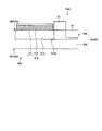
そこで、本実施形態では、図1に示すように、半導体層3とより光吸収係数の高い半導体層2とでPN接合を形成した構成(例えば、図26(b)参照)をベースとして、数式7の関係式が半導体層2より小さい半導体層1をさらに追加することで、暗電流の低減を図る。
Therefore, in the present embodiment, as shown in FIG. 1, a mathematical formula is formed based on a configuration in which a PN junction is formed by the
具体的には、本実施形態にかかる固体撮像装置SISは、複数の画素Pを備える。各画素Pは、光電変換部PDを有する。光電変換部PDは、例えばPN接合界面を有し、受けた光をPN接合界面近傍で光電変換し、光に応じた電荷を発生させて蓄積する。 Specifically, the solid-state imaging device SIS according to the present embodiment includes a plurality of pixels P. Each pixel P has a photoelectric conversion unit PD. The photoelectric conversion unit PD has, for example, a PN junction interface, photoelectrically converts received light in the vicinity of the PN junction interface, and generates and accumulates charges corresponding to the light.
各画素Pの光電変換部PDは、図1に示すように、第1の半導体層1、第2の半導体層2、及び第3の半導体層3を有する。なお、図1には半導体基板を示していないが、光電変換部PDでは、例えば、第1の半導体層1側が半導体基板の表面側であり、第3の半導体層3側が半導体基板の裏面側である。
As illustrated in FIG. 1, the photoelectric conversion unit PD of each pixel P includes a
第1の半導体層1は、第2の半導体層2に隣接して配されている。第1の半導体層1は、例えば、第2の半導体層2の主面2aに配されている。第1の半導体層1は、例えば、第1の導電型(例えば、P型)の不純物を含む半導体(例えば、Si)で形成されている。P型の不純物は、例えば、ボロンである。第1の半導体層1の材料(例えば、Si)のバンドギャップは、例えば、第3の半導体層3の材料(例えば、Si)のバンドギャップと均等である。
The
第2の半導体層2は、第1の半導体層1に隣接して配されている。第2の半導体層2は、例えば、主面2a及び主面2bを有する。主面2bは、主面2aの反対側の主面である。第2の半導体層2は、例えば、第1の導電型(例えば、P型)の不純物を含む半導体(例えば、Si1−xGex、0<x≦1)で形成されている。P型の不純物は、例えば、ボロンである。また、第2の半導体層2の材料(例えば、Si1−xGex、0<x≦1)の可視光に対する吸収係数は、第3の半導体層3の材料(例えば、Si)の可視光に対する吸収係数より高い(図25(a)〜(c)参照)。第2の半導体層2の材料(例えば、Si1−xGex、0<x≦1)のバンドギャップは、例えば、第1の半導体層1の材料(例えば、Si)のバンドギャップより小さく、かつ、第3の半導体層3の材料(例えば、Si)のバンドギャップより小さい。
The
なお、第2の半導体層2の材料の可視光に対する吸収係数が第3の半導体層3の材料の可視光に対する吸収係数より高ければ、第2の半導体層2の材料は、そのバンドギャップが第3の半導体層3の材料(例えば、Si)のバンドギャップより大きいもの(例えば、InxGa1−xAsやInPなど)であってもよい(図25(a)〜(c)参照)。
If the absorption coefficient of visible light of the material of the
第3の半導体層3は、第2の半導体層2に隣接して配されている。例えば、第3の半導体層3は、第1の半導体層1と反対側で第2の半導体層2に隣接して配されている。例えば、第3の半導体層3は、第2の半導体層2の主面2bに配されている。第3の半導体層3は、例えば、第2の導電型(例えば、N型)の不純物を含む半導体(例えば、Si)で形成されている。N型の不純物は、例えば、リン又は砒素である。第3の半導体層3の材料(例えば、Si)のバンドギャップは、例えば、第1の半導体層1の材料(例えば、Si)のバンドギャップと均等である。
The
第2の導電型は、第1の導電型と反対導電型である。すなわち、光電変換部PDでは、第2の半導体層2と第3の半導体層3との界面がPN接合界面として機能する。
この固体撮像装置SISでは、
D2m3/L2m3×ni3 2/N2<D1M2/L1M2×ni2 2/N2・・・数式8
かつ、
D1m1/L1m1×ni1 2/N1<D1m2/L1m2×ni2 2/N1・・・数式9
が成り立つ。
The second conductivity type is a conductivity type opposite to the first conductivity type. That is, in the photoelectric conversion unit PD, the interface between the
In this solid-state imaging device SIS,
D 2m3 / L 2m3 × n i3 2 / N 2 <D 1M2 / L 1M2 × n i2 2 / N 2.
And,
D 1m1 / L 1m1 × n i1 2 / N 1 <D 1m2 / L 1m2 × n i2 2 / N 1 Equation 9
Holds.
数式8、9において、第1の半導体層1の少数キャリアの拡散係数をD1m1とし、第1の半導体層1の少数キャリアの拡散長をL1m1とし、第1の半導体層1の真性キャリア濃度をni1とし、第1の半導体層1の不純物濃度をN1としている。また、第2の半導体層2の少数キャリアの拡散係数をD1m2とし、第2の半導体層2の多数キャリアの拡散係数をD1M2とし、第2の半導体層2の少数キャリアの拡散長をL1m2とし、第2の半導体層2の多数キャリアの拡散長をL1M2とし、第2の半導体層2の真性キャリア濃度をni2としている。また、第3の半導体層3の少数キャリアの拡散係数をD2m3とし、第3の半導体層3の少数キャリアの拡散長をL2m3とし、第3の半導体層3の真性キャリア濃度をni3とし、第3の半導体層3の不純物濃度をN2としている。なお、添え字として、第1の導電型の少数キャリアを「1m」で表し、第1の導電型の多数キャリアを「1M」で表し、第2の導電型の少数キャリアを「2m」で表している。
In
あるいは、第1の半導体層1の少数キャリアの移動度をμ1m1とし、第2の半導体層2の少数キャリアの移動度をμ1m2とし、第2の半導体層2の多数キャリアの移動度をμ1M2とし、第3の半導体層3の少数キャリアの移動度をμ2m3とすると、数式2,3で述べた関係から、これらを用いて数式8、9を書き直すことができて、数式10、11のようになる。すなわち、固体撮像装置SISでは、
√(μ2m3)×ni3 2/N2<√(μ1M2)×ni2 2/N2・・・数式10
かつ、
√(μ1m1)×ni1 2/N1<√(μ1m2)×ni2 2/N1・・・数式11
が成り立つ。
Alternatively, the mobility of minority carriers in the
√ (μ 2m3 ) × n i3 2 / N 2 <√ (μ 1M2 ) × n i2 2 / N 2 Formula 10
And,
√ (μ 1m1 ) × n i1 2 / N 1 <√ (μ 1m2 ) × n i2 2 / N 1 Formula 11
Holds.
言い換えると、固体撮像装置SISでは、各光電変換部PDにおいて、第2の半導体層2の材料・構造を、第1の半導体層1の材料・構造や第3の半導体層3の材料・構造との関係で、数式8かつ数式9を満たすように、あるいは、数式10かつ数式11を満たすように、構成する。これにより、例えば、第1の半導体層1を、第2の半導体層2に対して暗電流を抑制するためのバリア(少数キャリア拡散流入を防ぐ障壁)として機能させることができる。なお、以下では、第1の半導体層1を第2の半導体層2に対するバリア(少数キャリア拡散流入を防ぐ障壁)として機能する層という意味でバリア層と呼ぶことがある。
In other words, in the solid-state imaging device SIS, in each photoelectric conversion unit PD, the material / structure of the
より具体的には、固体撮像装置SISは、例えば裏面照射型(BSI)CMOSイメージセンサ(図28(c)参照)であり、例えば第3の半導体層3側が光入射側であり、例えば光入射側にある第3の半導体層3がN型の半導体層であり、第2の半導体層2及び第1の半導体層1がそれぞれP型の半導体層である。すなわち、第1の導電型がP型であり第2の導電型がN型である。この場合、第1の導電型の少数キャリア「1m」が電子になるので、「1m」を電子を表す「n」で置き換え、第1の導電型の多数キャリア「1M」がホールになるので、「1M」をホールを表す「p」で置き換え、第2の導電型の少数キャリア「2m」がホールになるので、「2m」をホールを表す「p」で置き換え、第1の導電型の不純物濃度N1がアクセプタ濃度になるので、「N1」をアクセプタ濃度を表す「NA」で置き換え、第2の導電型の不純物濃度N2がドナー濃度になるので、「Ns」をドナー濃度を表す「ND」で置き換えると、数式8、9は、下記の数式12、13のようになる。すなわち、固体撮像装置SISでは、
Dp3/Lp3×ni3 2/ND<Dp2/Lp2×ni2 2/ND・・・数式12
かつ、
Dn1/Ln1×ni1 2/NA<Dn2/Ln2×ni2 2/NA・・・数式13
が成り立つ。
More specifically, the solid-state imaging device SIS is, for example, a back-illuminated (BSI) CMOS image sensor (see FIG. 28C), for example, the
D p3 / L p3 × n i3 2 / N D <D p2 / L p2 × n i2 2 / N D Equation 12
And,
D n1 / L n1 × n i1 2 / N A <D n2 / L n2 × n
Holds.
あるいは、上記のように置き換えると、数式10、11は、下記の数式12、13のようになる。固体撮像装置SISでは、
√(μp3)×ni3 2/ND<√(μp2)×ni2 2/ND・・・数式14
かつ、
√(μn1)×ni1 2/NA<√(μn2)×ni2 2/NA・・・数式15
が成り立つ。
Or if it replaces as mentioned above,
√ (μ p3) × n i3 2 / N D <√ (μ p2) ×
And,
√ (μ n1) × n i1 2 / N A <√ (μ n2) × n
Holds.
言い換えると、固体撮像装置SISでは、各光電変換部PDにおいて、第2の半導体層2の材料・構造を、第1の半導体層1の材料・構造や第3の半導体層3の材料・構造との関係で、数式12かつ数式13を満たすように、あるいは、数式14かつ数式15を満たすように、構成する。
In other words, in the solid-state imaging device SIS, in each photoelectric conversion unit PD, the material / structure of the
なお、以下の説明においては、光電変換部PD(例えば、フォトダイオード)の特性をモデル的に考察するために光電変換部PDにおけるアノード側の半導体層にアノード電極ANがさらに接続され、カソード電極側の半導体層にカソード電極CAがさらに接続された形態(例えば、図1に示すような形態)を扱うが、アノード電極AN及びカソード電極CAは、実装上必ずしも必要なわけではない。 In the following description, an anode electrode AN is further connected to the anode-side semiconductor layer in the photoelectric conversion unit PD in order to consider the characteristics of the photoelectric conversion unit PD (for example, a photodiode) as a model, and the cathode electrode side In this embodiment, the cathode electrode CA is further connected to the semiconductor layer (for example, as shown in FIG. 1), but the anode electrode AN and the cathode electrode CA are not necessarily required for mounting.
本発明者は、実施形態における光電変換部PDの構成による効果を検証するために、コンピュータシミュレーションを行ったので、以下にそのシミュレーション結果について説明する。
まず、ダングリングボンド等によるキャリアのトラップがない場合(=数式1の少数キャリア拡散項のみに着目する場合)についてシミュレーションを行った。
Since this inventor performed computer simulation in order to verify the effect by the structure of the photoelectric conversion part PD in embodiment, the simulation result is demonstrated below.
First, a simulation was performed in the case where there was no trapping of carriers due to dangling bonds or the like (= when focusing only on the minority carrier diffusion term of Formula 1).
具体的には、光電変換部PD(例えば、フォトダイオード)の構造として図2(a)〜(e)に示す5種類の構造A〜Eをシミュレーション上用意して、各々の、T=333Kにおける光電変換部PD(例えば、フォトダイオード)のI−V特性を計算し、暗電流を評価した。 Specifically, five types of structures A to E shown in FIGS. 2A to 2E are prepared for simulation as the structure of the photoelectric conversion unit PD (for example, a photodiode), and each of the structures at T = 333K is prepared. The IV characteristic of photoelectric conversion part PD (for example, photodiode) was calculated, and dark current was evaluated.
5種類の構造A〜Eのうち、構造C〜構造Eが本実施形態に対応したものであり、構造A及び構造Bは比較例である。 Of the five types of structures A to E, structures C to E correspond to the present embodiment, and structures A and B are comparative examples.
図2(a)に示す構造Aは、図26(b)に示すフォトダイオードPD900に対応したものであり、SiGe層902aに直接アノード電極ANをつけたものである。ただし、SiGe層902aの組成は、SiGe層902aの表面近傍の部分をGe組成率30%、SiGe層902aとSi層903aとの界面近傍の部分をGe組成率20%とし、その間は線形に変化するものとしている。SiGe層902aの厚さを400nmとし、Si層903aの厚さを1.5μmとした。
Structure A shown in FIG. 2A corresponds to the photodiode PD900 shown in FIG. 26B, and is obtained by directly attaching the anode electrode AN to the
図2(b)に示す構造Bは、図26(a)に示すフォトダイオードPD800に対応したものであり、全てSiで作成したもの(今は暗電流のみに着目したシミュレーションであるため、Siの厚みは3μm以上確保せずに2μmとしたもの)である。構造Bは、厚さ2μmのSi層において、アノード電極側ANにP型Si層802bを有し、カソード電極CA側にN型Si層803bを有するものとした。
The structure B shown in FIG. 2B corresponds to the photodiode PD800 shown in FIG. 26A, and is made entirely of Si (since it is a simulation focusing only on dark current, The thickness is 2 μm without securing 3 μm or more). In the structure B, a Si layer having a thickness of 2 μm has a P-
図2(c)に示す構造Cは、構造Aに対してアノード電極ANとSiGe層902a(SiGe層2c)との間にバリア層1cを追加したものに相当する構成である。バリア層1cとして、bulk Siの移動度と同等な単結晶Si(c−Si)を用いることを仮定したものである。バリア層1cの厚さを100〜300nmとし、SiGe層902aの厚さを400nmとし、Si層903aの厚さを1.5μmとした。以下において、構造Cのことを、実施例2の構造と呼ぶこともある。
The structure C shown in FIG. 2C corresponds to a structure in which a
図2(d)に示す構造Dは、構造Aに対してアノード電極ANとSiGe層902a(SiGe層2d)との間にバリア層1dを追加したものに相当する構成である。バリア層1dとして、bulk Siよりも移動度が1/100小さいアモルファスSi(a−Si)を用いることを仮定したものである。バリア層1dの厚さを100〜300nmとし、SiGe層902aの厚さを400nmとし、Si層3dの厚さを1.5μmとした。以下において、構造Dのことを、実施例1の構造と呼ぶこともある。
The structure D shown in FIG. 2D corresponds to a structure in which a barrier layer 1d is added between the anode A and the
図2(e)に示す構造Eは、構造Aに対してアノード電極ANとSiGe層902a(SiGe層2e)との間にバリア層1eを追加したものに相当する構成である。単にバンドギャップEgの大小ではなく、数式7の関係式の大小関係が重要であることを明示するために、バリア層1eとして、bulk Siと移動度が仮想的に同等であるアモルファスSi(a−Si)を用いることを仮定したものである。
The structure E shown in FIG. 2E is a structure corresponding to the structure A in which a barrier layer 1e is added between the anode electrode AN and the
数式1に示されるように、不純物濃度Ndopeも暗電流の制御パラメータであるので、これらの構造A〜構造Eに対しては、図3に示すようにバリア層の厚みやドナーやアクセプタと言った不純物分布も振ってシミュレーションを行った。
As shown in
加えて、検討に用いたシミュレータは、図4のように実測と定量的にも良好に一致することを確かめた、いわゆるキャリブレーション済みのシミュレータであることを強調する。 In addition, it is emphasized that the simulator used for the examination is a so-called calibrated simulator that has been confirmed to be in good agreement with the actual measurement as shown in FIG.
図5は、図2に示す構造A〜構造Eと図3に示す不純物分布との条件を組み合わせて、I−V特性をシミュレーションした結果である。ここで、図5に示された種類の異なる線(実線や破線)は、上述のような図2の構造と図3の不純物分布を組み合わせて振った各条件の線に相当する(後述の図7−1、図7−2や図8の線も同義である)。なお、この検討においてはまだトラップ起因の生成電流に由来する暗電流はシミュレーションで考慮していない。トラップを考慮した検討は後述する。 FIG. 5 is a result of simulating IV characteristics by combining the conditions of the structures A to E shown in FIG. 2 and the impurity distribution shown in FIG. Here, different types of lines (solid lines and broken lines) shown in FIG. 5 correspond to the lines of the respective conditions that are shaken by combining the structure of FIG. 2 and the impurity distribution of FIG. 3 (described later). 7-1, FIG. 7-2, and the line of FIG. 8 are also synonymous. In this study, the dark current derived from the generated current due to the trap is not yet considered in the simulation. The examination considering the trap will be described later.
図5から、光電変換部PDのリバース側電流である暗電流を、アノード電極ANの電圧Va=−1.0Vのときのアノード電流であると定義し、まとめたのが図6である。図6の横軸は、図3で示したドナー分布条件が対応する。図6を見ると、構造A(構造AA〜構造AC)の暗電流がバリア厚み(A,B,C)やドナー不純物分布条件(1−27)によらず、他の構造B〜構造Eに比して2−3桁程度暗電流が多いことが分かる。一方で、構造C(構造CA〜構造CC=実施例2)、構造D(構造DA〜構造DC=実施例1)は、全てSiで作った場合の構造B(構造BA〜構造BC)と同等まで、暗電流を抑制できることが分かる。 From FIG. 5, the dark current that is the reverse-side current of the photoelectric conversion unit PD is defined as the anode current when the voltage Va of the anode electrode AN = −1.0 V and is summarized in FIG. 6. The horizontal axis in FIG. 6 corresponds to the donor distribution condition shown in FIG. Referring to FIG. 6, the dark current of structure A (structure AA to structure AC) changes to other structures B to E regardless of the barrier thickness (A, B, C) or donor impurity distribution condition (1-27). It can be seen that the dark current is much larger by about 2-3 digits. On the other hand, the structure C (structure CA to structure CC = example 2) and the structure D (structure DA to structure DC = example 1) are all equivalent to the structure B (structure BA to structure BC) when made of Si. It can be seen that the dark current can be suppressed.
特筆すべきは構造Dと構造Eの比較であり、この2つの構造は、図2(d)、(e)及び図7−1(d)、(e)に示すように、バリア層のバンドギャップEgや不純物分布状況は同様であるが、バリア層の少数キャリアである電子移動度が異なる。図6によれば、構造Eの暗電流値は構造Dの暗電流と比べると、一桁程度増えていることがわかる。単にバリア層のバンドギャップEgと、Siよりも可視光吸収係数が大きい層のバンドギャップEgとの間の、バンドギャップEgの大小のみが問題であるというのならば、構造Dの暗電流と構造Eの暗電流との分析結果は同じになるはずである。すなわち、得られた構造Dの暗電流と構造Eの暗電流との分析結果は、単にバンドギャップEgの大小ではなく、数式7の関係式(すなわち、少数キャリアの項D/Lとni 2/Ndopeとの積)の大小関係が、少数キャリア拡散による暗電流を決めていることを、如実に強調していると言える。 It should be noted that the structure D and the structure E are compared, and the two structures are shown in FIGS. 2D and 2E and FIGS. 7-1D and 7E. Although the gap Eg and the impurity distribution are the same, the electron mobility which is a minority carrier of the barrier layer is different. According to FIG. 6, it can be seen that the dark current value of the structure E is increased by an order of magnitude compared with the dark current of the structure D. If only the magnitude of the band gap Eg between the band gap Eg of the barrier layer and the band gap Eg of the layer having a larger visible light absorption coefficient than Si is a problem, the dark current and the structure of the structure D The analysis result of E with dark current should be the same. That is, the analysis result of the dark current of structure D and the dark current of structure E obtained is not simply the magnitude of the band gap Eg, but the relational expression of Equation 7 (that is, the minority carrier terms D / L and n i 2 It can be said that the magnitude relationship of (product with / N dope ) emphasizes the fact that the dark current due to minority carrier diffusion is determined.
さて、上記の実施例1、2が数式12、13そしてそれを変形した数式14、15の関係を満たしているか確かめてみる。まずは、図7−1(a)〜(e)に電子移動度μnの分布、図7−2(a)〜(e)にホール移動度μpの分布、そして図8(a)〜(e)に√(pn)の分布図をそれぞれ示した上で、それらと図3の不純物分布条件から計算できる、電極近傍の「少数キャリアの項D/L(∝√(μ))とni 2/Ndopeとの積」の大小を表にして比較したものが図9である。ここで、各μは数式5の下で議論した真性移動度値ではなく、シミュレーションの中で不純物濃度の関数になった移動度になっていることに注意する。真性キャリア濃度ni値の抽出には、熱平衡が保たれている電極近傍の半導体領域においてはpn=ni 2というpn積が成立しているはずであるので、図8における各構造のz=0の地点(=アノード電極とPDの接点)やzの負側の終端部の地点(=カソード電極とPDの接点)の縦軸値が真性キャリア濃度niに相当することを利用した。SiGe層をそのままアノード電極につけた構造Aの積(数式7参照)の値を、図9(a)では太枠で囲って強調した。それらと比べて、実施例2、1すなわち構造C、Dともに積(数式7参照)の値が小さいことがわかる。したがって、まず実施例1,2が数式13、そしてそれを変形した15の関係を満たしていることが確かめられた。一方で、図9(b)の最終行にはSiGe層をそのままカソード電極につけた場合の積の関係を計算し、太枠で囲って強調した。この数字と比べて、図9(b)の実施例2,1すなわち構造C,Dの積の値はいずれも小さいことがわかる。したがって、実施例1、2は数式12、そしてそれを変形した数式14の関係を満たしていることも同時に確かめられた。以上のことから、実施例1、2は数式12、13そしてそれを変形した数式14、15の関係を両方とも満たしていることが確かめられた。このように、図6のような暗電流の大小関係が得られた理由は、「数式12−15のような大小関係を満たしていたからそうなった」と結論付けることができる。
Now, let's check whether the above-mentioned Examples 1 and 2 satisfy the relations of
次に、ダングリングボンド等によるキャリアのトラップがある場合(=数式1のトラップ項もかかわる場合)についてシミュレーションを行った。
Next, a simulation was performed in the case where there was a carrier trap due to dangling bonds or the like (= the case where the trap term of
上記では暗電流にトラップ起因項がない場合、すなわち少数キャリア拡散のみが暗電流を支配している場合についてシミュレーションを行った結果について述べた。しかしながら、数式5、6を用いて実測におけるSiGe/Siとall Siの暗電流差を考察した場合のように、少数キャリア拡散のみで暗電流が定量的に説明できる場合は稀である。
さて、数式1に記したトラップ起因の電流に関する生成項のうちni/τgの部分(次元1/cm3sec)は、Shockley−Read−Hall(SRH model)によれば、
ni/τg=GRSRH
=(pn−nie 2)/{τgn(p+nieexp(Etrap/kBT))
+τgp(n+nieexp(−Etrap/kBT))}・・・数式16
のように書き下すことができることが知られている。ここで、p、nは、ホール、電子の濃度、τgはトラップに捕獲されたキャリアの寿命で、添え字n、pはそれぞれ電子、ホールのものを意味する。Etrapはトラップの禁制帯内のエネルギー準位で、nieは平衡状態の真性キャリア濃度である。τgは、トラップの濃度Ntrapに反比例することが知られる(1/τg∝Ntrap)。
In the above description, the simulation results are described in the case where there is no trap-induced term in the dark current, that is, only the minority carrier diffusion dominates the dark current. However, it is rare that the dark current can be quantitatively explained only by minority carrier diffusion, as in the case where the dark current difference between SiGe / Si and all Si in the actual measurement is considered using
Now, n i / τ g portion of the product section on trap-induced currents noted in Equation 1 (dimension 1 / cm 3 sec), according to Shockley-Read-Hall (SRH model ),
n i / τ g = GR SRH
= (Pn−n ie 2 ) / {τ gn (p + n ie exp (E trap / k B T))
+ Τ gp (n + n ie exp (−E trap / k B T))}
It is known that it can be written down as Here, p and n are the concentrations of holes and electrons, τ g is the lifetime of the carriers trapped in the trap, and the subscripts n and p are those of electrons and holes, respectively. E trap is the energy level within the forbidden band of the trap, and nie is the intrinsic carrier concentration in the equilibrium state. It is known that τ g is inversely proportional to the trap concentration N trap (1 / τ g ∝N trap ).
さて、数式16の意味するところは、たとえトラップがあったとしても、平衡状態であれば(=バンドが曲がっていない状態であれば)、トラップ起因のGR項はゼロになるということである。このことは、平衡状態ではpn積とnieの間に、
pn=nie 2・・・数式17
という質量作用則(pn積一定)が成立し、数式16の分子が0になることから容易に理解される。逆に言うと、このpn積一定から著しくずれるところ(=バンドが曲がっているところ)にトラップが大量にあると(トラップ寿命が短いと)、トラップ起因の生成電流が増えるということを意味する。そして、バンドが曲がっている所とは、PD動作時に、バイアスと空間電荷の関数によって空乏層が広がっている領域に他ならない。
The meaning of
pn = n ie 2 Equation 17
This is easily understood from the fact that the mass action law (constant pn product) is established and the numerator of
トラップがある場合は、もっとも平衡からずれている領域(空乏層幅の両端から中央側に離れた領域)とトラップの位置が重なると、トラップ起因暗電流項が増大してしまうと考えられる。ゆえに発明の効果を見極めるに当たっては、トラップと不純物分布の関係についても留意すべきなのは明白である。そこで、シミュレーションにおいては、図2の構造と図3の不純物条件は固定したままで、格子定数の差によりトラップが生成されやすいと考えられる、SiGe/Siへテロ界面近傍にトラップサイトが分布していると仮定し、そのトラップサイトが数式16のようなSRHモデルを起因とする生成電流を生じると仮定する。そのような仮定の下で、シミュレーションを行った。端的に言うと、もっともらしいトラップを考慮したシミュレーションを行った。
In the case where there is a trap, it is considered that the trap-induced dark current term increases if the region most deviated from equilibrium (the region far from the both ends of the depletion layer width to the center side) and the position of the trap overlap. Therefore, it is clear that the relationship between the trap and the impurity distribution should be noted when determining the effect of the invention. Therefore, in the simulation, trap sites are distributed in the vicinity of the SiGe / Si heterointerface, which is considered to generate traps easily due to the difference in lattice constant, while the structure of FIG. 2 and the impurity condition of FIG. 3 remain fixed. It is assumed that the trap site generates a generated current due to the SRH model as shown in
トラップがない場合の図5のようにI−V特性を計算した後、アノード電極ANの電圧Va=−1V地点の電流を暗電流とし、トラップがない場合の図6のように横軸をドナー不純物条件とし、縦軸を暗電流としてまとめたものが、図10(b)〜(d)である。すなわち、Ntrapの関数である寿命についてτgn=τgp=τgと仮定し、1e−6sec、1e−8sec、1e−10secの3種類の条件でシミュレーションした結果が図10(b)〜(d)である。また、比較のために、トラップがない場合(すなわち、図6と同じもの)も図10(a)として示している。構造Bのみに関しては、あくまでレファレンスとしての役目(レファレンスSi)を担わせるため、図10(a)〜(d)の4つのグラフのいずれもがトラップがないとした計算結果を用いている。ちなみに、図4の「SiGe/Si PD」の実測/シミュレーション比較は、τgに1.0e−8secを代入して得られたものである。このことから、図10で調査した3種類の寿命の中では、τg=1.0e−8secとして計算した結果が、一番もっともらしいと考えられる。 After calculating the IV characteristic as shown in FIG. 5 when there is no trap, the current at the point of voltage Va = −1V of the anode electrode AN is set as a dark current, and the horizontal axis is the donor as shown in FIG. 6 when there is no trap. FIGS. 10B to 10D show the impurity conditions and the vertical axis as dark current. That is, assuming that the lifetime as a function of N trap is τ gn = τ gp = τ g , the simulation results under three conditions of 1e-6 sec, 1e-8 sec, 1e-10 sec are shown in FIGS. d). For comparison, the case where there is no trap (that is, the same as that shown in FIG. 6) is also shown in FIG. For the structure B only, the calculation result assuming that there is no trap in any of the four graphs of FIGS. 10A to 10D is used in order to play a role as a reference (reference Si). Incidentally, the measured / simulated comparison of "SiGe / Si PD" in FIG. 4, is obtained by substituting 1.0e-8 sec to tau g. From this, among the three types of lifetimes investigated in FIG. 10, the result calculated with τ g = 1.0e-8 sec is considered the most plausible.
そして、図10を別の見方で表したものが図11である。横軸のτtrapとは上で述べたτgのことであり、縦軸が暗電流値である。前述したように、τgはトラップ濃度Ntrapに反比例するため、図11の横軸の値はそれが大きいほどトラップ濃度が小さくて、トラップフリーなきれいな光電変換部PDであることを意味する。図11からは、構造C(=実施例2)や構造D(=実施例1)の場合であれば、曲線によっては、すなわち不純物分布条件によっては、調査したトラップ濃度範囲(x軸範囲)によらず、構造B(レファレンスSi)のレベルと同等の暗電流が実現できる場合があることが認められる。同時に、トラップ濃度が高い場合はSiの暗電流レベルに達さない場合でも、光電変換部PD作成時にトラップを少なくするプロセスが実現できれば、Siの暗電流レベルに到達しうることも認められる。一方で、構造Aでは、トラップ濃度によらず平坦な曲線の存在があることが認められる。このことは、構造Aでは光電変換部PDをどれだけきれいに作成してトラップ濃度を下げても、すなわち、暗電流を示す数式1のうちトラップ起因項をゼロに近づけても、数式1のうちの少数キャリア拡散に起因する項が下がらないため、構造B(レファレンスSi)の暗電流値と同等までに下がらないことを意味する。
FIG. 11 shows another view of FIG. The τ trap on the horizontal axis is τ g described above, and the vertical axis is the dark current value. As described above, since τ g is inversely proportional to the trap concentration N trap , the value on the horizontal axis in FIG. 11 means that the larger the value is, the smaller the trap concentration is, and a clean photoelectric conversion unit PD that is trap-free. From FIG. 11, in the case of the structure C (= Example 2) and the structure D (= Example 1), depending on the curve, that is, depending on the impurity distribution condition, the investigated trap concentration range (x-axis range). Regardless, it is recognized that a dark current equivalent to the level of the structure B (reference Si) may be realized. At the same time, even when the trap concentration is high, even if the Si dark current level is not reached, if the process for reducing the number of traps can be realized at the time of creating the photoelectric conversion part PD, it can be recognized that the Si dark current level can be reached. On the other hand, in the structure A, it is recognized that there is a flat curve regardless of the trap concentration. This is because, in Structure A, no matter how neatly the photoelectric conversion part PD is created and the trap concentration is lowered, that is, even if the trap-derived term in
さて、トラップがない場合には暗電流が構造B(レファレンスSi、all Si)と同等であった構造C(=実施例2)や構造D(=実施例1)も、トラップの寿命を短くすると(トラップが多いと仮定すると)、構造Bよりも明らかに暗電流が多くなる場合が認められる。たとえば構造D(=実施例1)のドナー不純物条件#9は、図10を見て分かるように、トラップを増大させても暗電流値は構造Bと同等のままである。一方で、構造C(=実施例2)のドナー不純物条件#9の場合は、図10を見て分かるように、トラップ寿命τg=1.0e−6であったり(図10(b)参照)そもそもトラップを考慮しない場合(図10(a)参照)は、構造B(レファレンスSi、all Si)と同等の暗電流であるが、トラップの増大とともに構造Aよりも暗電流が増えてしまうということがある。つまり、構造C(=実施例2)や構造D(=実施例1)は、トラップの考慮有無で効果がまるで異なってしまう場合がありうることに注意したい。
When there is no trap, the structure C (= Example 2) and the structure D (= Example 1), in which the dark current is equivalent to the structure B (reference Si, all Si), also shorten the trap life. (Assuming that there are many traps), it can be seen that the dark current is clearly higher than structure B. For example, in the donor
この差異の原因が、数式16に基づいたトラップ起因の暗電流増大であることを明確にするため、例としてドナー不純物条件#9の場合のVa=−1V地点における深さ方向のバンド図を、図12にまとめた。図12は、トラップと空乏層曲がりの位置関係を示す図である。白枠で囲った部分が、ヘテロ界面であるためトラップが多いと想定してシミュレーション上にトラップ分布を与えた領域である。トラップが増減しても構造Bと暗電流のほぼ変わらない構造D(=実施例1、図12では4Cと表記)では、Wdeplと表記した空乏層領域に対し、格子不整合によりトラップが多いと考えられるa−Si/SiGeあるいはSiGe/Siのヘテロ界面は、ちょうどその空乏層端位置に位置していることが分かる。言い換えると、構造D(=実施例1、図12では4Cと表記)では、光電変換部PDにおいて、P型の不純物の不純物プロファイルは、第1の半導体層1に近づくことに応じて増加し、第1の半導体層1内で平坦になっている。ゆえに、バンドの曲がりが小さいため、数式16の分子がほぼゼロであることから、トラップ起因の暗電流は少ないと解釈できる。
In order to clarify that the cause of this difference is an increase in dark current due to traps based on
一方で、構造C(=実施例2、図12では3Cと表記)では、Wdeplと表記した空乏層領域に対し、c−Si/SiGe側(表面側)のへテロ界面が、Wdeplの両端ではなく中央に近い方向に入ってしまうことが分かる。言い換えると、構造C(=実施例2、図12では3Cと表記)では、光電変換部PDにおいて、P型の不純物の不純物プロファイルは、第1の半導体層1に近づくことに応じて増加する点は構造Dと同様であるが、第1の半導体層1内で平坦になっておらず、第1の半導体層1内でも第1の半導体層2との界面付近で第1の半導体層2との界面から遠ざかるに従って不純物濃度が増加するような傾斜した部分が存在する。ゆえに、数式16の分子はpn積一定の平衡状況から大きくずれており、トラップ起因の暗電流が増えてしまっていると解釈できる。
On the other hand, in the structure C (= Example 2, which is represented as 3C in FIG. 12), the hetero interface on the c-Si / SiGe side (surface side) is at both ends of Wdepl with respect to the depletion layer region represented as Wdepl. It turns out that it enters the direction near the center without. In other words, in the structure C (= Example 2, which is expressed as 3C in FIG. 12), the impurity profile of the P-type impurity increases in the photoelectric conversion unit PD as it approaches the
図2及び図7に示したように、構造D(=実施例1)と構造C(=実施例2)との大きな違いはアノード電極AN近傍のアクセプタ濃度NA分布である。この節で説明したように、トラップがある場合は、できるだけ外場に対してバンドの曲がらない平衡状態に近い位置へそのトラップ位置がくるよう、不純物分布を設計することも必要である。表面側のバリア層がa−Si(残留電荷が多いので高濃度になり、バンドが曲がりにくい)である構造D(=実施例1)の方が、そのヘテロ界面のバンドが平衡に近いことから、暗電流が小さいままで居られる可能性が高く、構造D(=実施例1)のような形態が構造C(=実施例2)に比べて、トラップ起因の暗電流をより効果的に低減できる点から好ましい。 As shown in FIGS. 2 and 7, a large difference between the structure D (= Example 1) and the structural C (= Example 2) is an acceptor concentration N A distribution of the anode electrode AN vicinity. As described in this section, when there is a trap, it is also necessary to design the impurity distribution so that the trap position is as close to an equilibrium state as possible where the band is not bent with respect to the external field. In the structure D (= Example 1) in which the barrier layer on the surface side is a-Si (high concentration due to a large amount of residual charge and the band is less likely to bend), the band at the heterointerface is closer to equilibrium. The dark current is likely to remain small, and the configuration like the structure D (= Example 1) reduces the dark current caused by the trap more effectively than the structure C (= Example 2). It is preferable from the point which can be performed.
以上のように、実施形態では、光電変換部PDにおいて、第2の半導体層2の材料の可視光に対する吸収係数は、第3の半導体層3の材料の可視光に対する吸収係数より高い。これにより、光電変換部PDの単位膜厚当たりの光電変換効率を向上できる。また、光電変換部PDにおいて、第2の半導体層2の材料・構造を、第1の半導体層1の材料・構造や第3の半導体層3の材料・構造との関係で、数式8かつ数式9を満たすように、あるいは、数式10かつ数式11を満たすように、構成する。これにより、例えば、第1の半導体層1を、第2の半導体層2に対して暗電流を抑制するためのバリア(少数キャリア拡散流入を防ぐ障壁)として機能させることができる。すなわち、光電変換部PDの単位膜厚当たりの光電変換効率を向上でき、それとともに光電変換部PDにおける暗電流を低減できる。
As described above, in the photoelectric conversion unit PD, the absorption coefficient of the material of the
したがって、光電変換効率を従来と同様に維持しながら光電変換部PDの厚さを全体として薄くできるので、斜め入射光に対する隣接画素間の混色を抑えることができ、混色ノイズを低減できる。それとともに光電変換部PDの暗電流を低減できるので、暗電流ノイズも低減できる。その結果、光電変換部で発生された電荷に応じた画像信号におけるS/N比を向上でき、画像信号により得られる画像の画質を向上できる。 Accordingly, the thickness of the photoelectric conversion portion PD can be reduced as a whole while maintaining the photoelectric conversion efficiency as in the conventional case, so that color mixing between adjacent pixels with respect to oblique incident light can be suppressed, and color mixing noise can be reduced. At the same time, since the dark current of the photoelectric conversion unit PD can be reduced, dark current noise can also be reduced. As a result, the S / N ratio in the image signal corresponding to the charge generated in the photoelectric conversion unit can be improved, and the image quality of the image obtained from the image signal can be improved.
また、実施形態では、光電変換部PDにおいて、第3の半導体層3側が光入射側であり、第1の半導体層1及び第2の半導体層2がP型の半導体層であり、第3の半導体層3がN型の半導体層である。すなわち、光電変換部PDにおいて、第2の半導体層2の材料・構造を、第1の半導体層1の材料・構造や第3の半導体層3の材料・構造との関係で、数式12かつ数式13を満たすように、あるいは、数式14かつ数式15を満たすように、構成する。これにより、例えば、第1の半導体層1を、第2の半導体層2に対して暗電流を抑制するためのバリア(少数キャリア拡散流入を防ぐ障壁)として機能させることができる。
In the embodiment, in the photoelectric conversion unit PD, the
また、実施形態では、光電変換部PDにおいて、第2の半導体層2の材料のバンドギャップが、第1の半導体層1の材料のバンドギャップより小さく、かつ、第3の半導体層3の材料のバンドギャップより小さい。これにより、第3の半導体層3の材料として、例えば半導体基板の材料に広く用いられているSiを用いた場合に、第2の半導体層2の材料として、第3の半導体層3と親和性の高いSiGeを用いることができる。
In the embodiment, in the photoelectric conversion unit PD, the band gap of the material of the
ここで、仮に、第1の半導体層1の材料として同じSi系半導体材料でもSiやSiGeに比べてバンドギャップEgが著しく大きい材料を用いた場合を考える。一般に、真性キャリア濃度niはバンドギャップEgが大きいほど小さくでき、またバンドの曲率に反比例するキャリアの有効質量も大きくなる。例えば、バリア層の材料として4H−SiCを用いると、バンドギャップEg=3.2eVになり、真性キャリア濃度ni=1.8e−6cm−3になり、キャリアの有効質量me*=0.33−0.58(方位によって異なる)になるため、積(数式7参照)の大小関係は著しく大きくできると考えられる。確かに、暗電流のみの最適化を求めるのであれば、バリア層にはSiGe層よりも著しく大きなバンドギャップEgを有する材料を用いればよいということになる。しかし、この場合、図29に示すように、バリア層であるSiC層とSiGe層との界面近傍にホールに対する障壁(2.0V以上)が生じてしまう。現実的な動作温度範囲では、ホールはこの障壁を熱的な機構で通過できるとは想定できないため、障壁部にホールが滞留してしまう。すると、滞留部でこれらホールと電子との再結合確率が上昇し、光電変換によって生成したキャリアが電流として取り出せずに、熱や光にまた変わってしまう。そのようにならないためには、ホールが障壁をトンネル機構で通過できるように、障壁の厚みを極めて薄くするなどの付加的な設計が必要となってしまう。以上のような理由で、式7の大小関係をEgのみで満たそうとすると、光電流を簡易にそして効率的に取り出すことが困難になり、光電変換効率を損なう可能性がある。
Here, suppose a case in which the same Si-based semiconductor material as the material of the
それに対して、実施形態では、光電変換部PDにおいて、第1の半導体層1の材料のバンドギャップと第3の半導体層3の材料のバンドギャップとが均等である。これにより、第1の半導体層1をSiGeのバンドギャップEgに近いc−Siやa−Siで構成することができ、暗電流を低減できるとともに、光電流を容易に取り出すことができ、光電変換効率を向上できる。
On the other hand, in the embodiment, in the photoelectric conversion unit PD, the band gap of the material of the
また、実施形態では、例えば構造D(=実施例1)の光電変換部PDにおいて、第1の導電型の不純物の不純物プロファイルが、第1の半導体層1に近づくことに応じて増加し、第1の半導体層1内で平坦になっている(図12参照)。これにより、トラップ起因の暗電流を効果的に低減できる。
In the embodiment, for example, in the photoelectric conversion unit PD of the structure D (= Example 1), the impurity profile of the first conductivity type impurity increases as the
なお、図1に示す光電変換部PDにおいて、電荷素量をqとし、アノード電極ANから第1の半導体層1を通って第1の半導体層1と第2の半導体層2との界面までの電流経路長をL1とすると、電流経路長L1は、
L1>√{(kBT/q)μ1m1τ1m1}・・・数式18
を満たすことが好ましい。数式18では、第1の半導体層1のバルク物性の少数キャリアの移動度をμ1m1とし、固体撮像装置SISの動作温度(例えば、最大動作補償運度)をTとし、第1の半導体層1のバルク物性の少数キャリアの運動量緩和時間をτ1m1としている。これは、電流経路長L1が少数キャリア拡散長に比して十分に長いと、アノード電極から弾道的に射出される少数キャリア電流(この場合電子電流)に起因する暗電流が十分無視できるようになるからである。言い換えると、第1の半導体層1の厚さをTH1とした場合、第1の半導体層1の厚さTH1は
TH1>√{(kBT/q)μ1m1τ1m1}・・・数式19
を満たすことが好ましい。L1の具体的な長さのオーダは、図17にLの表として示す。
In the photoelectric conversion unit PD shown in FIG. 1, the elementary charge amount is q, and from the anode electrode AN through the
L 1 > √ {(k B T / q) μ 1m1 τ 1m1 }
It is preferable to satisfy. In
It is preferable to satisfy. Order specific length of L 1 are shown in FIG. 17 as a table of L.
同様に考えると、第2の半導体層2と第3の半導体層3との界面から第3の半導体層3を通ってカソード電極ANまでの電流経路長をL3とすると、電流経路長L3は
L3>√{(kBT/q)μ3m3τ3m3}・・・数式20
を満たすことが好ましい。数式20では、第3の半導体層3のバルク物性の少数キャリアの移動度をμ3m3とし、固体撮像装置SISの動作温度(例えば、最大動作補償運度)をTとし、第3の半導体層3のバルク物性の少数キャリアの運動量緩和時間をτ3m3としている。やはり、電流経路長L3が少数キャリア拡散長に比して十分に長いと、カソード電極から弾道的に射出される少数キャリア電流(この場合ホール電流)に起因する暗電流が十分無視できるようになるからである。言い換えると、第3の半導体層3の厚さをTH3とした場合、第3の半導体層3の厚さTH3は
TH3>√{(kBT/q)μ3m3τ3m3}・・・数式21
を満たすことが好ましい。
Considering similarly, if the current path length from the interface between the
It is preferable to satisfy. In
It is preferable to satisfy.
あるいは、光電変換部PDにおいて、第1の半導体層1、第2の半導体層2、第3の半導体層3が、その半導体層内で組成比の勾配などがあってもよい。例えば、図13に示すように、光電変換部PDにおいて、第1の半導体層1をSiで形成し、第2の半導体層2をSi1−xGex(0<x≦1)で形成し、第3の半導体層3をSiで形成する場合に、第2の半導体層2内のGe組成率を、第2の半導体層2及び第3の半導体層3の界面に近づくことに応じて低くし、第1の半導体層1及び第2の半導体層2の界面に近づくことに応じて高くしてもよい。このとき、第2の半導体層2内のGe組成率を、第2の半導体層2及び第3の半導体層3の界面に近づくにつれて段階的に低くし、第1の半導体層1及び第2の半導体層2の界面に近づくにつれて段階的に高くしてもよいし、あるいは、例えば、図13に示すように、第2の半導体層2内のGe組成率を、第2の半導体層2及び第3の半導体層3の界面に近づくに従って関数的に(例えば、線形的に)低くし、第1の半導体層1及び第2の半導体層2の界面に近づくに従って関数的に(例えば、線形的に)高くしてもよい。
Alternatively, in the photoelectric conversion unit PD, the
あるいは、例えば図14に示すようなSi1−xGex層のうちGe濃度が高くSi濃度が低い中央近傍の領域を第2の半導体層2とし、Ge濃度が低くSi濃度が高い両端の領域をそれぞれ第1の半導体層1及び第3の半導体層3として光電変換部PDを構成してもよい。
Alternatively, for example, a region in the vicinity of the center of the Si 1-x Ge x layer having a high Ge concentration and a low Si concentration as shown in FIG. May be configured as the
あるいは、光電変換部PDにおいて、第1の半導体層1、第2の半導体層2、第3の半導体層3が、多層構造を有していてもよい。例えば、図15に示すように、第1の半導体層1は、第2の半導体層2側にアモルファスSi層12を含み、第2の半導体層2と反対側のSiC層11を含む2層構造を有していてもよい。ここでSiC層11とアモルファス層12の界面に生じるヘテロ障壁は、図29を用いて上で説明したように、トンネル電流が流れる程度に薄く構成することが望ましい。この場合、第1の半導体層1と第2の半導体層2との親和性を保ちながら、光電変換部PDにおける暗電流をさらに低減できる。
Alternatively, in the photoelectric conversion unit PD, the
また、例えば、第2の半導体層2は、第3の半導体層3側から第1の半導体層1へ順に、Si1−xGex層25、Ge層24、InSb層23、Ge層22、Si1−xGex層21が順に積層された多層構造を有していてもよい。この場合、第2の半導体層2と上下の第1の半導体層1及び第3の半導体層3との親和性を保ちながら、光電変換部PDの単位膜厚当たりの光電変換効率をさらに向上できる。
Further, for example, the
あるいは、例えば、光電変換部PDにおいて、アノード電極ANa、ANbからカソード電極CAに至る電流経路が二方向以上に分かれていても良い。例えば、光電変換部PDにおいて、図16に示すように、第1の半導体層1は、第1の領域1a及び第2の領域1bを有する。第1の領域1a及び第2の領域1bは、互いに反対側で第2の半導体層2に隣接している。第3の半導体層3は、第2の半導体層2における第1の領域1aと第2の領域1bとの間の部分で第2の半導体層2に隣接している。この場合、光電変換部PDから読み出すべき電荷が電子であれば、第1の領域1aと第2の領域1bとからの電荷を第3の半導体層3内で加算して読み出すことができる。あるいは、光電変換部PDから読み出すべき電荷がホールであれば、第3の半導体層3の電荷を第1の領域1aと第2の領域1bとへ分割して読み出すことができる。
Alternatively, for example, in the photoelectric conversion unit PD, the current path from the anode electrodes ANa and ANb to the cathode electrode CA may be divided into two or more directions. For example, in the photoelectric conversion unit PD, as illustrated in FIG. 16, the
あるいは、図18に示すように、例えば、光電変換部PDにおいて、第1の半導体層1側が光入射側であってもよい。より具体的には、固体撮像装置SISは、例えば表面照射型(FSI)CMOSイメージセンサ(図28(b)参照)であり、例えば第1の半導体層1側が光入射側であり、例えば光入射側にある第1の半導体層1がN型の半導体層であり、第2の半導体層2がN型の半導体層であり、第3の半導体層3がP型の半導体層である。すなわち、第1の導電型がN型であり第2の導電型がP型である。この場合、第1の導電型の少数キャリア「1m」がホールになるので、「1m」をホールを表す「p」で置き換え、第1の導電型の多数キャリア「1M」が電子になるので、「1M」を電子を表す「n」で置き換え、第2の導電型の少数キャリア「2m」が電子になるので、「2m」を電子を表す「n」で置き換え、第1の導電型の不純物濃度N1がドナー濃度になるので、「N1」をドナー濃度を表す「ND」で置き換え、第2の導電型の不純物濃度N2がアクセプタ濃度になるので、「Ns」をドナー濃度を表す「NA」で置き換えると、数式8、9は、下記の数式22、23のようになる。すなわち、固体撮像装置SISでは、
Dn3/Ln3×ni3 2/NA<Dn2/Ln2×ni2 2/NA・・・数式22
かつ、
Dp1/Lp1×ni1 2/ND<Dp2/Lp2×ni2 2/ND・・・数式23
が成り立つ。
あるいは、上記のように置き換えると、数式10、11は、下記の数式24、25のようになる。固体撮像装置SISでは、
√(μn3)×ni3 2/NA<√(μn2)×ni2 2/NA・・・数式24
かつ、
√(μp1)×ni1 2/ND<√(μp2)×ni2 2/ND・・・数式25
が成り立つ。
Alternatively, as illustrated in FIG. 18, for example, in the photoelectric conversion unit PD, the
D n3 / L n3 × n i3 2 / N A <D n2 / L n2 × n
And,
D p1 / L p1 × n i1 2 / N D <D p2 / L p2 ×
Holds.
Or if it replaces as mentioned above,
√ (μ n3) × n i3 2 / N A <√ (μ n2) × n
And,
√ (μ p1) × n i1 2 / N D <√ (μ p2) ×
Holds.
言い換えると、固体撮像装置SISでは、各光電変換部PDにおいて、第2の半導体層2の材料・構造を、第1の半導体層1の材料・構造や第3の半導体層3の材料・構造との関係で、数式22かつ数式23を満たすように、あるいは、数式24かつ数式25を満たすように、構成する。これにより、固体撮像装置SISが例えば表面照射型(FSI)CMOSイメージセンサである場合に、光電変換部PDの単位膜厚当たりの光電変換効率を向上でき、それとともに光電変換部PDにおける暗電流を低減できる。
In other words, in the solid-state imaging device SIS, in each photoelectric conversion unit PD, the material / structure of the
なお、図1及び図18には、光電変換部PDにおける光入射側の半導体層がN型の半導体層である場合について例示しているが、光電変換部PDにおける光入射側の半導体層はP型の半導体層であってもよい。すなわち、固体撮像装置SISが例えば裏面照射型(BSI)CMOSイメージセンサである場合に、各光電変換部PDが図18に示すように構成されていてもよく、あるいは、固体撮像装置SISが例えば表面照射型(FSI)CMOSイメージセンサである場合に、各光電変換部PDが図1に示すように構成されていてもよい。 1 and 18 exemplify the case where the semiconductor layer on the light incident side in the photoelectric conversion unit PD is an N-type semiconductor layer, the semiconductor layer on the light incident side in the photoelectric conversion unit PD is P. It may be a type semiconductor layer. That is, when the solid-state imaging device SIS is, for example, a backside illumination (BSI) CMOS image sensor, each photoelectric conversion unit PD may be configured as shown in FIG. In the case of an irradiation type (FSI) CMOS image sensor, each photoelectric conversion unit PD may be configured as shown in FIG.
(実装形態)
次に、実施形態における光電変換部PDの実装形態について図19〜図23を用いて説明する。図19〜図23は、それぞれ、実施形態における光電変換部を適用した固体撮像装置の構成を示す図である。
(Mounting form)
Next, a mounting form of the photoelectric conversion unit PD in the embodiment will be described with reference to FIGS. 19 to 23 are diagrams each illustrating a configuration of a solid-state imaging device to which the photoelectric conversion unit according to the embodiment is applied.
図19に示す固体撮像装置100では、複数の画素が1次元的に又は2次元的に配列されている。以下では、画素P1について例示的に説明する。
In the solid-
固体撮像装置100の画素P1は、光電変換部110、ゲート電極20、及びフローティングディフュージョン30を備える。
The pixel P1 of the solid-
光電変換部110は、半導体基板SB内に設けられた第2の導電型の半導体領域113と、半導体基板SB上に設けられた第1の導電型の半導体膜112と、半導体膜112の上に設けられた第1の導電型の半導体膜111とを有している。半導体膜111、半導体膜112、半導体領域113は、それぞれ図1又は図18に示す第1の半導体層1、第2の半導体層2、第3の半導体層3に対応したものである。
光電変換部110は、導かれた光に対してPN接合領域で光電変換を行い、光の応じた電荷を発生させて例えば半導体領域113に蓄積する。
The
The
ゲート電極20は、半導体基板SB上における光電変換部110に隣接した位置に配されている。ゲート電極20は、光電変換部110における半導体領域113及びフローティングディフュージョン30とともに転送トランジスタを構成している。この転送トランジスタは、アクティブレベルの制御信号がゲート電極20に供給された際にオンすることにより、光電変換部110(における例えば半導体領域113)に蓄積された電荷をフローティングディフュージョン30へ転送する。
The
フローティングディフュージョン30は、半導体基板SBのウエル領域内に配されている。フローティングディフュージョン30は、第2の導電型の不純物を、ウエル領域における不純物の濃度よりも高い濃度で含む半導体で形成されている。フローティングディフュージョン30は、転送トランジスタにより転送された電荷を電圧に変換する。図示しない増幅トランジスタは、その変換された電圧に応じた信号を信号線へ出力する。
The floating
図20に示す固体撮像装置200は、固体撮像装置200の画素P201の光電変換部210における半導体膜212が半導体領域213内に埋め込まれている点で図19に示す固体撮像装置100と異なる。
20 is different from the solid-
図21に示す固体撮像装置200iは、固体撮像装置200iの画素P201の光電変換部210iにおける半導体膜211i及び半導体膜212が半導体領域213内に埋め込まれている点で図19に示す固体撮像装置100と異なる。
The solid-
図22に示す固体撮像装置300は、固体撮像装置300の画素P301の光電変換部310における半導体領域313の下面313bが半導体基板SB300の裏面SB300bの一部を形成している点で第1の実施形態と異なる。すなわち、半導体領域313は、半導体基板SB300の表面SB300a及び裏面SB300bの両側で露出されている。言い換えると、半導体基板SB300が薄板化されており、半導体基板SB300の厚さが半導体領域313の厚さにまで薄くなっている。
The solid-
図23に示す固体撮像装置400は、固体撮像装置400の画素P401の光電変換部310における半導体領域313の下面313bが半導体基板SB400における埋め込み酸化層450に接している点で図22に示す固体撮像装置300と異なる。すなわち、半導体基板SB400は、アクティブ領域340が配された表面SB400aと、埋め込み酸化層450が露出された裏面SB400bとを有する。
The solid-
なお、転送トランジスタにより転送すべき電荷としてホールより電子を用いた方が転送トランジスタの動作速度を速くできることを考慮すると、図19、図22,図23に示すように第2の半導体層が第3の半導体層上に設けられた実装形態では、第3の半導体層に蓄積された電荷を取り出すことが容易であるため、各光電変換部PDが図1に示すような構成であることが好ましい。あるいは、図20、図21に示すように第2の半導体層が第3の半導体層内に埋め込まれた実装形態では、第2の半導体層に蓄積された電荷を取り出すことが容易であるため、各光電変換部PDが図18に示すような構成であることが好ましい。 In consideration of the fact that the operation speed of the transfer transistor can be increased by using electrons rather than holes as the charge to be transferred by the transfer transistor, the second semiconductor layer has a third semiconductor layer as shown in FIGS. 19, 22, and 23. In the mounting form provided on the semiconductor layer, it is easy to take out the electric charge accumulated in the third semiconductor layer. Therefore, each photoelectric conversion unit PD is preferably configured as shown in FIG. Alternatively, in the mounting form in which the second semiconductor layer is embedded in the third semiconductor layer as shown in FIGS. 20 and 21, it is easy to take out the charge accumulated in the second semiconductor layer. Each photoelectric converter PD is preferably configured as shown in FIG.
本発明のいくつかの実施形態を説明したが、これらの実施形態は、例として提示したものであり、発明の範囲を限定することは意図していない。これら新規な実施形態は、その他の様々な形態で実施されることが可能であり、発明の要旨を逸脱しない範囲で、種々の省略、置き換え、変更を行うことができる。これら実施形態やその変形は、発明の範囲や要旨に含まれるとともに、特許請求の範囲に記載された発明とその均等の範囲に含まれる。 Although several embodiments of the present invention have been described, these embodiments are presented by way of example and are not intended to limit the scope of the invention. These novel embodiments can be implemented in various other forms, and various omissions, replacements, and changes can be made without departing from the scope of the invention. These embodiments and modifications thereof are included in the scope and gist of the invention, and are included in the invention described in the claims and the equivalents thereof.
1 第1の半導体層、2 第2の半導体層、3 第3の半導体層、20 ゲート電極、30 フローティングディフュージョン、100、200、200i、300、400、SIS 固体撮像装置、110、210、310、PD 光電変換部、111、211i 半導体膜、112、212 半導体膜、113、213、313 半導体領域。
DESCRIPTION OF
Claims (7)
前記光電変換部は、
第1の導電型の第1の半導体層と、
前記第1の半導体層に隣接して配された前記第1の導電型の第2の半導体層と、
前記第2の半導体層に隣接して配された、前記第1の導電型と反対導電型である第2の導電型の第3の半導体層と、
を有し、
前記第2の半導体層の材料の可視光に対する吸収係数は、前記第3の半導体層の材料の可視光に対する吸収係数より高く、
前記第1の半導体層の少数キャリアの拡散係数をD1m1とし、前記第1の半導体層の少数キャリアの拡散長をL1m1とし、前記第1の半導体層の真性キャリア濃度をni1とし、前記第1の半導体層の不純物濃度をN1とし、前記第2の半導体層の少数キャリアの拡散係数をD1m2とし、前記第2の半導体層の多数キャリアの拡散係数をD1M2とし、前記第2の半導体層の少数キャリアの拡散長をL1m2とし、前記第2の半導体層の多数キャリアの拡散長をL1M2とし、前記第2の半導体層の真性キャリア濃度をni2とし、前記第3の半導体層の少数キャリアの拡散係数をD2m3とし、前記第3の半導体層の少数キャリアの拡散長をL2m3とし、前記第3の半導体層の真性キャリア濃度をni3とし、前記第3の半導体層の不純物濃度をN2とするとき、
D2m3/L2m3×ni3 2/N2<D1M2/L1M2×ni2 2/N2
かつ、
D1m1/L1m1×ni1 2/N1<D1m2/L1m2×ni2 2/N1
が成り立つ
ことを特徴とする固体撮像装置。 With a photoelectric converter,
The photoelectric converter is
A first semiconductor layer of a first conductivity type;
A second semiconductor layer of the first conductivity type disposed adjacent to the first semiconductor layer;
A third semiconductor layer of a second conductivity type disposed adjacent to the second semiconductor layer and having a conductivity type opposite to the first conductivity type;
Have
The absorption coefficient of visible light of the material of the second semiconductor layer is higher than the absorption coefficient of visible light of the material of the third semiconductor layer,
The diffusion coefficient of minority carriers in the first semiconductor layer is D 1m1, the diffusion length of minority carriers in the first semiconductor layer and L 1m1, the intrinsic carrier concentration of the first semiconductor layer and n i1, the the impurity concentration of the first semiconductor layer and N 1, the diffusion coefficient of minority carriers in the second semiconductor layer and D 1 m @ 2, the diffusion coefficient of the majority carriers in the second semiconductor layer and D 1M2, the second the diffusion length of the minority carriers and L 1 m @ 2, the diffusion length of majority carriers of the second semiconductor layer and L 1M2, the intrinsic carrier concentration of the second semiconductor layer and n i2, the third of the semiconductor layer the diffusion coefficient of minority carriers in the semiconductor layer is D 2m3, the diffusion length of the minority carriers of said third semiconductor layer and L 2m3, the intrinsic carrier concentration of the third semiconductor layer and n i3, the third When the impurity concentration of the conductive layer and the N 2,
D 2m3 / L 2m3 xn i3 2 / N 2 <D 1M2 / L 1M2 xn i2 2 / N 2
And,
D 1m1 / L 1m1 × n i1 2 / N 1 <D 1m2 / L 1m2 × n i2 2 / N 1
Is a solid-state imaging device.
ことを特徴とする請求項1に記載の固体撮像装置。 In the photoelectric conversion unit, when the second semiconductor layer is embedded in the third semiconductor layer, the first conductivity type is N-type, and the second conductivity type is P-type, When the second semiconductor layer is provided on the third semiconductor layer, the first conductivity type is P-type and the second conductivity type is N-type. Item 2. The solid-state imaging device according to Item 1.
ことを特徴とする請求項1又は2に記載の固体撮像装置。 The band gap of the material of the second semiconductor layer is smaller than the band gap of the material of the first semiconductor layer and smaller than the band gap of the material of the third semiconductor layer. Or the solid-state imaging device of 2.
ことを特徴とする請求項3に記載の固体撮像装置。 4. The solid-state imaging device according to claim 3, wherein a band gap of the material of the first semiconductor layer is equal to a band gap of the material of the third semiconductor layer.
前記第2の半導体層に隣接する第1の領域と、
前記第1の領域の反対側で前記第2の半導体層に隣接する第2の領域と、
を有し、
前記第3の半導体層は、前記第2の半導体層における前記第1の領域と前記第2の領域との間の部分で前記第2の半導体層に隣接している
ことを特徴とする請求項1から4のいずれか1項に記載の固体撮像装置。 The first semiconductor layer includes
A first region adjacent to the second semiconductor layer;
A second region adjacent to the second semiconductor layer on the opposite side of the first region;
Have
The third semiconductor layer is adjacent to the second semiconductor layer at a portion between the first region and the second region in the second semiconductor layer. The solid-state imaging device according to any one of 1 to 4.
前記第1の半導体層は、前記第1の主面に配され、
前記第3の半導体層は、前記第2の主面に配され、
前記第1の導電型の不純物の不純物プロファイルは、前記光電変換部において、前記第1の半導体層に近づくことに応じて増加し、前記第1の半導体層内で平坦になっている
ことを特徴とする請求項1から4のいずれか1項に記載の固体撮像装置。 The second semiconductor layer has a first main surface and a second main surface opposite to the first main surface;
The first semiconductor layer is disposed on the first main surface,
The third semiconductor layer is disposed on the second main surface;
The impurity profile of the first conductivity type impurity increases in the photoelectric conversion unit as it approaches the first semiconductor layer, and is flat in the first semiconductor layer. The solid-state imaging device according to any one of claims 1 to 4.
TH1>√{(kBT/q)μ1m1τ1m1}
を満たす
ことを特徴とする請求項1から6のいずれか1項に記載の固体撮像装置。 The thickness of the first semiconductor layer is TH 1 , the Boltzmann constant is k B , the elementary charge is q, the operating temperature of the solid-state imaging device is T, and minority carrier movement in the first semiconductor layer When the degree is μ 1m1 and the momentum relaxation time of minority carriers in the first semiconductor layer is τ 1m1 ,
TH 1 > √ {(k B T / q) μ 1m1 τ 1m1 }
The solid-state imaging device according to claim 1, wherein:
Priority Applications (2)
| Application Number | Priority Date | Filing Date | Title |
|---|---|---|---|
| JP2012067661A JP2013201210A (en) | 2012-03-23 | 2012-03-23 | Solid state imaging device |
| US13/729,140 US8791542B2 (en) | 2012-03-23 | 2012-12-28 | Solid-state imaging device |
Applications Claiming Priority (1)
| Application Number | Priority Date | Filing Date | Title |
|---|---|---|---|
| JP2012067661A JP2013201210A (en) | 2012-03-23 | 2012-03-23 | Solid state imaging device |
Publications (1)
| Publication Number | Publication Date |
|---|---|
| JP2013201210A true JP2013201210A (en) | 2013-10-03 |
Family
ID=49210930
Family Applications (1)
| Application Number | Title | Priority Date | Filing Date |
|---|---|---|---|
| JP2012067661A Pending JP2013201210A (en) | 2012-03-23 | 2012-03-23 | Solid state imaging device |
Country Status (2)
| Country | Link |
|---|---|
| US (1) | US8791542B2 (en) |
| JP (1) | JP2013201210A (en) |
Families Citing this family (20)
| Publication number | Priority date | Publication date | Assignee | Title |
|---|---|---|---|---|
| JP2013201210A (en) * | 2012-03-23 | 2013-10-03 | Toshiba Corp | Solid state imaging device |
| US9153717B2 (en) * | 2013-08-09 | 2015-10-06 | Taiwan Semiconductor Manufacturing Company, Ltd. | Backside illuminated photo-sensitive device with gradated buffer layer |
| JP2015220339A (en) * | 2014-05-16 | 2015-12-07 | 株式会社東芝 | Solid-state image pickup device |
| TWI694604B (en) | 2015-07-23 | 2020-05-21 | 光澄科技股份有限公司 | Optical sensor |
| US10761599B2 (en) | 2015-08-04 | 2020-09-01 | Artilux, Inc. | Eye gesture tracking |
| WO2017024121A1 (en) | 2015-08-04 | 2017-02-09 | Artilux Corporation | Germanium-silicon light sensing apparatus |
| US10707260B2 (en) | 2015-08-04 | 2020-07-07 | Artilux, Inc. | Circuit for operating a multi-gate VIS/IR photodiode |
| US10861888B2 (en) | 2015-08-04 | 2020-12-08 | Artilux, Inc. | Silicon germanium imager with photodiode in trench |
| EP3783656B1 (en) | 2015-08-27 | 2023-08-23 | Artilux Inc. | Wide spectrum optical sensor |
| US10886309B2 (en) | 2015-11-06 | 2021-01-05 | Artilux, Inc. | High-speed light sensing apparatus II |
| US10418407B2 (en) | 2015-11-06 | 2019-09-17 | Artilux, Inc. | High-speed light sensing apparatus III |
| US10254389B2 (en) | 2015-11-06 | 2019-04-09 | Artilux Corporation | High-speed light sensing apparatus |
| US10741598B2 (en) | 2015-11-06 | 2020-08-11 | Atrilux, Inc. | High-speed light sensing apparatus II |
| US10739443B2 (en) | 2015-11-06 | 2020-08-11 | Artilux, Inc. | High-speed light sensing apparatus II |
| US9954133B1 (en) * | 2016-01-15 | 2018-04-24 | Hrl Laboratories, Llc | P-type chalcogenide and N-type silicon heterojunction infrared photodiodes and method of manufacturing thereof |
| TWI788246B (en) | 2018-02-23 | 2022-12-21 | 美商光程研創股份有限公司 | Photo-detecting apparatus |
| US11105928B2 (en) | 2018-02-23 | 2021-08-31 | Artilux, Inc. | Light-sensing apparatus and light-sensing method thereof |
| TWI780007B (en) | 2018-04-08 | 2022-10-01 | 美商光程研創股份有限公司 | Photo-detecting apparatus and system thereof |
| TWI795562B (en) | 2018-05-07 | 2023-03-11 | 美商光程研創股份有限公司 | Avalanche photo-transistor |
| US10969877B2 (en) | 2018-05-08 | 2021-04-06 | Artilux, Inc. | Display apparatus |
Citations (1)
| Publication number | Priority date | Publication date | Assignee | Title |
|---|---|---|---|---|
| JP2003163361A (en) * | 2001-11-29 | 2003-06-06 | Mitsubishi Electric Corp | Photodetecting element and optical communication device |
Family Cites Families (3)
| Publication number | Priority date | Publication date | Assignee | Title |
|---|---|---|---|---|
| CA2307745A1 (en) * | 1999-07-15 | 2001-01-15 | Sumitomo Electric Industries, Ltd. | Photodiode |
| JP4639212B2 (en) | 2006-09-20 | 2011-02-23 | 富士フイルム株式会社 | Manufacturing method of back-illuminated image sensor |
| JP2013201210A (en) * | 2012-03-23 | 2013-10-03 | Toshiba Corp | Solid state imaging device |
-
2012
- 2012-03-23 JP JP2012067661A patent/JP2013201210A/en active Pending
- 2012-12-28 US US13/729,140 patent/US8791542B2/en not_active Expired - Fee Related
Patent Citations (1)
| Publication number | Priority date | Publication date | Assignee | Title |
|---|---|---|---|---|
| JP2003163361A (en) * | 2001-11-29 | 2003-06-06 | Mitsubishi Electric Corp | Photodetecting element and optical communication device |
Also Published As
| Publication number | Publication date |
|---|---|
| US8791542B2 (en) | 2014-07-29 |
| US20130248865A1 (en) | 2013-09-26 |
Similar Documents
| Publication | Publication Date | Title |
|---|---|---|
| JP2013201210A (en) | Solid state imaging device | |
| CN104282701B (en) | Image pick-up device, the method and electronic equipment for manufacturing image pick-up device | |
| TW201140817A (en) | Solid-state imaging device, method for manufacturing solid-state imaging device, and electronic apparatus | |
| CN104517983B (en) | Solid state image pickup device, its manufacture method and imaging system | |
| JP4924617B2 (en) | Solid-state image sensor, camera | |
| JP6523294B2 (en) | Image sensor and electronic device | |
| JP2011253963A (en) | Method of manufacturing solid state image sensor, solid state image sensor, imaging apparatus | |
| JP2014127519A (en) | Solid-state imaging element and electronic device | |
| JP2012182377A (en) | Solid-state imaging device | |
| US9093352B2 (en) | Solid-state imaging device and method of controlling the same | |
| WO2013080769A1 (en) | Solid-state imaging element | |
| JP5108369B2 (en) | Image sensor manufacturing method and image sensor drive method | |
| JP2010153633A (en) | Photoelectric conversion device | |
| Huang et al. | Back-side illuminated photogate CMOS active pixel sensor structure with improved short wavelength response | |
| CN111312737A (en) | Buried three-grid fin-type vertical gate structure and manufacturing method | |
| JP2012216727A (en) | Light receiving element, method for manufacturing the same, and detection device | |
| CN104465689A (en) | High-dynamic range image sensor pixel unit and preparation method thereof | |
| Mori et al. | Back side illuminated high dynamic range 3.0 μm pixel featuring vertical pn junction capacitance in a deep pinned photodiode | |
| US20150021731A1 (en) | Solid-state imaging device and manufacturing method thereof | |
| JP2010056438A (en) | Semiconductor device | |
| US20110278689A1 (en) | Solid-state imaging device and manufacturing method thereof | |
| JP2012164780A (en) | Solid state imaging element manufacturing method, solid state imaging element, and imaging device | |
| CN113016071A (en) | Image pickup apparatus | |
| CN102856337B (en) | The making method of pixel cell, cmos image sensor and pixel cell | |
| JP2013207240A (en) | Infrared-ray sensor array |
Legal Events
| Date | Code | Title | Description |
|---|---|---|---|
| A621 | Written request for application examination |
Free format text: JAPANESE INTERMEDIATE CODE: A621 Effective date: 20140131 |
|
| A131 | Notification of reasons for refusal |
Free format text: JAPANESE INTERMEDIATE CODE: A131 Effective date: 20140430 |
|
| A977 | Report on retrieval |
Free format text: JAPANESE INTERMEDIATE CODE: A971007 Effective date: 20140430 |
|
| A521 | Request for written amendment filed |
Free format text: JAPANESE INTERMEDIATE CODE: A523 Effective date: 20140630 |
|
| A02 | Decision of refusal |
Free format text: JAPANESE INTERMEDIATE CODE: A02 Effective date: 20150106 |