JP2013200375A - Developing device and image forming apparatus - Google Patents
Developing device and image forming apparatus Download PDFInfo
- Publication number
- JP2013200375A JP2013200375A JP2012067582A JP2012067582A JP2013200375A JP 2013200375 A JP2013200375 A JP 2013200375A JP 2012067582 A JP2012067582 A JP 2012067582A JP 2012067582 A JP2012067582 A JP 2012067582A JP 2013200375 A JP2013200375 A JP 2013200375A
- Authority
- JP
- Japan
- Prior art keywords
- developer
- developing device
- toner
- roller
- electrode
- Prior art date
- Legal status (The legal status is an assumption and is not a legal conclusion. Google has not performed a legal analysis and makes no representation as to the accuracy of the status listed.)
- Pending
Links
Images


Landscapes
- Dry Development In Electrophotography (AREA)
Abstract
【課題】トナーを電界によりホッピングさせるフレア(クラウド)現像方式において、現像残トナーによるトナー飛散を高精度に抑制でき、地汚れや環境汚染を防止できる現像装置を提供する。
【解決手段】現像装置16は、図示しない感光体ドラムに現像剤を搬送して現像領域で感光体ドラム上の潜像を現像する現像剤担持体としてのフレアローラ22と、撹拌パドル18により撹拌・供給された現像剤をフレアローラ22に供給するとともに、現像後に残る現像残トナーを回収する供給ローラ21とを有している。フレアローラ22の表面の鉛直方向の頂点位置には、シール部材26が接触している。フレアローラ22の回転方向におけるシール部材26の上流側には、現像残トナーを帯電してフレアローラ22による拘束力を高める帯電付与部材27が設けられている。
【選択図】図3In a flare (cloud) development method in which toner is hopped by an electric field, a developing device capable of suppressing toner scattering due to residual toner with high accuracy and preventing background contamination and environmental pollution is provided.
A developing device 16 agitates a flare roller 22 as a developer carrying member that conveys a developer to a photosensitive drum (not shown) and develops a latent image on the photosensitive drum in a development region, and an agitation paddle 18. A supply roller 21 that supplies the supplied developer to the flare roller 22 and collects development residual toner remaining after development. The seal member 26 is in contact with the vertical vertex position of the surface of the flare roller 22. On the upstream side of the seal member 26 in the rotation direction of the flare roller 22, there is provided a charge imparting member 27 that charges the undeveloped toner and increases the restraining force of the flare roller 22.
[Selection] Figure 3
Description
本発明は、画像情報に基づいて像担持体上に形成された静電潜像(以下、単に「潜像」ともいう)を可視化する現像装置、該現像装置を有する複写機、プリンタ、ファクシミリ、プロッタ、これらのうち少なくとも1つを備えた複合機等の画像形成装置に関する。 The present invention relates to a developing device for visualizing an electrostatic latent image (hereinafter also simply referred to as “latent image”) formed on an image carrier based on image information, a copier having the developing device, a printer, a facsimile, The present invention relates to a plotter and an image forming apparatus such as a multifunction machine including at least one of them.
従来、この種の現像装置として、現像ローラや磁性キャリアに吸着させたトナーを現像に用いるのではなく、トナー搬送基板等のトナー担持体(現像剤担持体)の表面上でホッピングさせたトナーを現像に用いるものが既に知られている。以下、この方式を「フレア方式」又は「クラウド方式」という。
例えば、特許文献1に記載の現像装置は、周方向に所定のピッチで配設された複数の電極を具備する筒状のトナー担持体を有している。これら電極は、互いに隣り合う2つの電極からなる電極対が繰り返し配設されたものである。それぞれの電極対における2つの電極の間には交番電界が形成される。
これにより、電極対における一方の電極の上に位置していたトナーが浮上して他方の電極の上に着地したり、他方の電極の上から浮上して一方の電極の上に着地したりする。この挙動を「ホッピング」と呼んでいる。
Conventionally, as a developing device of this type, toner adsorbed on a developing roller or a magnetic carrier is not used for development, but toner hopped on the surface of a toner carrier (developer carrier) such as a toner transport substrate is used. Those used for development are already known. Hereinafter, this method is referred to as “flare method” or “cloud method”.
For example, the developing device described in Patent Document 1 includes a cylindrical toner carrier including a plurality of electrodes arranged at a predetermined pitch in the circumferential direction. These electrodes are formed by repeatedly arranging electrode pairs composed of two adjacent electrodes. An alternating electric field is formed between the two electrodes in each electrode pair.
As a result, the toner located on one electrode in the electrode pair floats and landes on the other electrode, or floats on the other electrode and landes on the one electrode. . This behavior is called “hopping”.
このようにしてホッピングを繰り返しながら、現像剤は、筒状のトナー担持体の回転駆動に伴う表面移動よって現像領域まで搬送される。現像領域では、像担持体上の潜像の近傍まで浮上したトナーが、トナー担持体の電極に向けて下降することなく、潜像による電界に引かれて潜像に付着する。
かかる構成では、現像ローラや磁性キャリアなどに吸着しているトナーではなく、ホッピングによって吸着力を発揮していないトナーを現像に用いる。これにより、従来の1成分現像方式や二成分現像方式では実現が望めなかったほどの低電位現像を実現することができる。
例えば、周囲の非画像部との電位差が僅か数十[V]である静電潜像にトナーを選択的に付着させることも可能である。
While repeating hopping in this manner, the developer is transported to the development region by surface movement accompanying the rotational driving of the cylindrical toner carrier. In the developing area, the toner that has floated to the vicinity of the latent image on the image carrier is attracted to the electric field by the latent image and does not descend toward the electrode of the toner carrier, and adheres to the latent image.
In such a configuration, not the toner adsorbed on the developing roller or the magnetic carrier but the toner that does not exhibit the adsorbing force by hopping is used for the development. As a result, it is possible to realize low-potential development that cannot be realized by the conventional one-component development method or two-component development method.
For example, toner can be selectively attached to an electrostatic latent image having a potential difference of only a few tens [V] with respect to surrounding non-image portions.
図10は、従来のフレア方式の現像装置を示している。符号9は像担持体としての感光体ドラムを、22は現像剤担持体としてのフレアローラを、21は現像剤供給部材としての供給回収ローラを、23はフレアローラ22上の現像剤の層厚みを規制するトナー層厚規制部材を示している。
現像装置におけるフレアローラ22の像担持体に対向する部位は、現像領域として開放されている。
図11に示すように、対向部位におけるフレアローラ回転方向下流側には、シール部材26がその自由端がフレアローラ表面に接触するように且つフレアローラの回転方向に沿うように設けられており、現像装置内の現像剤が対向領域を介して装置外に漏れることを抑制している。シール部材26は、「現像上シール部材」あるいは「入り口シール」とも呼ばれている。図10ではシール部材26は省略している。
シール部材26の材質としては、例えば、PETフィルム(マイラー(登録商標))が採用されている。
FIG. 10 shows a conventional flare type developing device. Reference numeral 9 denotes a photosensitive drum as an image carrier, 22 denotes a flare roller as a developer carrier, 21 denotes a supply / recovery roller as a developer supply member, and 23 denotes a developer layer thickness on the
A portion of the developing device facing the image carrier of the
As shown in FIG. 11, the
As a material of the
しかしながら、特許文献1等に記載のフレア方式の現像装置においては、トナー担持体とトナーの付着力は極めて小さく、現像後フレアローラ22上に残った現像残トナーは現像装置内のトナー収容部に進入する際、シール部材26に接触してはじかれ、あるいはシール部材26で跳ね返された気流によりはじかれ、現像装置内に取り込まれずにトナーが装置外に漏れる(トナー飛散)という問題があった。
トナー飛散が発生すると、飛散したトナーが像担持体の非画像部へ付着して地汚れ(画質低下)を起したり、画像形成装置内汚染(特に光学系への悪影響)が生じる。
However, in the flare type developing device described in Patent Document 1 and the like, the adhesion force between the toner carrier and the toner is extremely small, and the development residual toner remaining on the
When the toner scatters, the scattered toner adheres to the non-image portion of the image carrier and causes scumming (deterioration in image quality), or contamination in the image forming apparatus (especially adverse effects on the optical system).
本発明は、このような現状に鑑みてなされたもので、現像残トナーによるトナー飛散を高精度に抑制でき、地汚れや画像形成装置内汚染を防止できる現像装置の提供を、その主な目的とする。 SUMMARY OF THE INVENTION The present invention has been made in view of such a situation, and it is a main object of the present invention to provide a developing device capable of suppressing toner scattering due to undeveloped residual toner with high accuracy and preventing ground contamination and contamination in an image forming apparatus. And
上記目的を達成するために、本発明は、像担持体に現像剤を搬送する現像剤担持体と、前記現像剤担持体に現像剤を供給する現像剤供給部材と、を有し、前記現像剤担持体は、第一の電極と、第一の電極に対して絶縁体を介して設けられた第二の電極とを備え、第一の電極及び第二の電極間の電位差が時間的に反転する電圧を印加することで前記現像剤担持体上の現像剤をクラウド化し、前記現像剤担持体の表面が移動することによって現像剤を現像領域へ搬送して前記像担持体に形成された静電潜像を現像し、現像後に前記現像剤担持体上に残った現像剤を前記現像剤供給部材にて回収する現像装置において、前記現像後に残った現像剤を前記現像剤供給部材により回収する位置よりも、前記現像剤担持体の回転方向上流側に、前記現像後に残った現像剤に帯電を付与する帯電付与手段を設けたことを特徴とすることを特徴とする。 In order to achieve the above object, the present invention comprises a developer carrying member that conveys a developer to an image carrying member, and a developer supply member that supplies the developer to the developer carrying member, The agent carrier includes a first electrode and a second electrode provided via an insulator with respect to the first electrode, and the potential difference between the first electrode and the second electrode is temporally The developer on the developer carrier is clouded by applying a reversal voltage, and the developer carrier is moved to the development area by moving the surface of the developer carrier to be formed on the image carrier. In a developing device that develops an electrostatic latent image and collects the developer remaining on the developer carrying member after development by the developer supply member, the developer remaining after the development is collected by the developer supply member After the development, on the upstream side of the rotation direction of the developer carrier relative to the position Providing the charge-providing means for applying a charge to the developer remaining, characterized in that said.
本発明によれば、帯電付与部材による帯電により、現像後に残る現像剤を現像剤担持体の表面に保持(拘束)させた状態で装置内に搬送することができ、これによりトナー飛散を高精度に抑制でき、地汚れや装置周辺の環境汚染を防止できる。 According to the present invention, the developer remaining after development can be transported into the apparatus while being held (restrained) on the surface of the developer carrying member by charging by the charge imparting member. It is possible to suppress soil contamination and environmental pollution around the device.
以下、本発明の実施形態を図を参照して説明する。
図1乃至図4に基づいて第1の実施形態を説明する。まず、図1に基づいて、本実施形態に係るフルカラー画像形成が可能な画像形成装置の構成の概要を説明する。
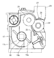
図1に示すように、本実施形態に係る画像形成装置は、像担持体ユニットまたはプロセスユニットとしての4色分の作像装置15Y(イエロー)、15M(マゼンタ)、15C(シアン)、15K(黒)を有しており、各ステーションとしての作像装置15は装置本体80に対して着脱自在に設けられている。
各作像装置15の他に、レーザ光を照射可能な露光手段としての光走査装置20、中間転写体ユニット30、給紙ユニット60、及び定着手段としての定着ユニット50等を備えている。
Embodiments of the present invention will be described below with reference to the drawings.
The first embodiment will be described with reference to FIGS. First, an outline of the configuration of an image forming apparatus capable of full color image formation according to the present embodiment will be described with reference to FIG.
As shown in FIG. 1, the image forming apparatus according to the present embodiment includes
In addition to each
各作像装置15Y、15C、15M、15Kの構造は現像色が異なるだけで同一である。イエローの作像装置15Yを代表して説明すると、それぞれ像担持体としての感光体ドラム9Yと、感光体ドラムを帯電する帯電装置13Yと、感光体ドラムに残留した現像剤等を除去するクリーニング装置14Yと、感光体ドラムに形成された潜像を現像する現像装置16Yとを一体に備えている。
また、各作像装置は、装置本体の操作面側に設けられた図示しない開閉式面板の開閉方向、すなわち感光体ドラムの回転軸方向に装置本体に対して着脱自在な構成になっている。
The structures of the
Each image forming apparatus is configured to be detachable from the apparatus main body in the opening / closing direction of an openable / closable face plate (not shown) provided on the operation surface side of the apparatus main body, that is, the rotation axis direction of the photosensitive drum.
中間転写体ユニット30は、中間転写体としての無端状の転写ベルト31と、各感光体ドラム9に形成されたトナー像を転写ベルト31に転写する一次転写手段としての4本の一次転写ローラ35と、転写ベルト31上に転写されたトナー像を更に記録媒体としての記録紙Pに転写する二次転写手段としての二次転写ローラ36とを備えている。
転写ベルト31は、支持ローラ32、33、一次転写ローラ35間に掛け回されており、支持ローラ32は転写ベルト31を挟んで二次転写ローラ36と対向し、二次転写ローラ36との間で二次転写ニップ部を形成している。
支持ローラ33に対向する部位には、転写後の転写ベルト31の表面をクリーニングするベルトクリーニング装置38が設けられている。
The intermediate
The
A
給紙ユニット60は、図示しない上昇モータにて給紙カセット41内部に設置したアーム48を稼動させてトレイ底板47を上昇させることで、記録紙Pの束を呼び出しコロ61に当接させる構成を有している。
呼び出しコロ61を回転させることによって記録紙Pの束を給紙方向下流にずらし、給紙コロ62と逆転コロ63とによって最上紙の一枚を分離し、搬送コロ対64、レジストローラ対65によって二次転写領域に搬送する。
定着ユニット50は、定着ローラ51及び加圧ローラ52を備え、記録紙P上のトナー像に熱と圧を加えることで定着を行う。
The
By rotating the
The
上記構成において、まず1色目のイエローの作像装置15Yにおいて、感光体ドラム9が帯電装置13によって一様に帯電された後、光走査装置20から照射されたレーザ光(イエローの画像データで変調された光ビーム)によって静電潜像が形成され、該潜像は現像装置16によってトナー像として可視像化される。
感光体ドラム9上に形成されたトナー像は、一次転写ローラ35の作用によって転写ベルト31上に転写される。一次転写が終了した感光体ドラム12はクリーニング装置14によってクリーニングされ、次の画像形成に備える。
クリーニング装置14によって回収された残留トナーは、作像装置の取り出し方向に設置された図示しない廃トナー回収ボトルに貯蔵される。この廃トナー回収ボトルは満杯になると交換できるように装置本体に対し着脱自在になっている。
In the above configuration, first, in the yellow
The toner image formed on the photosensitive drum 9 is transferred onto the
The residual toner collected by the cleaning device 14 is stored in a waste toner collection bottle (not shown) installed in the take-out direction of the image forming device. The waste toner collection bottle is detachable from the apparatus main body so that it can be replaced when it is full.
同様の画像形成工程が作像装置15M、15C、15Kにおいても行われて各色のトナー像が形成され、先に形成されたトナー像に順次重ねてフルカラー画像として転写される。
一方、記録紙Pが給紙カセット41から二次転写領域に搬送され、転写バイアスが印加される二次転写ローラ36によって転写ベルト31上に形成されたトナー像が記録紙Pに二次転写される。
トナー像を転写された記録紙Pは定着ユニット50に搬送され、該定着ユニット50の定着ローラ51と加圧ローラ52とのニップ部にてトナー像が定着され、排紙ローラ対55によって排紙トレイ56に排紙される。
手差しトレイ59にも記録紙Pがセットされており、給紙ローラ58にて同様に給紙・搬送されるとともに、転写、定着され、排紙トレイ56に排出される。
画像形成によって各作像装置15Y、15M、15C、15Kのトナーは消費される。これに応じて新しいトナーがトナーボトル57Y、57M、57C、57Kから補給される。トナー補給時には、トナーボトル57Y、57M、57C、57Kが回転され、図示しないパイプを通してトナーが各作像装置に搬送される。
A similar image forming process is also performed in the
On the other hand, the recording paper P is conveyed from the paper feed cassette 41 to the secondary transfer region, and the toner image formed on the
The recording paper P to which the toner image has been transferred is conveyed to the fixing
The recording paper P is also set on the
The toner of each
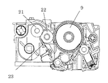
図2は、各作像装置の詳細図である。現像装置16は作像装置(プロセスユニット)15の一構成要素として感光体ドラム9等と一体に構成されている。
FIG. 2 is a detailed view of each image forming apparatus. The developing
図3に基づいて、本実施形態に係る現像装置16の構成及び現像装置内でのトナー挙動について説明する。
まず、ケーシング17のトナー収容部17aに収容されている現像剤としてのトナー(非磁性一成分現像剤)は、撹拌部材としての撹拌パドル18により、現像剤供給部材としての供給ローラ21に運ばれる。なお、本実施形態では、供給ローラ21を現像剤担持体としてのフレアローラ22とカウンタ方向に回転させることによって、供給ローラ21に回収ローラとしての機能も持たせている。もちろん供給部材と回収部材が独立していても良い。
供給ローラ21からフレアローラ22にトナーが供給されると、トナーはフレアローラおよび供給ローラとの摩擦により帯電される。帯電されたトナーは、フレアローラ内部の2相電極間の時間周期的に変化する電界に従ってホッピング運動(後述)を行う。
そして、フレアローラ自体の回転駆動によりトナー層厚規制部材23を通過して付着量が規制された後、感光体ドラム9との対向領域(現像領域)に搬送され、感光体ドラム上の静電潜像を非接触で現像する。
Based on FIG. 3, the configuration of the developing
First, toner (nonmagnetic one-component developer) as a developer accommodated in the
When toner is supplied from the
Then, after the flare roller itself rotates and passes through the toner layer
一方、現像に寄与しなかったトナーは、現像領域を通過する。通過後のトナーは、回収ローラとしての機能も有する供給ローラ21で回収され、トナー収容部17aに一旦戻される。フレアローラ上のトナーはホッピングしているため、フレアローラとトナーの付着力は小さく、回収ローラで容易に回収される。
上記の一連のプロセスを繰り返すことによってフレアローラ上には常にトナーがホッピングしている状態が形成される。
シール部材26は、ケーシング17を構成する要素25に一端部を固定され、自由端部はフレアローラ22の回転方向に沿うようにフレアローラ22の表面に接触している。
On the other hand, the toner that has not contributed to development passes through the development area. The toner after passing is collected by the
By repeating the above-described series of processes, a state where toner is always hopping is formed on the flare roller.
One end of the sealing
上述のように、対向領域下流でシール部材26がフレアローラ22と当接する場合、フレアローラ上でホッピングしているトナーはフレアローラとの付着力が小さいためシール部材26ではじかれてしまい通過することができないことが問題となる。
本実施形態ではこれを解消すべく、現像残トナーを供給ローラ21により回収する位置よりも、フレアローラ22の回転方向上流側に、現像残トナーに帯電を付与する帯電付与手段としてのローラ状の帯電付与部材27を設けている。
帯電付与部材27には図示しない電圧印加手段が接続されている。現像残トナーに対して帯電付与部材27により電荷を付与し、フレアローラ22による拘束力が高まるように帯電量を高くすることで、トナー飛散を抑制することができる。
As described above, when the
In the present embodiment, in order to solve this problem, a roller-shaped roller serving as a charge applying unit for applying charge to the development residual toner is provided upstream of the position where the development residual toner is collected by the
A voltage applying means (not shown) is connected to the
本実施形態ででは、フレアローラ内部の2相の電極に印加するバイアスとして図11(b)に示すような矩形波を用いた。すなわち、2相の電極ともオフセット電圧V0が-300Vで、周波数fが700Hz、ピークツーピーク電圧Vppが500Vの矩形波バイアスとした。
帯電付与部材27は、ゴムで形成されたローラであり、フレアローラに対して1mmギャップを隔てて設置している。また、帯電付与部材27は図示しない回転機構により回転される。回転はフレアローラ表面と帯電付与部材27の表面の速度が等しくなる回転数で駆動させた。
帯電付与部材27には、交流電圧を印加して効果を検証した。印加したバイアスは、-2kVpp,1kHzのサイン波でオフセット値を変えながら、現像後トナーのQ/M(帯電量)および飛散量を測定した。
In this embodiment, a rectangular wave as shown in FIG. 11B is used as a bias applied to the two-phase electrodes inside the flare roller. That is, the two-phase electrodes were each a rectangular wave bias having an offset voltage V0 of −300V, a frequency f of 700 Hz, and a peak-to-peak voltage Vpp of 500V.
The charging
The effect was verified by applying an AC voltage to the charging
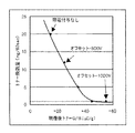
図4に検証結果を示す。縦軸のトナー飛散量は、現像装置を紙で覆い、紙に付着するトナー量を計測した。図から分かるように、現像後のトナーQ/Mが上がると、トナー飛散量は低減する。
これは、Q/Mが上がることで、トナー1個1個の帯電量が上がり、フレアローラに印加されている電界による拘束力が上がるためである。また、Q/Mが-50uC/g以上となる場合には、トナー1個1個の帯電も非常に高く、フレアローラとトナーとの間の静電付着力が高くなるために、ホッピングできなくなり、結果としてフレアローラに密着した状態(拘束力が極限まで上がった状態)でシール部へ進入するために、トナー飛散量は低減する。
FIG. 4 shows the verification result. The amount of toner scattering on the vertical axis was measured by covering the developing device with paper and the amount of toner adhering to the paper. As can be seen from the figure, as the toner Q / M after development increases, the amount of toner scattering decreases.
This is because as the Q / M increases, the charge amount of each toner increases, and the binding force due to the electric field applied to the flare roller increases. In addition, when Q / M is -50uC / g or more, the charge of each toner is very high, and the electrostatic adhesion between the flare roller and the toner becomes high, so it is impossible to hop. As a result, since the toner enters the seal portion in a state of being in close contact with the flare roller (in a state where the restraining force is increased to the limit), the amount of scattered toner is reduced.
図中、点線で示した飛散量は、市販されている現像装置(現像ローラや磁性キャリアに吸着させたトナーを現像に用いる方式)で測定した結果であり、オフセット値を上げることで、フレア方式において市場機同等レベルまで改善可能であることを確認できた。
本実施形態ではローラ状の帯電付与部材27を回転させる構成としたが、固定方式としても帯電付与機能は得ることができる。回転方式とした場合、フレアローラ22に対向する帯電付与部材27の放電面を常にクリアにすることができ、帯電機能を均一に維持することができる利点を有している。
図示していないが、帯電付与部材としては、ローラ形状に限定されるものではなく、ワイヤ形状でも同等の効果を得ることができる。
In the figure, the amount of scattering shown by the dotted line is the result of measurement with a commercially available developing device (method that uses toner adsorbed on a developing roller or magnetic carrier for development). By increasing the offset value, the flare method It was confirmed that it can be improved to the same level as the market.
In the present embodiment, the roller-shaped
Although not shown, the charging member is not limited to a roller shape, and the same effect can be obtained even in a wire shape.
図3に示した現像装置では、現像上シール部材としてのマイラー(登録商標)からなるシール部材26を、フレアローラの鉛直方向における頂点の位置で接触するように設置しているが、重力の影響を考えると、跳ね返ったものが再びシール部に進入するようなレイアウトが望ましい。
すなわち、フレアローラ22の表面の鉛直方向における最も高い位置(図3に示す位置)に対して、該位置よりもフレアローラ22の回転方向下流側で且つ低い位置で接触するように設けることが望ましい。
In the developing device shown in FIG. 3, the
That is, it is desirable that the
図5に基づいて第2の実施形態を説明する。なお、上記実施形態と同一部分は同一符号で示し、特に必要がない限り既にした構成上及び機能上の説明は省略して要部のみ説明する。
本実施形態では、現像残トナーが装置内に進入する部位に、フレアローラ22の表面との間にギャップを介して入口部材29が設けられている。これにより、フレアローラ22と入口部材29との間には、現像残トナーを装置内に誘導する搬送路25が形成されている。
搬送路25は、フレアローラ22の表面に沿った円弧状の断面形状を有し、フレアローラ22に対して非接触の開口部ともいうべきものである。
入口部材29には、搬送路25に臨むようにローラ状の帯電付与部材27が設けられている。帯電付与部材27は上記のように回転するように設けてもよく、ワイヤ形状としてもよい。
本実施形態では、閉鎖的な空間である搬送路25によりフレアローラ22の回転に伴う引き込み気流により現像残トナーを装置内に取り込むことができ、且つ、帯電付与部材27による拘束力を得ることができるので、シール部材26は設けられていない。
A second embodiment will be described with reference to FIG. In addition, the same part as the said embodiment is shown with the same code | symbol, and unless it was especially required, the description on the structure and function which were already demonstrated is abbreviate | omitted, and only the principal part is demonstrated.
In the present embodiment, an
The
The
In the present embodiment, the undeveloped toner can be taken into the apparatus by the drawing air flow accompanying the rotation of the
フレアローラ22の回転による引き込み気流で現像残トナーはトナー収容部に運ばれるが、搬送路25を設けただけの構成では、トナー収容部側の内圧の上昇により吐き出し気流が発生し、図10で示したシール部材26による接触構成と同様に、トナーがはじかれて飛散が発生してしまう。
帯電付与部材27を設けることにより、搬送路25を有する構成においてもトナー飛散を抑制することができる。
The undeveloped toner is carried to the toner accommodating portion by the drawing airflow caused by the rotation of the
By providing the
表1は、フレアローラ22の鉛直方向の頂点にてシール部材26がローラに当接する条件(図3)、シール部材の当接位置をフレアローラ22の回転方向下流側の低い位置にした条件(請求項5)、非接触の開口としての搬送路25を備えた条件(図5)のそれぞれについて、帯電付与部材有無でのトナー飛散量の計測結果を示している。
帯電付与部材の効果はいずれの形態においても現れ、搬送路(非接触開口)との組み合わせによってさらに飛散量が低減することが確認された。
シール部材の当接位置をフレアローラ22の回転方向下流側の低い位置にした条件では、帯電付与部材を設けた場合、頂点位置でシールする場合と同様の結果となったが、下流側の低い位置でのシール構成では、それ自体で帯電付与部材が無い場合の飛散抑制効果があるため、トナー飛散を確実に抑制する観点からは、シール位置を重力による再進入機能が得られる「下流側の低い位置でのシール構成」と帯電付与部材との組み合わせが望ましい。
Table 1 shows a condition in which the
It was confirmed that the effect of the charge imparting member appeared in any form, and the amount of scattering was further reduced by the combination with the conveyance path (non-contact opening).
Under the condition that the contact position of the seal member is set to a low position on the downstream side in the rotation direction of the

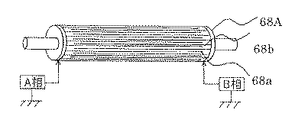
以下にフレア現像について説明する。
フレアローラ22の概略図を図6に示す。図7はフレアローラの電極部分の周方向断面の概略図である。
支持基板上に電極が所定の間隔で配置され、その上に無機又は有機の絶縁性材料で形成した表面保護層が積層されている。なお、図7において各電極から伸びる線は各電極に電圧を印加するための導電線を表しており、各線の重なる部分のうち黒丸で示した部分だけが電気的に接続されており、他の部分は電気的に絶縁状態である。
各電極に対しては、本体側の電源から2相の異なる駆動電圧が印加される。
The flare development will be described below.
A schematic view of the
Electrodes are arranged on the support substrate at predetermined intervals, and a surface protective layer made of an inorganic or organic insulating material is laminated thereon. In addition, the line extended from each electrode in FIG. 7 represents the conductive wire for applying a voltage to each electrode, and only the part shown by the black circle among the overlapping parts of each line is electrically connected, The part is electrically insulated.
Two-phase different drive voltages are applied to each electrode from the power source on the main body side.
図8はフレアローラ電極部の平面展開図である。これらの図からわかるように、フレアローラは、トナーをホッピングさせるための電界を発生する2相の電極群を有し、偶数番目の電極群と奇数番目の電極群にそれぞれ図示しない駆動回路から一例としては図9(a)もしくは(b)に示すような逆位相の駆動波形が印加され、2相の電極間に時間周期的な電位差が形成される。
そしてフレアローラは回転駆動され、回転軸の一方に奇数番電極が接続され、回転軸のもう一方に偶数番電極が接続されている。
FIG. 8 is a plan development view of the flare roller electrode portion. As can be seen from these figures, the flare roller has a two-phase electrode group that generates an electric field for hopping the toner, and an example is shown in each of the even-numbered electrode group and the odd-numbered electrode group from drive circuits (not shown). As shown in FIG. 9 (a) or (b), an antiphase driving waveform is applied, and a time-periodic potential difference is formed between the two-phase electrodes.
The flare roller is rotationally driven, and an odd numbered electrode is connected to one of the rotating shafts, and an even numbered electrode is connected to the other of the rotating shafts.
フレアローラの支持基板としては、樹脂等の絶縁性材料、あるいはSUS等の導電性材料からなる基板にSiO2等の絶縁膜を成膜したもの等を適用できる。
電極は、支持基板上に、Al、Cu、Ni-Cr等の導電性材料を0.1〜10um厚、好ましくは0.5〜2.0umで成膜し、これをフォトリソ技術等で所要の電極形状にパターニングして形成している。
As the support substrate of the flare roller, an insulating material such as a resin, or a substrate made of a conductive material such as SUS and an insulating film such as SiO 2 may be applied.
The electrode is formed on a support substrate with a conductive material such as Al, Cu, Ni-Cr, etc. in a thickness of 0.1 to 10 um, preferably 0.5 to 2.0 um, and this is patterned into the required electrode shape using photolithography technology or the like. Formed.
次にトナーのホッピングを行うためのフレアローラ上の電極幅L及び電極間隔R、駆動波形形状並びに表面保護層について説明する。
搬送部材における電極幅Lと電極間隔Rはトナーのホッピング効率に大きく影響する。なお電極ピッチPは、P=R+Lで表される。
電極と電極の間にあるトナーはほぼ水平方向の電界により、基板表面を隣接する電極まで移動する。これに対して、電極上に乗っているトナーは、少なくとも垂直方向の成分も持った初速が与えられることから、多くは基板面から離れて飛翔する。
特に、電極端面付近にあるトナーは、隣接電極を飛び越えて移動するため、電極幅Lが広い場合には、その電極上に乗っているトナーの数が多くなり、移動距離の大きいトナーが増える。
Next, the electrode width L and electrode interval R on the flare roller for toner hopping, the drive waveform shape, and the surface protective layer will be described.
The electrode width L and the electrode interval R in the conveying member greatly affect the toner hopping efficiency. The electrode pitch P is expressed by P = R + L.
The toner between the electrodes moves to the adjacent electrode on the substrate surface by a substantially horizontal electric field. On the other hand, since the toner on the electrode is given an initial velocity having at least a component in the vertical direction, most of the toner flies away from the substrate surface.
In particular, since the toner near the electrode end surface moves over the adjacent electrode, when the electrode width L is wide, the number of toners on the electrode increases, and the toner having a large moving distance increases.
但し、電極幅Lが広すぎると、電極中央付近の電界強度が低下するためにトナーが電極に付着し、ホッピング効率が低下することになる。
そこで、本発明者らは鋭意研究した結果、低電圧で効率よくトナーをホッピングさせるための適正な電極幅があることを見出した。
また、電極間隔Rは、距離と印加電圧の関係から電極間の電界強度を決定し、間隔Rが狭い程電界強度は当然強く、ホッピングの初速が得られやすい。しかし、電極から電極へ移動するようなトナーについては、一回の移動距離が短くなり、駆動周波数を高くしないとホッピングしている時間が短くなり、着地している時間が長くなる。これについても、本発明者らは鋭意研究した結果、低電圧で効率よくトナーを搬送、ホッピングするための適正な電極間隔があることを見出した。
さらに、電極表面を覆う表面保護層の厚さも電極表面の電界強度に影響を与え、特に垂直方向成分の電気力線への影響が大きく、ホッピングの効率を決定することをも見出した。
However, if the electrode width L is too wide, the electric field strength in the vicinity of the center of the electrode is lowered, so that the toner adheres to the electrode and the hopping efficiency is lowered.
Therefore, as a result of intensive studies, the present inventors have found that there is an appropriate electrode width for efficiently hopping toner at a low voltage.
In addition, the electrode interval R determines the electric field strength between the electrodes from the relationship between the distance and the applied voltage. The smaller the interval R, the stronger the electric field strength, and the easier the initial hopping speed is obtained. However, toner that moves from electrode to electrode has a short moving distance, and unless the drive frequency is increased, the hopping time is shortened and the landing time is lengthened. As a result of intensive studies, the present inventors have found that there is an appropriate electrode interval for efficiently transporting and hopping toner at a low voltage.
Further, the present inventors have also found that the thickness of the surface protective layer covering the electrode surface also affects the electric field strength on the electrode surface, in particular, the influence of the vertical component on the electric field lines is large, and determines the hopping efficiency.
すなわち、フレアローラの電極幅、電極間隔、表面保護層厚さの関係を適正に設定することによって、低電圧で効率的なホッピングを行うことができる。
そこで、上記各実施形態では、図7に示す電極幅Lは、トナー平均粒径の1倍以上20倍以下とし、かつ、電極間隔Rもトナー平均粒径の1倍以上20倍以下としている。
次に、表面保護層は、例えばSiO2、BaTiO2、TiO2、TiO4、SiON、BN、TiN、Ta2O5等を適用でき、厚さは0.5〜30umで形成している。
また、SiO2等の上にポリカなどの有機材料をコートしても良い。ジルコニア、あるいは二成分現像剤のキャリアのコート材料として一般的に使われる材料、例えばシリコーン系樹脂を選択することもできる。表面保護層は、絶縁性、耐久性、フレアローラ自体の製法、及び使用するトナーとの帯電列との関係から適宜選択される。
That is, by appropriately setting the relationship between the electrode width of the flare roller, the electrode interval, and the surface protective layer thickness, efficient hopping can be performed at a low voltage.
Therefore, in each of the above embodiments, the electrode width L shown in FIG. 7 is 1 to 20 times the average toner particle size, and the electrode interval R is also 1 to 20 times the average toner particle size.
Next, for example, SiO 2 , BaTiO 2 , TiO 2 , TiO 4 , SiON, BN, TiN, Ta 2 O 5 or the like can be applied to the surface protective layer, and the thickness is formed to be 0.5 to 30 μm.
Further, an organic material such as polycarbonate may be coated on SiO 2 or the like. It is also possible to select zirconia or a material generally used as a coating material for a carrier of a two-component developer, for example, a silicone resin. The surface protective layer is appropriately selected from the relationship between the insulating property, durability, the production method of the flare roller itself, and the charge train with the toner to be used.
本発明に係る現像装置を画像形成装置に用いる場合、フレアローラとして、少なくともA4縦幅21cm、または横幅30cm以上の長尺、大面積にファインパターンの実用が必要になってくる。
ここでフレアローラの製法についていくつか挙げる。
まず、初めに、フレキシブルな電極パターンを形成し、それを支持ドラムに巻き付けてフレアローラを形成する場合について説明する。
フレキシブルなファインピッチ薄層電極を有する基板の一例としては、ポリイミドのベースフィルム(厚さ20〜100um)を基材(支持基板)として、その上に蒸着法によって0.1〜0.3umのCu、Al、Ni-Cr等を成膜する。幅30〜60cmであれば、ロール・トゥ・ロールの装置で製造可能であり、量産性が非常に高まる。共通バスラインは同時に幅1〜5mm程度の電極を形成する。
When the developing device according to the present invention is used in an image forming apparatus, it is necessary to use a fine pattern as a flare roller that is at least as long as
Here are some examples of how to make flare rollers.
First, a case where a flexible electrode pattern is formed and wound around a support drum to form a flare roller will be described.
As an example of a substrate having a flexible fine pitch thin layer electrode, a polyimide base film (
この蒸着法の具体的手段としては、スパッタ法、イオンプレーティング法、CVD法、イオンビーム法、等の方法が可能である。例えば、スパッタ法で電極を形成する場合において、ポリイミドとの密着性を向上させるため、Cr膜を介在させても良いし、プラズマ処理やプライマー処理によっても密着性を向上させることができる。 As a specific means of the vapor deposition method, a sputtering method, an ion plating method, a CVD method, an ion beam method, or the like can be used. For example, when an electrode is formed by sputtering, a Cr film may be interposed in order to improve the adhesion with polyimide, and the adhesion can also be improved by plasma treatment or primer treatment.
蒸着法以外の工法としては、電着法によっても薄層電極を形成することができる。この場合は、前記ポリイミドの基材上に、まず、無電解メッキによって電極を形成する。塩化Sn、塩化Pd、塩化Niに順次浸漬して下地電極を形成した後、Ni電解液中で電解メッキを行ってNi膜1〜3umをロール・トゥ・ロールで製造することが可能である。
これらの薄膜電極にレジスト塗布、パタンニング、エッチングで電極12を形成する。この場合、0.1〜3um厚さの薄層電極であれば、フォトリソ、エッチング処理によって5um〜数10um幅、又は間隔のファインパターン電極を精度良く形成することができる。
As a method other than the vapor deposition method, the thin layer electrode can be formed also by an electrodeposition method. In this case, an electrode is first formed on the polyimide substrate by electroless plating. After the base electrode is formed by sequentially immersing in Sn chloride, Pd chloride, and Ni chloride, the Ni film of 1 to 3 um can be manufactured roll-to-roll by electrolytic plating in a Ni electrolyte solution.
Electrodes 12 are formed on these thin film electrodes by resist coating, patterning, and etching. In this case, if it is a thin layer electrode having a thickness of 0.1 to 3 μm, a fine pattern electrode having a width of 5 μm to several tens of μm or an interval can be accurately formed by photolithography and etching.
次いで、表面保護層13としてSiO2 、BaTiO2、TiO2 等を厚さ0.5〜2umをスパッタ等により形成する。或いは、表面保護層としてPI(ポリイミド)を厚さ2〜5μmにロールコータ、その他コーティング装置により塗布し、ベークして仕上げる。PIのままで支障を生じるときには、更に最表面にSiO2 、その他無機膜を0.1〜0.5umの厚みにスパッタ等で形成すればよい。また、SiO2等の上にポリカなどの有機材料をコートしても良い。ジルコニア、あるいは二成分現像剤のキャリアのコート材料として一般的に使われる材料、例えばシリコーン系樹脂を選択することもできる。 Next, SiO 2 , BaTiO 2 , TiO 2 or the like is formed as the surface protective layer 13 to a thickness of 0.5 to 2 μm by sputtering or the like. Alternatively, PI (polyimide) as a surface protective layer is applied to a thickness of 2 to 5 μm with a roll coater or other coating apparatus, and baked to finish. When trouble occurs with PI, it is sufficient to form SiO 2 on the outermost surface and other inorganic film to a thickness of 0.1 to 0.5 μm by sputtering or the like. Further, an organic material such as polycarbonate may be coated on SiO 2 or the like. It is also possible to select zirconia or a material generally used as a coating material for a carrier of a two-component developer, for example, a silicone resin.
このようなフレキシブル基板を構成することによって、円筒形状のドラムに貼り付けたり、或いは、部分的に曲面形状にしたりすることが容易に行える。
別の例としては、ポリイミドのベースフィルム(厚さ20〜100um)を基材(支持基板)として、その上に電極材料として、厚さ10〜20umのCu、SUS等を使用することも可能である。この場合は、逆に金属材の上にポリイミドをロールコータにて20〜100um塗布してベークする。その後、金属材をフォトリソ、エッチング処理によって電極の形状にパターン化し、その電極面上に保護層13としてポリイミドをコーティング、金属材電極の厚さ10〜20umに応じた凹凸がある場合は平坦化して完成する。
By configuring such a flexible substrate, it can be easily attached to a cylindrical drum, or partially curved.
As another example, it is also possible to use 10 to 20um thick Cu, SUS, etc. as a base material (supporting substrate) with a polyimide base film (
例えば、粘度50〜10,000cps、より好ましくは100〜300cpsのポリイミド系材料、ポリウレタン系材料をスピンコートして放置することによって、材料の表面張力によって基板の凹凸がスムージングされ、搬送部材最表面が平坦化される。
フレキシブル基板の強度を上げた更に他の例としては、基材として厚さ20〜30umのSUS、Al基材等を用いて、その表面に絶縁層(電極と基材との間の絶縁)として5um程度の希釈したポリイミド材をロールコータによりコーティングする。そして、このポリイミドを例えば150℃−30分のプリベーク、350℃−60分のポストベークして薄層ポリイミド膜を形成して支持基板とする。
For example, when a polyimide material or polyurethane material having a viscosity of 50 to 10,000 cps, more preferably 100 to 300 cps, is spin-coated and left standing, the unevenness of the substrate is smoothed by the surface tension of the material, and the outermost surface of the conveying member is flat. It becomes.
As yet another example of increasing the strength of the flexible substrate, a 20-30 um thick SUS or Al base material is used as the base material, and an insulating layer (insulation between the electrode and the base material) is formed on the surface. The diluted polyimide material of about 5um is coated with a roll coater. Then, this polyimide is pre-baked, for example, at 150 ° C. for 30 minutes, and post-baked at 350 ° C. for 60 minutes to form a thin-layer polyimide film to be a support substrate.
その後、密着性向上のプラズマ処理やプライマー処理を施した後、薄層電極層としてNi-Crを0.1〜0.2umの厚みに蒸着し、フォトリソ、エッチングによって前記数10umのファインパターンの電極12を形成する。さらに、表面に前記SiO2、BaTiO2、TiO2 等の表面保護層を0.5〜1μm程度の厚みにスパッタにより形成することで、フレキシブル搬送部材を得ることができる。
また、SiO2等の上にポリカなどの有機材料をコートしても良い。ジルコニア、あるいは二成分現像剤のキャリアのコート材料として一般的に使われる材料、例えばシリコーン系樹脂を選択することもできる。
別のフレアローラの製法としては、導電インクを用いたスクリーン印刷、インクジェットによるプリント、メッキ加工した電極の非電極部をレーザ加工で除去する等の製法も挙げられるが、電極パターンおよび表面保護層の作成方法は上述の方法に限定されるものではない。
Then, after performing plasma treatment and primer treatment for improving adhesion, Ni-Cr is deposited as a thin electrode layer to a thickness of 0.1 to 0.2 um, and the fine pattern electrode 12 of several tens um is formed by photolithography and etching. To do. Furthermore, a flexible transport member can be obtained by forming a surface protective layer of SiO 2 , BaTiO 2 , TiO 2 or the like on the surface to a thickness of about 0.5 to 1 μm by sputtering.
Further, an organic material such as polycarbonate may be coated on SiO 2 or the like. It is also possible to select zirconia or a material generally used as a coating material for a carrier of a two-component developer, for example, a silicone resin.
Other flare roller manufacturing methods include screen printing using conductive ink, ink-jet printing, and other methods such as removing non-electrode parts of the plated electrode by laser processing. The creation method is not limited to the above-described method.
9 像担持体としての感光体ドラム
16 現像装置
21 現像剤供給部材としての供給ローラ
22 現像剤担持体としてのフレアローラ
25 搬送路
26 シール部材
27 帯電付与手段としての帯電付与部材
29 入口部材
DESCRIPTION OF SYMBOLS 9 Photosensitive drum as
Claims (7)
前記現像剤担持体に現像剤を供給する現像剤供給部材と、
を有し、
前記現像剤担持体は、第一の電極と、第一の電極に対して絶縁体を介して設けられた第二の電極とを備え、
第一の電極及び第二の電極間の電位差が時間的に反転する電圧を印加することで前記現像剤担持体上の現像剤をクラウド化し、前記現像剤担持体の表面が移動することによって現像剤を現像領域へ搬送して前記像担持体に形成された静電潜像を現像し、現像後に前記現像剤担持体上に残った現像剤を前記現像剤供給部材にて回収する現像装置において、
前記現像後に残った現像剤を前記現像剤供給部材により回収する位置よりも、前記現像剤担持体の回転方向上流側に、前記現像後に残った現像剤に帯電を付与する帯電付与手段を設けたことを特徴とする現像装置。 A developer carrier for conveying the developer to the image carrier;
A developer supply member for supplying a developer to the developer carrier;
Have
The developer carrier includes a first electrode and a second electrode provided via an insulator with respect to the first electrode,
The developer on the developer carrier is clouded by applying a voltage at which the potential difference between the first electrode and the second electrode is reversed in time, and the developer is developed by moving the surface of the developer carrier. In a developing device for transporting a developer to a development region to develop an electrostatic latent image formed on the image carrier and collecting the developer remaining on the developer carrier after development by the developer supply member ,
A charge imparting means for imparting a charge to the developer remaining after the development is provided on the upstream side in the rotation direction of the developer carrier from the position where the developer remaining after the development is collected by the developer supply member. A developing device.
前記帯電付与手段が、前記現像剤担持体との間にギャップを介して配置されたローラ状部材で構成されていることを特徴とする現像装置。 The developing device according to claim 1,
2. A developing apparatus according to claim 1, wherein said charging means is constituted by a roller-like member disposed with a gap between said developer-carrying member and said developer-carrying member.
前記ローラ状部材が回転することを特徴とする現像装置。 The developing device according to claim 2,
A developing device in which the roller-like member rotates.
前記帯電付与手段が、前記現像剤担持体との間にギャップを介して配置され、前記現像剤担持体の軸方向に張られたワイヤであることを特徴とする現像装置。 The developing device according to claim 1,
2. A developing apparatus according to claim 1, wherein said charging means is a wire disposed in a gap with said developer carrying member and extending in the axial direction of said developer carrying member.
前記現像後に残った現像剤が装置内に進入する際、装置の内側と外側とを遮るシール部材を備え、
前記シール部材は、前記現像剤担持体の表面の鉛直方向における最も高い位置に対して、該位置よりも前記現像剤担持体の回転方向下流側で且つ低い位置に設けられていることを特徴とする現像装置。 In the developing device according to any one of claims 1 to 4,
A seal member that shields the inside and outside of the apparatus when the developer remaining after the development enters the apparatus;
The seal member is provided at a position downstream and lower in the rotation direction of the developer carrier than the highest position in the vertical direction of the surface of the developer carrier. Developing device.
前記現像後に残った現像剤が装置内に進入する部位に、前記現像剤担持体の表面との間にギャップを介して入口部材が設けられ、前記現像担持体と前記入口部材との間に、前記現像後に残った現像剤を装置内に誘導する搬送路が形成されていることを特徴とする現像装置。 In the developing device according to any one of claims 1 to 4,
An inlet member is provided through a gap between the surface of the developer carrier at a portion where the developer remaining after the development enters the apparatus, and between the developer carrier and the inlet member, A developing device characterized in that a conveying path for guiding the developer remaining after the development into the device is formed.
前記現像装置が、請求項1〜6のいずれか1つに記載のものであることを特徴とする画像形成装置。 In an image forming apparatus that visualizes an electrostatic latent image formed on an image carrier based on image information as a toner image by a developing device, and finally transfers the toner image to a recording material to form an image.
7. The image forming apparatus according to claim 1, wherein the developing device is one according to any one of claims 1 to 6.
Priority Applications (1)
| Application Number | Priority Date | Filing Date | Title |
|---|---|---|---|
| JP2012067582A JP2013200375A (en) | 2012-03-23 | 2012-03-23 | Developing device and image forming apparatus |
Applications Claiming Priority (1)
| Application Number | Priority Date | Filing Date | Title |
|---|---|---|---|
| JP2012067582A JP2013200375A (en) | 2012-03-23 | 2012-03-23 | Developing device and image forming apparatus |
Publications (1)
| Publication Number | Publication Date |
|---|---|
| JP2013200375A true JP2013200375A (en) | 2013-10-03 |
Family
ID=49520684
Family Applications (1)
| Application Number | Title | Priority Date | Filing Date |
|---|---|---|---|
| JP2012067582A Pending JP2013200375A (en) | 2012-03-23 | 2012-03-23 | Developing device and image forming apparatus |
Country Status (1)
| Country | Link |
|---|---|
| JP (1) | JP2013200375A (en) |
-
2012
- 2012-03-23 JP JP2012067582A patent/JP2013200375A/en active Pending
Similar Documents
| Publication | Publication Date | Title |
|---|---|---|
| JP5067849B2 (en) | Developing device and image forming apparatus | |
| JP5067846B2 (en) | Developing device, process cartridge, and image forming apparatus | |
| JP5177649B2 (en) | Developing device, process unit, and image forming apparatus | |
| US9829851B2 (en) | Cleaning device and image forming apparatus including the same | |
| JP2010026333A (en) | Developing device, image forming apparatus, and process cartridge | |
| JP2008008929A (en) | Developing device and image forming apparatus having the same | |
| JP2008216790A (en) | Process cartridge and image forming apparatus | |
| JP5483142B2 (en) | Developing device and image forming apparatus | |
| JP5139921B2 (en) | Developing device and image forming apparatus having the same | |
| JP4610432B2 (en) | Image forming apparatus | |
| JP2013200375A (en) | Developing device and image forming apparatus | |
| JP2008076461A (en) | Toner conveying device, developing device, image forming apparatus, and process cartridge | |
| JP2013210436A (en) | Developing device and image forming apparatus | |
| JP2010020185A (en) | Developer carrier, developing device, and image forming device | |
| JP2013200379A (en) | Developing device and image forming apparatus | |
| JP2013195441A (en) | Developing device and image forming device including the same | |
| JP2008122794A (en) | Developing device, process unit, and image forming apparatus | |
| JP5114107B2 (en) | Developing device and image forming apparatus equipped with the same | |
| JP2013182100A (en) | Developing device and image forming apparatus | |
| JP2010230821A (en) | Toner suction device and image forming apparatus | |
| JP2014059469A (en) | Developing device and image forming apparatus | |
| JP5387983B2 (en) | Developing device and image forming apparatus | |
| JP4721421B2 (en) | Color image forming apparatus | |
| JP2013092581A (en) | Developing device, and image forming apparatus including the same | |
| JP2014056104A (en) | Developing device, image forming apparatus, and developing method |