JP2013200319A - Electron microscope system and pattern dimension measuring method using the same - Google Patents
Electron microscope system and pattern dimension measuring method using the same Download PDFInfo
- Publication number
- JP2013200319A JP2013200319A JP2013144124A JP2013144124A JP2013200319A JP 2013200319 A JP2013200319 A JP 2013200319A JP 2013144124 A JP2013144124 A JP 2013144124A JP 2013144124 A JP2013144124 A JP 2013144124A JP 2013200319 A JP2013200319 A JP 2013200319A
- Authority
- JP
- Japan
- Prior art keywords
- pattern
- information
- dimension
- electron microscope
- sample
- Prior art date
- Legal status (The legal status is an assumption and is not a legal conclusion. Google has not performed a legal analysis and makes no representation as to the accuracy of the status listed.)
- Pending
Links
Images


Landscapes
- Length-Measuring Devices Using Wave Or Particle Radiation (AREA)
Abstract
Description
本発明は半導体製造のリソグラフィー工程に用いられるフォトマスク、及びリソグラフィー工程後のウェーハを、電子顕微鏡で撮影したパターン画像を計測するパターン画像計測測システムに関する。 The present invention relates to a photomask used in a lithography process of semiconductor manufacturing and a pattern image measurement and measurement system that measures a pattern image obtained by photographing a wafer after the lithography process with an electron microscope.
半導体回路パターンの微細化に伴い、光露光装置の解像度は限界に達し、しシリコンウェーハ上に設計通りの回路パターンを形成するため,フォトマスクの設計データにあらかじめ補正パターンを入れて、仕上がりの形状をコントロールするOPC(Optical Proximity Correction)処理が頻繁に行われるようになりつつある。 With the miniaturization of semiconductor circuit patterns, the resolution of optical exposure equipment has reached its limit, and in order to form the circuit pattern as designed on the silicon wafer, a correction pattern is put in the photomask design data in advance, and the finished shape OPC (Optical Proximity Correction) processing for controlling the image is frequently performed.
OPCパターンの設計は,OPC処理を行ったフォトマスクパターンが、シリコンウェーハ上にどのように転写されるかを予測する、光露光シミュレーションに基づいて行われる。その検証,すなわち,ウェーハ上に設計通りの回路パターンが形成されたかを確認するためには,ウェーハに転写されたパターン(レジストパターン)を観察することが必要である。非特許文献1には,電子顕微鏡で撮像したウェーハ上のパターン(図2(a))に,設計データ(図2(b))を重ね合わせて表示する(図2(c))システムが開示されている。 The OPC pattern is designed based on a light exposure simulation that predicts how the photomask pattern subjected to the OPC process is transferred onto the silicon wafer. In order to verify this, that is, to confirm whether the designed circuit pattern is formed on the wafer, it is necessary to observe the pattern (resist pattern) transferred to the wafer. Non-Patent Document 1 discloses a system for displaying design data (FIG. 2B) superimposed on a pattern (FIG. 2A) on a wafer imaged with an electron microscope (FIG. 2A) (FIG. 2C). Has been.
また,特許文献1,特許文献2には,電子顕微鏡像からエッジを検出してパターン輪郭線を得,それと,設計データとを重ね合わせ,各パターン部位における両者の位置関係からパターン変形量を数値化する方法が開示されている。 In Patent Document 1 and Patent Document 2, an edge is detected from an electron microscope image to obtain a pattern outline, and this is overlaid with design data, and the amount of pattern deformation is numerically calculated from the positional relationship between the two at each pattern site. Is disclosed.
OPC処理の検証をより正確に行うためには,電子顕微鏡像から得られたパターン輪郭線が,試料の実際のパターンエッジ端に即したものであることが重要である。しかしながら,特許文献1,特許文献2においては,パターンエッジ端を正しく捉えることに関して,全く考慮されていない。 In order to verify the OPC process more accurately, it is important that the pattern contour line obtained from the electron microscope image conforms to the actual pattern edge end of the sample. However, in Patent Document 1 and Patent Document 2, no consideration is given to correctly capturing the edge of the pattern edge.
図3は特許文献1に開示されているエッジ検出方法である。二次電子顕微鏡像(SEM像)上では,エッジ部は明るい帯,ホワイトバンドとして表れるが、図3の方法によれば,概ねホワイトバンドの中心線(同図604参照)がエッジ点とされる。 FIG. 3 shows an edge detection method disclosed in Patent Document 1. On the secondary electron microscope image (SEM image), the edge portion appears as a bright band and a white band, but according to the method of FIG. 3, the center line of the white band (see FIG. 604) is generally set as the edge point. .
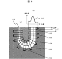
図4は特許文献2に開示されているエッジ検出方法である。図4(a)のプロファイル取得区間にて取得したプロファイルに対して,図4(b)のようにしきい値Tを与え,プロファイルとしきい値Tの交点(図ではQと表示)がエッジ点とされる。 FIG. 4 shows an edge detection method disclosed in Patent Document 2. A threshold value T is given to the profile acquired in the profile acquisition section of FIG. 4A as shown in FIG. 4B, and the intersection of the profile and the threshold value T (indicated by Q in the figure) is the edge point. Is done.
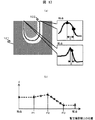
一方、非特許文献2に示されているように,対象パターンの断面形状によりSEM信号波形は変化する。図5(a)は,図2(a)に示したSEM画像の一部である。部位によってホワイトバンド幅が異なっているのは,部位によって試料の断面形状が異なることの現れであり,ホワイトバンド(図中の白い部分)の幅が狭い部位Aはエッジが切り立っていると推定され,ホワイトバンドの幅が広い部位Bはテーパを有している(エッジの傾きが比較的大きい)と推定される。図5(b)は部位A,部位Bに相当する部分のパターンの断面形状,及び,二次電子信号波形の模式図である。一般に,パターンエッジ端として捉えたいのは,パターンのボトム端(図中で検出したいエッジ端として示されている部分)であり,二次電子信号波形上では,黒丸を付した位置に相当する。 On the other hand, as shown in Non-Patent Document 2, the SEM signal waveform changes depending on the cross-sectional shape of the target pattern. FIG. 5A is a part of the SEM image shown in FIG. The white band width differs depending on the part, which is an indication that the cross-sectional shape of the sample differs depending on the part. The part A where the white band (white part in the figure) has a narrow width is estimated to have a sharp edge. , It is presumed that the portion B where the white band is wide has a taper (the inclination of the edge is relatively large). FIG. 5B is a schematic diagram of the cross-sectional shape of the pattern corresponding to the part A and the part B, and the secondary electron signal waveform. In general, what is desired to be regarded as the pattern edge end is the bottom end of the pattern (the portion indicated as the edge end that is desired to be detected in the figure), and corresponds to the black circled position on the secondary electron signal waveform.
しかしながら,特許文献1に記載されているパターンエッジ検出方式(図3)によれば,検出されるエッジ点はホワイトバンドの中心線なので,図5(c)の黒三角を付した位置となる。また,特許文献2に記載されているパターンエッジ検出方式(図4)によると,検出されるエッジ点は,しきい値Tに依存するが,例えばmaxとminの中点をしきい値とするならば,図5(d)の黒四角を付した位置となる。 However, according to the pattern edge detection method (FIG. 3) described in Patent Document 1, since the detected edge point is the center line of the white band, the position is indicated by the black triangle in FIG. 5 (c). Also, according to the pattern edge detection method described in Patent Document 2 (FIG. 4), the detected edge point depends on the threshold value T, but for example, the midpoint between max and min is set as the threshold value. Then, the black square in FIG.
図5(c)および(d)において図5(b)に黒丸で示したようなパターンのボトム端が検出されていないのは明らかである。さらに問題なのは,図5(c)および(d)において,検出されるエッジ点とパターンのボトム端との距離が,パターンの断面形状(図においては部位Aと部位B)によって異なるという点である。 In FIGS. 5C and 5D, it is apparent that the bottom end of the pattern as shown by the black circle in FIG. 5B is not detected. A further problem is that in FIGS. 5C and 5D, the distance between the detected edge point and the bottom end of the pattern differs depending on the cross-sectional shape of the pattern (part A and part B in the figure). .
図5(a)において部位によってホワイトバンド幅が異なっていることからも明らかなように,パターンの断面形状は均一ではない。従来の技術においては,検出されるエッジ点と実際のパターンエッジ端とにずれがある上,そのずれ量が場所によって異なるという状況が発生する。 As apparent from the fact that the white band width varies depending on the part in FIG. 5A, the cross-sectional shape of the pattern is not uniform. In the prior art, there is a situation in which there is a deviation between the detected edge point and the actual pattern edge end, and the deviation amount varies depending on the location.
従来の技術は,対象パターンの断面形状により検出される信号波形が変化することに対して何ら注意を払っていないという点にある。特許文献1に示されているホワイトバンドの中心線をエッジ点とする方法,特許文献2に示されているしきい値とプロファイルの交点をエッジ点とする方法のいずれも,検出されたエッジ点の物理的な意味が曖昧である。 The conventional technique is that no attention is paid to the change in the detected signal waveform depending on the cross-sectional shape of the target pattern. The detected edge point is either the method using the center line of the white band shown in Patent Document 1 as the edge point or the method using the intersection of the threshold value and the profile shown in Patent Document 2 as the edge point. The physical meaning of is ambiguous.
OPC処理を検証する目的は,ウェーハ上に設計通りの回路パターンが形成されたかを確認し,設計値通りのパターンになっていないことが判明すれば、補正パターンのサイズを変更することである。上記のように,パターンエッジ端が正しく検出されていない状況では,補正パターンサイズの調整量をミスリードしかねなく,高精度なOPC検証が実現されないのは明らかである。 The purpose of verifying the OPC process is to check whether a circuit pattern as designed is formed on the wafer, and to change the size of the correction pattern if it is found that the pattern does not conform to the design value. As described above, in the situation where the pattern edge edge is not correctly detected, it is clear that the adjustment amount of the correction pattern size may be misread and high-precision OPC verification cannot be realized.
本発明の目的は、試料の実際のパターンエッジ端に即した輪郭線情報を抽出して信頼性の高い寸法計測が可能な電子顕微鏡システムを提供することにある。 An object of the present invention is to provide an electron microscope system capable of extracting dimensional information corresponding to the actual pattern edge of a sample and performing highly reliable dimension measurement.
上記目的を達成するため,本発明では,電子顕微鏡システムを、走査型電子顕微鏡を用いて表面にパターンが形成された試料の所望の箇所の画像を取得する電子線画像取得手段と、試料のパターンの断面形状とパターンの断面形状に対応する電子線信号波形情報とを関連づけるライブラリを記憶する記憶手段と、電子線画像取得手段で取得した試料のパターンの画像から得られる情報を記憶手段に記憶されたライブラリ情報を参照して処理することによりパターンの寸法情報を抽出する寸法情報抽出手段と、寸法情報抽出手段で抽出したパターンの寸法に関連する情報を画面上に表示する出力手段とを備えて構成した。 In order to achieve the above object, in the present invention, an electron microscope system includes an electron beam image acquisition means for acquiring an image of a desired portion of a sample having a pattern formed on the surface using a scanning electron microscope, and a pattern of the sample. Storage means for storing a library for associating the cross-sectional shape of the sample and electron beam signal waveform information corresponding to the cross-sectional shape of the pattern, and information obtained from the image of the sample pattern acquired by the electron beam image acquiring means is stored in the storage means. Dimension information extracting means for extracting pattern dimension information by processing with reference to the library information, and output means for displaying on the screen information related to the dimension of the pattern extracted by the dimension information extracting means. Configured.
また、上記目的を達成するために、本発明では、電子顕微鏡システムを用いたパターン寸法計測方法において、走査型電子顕微鏡を用いて表面にパターンが形成された試料の所望の箇所の画像を取得し、試料のパターンの断面形状とこのパターンの断面形状に対応する電子線信号波形情報とを関連づけるライブラリを記憶し、取得した試料のパターンの画像から得られる情報を記憶手段に記憶されたライブラリ情報を参照して処理することによりパターンの寸法情報を抽出し、この抽出したパターンの寸法に関連する情報を画面上に表示するようにした。 In order to achieve the above object, in the present invention, in a pattern dimension measuring method using an electron microscope system, an image of a desired portion of a sample having a pattern formed on the surface is obtained using a scanning electron microscope. A library that correlates the cross-sectional shape of the sample pattern and the electron beam signal waveform information corresponding to the cross-sectional shape of the pattern is stored, and information obtained from the acquired image of the pattern of the sample is stored in the storage means. Pattern size information is extracted by referring to the processing, and information related to the extracted pattern size is displayed on the screen.
本発明によれば,電子顕微鏡像のパターンエッジの各点における投影波形を,試料の断面形状と電子線信号波形とを関連づけるライブラリに当てはめることによりパターンの断面形状を推定し,推定した断面形状における所望の定義のエッジ端(例えば,ボトム端)をエッジ点とし,その連なりをパターンの輪郭線とするので,試料の実際のパターンエッジ端に即した輪郭線が出力される。
特に威力を発揮するのは,部位によってパターンの断面形状が変化するようなケースである。「発明が解決しようとする課題」において述べたように,従来の技術では,実際のパターンエッジ端と,検出されるエッジ端のずれ量が部位によって異なる。特に,高精度なOPC検証を行おうとする際には,この問題は重大である。本発明によれば,部位ごとに断面形状を推定し,推定した断面形状に即してエッジ点を決定するので,実際のパターンエッジ端からのずれ量が部位によって異なるという問題が解決される。
According to the present invention, the projection waveform at each point of the pattern edge of the electron microscope image is applied to a library that correlates the cross-sectional shape of the sample and the electron beam signal waveform, thereby estimating the cross-sectional shape of the pattern. Since an edge end (for example, the bottom end) of a desired definition is used as an edge point and the series is used as a pattern contour line, a contour line corresponding to the actual pattern edge end of the sample is output.
The case where the cross-sectional shape of the pattern changes depending on the part is particularly effective. As described in “Problems to be Solved by the Invention”, in the conventional technique, the deviation amount between the actual pattern edge edge and the detected edge edge differs depending on the part. This problem is particularly serious when trying to perform highly accurate OPC verification. According to the present invention, since the cross-sectional shape is estimated for each part, and the edge point is determined according to the estimated cross-sectional shape, the problem that the deviation amount from the actual pattern edge end varies depending on the part.
本発明は,各種の荷電粒子線装置(SEM,FIB等)に適用可能であるが,以下の実施例では代表としてSEM(Scanning Electron Microscope:走査型電子顕微鏡)を対象に説明する。 The present invention can be applied to various types of charged particle beam apparatuses (SEM, FIB, etc.), but in the following examples, a description will be given of a SEM (Scanning Electron Microscope) as a representative.
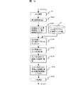
本発明に係る半導体ウェーハの形状計測装置における形状計測のフローを図1に示す。 A flow of shape measurement in the semiconductor wafer shape measurement apparatus according to the present invention is shown in FIG.
先ず、図1(a)に基づいて、SEM装置10を用いたSEM画像の取得方法について説明する。SEM10の電子銃1001から発射された電子線1002を加速電極1003で加速し、集束レンズ1004で収束させ、偏向器1005でX方向及びY方向(図1(a)において図面に垂直な平面内)に走査し、対物レンズ1006で電子線の焦点を計測対象パターンが形成された試料1007の表面に合わせて試料1007の表面を走査して照射する。図1(a)では図示を省略してあるが、試料1007はテーブルに載置されて平面内で移動可能になっており、試料1007の表面の所望の領域が電子線1002の照射領域に位置するように制御される。
First, a method for acquiring an SEM image using the
電子線1002が照射された試料1007の表面から発生した二次電子の一部は検出器1008で検出され、電気信号に変換されて全体制御・画像処理部1009に送られてSEM画像が作成され、演算部1010で記憶部1011に記憶しておいたSEM波形ライブラリの情報を用いSEM画像を処理してパターンの寸法を算出し、結果が出力部1012の画面上に表示される。また、パターン寸法算出結果は、通信回線を介してサーバ1013に記憶される。全体制御・画像処理部1009は、図示していない試料1007を載置するテーブルを含めたSEM10全体の制御も行う。
A part of the secondary electrons generated from the surface of the
演算部1010は、図1(b)に示すように、暫定輪郭抽出部10101、局所投影波形形成分10102、ライブラリマッチング部10103、エッジ位置決定部10104、座標変換・輪郭線抽出部10105、寸法計測部1016を備えている。
As shown in FIG. 1B, the
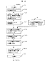
演算部1010における処理手順を図1(c)に示したフローにそってS100〜S600の各ステップを説明する。 The steps of S100 to S600 will be described with reference to the flow shown in FIG.
(S100):SEM10にて取得したSEM画像20から,暫定輪郭抽出部10101において暫定輪郭線を抽出する。暫定的な輪郭線の抽出方法としては,図3に示した従来の技術が適用可能である。以下,図3にて説明する。入力画像105に対して,ノイズを除去するための平滑化処理を施し(601),ソーベルフィルタ等のエッジ強調フィルタ処理によりエッジを検出し(602),二値化処理を行うことによりエッジ部が“1”,エッジ部以外は“0”の二値画像を得る(603)。続いて,パターン幅が1画素になるまで収縮を行う等の細線化処理により中心線を検出する(604)。得られた線画(112)が暫定輪郭線となる。
(S100): The temporary
(S200):本ステップでは,局所投影波形形成分10102において、S100で得られた輪郭線に沿った局所領域にて輪郭線の接線方向に画像を投影し,局所投影波形を生成する。図6にて本ステップを補足する。なお,図6(a)は,図5の部位B付近を拡大したものである。点線112が,S100で抽出される暫定輪郭線である(前述のように,図3に示す方法を用いた場合,暫定輪郭線は概ねホワイトバンドの中心線となる)。暫定輪郭線112にそって,その接線方向の一定長さp1だけ画像を投影する。すなわち,局所矩形領域202,203,204・・・ごとに,矢印の方向に画像を投影することによって,図6(b)に示すような局所投影波形210を得る。投影長p1,及び,投影波形を得るピッチp2は固定値としても良いし,輪郭線の曲率に応じて、曲率が大きい部位ではp1及びp2を小さく,曲率が小さい部位ではp1,p2を大きくというように,パターン形状に応じて可変としても良い。
(S200): In this step, in the local projection
(S300):本ステップでは,ライブラリマッチング部10103において、S200で得られた局所投影波形と,予め作成しておいた,記憶部1011に記憶されているSEM波形ライブラリ30とのマッチングを行う。SEM波形ライブラリ30とは,試料の断面形状とSEM波形を関連づけたもので,例えば,非特許文献2に示されている方法,すなわち,電子線シミュレーション(モンテカルロシミュレーション)にて様々な断面形状におけるSEM波形を計算することによって作成可能である。
(S300): In this step, the
図7はSEM波形ライブラリの概念図である。横軸は試料のテーパ角,縦軸はトップコーナの丸まりの程度であり,モンテカルロシミュレーションによって計算されたパターンの各断面形状701におけるSEM波形702が,断面形状と対になって保存されている。波形マッチングによりライブラリに保存されているSEM波形の中から,S200で得られた局所投影波形と最も良く一致するものを選択することにより,局所投影波形が取得された部位におけるパターンの断面形状が推定されることになる。なお,図7では,簡単のためパターンの断面形状をテーパ角,トップコーナの丸まりの2個のパラメータで表現したが,実際は,計測対象パターンに応じて,その断面形状を表現するのに上記二つのパラメータ以外にも必要なパラメータを持つ必要がある。例えば,パターンの高さ,ボトムコーナの丸まりなどが考えられる。また,パターンの断面形状を表現するためのパラメータ種,各パラメータの変動範囲の決定にあたって,「背景の技術」の項目で述べた光露光シミュレーション結果を利用することも可能である。
FIG. 7 is a conceptual diagram of the SEM waveform library. The horizontal axis indicates the taper angle of the sample, and the vertical axis indicates the degree of rounding of the top corner. The
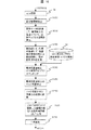
(S400):本ステップでは,エッジ位置決定部10104において、S300で推定されたパターンの断面形状に基づき局所投影波形上のエッジ位置を決定する。SEM波形ライブラリ30上では,パターンの断面形状とその部分のSEM波形の対応関係が既知なので,パターンの断面形状に対して所望のパターンのエッジ端(例えば,ボトム端)を定義することにより,対になっているSEM波形にその位置が伝搬され,さらに,局所投影波形上のどの位置に相当するかが伝搬される。
(S400): In this step, the edge
図8にパターン断面のエッジ端をユーザが指定するためのGUI画面の例を示す。図8(b)のように所定のパーセンテージにおけるエッジ端を検出するか(0%とすればボトム端となる),あるいは,図8(c)のように所定の高さにおけるエッジ端を検出するかを(0nmと指定すればボトム端となる),用途に応じて指定する。 FIG. 8 shows an example of a GUI screen for the user to specify the edge of the pattern cross section. The edge edge at a predetermined percentage is detected as shown in FIG. 8B (or 0% to be the bottom edge), or the edge edge at a predetermined height is detected as shown in FIG. 8C. (Specify 0nm as the bottom edge).
(S500):本ステップでは,座標変換・輪郭線抽出部10105において、S400で決定された局所投影波形上のエッジ位置をSEM画像上の位置に変換する。
(S500): In this step, the coordinate conversion /
(S600):更に座標変換・輪郭線抽出部10105において、S500で求めたSEM画像上の座標の連なりとして,最終的な輪郭線を求める。
(S600): Further, the coordinate transformation /
(S700):寸法計測部10106において、S600で求めた輪郭線を用いてパターンの所望の位置の寸法又は隣接するパターンの間隔を計測する。
(S700): The
S700で計測した結果は、出力部1012の画面上に表示されると共に、通信回線を介してサーバ1013に記憶される。
The result measured in S700 is displayed on the screen of the
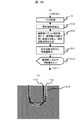
出力部1012の画面上に表示される例として、図6と同じ部位に対応するS600で求めた最終的な輪郭線を表示する場合を図9に示す。図9において,SEM画像901上に重ねて表示されている点線112はS100で求められる暫定輪郭線であり,実線113が最終的な輪郭線である。
As an example displayed on the screen of the
得られた輪郭線113は,例えば,太い実践で示した設計データ114との比較に用いることができる。このように設計データと比較することにより,例えばエッジプレースメントエラー量E,あるいは,設計上の線幅L1と,実際の線幅L2とがどの程度異なっているかといった評価を,従来の技術によって求められる輪郭線112を用いた場合と比べてより高い信頼度を持って行なうことが出来るようになり、より高精度なOPC検証が可能となる。
The obtained
また,本発明は、OPC検証に限らず,プロセス変動のモニタする用途に手適用することも可能である。また,シリコンウェーハ上に転写されたパターンの形状計測に限らず,同様の方法を,フォトマスクの形状計測に対して適用することも可能である。 In addition, the present invention is not limited to OPC verification, and can be manually applied to a use for monitoring process variations. In addition to the shape measurement of the pattern transferred onto the silicon wafer, the same method can be applied to the shape measurement of the photomask.
図10は,本発明の第2の実施の形態に係わる形状計測のフローである。本実施例におけるSEMシステムの構成は、基本的には実施例1で説明した図1に示した構成と同じであるが、演算部1010の構成が多少異なる。
FIG. 10 is a flow of shape measurement according to the second embodiment of the present invention. The configuration of the SEM system in the present embodiment is basically the same as the configuration shown in FIG. 1 described in the first embodiment, but the configuration of the
図10(a)に、本実施例における演算部1020の構成を示す。 演算部1020は、暫定輪郭抽出部10201、局所投影波形形成分10202、特徴量算出部10203、代表点抽出部10204、ライブラリマッチング部10205、エッジ位置決定部10206、座標変換・輪郭線抽出部10207、寸法計測部10208を備えている。
FIG. 10A shows the configuration of the
以下,図10(b)に示したフローにそって各ステップを説明する。 Hereinafter, each step will be described along the flow shown in FIG.
(S110):第1の実施の形態におけるS100と同様に、SEM10で検査対象試料を撮像し全体制御・画像処理部1009から出力されたSEM画像20から,暫定輪郭抽出部10201において暫定輪郭線を抽出する。
(S110): Similar to S100 in the first embodiment, the provisional
(S210):第1の実施の形態におけるS200と同様に、局所投影波形形成分10202において、S100で得られた輪郭線に沿った局所領域にて輪郭線の接線方向に画像を投影し,局所投影波形を生成する。
(S210): Similar to S200 in the first embodiment, in the local projection
(S211):本ステップでは,特徴量算出部10203において、S210で生成した局所投影波形から,図11(a)に示すようなパターン断面形状1100に対して種々の特徴量を算出する。図11(b)において,特徴量f1はホワイトバンド幅である。ホワイトバンド幅は,垂直上方からみた場合のエッジ部の見込み幅を反映する特徴量である。特徴量f2は,ホワイトバンド部において,ピーク位置より外側部の平均幅であり,ボトム部1102の曲率の大きさを反映する特徴量である。特徴量f3は,ホワイトバンド部において,ピーク位置より内側部の平均幅であり,トップ部1101の曲率の大きさを反映する特徴量である。特徴量f4は信号強度の大きさであり,図7が示すようにテーパ角の大きさを反映する特徴量である。
(S211): In this step, the feature
(S212):本ステップでは,代表点抽出部10204において、S211における暫定輪郭線上の各点における特徴量の算出結果に基づき,ライブラリマッチングを行う代表点を決定する。図12(b)は,図11(b)に示した特徴量f1,すなわち,ホワイトバンド幅が図12(a)に示したSEM画像121上における暫定輪郭線122にそってどのように変化しているかを示したものである。ホワイトバンド幅は,図12(a)における始点からポイントP1までほぼ一定,その後ポイントP2まで緩やかに増加,その後ポイントP3まで急激に減少し,P3から終点まではほぼ一定という具合に推移している。特徴量の推移は断面形状の推移の現れといえる。種々の特徴量が一定であれば,概ね断面形状が等しいことを意味しているので,次ステップにおいて全点で断面形状を推定する必要はない。
(S212): In this step, the representative
そこで,本ステップでは,特徴量の推移に基づき,断面形状の推定を行うべき代表点を決定する。図12(b)において,黒丸を付した点が代表点である。同図のように,代表点間隔は,特徴量の変化率が小さい領域では広く,特徴量の変化率が大きい領域では狭くする。図11(b)のように複数の特徴量を用いる場合には,特徴量ごとに代表点間隔を求め,それらの平均値,あるいは,最小代表点間隔を採用するようにする。 Therefore, in this step, a representative point on which the cross-sectional shape should be estimated is determined based on the transition of the feature amount. In FIG. 12B, the points with black circles are representative points. As shown in the figure, the representative point interval is wide in the region where the change rate of the feature amount is small and narrow in the region where the change rate of the feature amount is large. When a plurality of feature amounts are used as shown in FIG. 11B, the representative point interval is obtained for each feature amount, and the average value or the minimum representative point interval is adopted.
(S310):本ステップでは,ライブラリマッチング部10205で、S210で決定した代表点について,予め作成して記憶部1011に記憶しておいた,SEM波形ライブラリ30とのマッチングを行い,断面形状の推定を行う。マッチングの方法は第1の実施の形態のS300で説明した方法と同様である。
(S310): In this step, the
(S410):本ステップでは,エッジ位置決定部10206において、S301で推定された断面形状に基づき局所投影波形上のエッジ位置を決定する。方法は第1の実施の形態のS400で説明した方法と同様である。
(S410): In this step, the edge
(S411):本ステップでは,エッジ位置決定部10206で、各代表点においてS110で算出した暫定輪郭線の局所投影波形上の位置(図13(a)の黒三角点)と,S410で算出したエッジ位置(図13(b)の黒丸点)との距離dを算出する。dの算出結果をプロットした結果を図13(b)上の白丸点として示す。
(S411): In this step, the edge
(S412):本ステップでは,エッジ位置決定部10206で、代表点にて算出した上記dの値(図13(b)の白丸点)を補間することで(図13(b)の破線が補間結果)全点のd値を求め,暫定輪郭線の位置をd値に基づき補正することで,全投影波形上のエッジ位置を決定する。
(S412): In this step, the edge
(S510)第1の実施の形態と同様に、座標変換・輪郭線抽出部10207において、S412で決定された局所投影波形上のエッジ位置をSEM画像上の位置に変換する。
(S510) As in the first embodiment, the coordinate conversion /
(S610)第1の実施の形態と同様に、座標変換・輪郭線抽出部10208において、S510で求めたSEM画像上の座標の連なりとして,最終的な輪郭線を求める。
(S610) As in the first embodiment, the coordinate transformation /
(S710):寸法計測部10208において、S610で求めた輪郭線を用いてパターンの所望の位置の寸法又は隣接するパターンの間隔を計測する。
(S710): The
S710で計測した結果は、出力部1012の画面上に表示されると共に、通信回線を介してサーバ1013に記憶される。
The result measured in S710 is displayed on the screen of the
出力部1012の画面上への表示は、第1の実施例において図9を用いて説明したものと同じである。
The display on the screen of the
第2の実施の形態によれば,演算時間が要するライブラリマッチング処理を代表点についてのみ行うので,より高速な処理が可能である。 According to the second embodiment, library matching processing that requires computation time is performed only for representative points, so higher speed processing is possible.
図14は,本発明の第3の実施の形態に係わる形状計測のフローである。本実施例による形状計測のフローは基本的には図1を用いて説明した第1の実施の形態の場合と同じであるが、第1及び第2の実施の形態においては,局所投影波形から断面形状を推定するのに,記憶部1011に記憶しておいたパターンの断面形状701とSEM波形702を関連づけたライブラリ30を用いたのに対して,本実施の形態においては,パターンの断面形状701’とSEM波形702’から算出した特徴量を関連づけた,SEM波形特徴量ライブラリ31を記憶部1011に記憶させておいて、これを用いるようにした点で異なる。すなわち、図14に示した処理フローの中で、S221とS320とが図1で説明した処理フローと異なる点である。
FIG. 14 is a flow of shape measurement according to the third embodiment of the present invention. The flow of shape measurement according to the present embodiment is basically the same as that of the first embodiment described with reference to FIG. 1, but in the first and second embodiments, the local projection waveform is used. In order to estimate the cross-sectional shape, the
図15(b)にSEM波形特徴量ライブラリ31の概念図を示す。SEM波形特徴量ライブラリ31は,図7に示した電子線シミュレーションによって図15(a)に示すようなSEM波形ライブラリ30を作成した後,得られたSEM波形702’から,図11に示した波形特徴量f1〜f4を算出することによって作成する。図15(a)に示すように,SEM波形特徴量ライブラリ31は,特徴量ごとの,断面形状パラメータ(テーパ角,トップコーナの丸まりなど)に対する特徴量の変化を記述したテーブルである。
FIG. 15B shows a conceptual diagram of the SEM waveform
図14で、SEM波形特徴量ライブラリ31とのマッチングを行うステップ(S320)においては,最尤法を適用するなどして,局所投影波形から算出した特徴量群(f1〜fn)が最も合致する断面形状パラメータの組み合わせ(テーパ角,トップコーナの丸まりなど)を求める。 In FIG. 14, in the step of matching with the SEM waveform feature quantity library 31 (S320), the feature quantity groups (f1 to fn) calculated from the local projection waveforms by applying the maximum likelihood method or the like most closely match. Find the cross-sectional shape parameter combination (taper angle, rounded top corner, etc.).
なお,本実施の形態を,第2の実施の形態と組み合わせることも可能である。 Note that this embodiment can be combined with the second embodiment.
図16は,本発明の第4の実施の形態に係わる形状計測のフローである。
本実施例による形状計測のフローは基本的には図1を用いて説明した第1の実施の形態の場合と同じであるが、異なる点は、本実施の形態においては,暫定輪郭線を抽出(S130)した後,設計データとのマッチングを行い,設計データを参照することで,輪郭線上の各点について,近傍エッジとの距離を算出しておく(S131)点である。
FIG. 16 is a flow of shape measurement according to the fourth embodiment of the present invention.
The flow of shape measurement according to the present embodiment is basically the same as that of the first embodiment described with reference to FIG. 1 except that a temporary contour line is extracted in this embodiment. After (S130), matching with the design data is performed, and by referring to the design data, the distance from the neighboring edge is calculated for each point on the contour line (S131).
図17(a)に設計データのイメージ図を示すが、この図おいて、例えば,着目点111に対しては,近傍に他のエッジが存在しないので「距離大」という情報を付与し,着目点112は近傍エッジが距離wの位置に存在するので「距離w」という情報を付与する。
FIG. 17A shows an image diagram of the design data. In this figure, for example, the point of
局所投影波形を作成するステップ(S230)は第1の実施の形態のS200と同様である。本実施の形態で使用するSEM波形ライブラリ32の概念図を図17(b)に示す。ライブラリを作成する際は,近傍エッジとの距離を変化させて電子線シミュレーションを行いパターンの断面形状701”とSEM波形702”との関係を求め,それら全部の結果をライブラリとして保存する。局所投影波形とSEM波形ライブラリ32とのマッチングを行う際は(S330),S131で付与した近傍エッジとの距離の情報を用い,その距離に相当するライブラリを用いる。
The step of creating a local projection waveform (S230) is the same as S200 of the first embodiment. A conceptual diagram of the
なお,近傍エッジとの距離が設計データ通りになるとは限らないので,マッチングを行う際は(S330),S131で付与された距離情報だけでなく,付与された距離±α[nm]のライブラリとマッチングするようにしても良い。 Since the distance to the neighboring edge is not always the same as the design data, when performing matching (S330), not only the distance information given in S131 but also the given distance ± α [nm] library and You may make it match.
近傍エッジとの距離に応じたSEM波形ライブラリ32を使用するのは,二次電子信号波形が,近傍エッジとの距離によって変化するからである。例えば,エッジ間隔が狭いと、エッジとエッジの間に位置する部位からの二次電子信号強度が小さくなるといった影響を受ける。回路パターンの微細化に伴い,パターン幅,あるいは,パターン間隔が数十nmを下回るようになった場合には,本実施の形態の適用が必要である。
The reason why the
図18は,本発明の第5の実施の形態に係わる形状計測のフローである。
本実施例による形状計測のフローは基本的には図1を用いて説明した第1の実施の形態の場合と同じであるが、異なる点は、本実施の形態においては,暫定輪郭線を抽出(S140)した後,暫定輪郭線に沿った局所領域にて,部分画像を切り出し(S240),三次元の断面形状を対象に電子線シミュレーションを行って作成したSEM像ライブラリ33とのマッチングを行う(S340)点である。S440以降のステップは、基本的に図1で説明したS400以降のステップと同じである。
FIG. 18 is a flow of shape measurement according to the fifth embodiment of the present invention.
The flow of shape measurement according to the present embodiment is basically the same as that of the first embodiment described with reference to FIG. 1 except that a temporary contour line is extracted in this embodiment. After (S140), a partial image is cut out in a local region along the temporary contour line (S240), and matching with the SEM image library 33 created by performing electron beam simulation on the three-dimensional cross-sectional shape is performed. (S340) point. The steps after S440 are basically the same as the steps after S400 described in FIG.
本実施の形態は,ホールパターン,ラインエンドなど、直線的なパターンエッジが存在しない部位において有効である。第4の実施の形態と同じように,設計データを参照して,部位ごとに,局所投影波形を用いるか,部分画像を用いるかを切り替えるようにしても良い。 This embodiment is effective in a portion where there is no linear pattern edge, such as a hole pattern or a line end. As in the fourth embodiment, the design data may be referred to switch between using a local projection waveform or a partial image for each part.
図19(a)は,本発明の第6の実施の形態に係わる形状計測のフローである。ステップS150,S250,S251までは,第2の実施の形態のステップS110,S210及びS211と同様である。第2の実施の形態においては,S210で算出した波形特徴量を代表点の三択に用いているが,本実施の形態は、S251で算出した波形特徴量の算出結果をユーザに提示して(S252)終了する。 FIG. 19A shows a flow of shape measurement according to the sixth embodiment of the present invention. Steps S150, S250, and S251 are the same as steps S110, S210, and S211 of the second embodiment. In the second embodiment, the waveform feature value calculated in S210 is used for the three choices of representative points. However, in this embodiment, the calculation result of the waveform feature value calculated in S251 is presented to the user. (S252) The process ends.
図19(b)は,波形特徴量の表示画面の例である(部位は図9と同じ)。同図は,S150で抽出した暫定輪郭線112にそって生成した局所投影波形から算出した特徴量f1(ホワイトバンド幅)を,その値に応じて,色分けして表示したものである。
FIG. 19B is an example of a waveform feature amount display screen (the parts are the same as those in FIG. 9). The figure shows the feature value f1 (white band width) calculated from the local projection waveform generated along the
前述のように,波形特徴量は試料の断面形状を反映しているので,部位によって断面形状がどう変化しているかを捉える用途に有効である。また,色分け表示の基となっているデータは,図12の下段に示したデータであるが,このデータを蓄積し,プロセスモニタに活用することも可能である。 As described above, since the waveform feature value reflects the cross-sectional shape of the sample, it is effective for the purpose of capturing how the cross-sectional shape changes depending on the part. The data that is the basis of the color-coded display is the data shown in the lower part of FIG. 12, but this data can be stored and used for process monitoring.
第1〜第5の実施の形態においては,単一の輪郭線を出力したが,例えば,SEM画像2000上で高さ0%(2001),25%(2002),50%(2003),75%(2004)といった具合に,複数のエッジ端を出力するようにしても良い(図20参照)。あるいは,各点における断面形状が推定済みなので,等高線として出力しても良い。
In the first to fifth embodiments, a single contour line is output. For example, the height is 0% (2001), 25% (2002), 50% (2003), 75 on the
レジストパターンにおいては,所謂,膜減り(レジスト高さの減少)の状況把握が重要であるため,特に,出力結果を比較する対象として,「背景技術」の項目で述べた,光露光シミュレーション結果と比較する場合には,本実施の形態が有効である。 In resist patterns, it is important to understand the situation of so-called film reduction (resist height reduction). In particular, the results of light exposure simulations described in the section of “Background Technology” are used as targets for comparing output results. In the case of comparison, this embodiment is effective.
10・・・電子顕微鏡 20・・・SEM画像 30〜33・・・ライブラリ 112・・・暫定輪郭線 113・・・最終出力の輪郭線 114・・・設計データ 202〜20・・・局所矩形領域 210・・・局所投影波形 212・・・色分け表示した波形特徴量 S100〜S700・・・形状計測のステップ
DESCRIPTION OF
Claims (14)
前記試料のパターンの断面形状と該パターンの断面形状に対応する電子線信号波形情報とを関連づけるライブラリを記憶する記憶手段と、
該電子線画像取得手段で取得した前記試料のパターンの画像から得られる情報を前記記憶手段に記憶されたライブラリ情報を参照して処理することにより前記パターンの寸法情報を抽出する寸法情報抽出手段と、
該寸法情報抽出手段で抽出した前記パターンの寸法に関連する情報を画面上に表示する出力手段と
を備えた電子顕微鏡システム。 An electron beam image acquisition means for acquiring an image of a desired portion of a sample having a pattern formed on the surface using a scanning electron microscope;
Storage means for storing a library associating the cross-sectional shape of the pattern of the sample with the electron beam signal waveform information corresponding to the cross-sectional shape of the pattern;
Dimension information extraction means for extracting dimension information of the pattern by processing information obtained from the image of the pattern of the sample acquired by the electron beam image acquisition means with reference to library information stored in the storage means; ,
An electron microscope system comprising: output means for displaying information related to the dimension of the pattern extracted by the dimension information extracting means on a screen.
前記試料のパターンの断面形状と該パターンの断面形状に対応する電子線信号波形情報とを関連づけるライブラリを記憶し、
前記取得した試料のパターンの画像から得られる情報を前記記憶手段に記憶されたライブラリ情報を参照して処理することにより前記パターンの寸法情報を抽出し、
該抽出した前記パターンの寸法に関連する情報を画面上に表示することを特徴とする電子顕微鏡システムを用いたパターン寸法計測方法。 Obtain an image of the desired part of the sample with a pattern formed on the surface using a scanning electron microscope,
Storing a library associating the cross-sectional shape of the pattern of the sample with the electron beam signal waveform information corresponding to the cross-sectional shape of the pattern;
Extracting the pattern dimension information by processing the information obtained from the acquired pattern image of the sample with reference to the library information stored in the storage means,
A pattern dimension measuring method using an electron microscope system, wherein information relating to the extracted dimension of the pattern is displayed on a screen.
Priority Applications (1)
| Application Number | Priority Date | Filing Date | Title |
|---|---|---|---|
| JP2013144124A JP2013200319A (en) | 2013-07-10 | 2013-07-10 | Electron microscope system and pattern dimension measuring method using the same |
Applications Claiming Priority (1)
| Application Number | Priority Date | Filing Date | Title |
|---|---|---|---|
| JP2013144124A JP2013200319A (en) | 2013-07-10 | 2013-07-10 | Electron microscope system and pattern dimension measuring method using the same |
Related Parent Applications (1)
| Application Number | Title | Priority Date | Filing Date |
|---|---|---|---|
| JP2008040816A Division JP5319931B2 (en) | 2008-02-22 | 2008-02-22 | Electron microscope system and pattern dimension measuring method using the same |
Publications (1)
| Publication Number | Publication Date |
|---|---|
| JP2013200319A true JP2013200319A (en) | 2013-10-03 |
Family
ID=49520646
Family Applications (1)
| Application Number | Title | Priority Date | Filing Date |
|---|---|---|---|
| JP2013144124A Pending JP2013200319A (en) | 2013-07-10 | 2013-07-10 | Electron microscope system and pattern dimension measuring method using the same |
Country Status (1)
| Country | Link |
|---|---|
| JP (1) | JP2013200319A (en) |
Cited By (3)
| Publication number | Priority date | Publication date | Assignee | Title |
|---|---|---|---|---|
| JP2017067542A (en) * | 2015-09-29 | 2017-04-06 | 株式会社 ベセル | Inspection method and specimen device in immunochromatography |
| JP2018152217A (en) * | 2017-03-13 | 2018-09-27 | 株式会社日立製作所 | Charged particle beam device |
| CN117115194A (en) * | 2023-10-20 | 2023-11-24 | 华芯程(杭州)科技有限公司 | Contour extraction method, device, equipment and medium based on electron microscope image |
Citations (7)
| Publication number | Priority date | Publication date | Assignee | Title |
|---|---|---|---|---|
| JPS622116A (en) * | 1985-06-28 | 1987-01-08 | Nec Corp | Measurement of shape |
| JPS63266747A (en) * | 1987-04-24 | 1988-11-02 | Nikon Corp | Sample image display device |
| JP2004219343A (en) * | 2003-01-17 | 2004-08-05 | Hitachi High-Technologies Corp | Method of measuring three-dimensional profile of detailed pattern |
| JP2005156436A (en) * | 2003-11-27 | 2005-06-16 | Hitachi Ltd | Semiconductor pattern measuring method and process control method |
| JP2005189137A (en) * | 2003-12-26 | 2005-07-14 | Hitachi High-Technologies Corp | Pattern measuring method |
| JP2007120968A (en) * | 2005-10-25 | 2007-05-17 | Hitachi High-Technologies Corp | Electron beam type dimension measuring device, and dimension measuring method using it |
| JP2007218711A (en) * | 2006-02-16 | 2007-08-30 | Hitachi High-Technologies Corp | Method for measuring measurement target pattern using electron microscope device |
-
2013
- 2013-07-10 JP JP2013144124A patent/JP2013200319A/en active Pending
Patent Citations (7)
| Publication number | Priority date | Publication date | Assignee | Title |
|---|---|---|---|---|
| JPS622116A (en) * | 1985-06-28 | 1987-01-08 | Nec Corp | Measurement of shape |
| JPS63266747A (en) * | 1987-04-24 | 1988-11-02 | Nikon Corp | Sample image display device |
| JP2004219343A (en) * | 2003-01-17 | 2004-08-05 | Hitachi High-Technologies Corp | Method of measuring three-dimensional profile of detailed pattern |
| JP2005156436A (en) * | 2003-11-27 | 2005-06-16 | Hitachi Ltd | Semiconductor pattern measuring method and process control method |
| JP2005189137A (en) * | 2003-12-26 | 2005-07-14 | Hitachi High-Technologies Corp | Pattern measuring method |
| JP2007120968A (en) * | 2005-10-25 | 2007-05-17 | Hitachi High-Technologies Corp | Electron beam type dimension measuring device, and dimension measuring method using it |
| JP2007218711A (en) * | 2006-02-16 | 2007-08-30 | Hitachi High-Technologies Corp | Method for measuring measurement target pattern using electron microscope device |
Cited By (4)
| Publication number | Priority date | Publication date | Assignee | Title |
|---|---|---|---|---|
| JP2017067542A (en) * | 2015-09-29 | 2017-04-06 | 株式会社 ベセル | Inspection method and specimen device in immunochromatography |
| JP2018152217A (en) * | 2017-03-13 | 2018-09-27 | 株式会社日立製作所 | Charged particle beam device |
| CN117115194A (en) * | 2023-10-20 | 2023-11-24 | 华芯程(杭州)科技有限公司 | Contour extraction method, device, equipment and medium based on electron microscope image |
| CN117115194B (en) * | 2023-10-20 | 2024-01-30 | 华芯程(杭州)科技有限公司 | Contour extraction method, device, equipment and medium based on electron microscope image |
Similar Documents
| Publication | Publication Date | Title |
|---|---|---|
| JP5319931B2 (en) | Electron microscope system and pattern dimension measuring method using the same | |
| US10223784B2 (en) | Pattern evaluation device and visual inspection device comprising pattern evaluation device | |
| US20160035538A1 (en) | Pattern Shape Evaluation Method, Semiconductor Device Manufacturing Method, and Pattern Shape Evaluation Device | |
| JP6043735B2 (en) | Image evaluation apparatus and pattern shape evaluation apparatus | |
| JP5433522B2 (en) | Pattern dimension measuring method using electron microscope, pattern dimension measuring system, and method for monitoring change with time of electron microscope apparatus | |
| JP2005156436A (en) | Semiconductor pattern measuring method and process control method | |
| JP4512395B2 (en) | Exposure process monitoring method and apparatus | |
| JP2009222454A (en) | Pattern measuring method and device | |
| TWI698705B (en) | Pattern measuring method and pattern measuring device | |
| JP5966087B2 (en) | Pattern shape evaluation apparatus and method | |
| JP6147868B2 (en) | Pattern measuring apparatus and computer program | |
| JP2013200319A (en) | Electron microscope system and pattern dimension measuring method using the same | |
| JP5880134B2 (en) | Pattern measuring method and pattern measuring apparatus | |
| JP6018803B2 (en) | Measuring method, image processing apparatus, and charged particle beam apparatus | |
| JP2017102039A (en) | Pattern measurement program, pattern measurement method, and device | |
| JP6581835B2 (en) | Semiconductor device evaluation condition setting method and evaluation condition setting apparatus | |
| JP2016217816A (en) | Pattern measurement device, pattern measurement method, and pattern measurement program | |
| JP5389840B2 (en) | Pattern shape evaluation method and pattern shape evaluation apparatus | |
| JP2013164356A (en) | Charged particle beam device, and operation condition setting device of charged particle beam device | |
| JP2014182117A (en) | Electron microscope system and pattern measuring method using the same | |
| JP6294099B2 (en) | Pattern measuring apparatus and pattern measuring apparatus management apparatus | |
| JP5695716B2 (en) | Pattern dimension calculation method and image analysis apparatus | |
| JP2010236978A (en) | Method of calculating pattern dimension, and method and device for analyzing image |
Legal Events
| Date | Code | Title | Description |
|---|---|---|---|
| A521 | Written amendment |
Free format text: JAPANESE INTERMEDIATE CODE: A523 Effective date: 20130710 |
|
| A621 | Written request for application examination |
Free format text: JAPANESE INTERMEDIATE CODE: A621 Effective date: 20130710 |
|
| A521 | Written amendment |
Free format text: JAPANESE INTERMEDIATE CODE: A523 Effective date: 20130710 |
|
| A977 | Report on retrieval |
Free format text: JAPANESE INTERMEDIATE CODE: A971007 Effective date: 20140221 |
|
| A131 | Notification of reasons for refusal |
Free format text: JAPANESE INTERMEDIATE CODE: A131 Effective date: 20140325 |
|
| A02 | Decision of refusal |
Free format text: JAPANESE INTERMEDIATE CODE: A02 Effective date: 20140715 |