JP2013168894A - Antenna device and communication terminal having the same - Google Patents
Antenna device and communication terminal having the same Download PDFInfo
- Publication number
- JP2013168894A JP2013168894A JP2012032253A JP2012032253A JP2013168894A JP 2013168894 A JP2013168894 A JP 2013168894A JP 2012032253 A JP2012032253 A JP 2012032253A JP 2012032253 A JP2012032253 A JP 2012032253A JP 2013168894 A JP2013168894 A JP 2013168894A
- Authority
- JP
- Japan
- Prior art keywords
- antenna
- slit
- frequency band
- communication
- antenna device
- Prior art date
- Legal status (The legal status is an assumption and is not a legal conclusion. Google has not performed a legal analysis and makes no representation as to the accuracy of the status listed.)
- Pending
Links
Images


Landscapes
- Variable-Direction Aerials And Aerial Arrays (AREA)
Abstract
Description
本発明は、相手側機器と電磁界信号を介して通信する短距離無線通信システムに用いられるアンテナ装置及びそれを備えた通信端末に関するものである。 The present invention relates to an antenna device used in a short-range wireless communication system that communicates with a counterpart device via an electromagnetic field signal, and a communication terminal including the antenna device.
近年、携帯通信機器、例えば携帯電話機は小型化が進んでいる。このため、携帯電話機に用いられる通話用アンテナも小型化する必要があるが、小型化による特性劣化が問題となる。そこで、携帯電話機の筐体の金属部分等を放射素子として作用させるものがある。この場合、通話用アンテナ単体の場合よりも良好な特性を得ることが可能となる。 In recent years, mobile communication devices such as mobile phones have been downsized. For this reason, it is necessary to reduce the size of a call antenna used in a mobile phone, but there is a problem of characteristic deterioration due to the size reduction. Therefore, there is one in which a metal portion or the like of a casing of a mobile phone acts as a radiating element. In this case, it is possible to obtain better characteristics than in the case of a telephone antenna alone.
また、近年の携帯電話機等にはNFC(Near Field Communication)システムが搭載されていることが多い。NFCシステムでは、携帯電話機同士又は携帯電話機とリーダ/ライタ装置とで通信を行うために、各々の機器に通信用のコイルアンテナ等のアンテナを設ける必要がある。しかしながら、前記のように小型化された携帯電話機等の筺体内にはNFC用のアンテナを設置するための十分なスペースを設けることが難しい場合がある。 In recent years, NFC (Near Field Communication) systems are often installed in mobile phones and the like. In the NFC system, in order to perform communication between mobile phones or between a mobile phone and a reader / writer device, it is necessary to provide each device with an antenna such as a coil antenna for communication. However, in some cases, it is difficult to provide a sufficient space for installing an NFC antenna in a housing of a mobile phone or the like downsized as described above.
そこで、例えば特許文献1に開示されているように、NFC用ICチップに小型のコイル導体を接続し、このコイル導体に隣接配置した大面積の導体層から無線信号を送信する、といった構成がとられることがある。特許文献1に記載のアンテナ装置は、スリット及び開口部が形成された導体層と、平面視でコイル開口部が導体層の開口部と重なるよう配置されたコイル導体とを備えている。そして、コイル導体に電流が流れて発生する磁束が導体層の開口部を通るため、導体層の開口部にはコイル導体に流れる電流とは反対方向に電流が流れ、その電流は縁端効果によりスリットを介して導体層の縁端に沿って流れる。これにより、導体層はコイル導体の磁界を強める所謂ブースターアンテナとして機能する。この構成によれば、導体層は薄い金属膜でもよいため、例えばプリント配線板と端末筺体とのわずかな隙間に導体層を設けることができる。 Therefore, for example, as disclosed in Patent Document 1, a small coil conductor is connected to an NFC IC chip, and a radio signal is transmitted from a large-area conductor layer disposed adjacent to the coil conductor. May be. The antenna device described in Patent Literature 1 includes a conductor layer in which a slit and an opening are formed, and a coil conductor that is arranged so that the coil opening overlaps with the opening of the conductor layer in plan view. Since the magnetic flux generated by the current flowing through the coil conductor passes through the opening of the conductor layer, the current flows in the direction opposite to the current flowing through the coil conductor through the opening of the conductor layer. It flows along the edge of the conductor layer through the slit. Thus, the conductor layer functions as a so-called booster antenna that strengthens the magnetic field of the coil conductor. According to this configuration, since the conductor layer may be a thin metal film, for example, the conductor layer can be provided in a slight gap between the printed wiring board and the terminal casing.
携帯電話機にNFC等のHF帯用のアンテナを設けた場合、例えば、GSM(登録商標)又はCDMA等の通話用アンテナ、又は所謂ワンセグ等の地上デジタル放送用アンテナ等のUHF帯の電界結合型アンテナの放射板、及びHF帯のアンテナのブースターアンテナとして同じ平面導体(グランド導体)を用いることで、部品点数の増加を抑制し、配置スペースの削減、又はコストダウンを実現できる。小型化された携帯電話機内ではUHF帯のアンテナ等、HF帯とは異なる周波数帯を有するアンテナとHF帯のアンテナとが互いに干渉するといった問題がある。具体的には、UHF帯アンテナによって発生する電流が平面導体(グランド電極)に流れる際に、その電流がUHF帯のアンテナのコイル導体に貼りつけた磁性体シート付近を流れると、磁性体シートによる損失により通話用アンテナの通信特性が劣化するおそれがある。 When a mobile phone is provided with an antenna for HF band such as NFC, for example, an antenna for telephone call such as GSM (registered trademark) or CDMA, or an electric field coupling type antenna for UHF band such as a so-called terrestrial digital broadcasting antenna such as One Seg By using the same planar conductor (ground conductor) as the radiating plate and the booster antenna of the HF band antenna, it is possible to suppress an increase in the number of parts and to reduce the arrangement space or reduce the cost. In a miniaturized mobile phone, there is a problem that an antenna having a frequency band different from the HF band and an antenna in the HF band interfere with each other, such as an antenna in the UHF band. Specifically, when the current generated by the UHF band antenna flows through the planar conductor (ground electrode), if the current flows near the magnetic sheet attached to the coil conductor of the UHF band antenna, the magnetic sheet There is a possibility that the communication characteristics of the communication antenna may deteriorate due to the loss.
そこで、本発明の目的は、異なる周波数帯を有するアンテナ同士の干渉を防止するアンテナ装置及びそれを備えた通信端末を提供することにある。 Therefore, an object of the present invention is to provide an antenna device that prevents interference between antennas having different frequency bands, and a communication terminal including the antenna device.
本発明に係るアンテナ装置は、厚み方向に貫通している開口部及び一端部から前記開口部まで延びているスリットが形成された平面導体と、第1周波数帯で動作し、前記平面導体を放射板として用いる電界放射型アンテナと、磁性体層及び前記磁性体層に沿って形成されたコイル導体を有し、前記厚み方向から視て前記開口部と一部が重なる位置に配置され、前記第1周波数帯よりも低い周波数帯である第2周波数帯で動作する磁界結合型アンテナと、前記スリットにより分断された前記平面導体の一部を電気的に接続する接続手段と、を備え、前記接続手段は、前記第1周波数帯に対して実質的に短絡となり、前記第2周波数帯に対して実質的に開放となる、ことを特徴とする。 An antenna device according to the present invention operates in a first frequency band and has an opening that penetrates in the thickness direction and a slit that extends from one end to the opening, and radiates the planar conductor. A field emission antenna used as a plate, a magnetic layer, and a coil conductor formed along the magnetic layer, and disposed at a position partially overlapping the opening as viewed from the thickness direction; A magnetic field coupled antenna that operates in a second frequency band that is a frequency band lower than one frequency band; and a connection means that electrically connects a part of the planar conductor divided by the slit, the connection The means is substantially short-circuited with respect to the first frequency band and substantially open with respect to the second frequency band.
この構成では、電界放射型アンテナ又は磁界結合型アンテナによる何れの通信でも、平面導体を放射素子として用いている。平面導体にはスリットにより分断されていて、接続手段により電気的に接続されている。この接続手段は第1周波数帯に対してローインピーダンスとなり実質的に短絡となる。また、第2周波数帯に対してハイインピーダンスとなり、実質的に開放となる。従って、磁界結合型アンテナによる通信の場合、接続手段は実質的に開放となるため、電流はスリット及び開口部に沿って流れる。電界放射型アンテナによる通信の場合、接続手段は実質的に短絡となるため、電流は接続手段を介して流れることからスリット等に沿って流れることはない。このため、電界放射型アンテナによる通信時に流れる電流が磁界放射型アンテナの磁性体層付近を流れることがなく、磁性体層での損失により電界放射型アンテナによる通信特性が劣化するのを防止できる。 In this configuration, a planar conductor is used as a radiating element in any communication using a field emission antenna or a magnetic field coupling antenna. The planar conductor is divided by a slit and electrically connected by a connecting means. This connection means has a low impedance with respect to the first frequency band and is substantially short-circuited. Moreover, it becomes a high impedance with respect to a 2nd frequency band, and becomes substantially open | released. Therefore, in the case of communication using a magnetic field coupling antenna, the connection means is substantially opened, so that current flows along the slit and the opening. In the case of communication using a field emission antenna, the connection means is substantially short-circuited, so that current does not flow along the slit or the like because it flows through the connection means. For this reason, the current flowing during communication by the field radiation antenna does not flow near the magnetic layer of the magnetic field radiation antenna, and it is possible to prevent the communication characteristics of the field radiation antenna from deteriorating due to loss in the magnetic layer.
前記接続手段は、前記第1周波数帯に対して誘導性を有し、前記第2周波数帯に対して容量性を有するリアクタンス素子であってもよい。 The connecting means may be a reactance element having inductivity with respect to the first frequency band and capacitive with respect to the second frequency band.
前記接続手段は前記平面導体の前記スリットの前記一端部近傍に形成されている構成が好ましい。 The connection means is preferably formed in the vicinity of the one end of the slit of the planar conductor.
この構成では、電界放射型アンテナによる通信の場合に実質的に短絡した接続手段を介して流れる電流が磁性体層からより離れるため、磁性体層の影響をより軽減できる。 In this configuration, since the current flowing through the connection means that is substantially short-circuited in the case of communication using the field emission antenna is further away from the magnetic layer, the influence of the magnetic layer can be further reduced.
アンテナ装置は、前記電界放射型アンテナが配置された基板を備え、前記金属部材の少なくとも一部は前記基板に形成された導体パターンであってもよい。 The antenna device may include a substrate on which the field emission antenna is disposed, and at least a part of the metal member may be a conductor pattern formed on the substrate.
この構成では、平面導体を設けるスペースを別途確保する必要が無くなる。 In this configuration, it is not necessary to separately secure a space for providing the planar conductor.
アンテナ装置は、前記電界放射型アンテナが配置された基板を備え、前記基板の厚み方向で前記導体パターンに対向するよう前記基板に形成され、前記スリットと一部が対向している別の平面導体を備え、前記接続手段は、前記平面導体及び前記別の平面導体間に形成される浮遊容量であってもよい。 The antenna device includes a substrate on which the field emission antenna is disposed, and is formed on the substrate so as to face the conductor pattern in a thickness direction of the substrate, and is another planar conductor partially facing the slit. The connecting means may be a stray capacitance formed between the planar conductor and the another planar conductor.
この構成では、平面導体と他の平面導体との間に形成される浮遊容量を接続手段として用いるため、部品としての容量素子が必要なくなり、省スペース化及びコストダウンを図ることができる。 In this configuration, since the stray capacitance formed between the planar conductor and the other planar conductor is used as the connecting means, a capacitive element as a component is not necessary, and space saving and cost reduction can be achieved.
本発明によれば、電界放射型アンテナによる通信時に流れる電流が磁界結合型アンテナの磁性体層付近を流れないようにでき、その結果、磁性体層での損失により電界放射型アンテナによる通信特性が劣化するのを防止できる。 According to the present invention, it is possible to prevent the current flowing during communication by the field emission antenna from flowing near the magnetic layer of the magnetic coupling type antenna, and as a result, the communication characteristics of the field emission antenna can be reduced by the loss in the magnetic layer. Deterioration can be prevented.
以下に説明する実施形態では、本発明に係る通信端末を携帯電話機とし、本発明に係るアンテナ装置を携帯電話機に搭載した場合について説明する。実施形態に係る携帯電話機は、UHF帯を利用した通話又は電子メール通信等(以下、UHF帯による通信という。)及びNFC等のHF帯による通信(以下、HF帯による通信という。)を行う機能を備えている。 In the embodiments described below, a case will be described in which the communication terminal according to the present invention is a mobile phone and the antenna device according to the present invention is mounted on a mobile phone. The cellular phone according to the embodiment has a function of performing communication using the UHF band, e-mail communication or the like (hereinafter referred to as communication using the UHF band) and communication using an HF band such as NFC (hereinafter referred to as communication using the HF band). It has.
(実施形態1)
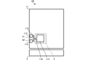
図1は実施形態1に係る携帯電話機が備えるアンテナ装置の模式図である。アンテナ装置1は基板(プリント基板)10を備えている。基板10にはグランド導体パターン(本発明の平面導体)11が形成されている。グランド導体パターン11は基板10の内層に形成されていてもよいし、基板10の最外層(表面)に形成されていてもよい。なお、図1では、グランド導体パターン11以外の基板10の層を破線で示しており、グランド導体パターン11は基板10の内層に形成されている構成を示す。
(Embodiment 1)
FIG. 1 is a schematic diagram of an antenna device provided in the mobile phone according to the first embodiment. The antenna device 1 includes a substrate (printed substrate) 10. A ground conductor pattern (planar conductor of the present invention) 11 is formed on the
グランド導体パターン11は長辺及び短辺からなる矩形状であり、周縁に沿った全長が約3λ/4に設定されている。λは後述の電界放射型アンテナ3によるUHF帯による通信で扱われる通信周波数である。グランド導体パターン11には、長辺側の一端から短辺に沿った方向(以下、短手方向と言う。)に延びたスリット111と、スリット111に連結された矩形状の開口部112とが形成されている。スリット111及び開口部112は基板10の厚み方向にグランド導体パターン11を貫通している。
The
アンテナ装置1はチップコンデンサ(本発明の接続手段)4を備えている。チップコンデンサ4は、グランド導体パターン11の端部近傍にスリット111を跨いで設けられている。チップコンデンサ4は、例えば基板10の表面に設けられ、スルーホール導体等の層間接続導体によりグランド導体パターン11に接続されている。本実施形態に係るアンテナ装置1は、後述するコイルアンテナ(本発明の磁界結合型アンテナ)2及び電界放射型アンテナ3を備えている。コイルアンテナ2又は電界放射型アンテナ3で通信が行われる場合には、縁端効果によりグランド導体パターン11の周縁部に沿って電流が流れる。チップコンデンサ4は、流れる電流に係る周波数に応じてハイインピーダンス又はローインピーダンスとなる。すなわち、グランド導体パターン11のスリット111が形成された部分は、チップコンデンサ4がハイインピーダンスのときには実質的に開放となり、ローインピーダンスのときには実質的に短絡される。本実施形態に係るチップコンデンサ4は30MHz〜300MHz帯の間に自己共振周波数を有し、キャパシタンスが例えば約1000[pF]を有するリアクタンス素子である。
The antenna device 1 includes a chip capacitor (connecting means of the present invention) 4. The
図2(A)はチップコンデンサ4の等価回路を示す図であり、図2(B)はチップコンデンサ4の周波数特性を示す図である。図2(B)では横軸を周波数[MHz]、縦軸をインピーダンス[Ω]としている。チップコンデンサ4の自己共振周波数は、図2(B)に示すように、約200MHzである。チップコンデンサ4は、抵抗R1及びキャパシタC1が並列接続され、さらに、抵抗R2及びインダクタL1が直列接続された構成である。チップコンデンサ4は、自己共振周波数約200MHzより低周波数帯では容量性となり、自己共振周波数より高周波数帯では誘導性となる。
FIG. 2A is a diagram showing an equivalent circuit of the
本実施形態に係るコイルアンテナ2によるHF帯による通信の周波数は約13.56MHz帯(本発明の第2周波数帯)で、電界放射型アンテナ3によるUHF帯による通信の周波数は約400MHz〜2.7GHz帯(本発明の第1周波数帯)である。コイルアンテナ2によってHF帯による通信が行われる場合、チップコンデンサ4はハイインピーダンス(例えば約100Ω)となる。電界放射型アンテナ3によるUHF帯による通信が行われる場合、チップコンデンサ4はローインピーダンス(例えば約1Ω)となる。
The frequency of communication in the HF band by the
アンテナ装置1はNFC通信用のコイルアンテナ2を備えている。コイルアンテナ2はコイル導体21と矩形板状のフレキシブル基板22と矩形板状の磁性体シート23とを備えている。フレキシブル基板22には巻回中心部をコイル開口部CWとする渦巻き状のコイル導体21が形成されている。図1のコイルアンテナ2は分解斜視図として示している。磁性体シート23は例えばシート状に成形したフェライトである。磁性体シート23は、主として、コイルアンテナ2から生じる磁界が、携帯電話機が備える他の電子部品からの影響を受けないためのシールドとして機能している。なお、コイル導体21の巻回数(ターン数)は必要なインダクタンスによって定める。ワンターンであれば単にループ状のコイル導体となる。
The antenna device 1 includes a
コイルアンテナ2は、基板10の厚み方向から視て、コイル開口部CWの一部又は全部がグランド導体パターン11の開口部112と重なる位置に配置されている。また、コイルアンテナ2は、磁性体シート23と基板10との間にフレキシブル基板22が挟まれるよう設けられている。コイルアンテナ2はフレキシブル基板22に形成された接続部(不図示)により、例えば基板10に配置された給電回路(不図示)に接続されている。アンテナ装置1を備える携帯電話機がNFCによる通信を行う場合、給電回路による給電又は通信先から放射された磁界によりコイル導体21及びグランド導体パターン11、スリット111、開口部112の周縁に電流が流れる。
The
なお、基板10にはコイルアンテナ2に対して並列接続されるキャパシタ(不図示)が設けられている。コイルアンテナ2のコイル導体21及び磁性体シート23によって定まるインダクタンスとキャパシタのキャパシタンスとによって共振周波数が定められる。例えばNFCによる通信において中心周波数13.56MHzのHF帯を利用する場合には、共振周波数を13.56MHzに定める。
The
図3は、コイルアンテナ2の通信時にコイルアンテナ2のコイル導体21及びグランド導体パターン11に流れる電流の経路の例を示す図である。図3の破線矢印はコイル導体21に流れる電流の向きを示し、実線矢印はグランド導体パターン11に流れる電流の向きを示す。
FIG. 3 is a diagram illustrating an example of a path of current flowing through the
コイルアンテナ2から磁界を放射する場合、給電回路によりコイル導体21に図中破線矢印方向に電流が流れ、コイル開口部CWから紙面奥方向への磁束が発生する。発生した磁束がグランド導体パターン11の開口部112を通ることで、開口部112の周縁部に沿ってコイル導体21と反対方向に電流が流れる。本実施形態では、コイルアンテナ2は13.56MHz帯で通信を行うため、上述したように、チップコンデンサ4はハイインピーダンスとなり、スリット111部分は実質的に開放となる。よって、発生した電流は、図中実線矢印に示すようにスリット111に沿って流れ、さらに、グランド導体パターン11の周縁に沿って流れる。これにより、グランド導体パターン11から強い磁界が生じ、グランド導体パターン11はコイル導体の磁界を増幅するアンテナ、所謂ブースターアンテナとして機能し、HF帯による通信距離をコイルアンテナ2単体の時と比較してさらに広げることができる。通信相手から放射された磁界を受ける場合には、前記とは逆の動作となる。
When a magnetic field is radiated from the
コイルアンテナ2はコイル開口部CWの一部又は全部が開口部112と重なるように配置されているが、コイル開口部CWと開口部112とがほぼ同じ大きさとし、コイル開口部CWの全部が開口部112と重なるようにした場合、基板10の厚み方向においてコイル導体21が開口部112の周縁と略一致して配置されることになる。このため、コイルアンテナ2のコイル導体21及び開口部112の周縁の結合が強くなり、グランド導体パターン11は、ブースターアンテナとしてより効率よく磁界を放射させることができる。
The
アンテナ装置1は電界放射型アンテナ(本発明の電界放射型アンテナ)3を備えている。電界放射型アンテナ3は略λ/4で共振する放射素子として作用し、グランド導体パターン11は略3λ/4で共振する放射素子として作用するよう形成されている。そして、電界放射型アンテナ3及びグランド導体パターン11でダイポールアンテナを形成している。
The antenna device 1 includes a field radiation antenna (field radiation antenna of the present invention) 3. The
図4は、電界放射型アンテナ3の通信時にグランド導体パターン11に流れる電流の経路の例を示す図である。電界放射型アンテナ3及びグランド導体パターン11には給電部5が接続されている。給電部5から電界放射型アンテナ3及びグランド導体パターン11に電流が流れることにより、電界放射型アンテナ3及びグランド導体パターン11は携帯電話機のUHF帯による通信用のアンテナ(ダイポールアンテナ)として機能する。UHF帯の通信周波数は400MHz〜2.7GHz帯であるため、上述したように、チップコンデンサ4はローインピーダンスとなる。よって、スリット111部分は実質的に短絡となり、給電部5からの電流は、チップコンデンサ4を介してスリット111を横切り、グランド導体パターン11の周縁に沿って流れる。
FIG. 4 is a diagram illustrating an example of a path of a current flowing through the
もし、UHF帯による通信時に給電部5から流れる電流がスリット111及び開口部112に沿って流れると、スリット111及び開口部112に沿って流れる電流は、磁性体シート23近傍を流れることになる。磁性体シート23(図1参照)は400MHz〜2.7GHz等の高周波数帯において損失が大きいため、磁性体シート23近傍を電流が流れると磁性体シート23の影響を受ける。
If the current flowing from the power feeding unit 5 flows along the
本実施形態では、UHF帯による通信が行われる場合にはチップコンデンサ4がローインピーダンスとなるため、給電部5から流れる電流がスリット111及び開口部112に沿って流れることはない。従って、データ通信の共振点がずれることがないため、UHF帯による通信の通信特性の劣化を抑制できる。
In the present embodiment, since the
このように、本実施形態では、通信特性を劣化させることなく、共通のグランド導体パターン11をHF帯による通信及びUHF帯による通信の二つの通信で放射素子として用いることができる。このため、アンテナ装置1の部品点数を削減でき、コストダウンを図れる。また、UHF帯による通信においてスリット111及び開口部112に沿って電流が流れる場合、スリット111等の長さを考慮してグランド導体パターン11を設計する必要があるが、チップコンデンサ4によりスリット111部分を短絡させることで、UHF帯による通信におけるスリット111等の長さを無視でき、設計の手間を省くことができる。
As described above, in this embodiment, the common
なお、本実施形態のように、接続手段であるチップコンデンサ4をグランド導体パターン11の端部近傍に配置していることから、電界放射型アンテナによる通信の場合にローインピーダンスとなった接続手段を介して流れる電流が磁性体層からより離れるため、磁性体層の影響をより軽減できる。
In addition, since the
なお、上述したチップコンデンサ4は、コイルアンテナ2の共振周波数を調整する機能を有していてもよい。すなわち、スリット111にバイパスコンデンサとしてのチップコンデンサ4を配置することによってコイルアンテナ2の共振周波数を低くシフトするように調整してもよい。
The above-described
(実施形態2)
図5は実施形態2に係るアンテナ装置を示す模式図である。アンテナ装置1Aは、実施形態1に係るアンテナ装置1と同様に、図1の基板10(図5では不図示)を備え、基板にはグランド導体パターン11が形成されている。図5は基板10の平面視である。
(Embodiment 2)
FIG. 5 is a schematic diagram illustrating an antenna device according to the second embodiment. Similar to the antenna device 1 according to the first embodiment, the antenna device 1A includes the
本実施形態に係るアンテナ装置1Aでは、グランド導体パターン11の長辺側端部から短手方向に沿って二つのスリット113,114が平行に形成されている。スリット113,114は、グランド導体パターン11の長手方向に沿って形成されたスリット115に連通されている。さらに、スリット115は、グランド導体パターン11の短手方向に沿って形成されたスリット116により、開口部112に連通されている。
In the antenna device 1A according to the present embodiment, two
アンテナ装置1Aは二つのチップコンデンサ41,42を備えている。チップコンデンサ41はスリット113を跨ぐよう設けられている。チップコンデンサ42はスリット114を跨ぐよう設けられている。チップコンデンサ41,42の構成は実施形態1に係るチップコンデンサ4と同じであり、NFCによる通信の周波数帯ではハイインピーダンスとなり、UHF帯による通信の周波数帯ではローインピーダンスとなる。なお、HF帯による通信及びUHF帯による通信におけるグランド導体パターン11に流れる電流は実施形態1と同様である。
The antenna device 1A includes two
このように、実施形態2に係るアンテナ装置1Aであっても、実施形態1と同様に、通信特性を劣化させることなく、共通のグランド導体パターン11をUHF帯による通信及びHF帯による通信の放射素子として用いることができる。
Thus, even in the antenna device 1A according to the second embodiment, similarly to the first embodiment, the common
(実施形態3)
図6は実施形態3に係るアンテナ装置を示す模式図である。本実施形態に係るアンテナ装置1Bは、グランド導体パターン11が形成された基板10、コイルアンテナ2及び電界放射型アンテナ3を備えている点で、実施形態1に係るアンテナ装置1と同じである。本実施形態では、グランド導体パターン11のスリット111と隣接する部分は、浮遊容量により接続される構成となっている。
(Embodiment 3)
FIG. 6 is a schematic diagram illustrating an antenna device according to the third embodiment. The
具体的には、基板10の裏面には他の平面導体である裏面電極パターン12が形成されている。裏面電極パターン12は、基板10の厚み方向から視て、スリット111に対向し、かつ、スリット111を挟んで対向するグランド導体パターン11の一部と重なるよう設けられている。対向する裏面電極パターン12及びグランド導体パターン11の間には浮遊容量C2,C3が形成される。形成される浮遊容量C2,C3が実施形態1に係るチップコンデンサ4と同様の特性を有するように、裏面電極パターン12の大きさ、裏面電極パターン12及びグランド導体パターン11間の距離又は裏面電極パターン12の位置等が設定される。
Specifically, a
実施形態3に係るアンテナ装置1Bであっても、実施形態1と同様に、通信特性を劣化させることなく、共通のグランド導体パターン11をUHF帯による通信及びHF帯による通信の放射素子として用いることができる。また、裏面電極パターン12とグランド導体パターン11との間に形成される浮遊容量を本発明の接続手段として用いるため、部品としての容量素子が必要なくなり、省スペース化及びコストダウンを図ることができる。
Even in the
(実施形態4)
図7は実施形態4に係るアンテナ装置を示す模式図である。本実施形態に係るアンテナ装置1Cは平面導体である金属板16を備え、金属板16をHF帯による通信及びUHF帯による通信における放射素子として用いている。金属板16は独立した部材であってもよいし、携帯電話機の筐体の一部、すなわち金属からなる筐体や筐体の表面は内面に設けられた金属膜などであってもよい。UHF帯では基板上のグランド導体パターンを放射板として使用することによって、アンテナ体積が大きくなるため通信特性が良くなる。一方、基板には他のチップ部品等が実装されているため、その影響を受けて通信特性が劣化する可能性があり、またアンテナ設計自体が困難になる。それに対し、平面導体を独立した部材とした場合や筺体の一部を平面導体として使用した場合、コイル導体以外の構成要素がほとんど実装されないため通信特性が劣化しにくくなり、設計が容易となる。
(Embodiment 4)
FIG. 7 is a schematic diagram illustrating an antenna device according to the fourth embodiment. The
アンテナ装置1Cは、グランド導体パターン11が形成された基板10を備えている。アンテナ装置1Cはバッテリーパック15を備え、バッテリーパック15が基板10に並んで設けられている。基板10には電界放射型アンテナ3が設けられ、不図示の給電部が、電界放射型アンテナ3及び基板10のグランド導体パターン11に接続されている。
The
金属板16は、長辺及び短辺からなる矩形状であって、長手方向の一端部がグランド導体パターン11側に折れ曲がった形状となっている。以下、金属板16における面積が最大の平面を主面という。金属板16は、主面がバッテリーパック15に対し略平行に対向するように、折れ曲がった端部が基板10に設けられている。基板10には、例えば不図示のスルーホール導体が形成され、基板10に実装された金属板16はグランド導体パターン11に接続されている。また、金属板16の折れ曲がった端部には、矩形状の切り欠き163が形成されていて、金属板16を基板10に実装した場合、切り欠き163により金属板16と基板10との間に間隙が形成されるようになっている。
The
金属板16の主面には、長辺側端部から短手方向に沿って形成されたスリット161、及びスリット161に連結された開口部162が形成されている。スリット161及び開口部162は金属板16の厚み方向に貫通している。金属板16には、スリット161を跨ぐようにチップコンデンサ4が設けられている。また、金属板16のバッテリーパック15側の面には、コイルアンテナ2が設けられている。
On the main surface of the
HF帯による通信の場合、実施形態1での説明と同様に、チップコンデンサ4がハイインピーダンスとなり、金属板16の主面の周縁に沿って電流が流れ、ブースターアンテナとして機能する。また、UHF帯による通信の場合、チップコンデンサ4がローインピーダンスとなり、グランド導体パターン11を介して、給電部からの電流が図中破線矢印で示すように流れる。すなわち、金属板16は、実施形態1に係るグランド導体パターン11に相当し、HF帯による通信及びUHF帯による通信での放射素子として作用する。
In the case of communication using the HF band, as described in the first embodiment, the
図8は図7のVIII−VIII線における断面を模式的に示す図である。コイルアンテナ2は、磁性体シート23が金属板16の主面との間にフレキシブル基板22を挟む構成となっている。HF帯による通信の場合、開口部162及びコイルアンテナ2には磁束(破線矢印)が鎖交するが、磁性体シート23を設けているので、コイルアンテナ2の磁束がバッテリーパック15に達することがなく、バッテリーパック15による影響を受けない。また、金属板16の切り欠き163により、グランド導体パターン11と金属板16との間の間隙を大きくでき、磁束はこの切り欠き163を通過するため、金属板16により磁束が遮られ、通信特性が劣化することを防止できる。
FIG. 8 is a diagram schematically showing a cross section taken along line VIII-VIII in FIG. The
以上説明したように、バッテリーパック15等、他の部品により基板10の大きさを確保でき、グランド導体パターン11のサイズが小さくなる場合であっても、一の金属板16をHF帯による通信及びUHF帯による通信での放射素子として用いることができる。そして、金属板16を用いた際に、チップコンデンサ4によりスリット161部分を実質的に開放又は短絡させて、電流経路を通信に応じて変更させることで、通信特性の劣化を防止できる。
As described above, even when the size of the
(実施形態5)
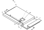
図9(A)は実施形態5に係るアンテナ装置を備えた携帯電話機の下面透視図、図9(B)は携帯電話機の上面透視図である。本実施形態に係る携帯電話機30はカメラモジュール36を備えており、図9では、携帯電話機30のカメラレンズが露出した面を下面とし、液晶表示画面が設けられた面を上面とする。
(Embodiment 5)
FIG. 9A is a bottom perspective view of a mobile phone provided with the antenna device according to the fifth embodiment, and FIG. 9B is a top perspective view of the mobile phone. The
実施形態5に係る携帯電話機30は樹脂製の筐体30Aを備えている。筐体30Aには、実施形態5に係るアンテナ装置1D、バッテリーパック31、基板32,33等が収容されている。基板32,33は、平面視でバッテリーパック31を挟んで設けられ、同軸ケーブル35により電気的に接続されている。
The
アンテナ装置1Dは、バッテリーパック31、基板32,33に対向するよう配置された金属部材としての平面導体11Aを備えている。平面導体11Aは、アンテナ装置1Dを備える携帯電話機30の筐体30Aに貼り付けられたものであってもよいし、筐体30A内部にメッキ加工等で形成された電磁波シールド部材を用いたものであってもよい。平面導体11Aは矩形状であって、基板32,33に実装された後述の電界放射型アンテナ3A,3Bと重ならないように配置されている。平面導体11Aには、短手方向に延びたスリット111Aと、スリット111Aに連結された円形状の開口部112Aとが形成されている。
The antenna device 1 </ b> D includes a
アンテナ装置1Dはコイルアンテナ2A及びチップコンデンサ4Aを備えている。実施形態1に係るコイルアンテナ2と同様に、コイルアンテナ2Aはフレキシブル基板(不図示)にコイル導体21Aが円形状に巻回されている。また、コイル導体21Aの形成面とは反対側の面においてフレキシブル基板と接するように磁性体層(不図示)が設けられている。コイルアンテナ2Aはコイル導体21Aのコイル開口部CWが、開口部112Aと重なるように平面導体11Aに設けられている。コイル導体21Aの両端部には、基板33に設けられた後述する接触ピン34A,34Bが接続されていて、接触ピン34A,34Bを介して基板33の不図示の給電部から給電される。これにより、図3で説明したように、平面導体11Aに電流が流れる。
The
また、チップコンデンサ4Aは、平面導体11Aの端部近傍にスリット111Aを跨いで設けられている。チップコンデンサ4Aは、実施形態1に係るチップコンデンサ4と同様、流れる電流に係る周波数に応じてハイインピーダンス又はローインピーダンスとなる。すなわち、平面導体11Aのスリット111Aが形成された部分は、チップコンデンサ4Aがハイインピーダンスのときには実質的に開放となり、ローインピーダンスのときには実質的に短絡される。
Further, the
基板32には、電界放射型アンテナ3A、及び平面導体11Aに接触する接触ピン32A,32Bが設けられている。不図示の給電部から、電界放射型アンテナ3Aと、接触ピン32A,32Bを介して平面導体11Aとに電流が流れることにより、電界放射型アンテナ3A及び平面導体11Aは携帯電話機30のUHF帯による通信用のアンテナ(ダイポールアンテナ)として機能する。給電部は、基板32に実装されてもよいし、基板33に実装されてもよい。
The
基板33には、電界放射型アンテナ3Bと、平面導体11Aに接触する接触ピン33A,33Bと、平面導体11Aのコイルアンテナ2Aのコイル導体両端部に接続される接触ピン34A,34Bとが設けられている。基板33には、電界放射型アンテナ3B、及び平面導体11Aに接触する接触ピン33A,33Bが設けられている。不図示の給電部から、電界放射型アンテナ3Bと、接触ピン33A,33Bを介して平面導体11Aとに電流が流れることにより、電界放射型アンテナ3B及び平面導体11Aは携帯電話機30のUHF帯による通信用のアンテナ(ダイポールアンテナ)として機能する。
The
また、基板33にはカメラモジュール36が設けられている。カメラモジュール36は、カメラレンズが平面導体11Aの開口部112Aから露出するよう設けられている。このように、開口部112Aから突出したカメラレンズを露出させることで、平面導体11Aを筐体30Aに設けても、カメラモジュール36等の他の電子部品の障害とならない。
A
このように、実施形態5では、上述の各実施形態と同様に、通信特性を劣化させることなく、平面導体11AをHF帯による通信及びUHF帯による通信の二つの通信で放射素子として用いることができる。このため、アンテナ装置1Dの部品点数を削減でき、コストダウンを図れる。また、UHF帯による通信においてスリット111A及び開口部112Aに沿って電流が流れる場合、スリット111A等の長さを考慮して平面導体11Aを設計する必要があるが、チップコンデンサ4Aによりスリット111A部分を短絡させることで、UHF帯による通信におけるスリット111A等の長さを無視でき、設計の手間を省くことができる。
As described above, in the fifth embodiment, similarly to the above-described embodiments, the
また、電界放射型アンテナ3A,3Bから出力される電流は基板32,33内の電極等を通じて、さらに同軸ケーブル35にも流れる。このため、平面導体11Aが仮にない場合であっても、基板32,33及び同軸ケーブル35によって、基板32,33中の金属部分(例えばグランド電極)が放射体として機能することにより、所謂筐体30Aのアンテナ化による特性の改善がある。しかし、基板32,33には多数のチップ部品が実装されていることなどから、その影響で特性が劣化することがある。そこで、本実施形態のように平面導体11Aに筐体30Aの電流が流れるようにすることによって特性の改善を図ることが出来る。
Further, the current output from the
また、実施形態1に係るチップコンデンサ4と同様の接続手段としての機能を有するチップコンデンサ4Aが設けられているので、電界放射型アンテナ3A,3Bから出力される電流は接続手段を介して流れることからスリット111A等に沿って流れることはない。このため、電界放射型アンテナ3A,3Bによる通信時に流れる電流が磁界放射型アンテナの磁性体層付近を流れることがなく、磁性体層での損失により電界放射型アンテナによる通信特性が劣化するのを防止できる。
In addition, since the
なお、本実施形態では、3つの電界放射型アンテナ3A,3Bを有していたが、電界放射型アンテナは1つであっても構わない。
In this embodiment, the three
以上、本発明に係るアンテナ装置及び通信端末について説明したが、本発明は、上述した各実施形態に限定されるものではなく種々の変更が可能である。例えば、接続手段は、チップコンデンサもしくは対向する裏面電極パターンからなる例を示したが、間隔を小さくしたスリット間に発生する容量を接続手段として用いてもよい。また、スリットを櫛歯状に形成することによって接続手段を構成してもよい。また、スリットの幅は開口部の幅と同じに設定してもよい。 The antenna device and the communication terminal according to the present invention have been described above, but the present invention is not limited to the above-described embodiments, and various modifications can be made. For example, the connection means is an example of a chip capacitor or an opposing back electrode pattern. However, a capacitance generated between slits with a small interval may be used as the connection means. Moreover, you may comprise a connection means by forming a slit in a comb-tooth shape. The width of the slit may be set to be the same as the width of the opening.
1,1A,1B,1C−アンテナ装置
2−コイルアンテナ(磁界結合型アンテナ)
3−電界放射型アンテナ(電界放射型アンテナ)
4−チップコンデンサ(接続手段)
5−給電部
10−基板(誘電体基板)
11−グランド導体パターン(平面導体)
12−裏面電極パターン(別の平面導体)
21−コイル導体
22−フレキシブル基板
23−磁性体シート
111−スリット
112−開口部
CW−コイル開口部
C2,C3−浮遊容量
1, 1A, 1B, 1C-antenna device 2-coil antenna (magnetically coupled antenna)
3- Field Emission Antenna (Field Emission Antenna)
4-chip capacitor (connecting means)
5-Power supply unit 10-Substrate (dielectric substrate)
11-Ground conductor pattern (planar conductor)
12-Back electrode pattern (another flat conductor)
21-coil conductor 22-flexible substrate 23-magnetic material sheet 111-slit 112-opening CW-coil opening C2, C3-floating capacitance
Claims (7)
第1周波数帯で動作し、前記平面導体を放射板として用いる電界放射型アンテナと、
磁性体層及び前記磁性体層に沿って形成されたコイル導体を有し、前記厚み方向から視て前記開口部と一部が重なる位置に配置され、前記第1周波数帯よりも低い周波数帯である第2周波数帯で動作する磁界結合型アンテナと、
前記スリットにより分断された前記平面導体の一部を電気的に接続する接続手段と、
を備え、
前記接続手段は、前記第1周波数帯に対して実質的に短絡となり、前記第2周波数帯に対して実質的に開放となる、
アンテナ装置。 A planar conductor in which an opening penetrating in the thickness direction and a slit extending from the one end to the opening are formed;
A field emission antenna that operates in a first frequency band and uses the planar conductor as a radiation plate;
A coil conductor formed along the magnetic material layer and the magnetic material layer, disposed at a position partially overlapping the opening as viewed from the thickness direction, and in a frequency band lower than the first frequency band; A magnetically coupled antenna operating in a second frequency band;
Connection means for electrically connecting a part of the planar conductor divided by the slit;
With
The connection means is substantially short-circuited with respect to the first frequency band and substantially open with respect to the second frequency band.
Antenna device.
請求項1に記載のアンテナ装置。 The connection means is a reactance element having inductivity with respect to the first frequency band and capacitive with respect to the second frequency band.
The antenna device according to claim 1.
前記平面導体の少なくとも一部は前記基板に形成された導体パターンである、
請求項1から3の何れかに記載のアンテナ装置。 Comprising a substrate on which the field emission antenna is disposed;
At least a part of the planar conductor is a conductor pattern formed on the substrate.
The antenna device according to any one of claims 1 to 3.
請求項1から4の何れかに記載のアンテナ装置。 The first frequency band is a UHF band, and the second frequency band is an HF band.
The antenna device according to claim 1.
前記基板の厚み方向で前記導体パターンに対向するよう前記基板に形成され、前記スリットと一部が対向している別の平面導体を備え、
前記接続手段は、前記平面導体及び前記別の平面導体間に形成される浮遊容量である、
請求項1に記載のアンテナ装置。 Comprising a substrate on which the field emission antenna is disposed;
Formed on the substrate to face the conductor pattern in the thickness direction of the substrate, and comprises another planar conductor partially facing the slit,
The connection means is a stray capacitance formed between the planar conductor and the another planar conductor.
The antenna device according to claim 1.
筐体と、
を備える通信端末であって、
前記筐体は金属部分を有し、前記平面導体は前記金属部分の少なくとも一部から構成される、通信端末。 An antenna device according to any one of claims 1 to 6;
A housing,
A communication terminal comprising:
The communication terminal, wherein the housing has a metal portion, and the planar conductor is composed of at least part of the metal portion.
Priority Applications (1)
| Application Number | Priority Date | Filing Date | Title |
|---|---|---|---|
| JP2012032253A JP2013168894A (en) | 2012-02-17 | 2012-02-17 | Antenna device and communication terminal having the same |
Applications Claiming Priority (1)
| Application Number | Priority Date | Filing Date | Title |
|---|---|---|---|
| JP2012032253A JP2013168894A (en) | 2012-02-17 | 2012-02-17 | Antenna device and communication terminal having the same |
Publications (1)
| Publication Number | Publication Date |
|---|---|
| JP2013168894A true JP2013168894A (en) | 2013-08-29 |
Family
ID=49178961
Family Applications (1)
| Application Number | Title | Priority Date | Filing Date |
|---|---|---|---|
| JP2012032253A Pending JP2013168894A (en) | 2012-02-17 | 2012-02-17 | Antenna device and communication terminal having the same |
Country Status (1)
| Country | Link |
|---|---|
| JP (1) | JP2013168894A (en) |
Cited By (15)
| Publication number | Priority date | Publication date | Assignee | Title |
|---|---|---|---|---|
| CN104681917A (en) * | 2013-12-03 | 2015-06-03 | 佳邦科技股份有限公司 | Double-coil antenna structure |
| WO2015133504A1 (en) * | 2014-03-07 | 2015-09-11 | 株式会社村田製作所 | Antenna equipment and electronic device |
| WO2015182638A1 (en) * | 2014-05-30 | 2015-12-03 | 株式会社村田製作所 | Antenna device and electronic device |
| JP2016123112A (en) * | 2013-09-17 | 2016-07-07 | 株式会社村田製作所 | Electronic apparatus |
| JP2016213540A (en) * | 2015-04-30 | 2016-12-15 | Tdk株式会社 | Antenna device |
| WO2017073834A1 (en) * | 2015-10-29 | 2017-05-04 | 엘지전자(주) | Mobile terminal |
| JP2017123547A (en) * | 2016-01-06 | 2017-07-13 | アルプス電気株式会社 | Antenna device and keyless entry device |
| WO2018003238A1 (en) * | 2016-06-28 | 2018-01-04 | 株式会社村田製作所 | Antenna device and electronic instrument |
| CN107546463A (en) * | 2016-06-29 | 2018-01-05 | 禾邦电子(苏州)有限公司 | NFC antenna under semi-closed metal slit environment |
| CN107871930A (en) * | 2016-09-26 | 2018-04-03 | 上海德门电子科技有限公司 | A kind of NFC antenna and its communication apparatus for being applicable fluting or open-porous metal housing |
| JP2018057006A (en) * | 2016-01-14 | 2018-04-05 | 株式会社村田製作所 | Antenna device and electronic apparatus |
| WO2018181042A1 (en) * | 2017-03-27 | 2018-10-04 | 株式会社村田製作所 | Antenna device and electronic apparatus |
| US10530057B2 (en) | 2016-09-26 | 2020-01-07 | Murata Manufacturing, Co., Ltd. | Antenna device and electronic appliance |
| CN111279552A (en) * | 2017-11-02 | 2020-06-12 | 株式会社Sk电子 | LC resonance antenna |
| JP2020102851A (en) * | 2013-10-17 | 2020-07-02 | エルジー エレクトロニクス インコーポレイティド | Mobile terminal |
-
2012
- 2012-02-17 JP JP2012032253A patent/JP2013168894A/en active Pending
Cited By (31)
| Publication number | Priority date | Publication date | Assignee | Title |
|---|---|---|---|---|
| JP2016123112A (en) * | 2013-09-17 | 2016-07-07 | 株式会社村田製作所 | Electronic apparatus |
| US11019187B2 (en) | 2013-10-17 | 2021-05-25 | Lg Electronics Inc. | Mobile terminal |
| JP2020102851A (en) * | 2013-10-17 | 2020-07-02 | エルジー エレクトロニクス インコーポレイティド | Mobile terminal |
| CN104681917A (en) * | 2013-12-03 | 2015-06-03 | 佳邦科技股份有限公司 | Double-coil antenna structure |
| WO2015133504A1 (en) * | 2014-03-07 | 2015-09-11 | 株式会社村田製作所 | Antenna equipment and electronic device |
| WO2015133503A1 (en) * | 2014-03-07 | 2015-09-11 | 株式会社村田製作所 | Antenna equipment and electronic device |
| JP5800118B1 (en) * | 2014-03-07 | 2015-10-28 | 株式会社村田製作所 | ANTENNA DEVICE AND ELECTRONIC DEVICE |
| JP5800117B1 (en) * | 2014-03-07 | 2015-10-28 | 株式会社村田製作所 | ANTENNA DEVICE AND ELECTRONIC DEVICE |
| GB2538447A (en) * | 2014-03-07 | 2016-11-16 | Murata Manufacturing Co | Antenna equipment and electronic device |
| GB2538661A (en) * | 2014-03-07 | 2016-11-23 | Murata Manufacturing Co | Antenna equipment and electronic device |
| US10270155B2 (en) | 2014-03-07 | 2019-04-23 | Murata Manufacturing Co., Ltd. | Antenna device and electronic apparatus |
| US10270156B2 (en) | 2014-03-07 | 2019-04-23 | Murata Manufacturing Co., Ltd. | Antenna device and electronic apparatus |
| US10164336B2 (en) | 2014-05-30 | 2018-12-25 | Murata Manufacturing Co., Ltd. | Antenna device and electronic apparatus |
| WO2015182638A1 (en) * | 2014-05-30 | 2015-12-03 | 株式会社村田製作所 | Antenna device and electronic device |
| JP6075511B2 (en) * | 2014-05-30 | 2017-02-08 | 株式会社村田製作所 | ANTENNA DEVICE AND ELECTRONIC DEVICE |
| JP2016213540A (en) * | 2015-04-30 | 2016-12-15 | Tdk株式会社 | Antenna device |
| KR101820471B1 (en) * | 2015-10-29 | 2018-01-19 | 엘지전자 주식회사 | Mobile terminal |
| WO2017073834A1 (en) * | 2015-10-29 | 2017-05-04 | 엘지전자(주) | Mobile terminal |
| JP2017123547A (en) * | 2016-01-06 | 2017-07-13 | アルプス電気株式会社 | Antenna device and keyless entry device |
| JP2018057006A (en) * | 2016-01-14 | 2018-04-05 | 株式会社村田製作所 | Antenna device and electronic apparatus |
| US10276936B2 (en) | 2016-01-14 | 2019-04-30 | Murata Manufacturing Co., Ltd. | Antenna device and electronic apparatus |
| JPWO2018003238A1 (en) * | 2016-06-28 | 2018-08-30 | 株式会社村田製作所 | ANTENNA DEVICE AND ELECTRONIC DEVICE |
| WO2018003238A1 (en) * | 2016-06-28 | 2018-01-04 | 株式会社村田製作所 | Antenna device and electronic instrument |
| CN107546463A (en) * | 2016-06-29 | 2018-01-05 | 禾邦电子(苏州)有限公司 | NFC antenna under semi-closed metal slit environment |
| CN107546463B (en) * | 2016-06-29 | 2024-04-02 | 禾邦电子(苏州)有限公司 | NFC antenna in semi-closed metal gap environment |
| US10530057B2 (en) | 2016-09-26 | 2020-01-07 | Murata Manufacturing, Co., Ltd. | Antenna device and electronic appliance |
| CN107871930A (en) * | 2016-09-26 | 2018-04-03 | 上海德门电子科技有限公司 | A kind of NFC antenna and its communication apparatus for being applicable fluting or open-porous metal housing |
| JP6428990B1 (en) * | 2017-03-27 | 2018-11-28 | 株式会社村田製作所 | ANTENNA DEVICE AND ELECTRONIC DEVICE |
| WO2018181042A1 (en) * | 2017-03-27 | 2018-10-04 | 株式会社村田製作所 | Antenna device and electronic apparatus |
| CN111279552A (en) * | 2017-11-02 | 2020-06-12 | 株式会社Sk电子 | LC resonance antenna |
| CN111279552B (en) * | 2017-11-02 | 2022-09-09 | 株式会社Sk电子 | LC resonance antenna |
Similar Documents
| Publication | Publication Date | Title |
|---|---|---|
| US10033104B2 (en) | Antenna device and wireless communication device | |
| JP2013168894A (en) | Antenna device and communication terminal having the same | |
| US10033089B2 (en) | Antenna device and electronic apparatus including antenna device | |
| US9997834B1 (en) | Antenna device and communication terminal apparatus | |
| JP6256600B2 (en) | ANTENNA DEVICE AND ELECTRONIC DEVICE | |
| JP5773021B2 (en) | Antenna device | |
| JP5924006B2 (en) | Antenna device | |
| US9019168B2 (en) | Frequency stabilization circuit, frequency stabilization device, antenna apparatus and communication terminal equipment, and impedance conversion element | |
| JP4934784B2 (en) | Antenna device and communication terminal device | |
| JP6311833B2 (en) | Antenna device | |
| JP5655959B2 (en) | ANTENNA DEVICE, FEEDING ELEMENT AND COMMUNICATION TERMINAL DEVICE | |
| US9634380B2 (en) | Antenna device and communication terminal device | |
| US8797225B2 (en) | Antenna device and communication terminal apparatus | |
| US9300037B2 (en) | Antenna device and antenna mounting method | |
| JP2013012936A (en) | Antenna device |