JP2013150324A - Improvement in isolation of antennas mounted on printed circuit board - Google Patents
Improvement in isolation of antennas mounted on printed circuit board Download PDFInfo
- Publication number
- JP2013150324A JP2013150324A JP2013007156A JP2013007156A JP2013150324A JP 2013150324 A JP2013150324 A JP 2013150324A JP 2013007156 A JP2013007156 A JP 2013007156A JP 2013007156 A JP2013007156 A JP 2013007156A JP 2013150324 A JP2013150324 A JP 2013150324A
- Authority
- JP
- Japan
- Prior art keywords
- cover
- antenna
- circuit
- slot
- isolation
- Prior art date
- Legal status (The legal status is an assumption and is not a legal conclusion. Google has not performed a legal analysis and makes no representation as to the accuracy of the status listed.)
- Withdrawn
Links
Images


Classifications
-
- H—ELECTRICITY
- H01—ELECTRIC ELEMENTS
- H01Q—ANTENNAS, i.e. RADIO AERIALS
- H01Q1/00—Details of, or arrangements associated with, antennas
- H01Q1/12—Supports; Mounting means
- H01Q1/22—Supports; Mounting means by structural association with other equipment or articles
- H01Q1/24—Supports; Mounting means by structural association with other equipment or articles with receiving set
-
- H—ELECTRICITY
- H01—ELECTRIC ELEMENTS
- H01Q—ANTENNAS, i.e. RADIO AERIALS
- H01Q21/00—Antenna arrays or systems
- H01Q21/28—Combinations of substantially independent non-interacting antenna units or systems
-
- H—ELECTRICITY
- H01—ELECTRIC ELEMENTS
- H01Q—ANTENNAS, i.e. RADIO AERIALS
- H01Q1/00—Details of, or arrangements associated with, antennas
- H01Q1/12—Supports; Mounting means
- H01Q1/22—Supports; Mounting means by structural association with other equipment or articles
-
- H—ELECTRICITY
- H01—ELECTRIC ELEMENTS
- H01Q—ANTENNAS, i.e. RADIO AERIALS
- H01Q1/00—Details of, or arrangements associated with, antennas
- H01Q1/36—Structural form of radiating elements, e.g. cone, spiral, umbrella; Particular materials used therewith
- H01Q1/38—Structural form of radiating elements, e.g. cone, spiral, umbrella; Particular materials used therewith formed by a conductive layer on an insulating support
-
- H—ELECTRICITY
- H01—ELECTRIC ELEMENTS
- H01Q—ANTENNAS, i.e. RADIO AERIALS
- H01Q1/00—Details of, or arrangements associated with, antennas
- H01Q1/52—Means for reducing coupling between antennas; Means for reducing coupling between an antenna and another structure
- H01Q1/521—Means for reducing coupling between antennas; Means for reducing coupling between an antenna and another structure reducing the coupling between adjacent antennas
-
- H—ELECTRICITY
- H01—ELECTRIC ELEMENTS
- H01Q—ANTENNAS, i.e. RADIO AERIALS
- H01Q1/00—Details of, or arrangements associated with, antennas
- H01Q1/52—Means for reducing coupling between antennas; Means for reducing coupling between an antenna and another structure
- H01Q1/526—Electromagnetic shields
Abstract
Description
本発明は、概して無線システムで使用されるプリント回路基板に関する。特に、シールドカバー(shielding cover)のようなカバーに覆われた処理回路及び少なくとも1つのアンテナを同じ回路基板上に有する基板に関する。 The present invention relates generally to printed circuit boards for use in wireless systems. In particular, it relates to a substrate having a processing circuit covered by a cover, such as a shielding cover, and at least one antenna on the same circuit board.
無線通信分野では、送信回路の能力を増加させ、カバレッジを改善するために、MIMO(Multiple Input Multiple Output)回路の更なる使用が行われている。その結果、より多くの数のアンテナが使用される。アンテナがプリント回路基板(PCB:printed circuit board)に直接プリントされた場合又は配置された場合、これは、接地面(ground plane)において、他のアンテナの動作に潜在的に影響を与える電流と、アンテナの近くに配置された処理回路の電流とを引き起こす。従って、アンテナの性能を劣化させずに、電流の漏れを制限するために、素子を相互に分離(isolate)する必要がある。更に、MIMOシステムの場合、MIMOシステムの最適な性能を提供するためには、所要の信号からの非相関性(decorrelation)のレベルを得るために、アンテナはかなり分離されなければならない。しかし、基板上の空間が限られており、分離(isolation)の制限は非常に強い。更に、複数の周波数帯域で動作するシステムの場合、周波数帯域の全ての無線の正確な共存を可能にするように、帯域の間の分離は最も頻繁に必要になる。 In the field of wireless communication, further use of multiple input multiple output (MIMO) circuits is being made in order to increase the capacity of transmission circuits and improve coverage. As a result, a greater number of antennas are used. If the antenna is printed or placed directly on a printed circuit board (PCB), this can cause currents in the ground plane that potentially affect the operation of other antennas, Causing a current in a processing circuit located near the antenna. Therefore, it is necessary to isolate the elements from each other in order to limit current leakage without degrading the performance of the antenna. Furthermore, in the case of a MIMO system, in order to provide optimal performance of the MIMO system, the antennas must be significantly separated to obtain a level of decorrelation from the required signal. However, the space on the substrate is limited, and the isolation limit is very strong. Furthermore, for systems operating in multiple frequency bands, separation between the bands is most often required to allow for the correct coexistence of all radios in the frequency band.
更に、放射レベルを低減することにより、電磁気干渉及び無線周波数を低減するために、処理回路の上部に固定されたシールドカバー(shielding cover)が頻繁に使用される。現在の無線システムがしばしばマルチバンド及びマルチモードになっているため、この使用はますます頻繁になっている。このことは、より大きい干渉問題をもたらす。更に、無線デバイスの小型化への傾向及び同じ基板上の複数の回路への傾向は、改善した分離及びシールドを必要とする。更に、電磁波及び無線周波数のレベルに関する規制がますます制限されている。 In addition, a shielding cover secured to the top of the processing circuit is frequently used to reduce electromagnetic interference and radio frequency by reducing radiation levels. This use is becoming increasingly frequent as current wireless systems are often multiband and multimode. This leads to a larger interference problem. Furthermore, the trend toward miniaturization of wireless devices and the trend to multiple circuits on the same substrate requires improved isolation and shielding. Furthermore, regulations regarding the level of electromagnetic waves and radio frequencies are increasingly restricted.
特に米国特許出願第2003/0193437において、アンテナの相互カップリングを低減し、表面電流の漏れを制限するために、2つのアンテナの間にスロットを使用することが知られている。しかし、この種類の分離は、表層(surface)を必要とする。この理由は、スロットの長さが特にλ/4に等しいからである。ただし、λは回路の動作周波数の波長である。従って、2.4GHzの動作周波数では、波長は約30mmである。 In particular, in US patent application 2003/0193437, it is known to use a slot between two antennas to reduce antenna mutual coupling and limit surface current leakage. However, this type of separation requires a surface. This is because the slot length is particularly equal to λ / 4. Where λ is the wavelength of the operating frequency of the circuit. Therefore, at an operating frequency of 2.4 GHz, the wavelength is about 30 mm.
従って、本発明は、プリント回路基板のサイズを増加させることなく、更なる構成要素又は機械部品を追加することなく、必要な分離が得られることを可能にする、前述の問題への低コストの対策を提案する。 Thus, the present invention provides a low cost to the aforementioned problem that allows the necessary isolation to be obtained without increasing the size of the printed circuit board and without adding additional components or mechanical parts. Suggest measures.
本発明は、少なくとも1つのアンテナと、処理回路と、処理回路を覆うカバーとを同じ基板上に有する回路に関し、アンテナとカバーとの間に、基板上に部分的に実現され、カバー上に部分的に実現されたスロットライン(slot line)により形成された少なくとも1つの分離要素を有することを特徴とする。 The present invention relates to a circuit having at least one antenna, a processing circuit, and a cover covering the processing circuit on the same substrate, and is partially realized on the substrate between the antenna and the cover, and is partially on the cover. Characterized in that it has at least one separating element formed by a slot line realized in a practical manner.
一実施例によれば、スロットラインは、第3のスロットラインにより相互接続された第1及び第2のスロットラインを有する。第1及び第2のスロットラインは、L1+L’1がL2+L’2と等しくなるように又は異なるように、基板上にそれぞれL1及びL2の第1の長さを有し、カバー上にそれぞれL’1及びL’2の第2の長さを有する。第1及び第2のスロットラインの長さは、λg/4に近く、λgは動作周波数の波長である。 According to one embodiment, the slot line has first and second slot lines interconnected by a third slot line. The first and second slot lines have a first length of L1 and L2 on the substrate, respectively, so that L1 + L′ 1 is equal to or different from L2 + L′ 2, and on the cover Each have a second length of L′ 1 and L′ 2. The length of the first and second slot lines is close to λg / 4, where λg is the wavelength of the operating frequency.
本発明の他の特徴及び利点は、図面を参照して具現される実施例の説明を読むことで明らかになる。 Other features and advantages of the present invention will become apparent upon reading the description of the embodiments embodied with reference to the drawings.
本発明について、セットトップボックスに統合可能な2×2のMIMO回路を備えた2.4GHzの帯域で動作する2つのアンテナを有する用途で使用されるプリント回路基板を参照することにより説明する。しかし、この実施例は単なる情報として提供されており、本発明の範囲を離れることなく、多くの方法で変更されてもよいことが、当業者に明らかである。これは、移動デバイス、タブレット、ゲートウェイ等のような無線で動作する多くのデバイスで使用されてもよい。 The present invention will be described with reference to a printed circuit board used in an application having two antennas operating in the 2.4 GHz band with a 2 × 2 MIMO circuit that can be integrated into a set top box. However, it will be apparent to those skilled in the art that this embodiment is provided for information only and may be modified in many ways without departing from the scope of the present invention. This may be used in many devices that operate wirelessly, such as mobile devices, tablets, gateways, etc.
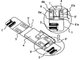
図1に示すように、基板1上において、基板のそれぞれの端に2つのアンテナ2及び3が実現されている。2つのアンテナ2及び3の間に、2つのアンテナにより受信及び放射された信号のための処理回路が同じ基板1上に搭載されている。この処理回路は、アンテナの処理回路を分離しつつ、電磁干渉及び無線周波数干渉を低減するために、シールドカバー4により覆われている。
As shown in FIG. 1, on the substrate 1, two
既知の方法では、シールドカバー4は、一般的に、打ち抜き加工(stamping)により作られ、すなわち、構成要素表面実装技術(component surface mount technology)を使用することにより、構成要素と同じ組み立て手順の間に基板に固定される。カバーは、構成要素の検査及び修理を可能にするために、単一の部分又は2つの部分に実現されてもよい。 In a known manner, the shield cover 4 is typically made by stamping, i.e. during the same assembly procedure as the component by using component surface mount technology. Fixed to the substrate. The cover may be implemented in a single part or in two parts to allow inspection and repair of the component.
図1に示すように、1つのアンテナ(すなわち、図示の実施例のアンテナ2)は、この基板の端に沿ってプリント回路基板1に直接実現された2つの分離スロット(isolation slot)5及び5’により、カバー4から分離されている。しかし、図1に示すように、第2のアンテナ3は、カバー4の近くに配置される。プリント回路基板の表面を増加させないため、図1の拡大部分に示すように、本発明によれば、アンテナ3とカバー4との間の分離要素は、基板1上に部分的に実現され、カバー4上に部分的に実現される。より正確には、拡大部分に示すように、分離手段は、それぞれ2つの部分(すなわち、6a、6b、6’a、6’b)を有する2つのスロットライン(slot line)6及び6’により構成される。部分6a及び6’aはプリント回路基板1に実現され、部分6b及び6’bはカバー4に実現される。これらの2つのスロットライン6及び6’がプロント回路のレベルでショートされるのを妨げるために、これらはスロット7により相互接続される。
As shown in FIG. 1, one antenna (ie,
必要な分離を得るために、各スロット6、6’の合計の長さは、特にλg/4に等しくなるように選択される。ただし、λgは動作周波数の波長である。従って、部分6a及び6’aがそれぞれL1及びL2の長さを有し、部分6b及び6’bがそれぞれL’1及びL’2の長さを有する場合、スロット6及び6’の合計の長さは、L1+L’1≒L2+L’2≒λg/4になるようにならなければならない。しかし、L1+L’1≠L2+L’2のような対策も、本発明の範囲内に入る。
In order to obtain the required separation, the total length of each
図1に示すようなデバイスは、HFSS(Ansys)の名前で知られている3D電磁気シミュレーションツールでシミュレーションされた。第1のシミュレーションは、本発明による分離要素なしに実現され、第2のシミュレーションは、図1に示すような分離要素を用いて実現された。 The device as shown in FIG. 1 was simulated with a 3D electromagnetic simulation tool known by the name of HFSS (Ansys). The first simulation was realized without a separation element according to the present invention, and the second simulation was realized using a separation element as shown in FIG.
図2に示すように、本発明による分離要素なしでは、2.4GHzの帯域での分離レベルは、最悪の場合に約14dBになることが分かる。 As shown in FIG. 2, it can be seen that without the separation element according to the present invention, the separation level in the 2.4 GHz band is about 14 dB in the worst case.
図3に示すように、2つのアンテナの間の分離の応答は、2.4GHzの帯域で約-20dBであり、これは5dBより大きい増加を示している。アンテナ3が励起されたときの表面電流のラインは、これらの分離要素なしに取得された結果に対して分離要素6及び6’の効率性を示している。従って、2つのアンテナの間のカップリング(coupling)の低減が得られ、アンテナ3の動作が基板上のその位置にあまり敏感でなくなり、システムの全体の接地(ground)に対するその接地面を接続する方法にあまり敏感でなくなる。
As shown in FIG. 3, the isolation response between the two antennas is about -20 dB in the 2.4 GHz band, indicating an increase of more than 5 dB. The line of surface current when the
分離要素を実現するスロットラインは、分離レベル又は分離帯域を増加させるために、同じ長さを有してもよく、異なる長さを有してもよいことが、当業者に明らかである。更に、スロットは、L形状若しくはC形状又はその位置に互換性のある他の形状を有してもよい。 It will be apparent to those skilled in the art that the slot lines that implement the separation elements may have the same length or different lengths to increase the separation level or separation band. Further, the slot may have an L shape or a C shape or other shapes that are compatible in position.
1 基板
2 アンテナ
3 アンテナ
4 シールドカバー
5 分離スロット
5’ 分離スロット
6 スロットライン
6’ スロットライン
7 スロット
1 Board
2 Antenna
3 Antenna
4 Shield cover
5 Separation slot
5 'separation slot
6 slot lines
6 'slot line
7 slots
Claims (4)
前記アンテナと前記カバーとの間に、前記基板上に部分的に実現され、前記カバー上に部分的に実現されたスロットラインにより形成された少なくとも1つの分離要素を有することを特徴とする回路。 A circuit having at least one antenna, a processing circuit, and a cover covering the processing circuit on the same substrate,
A circuit comprising between the antenna and the cover, at least one isolation element partially realized on the substrate and formed by a slot line partially realized on the cover.
Applications Claiming Priority (2)
| Application Number | Priority Date | Filing Date | Title |
|---|---|---|---|
| FR1250571 | 2012-01-20 | ||
| FR1250571A FR2986110A1 (en) | 2012-01-20 | 2012-01-20 | IMPROVEMENT IN THE INSULATION OF ANTENNAS MOUNTED ON A CIRCUIT BOARD |
Publications (2)
| Publication Number | Publication Date |
|---|---|
| JP2013150324A true JP2013150324A (en) | 2013-08-01 |
| JP2013150324A5 JP2013150324A5 (en) | 2016-03-03 |
Family
ID=47355969
Family Applications (1)
| Application Number | Title | Priority Date | Filing Date |
|---|---|---|---|
| JP2013007156A Withdrawn JP2013150324A (en) | 2012-01-20 | 2013-01-18 | Improvement in isolation of antennas mounted on printed circuit board |
Country Status (11)
| Country | Link |
|---|---|
| US (1) | US9203164B2 (en) |
| EP (1) | EP2618422B1 (en) |
| JP (1) | JP2013150324A (en) |
| KR (1) | KR20130085998A (en) |
| CN (1) | CN103219589A (en) |
| AU (1) | AU2013200121A1 (en) |
| BR (1) | BR102013001240A2 (en) |
| FR (1) | FR2986110A1 (en) |
| HK (1) | HK1188036A1 (en) |
| PT (1) | PT2618422E (en) |
| TW (1) | TW201332213A (en) |
Families Citing this family (4)
| Publication number | Priority date | Publication date | Assignee | Title |
|---|---|---|---|---|
| FR2990591A1 (en) | 2012-05-14 | 2013-11-15 | Thomson Licensing | METHOD OF MAKING A LINE-SLIT ON A MULTILAYER SUBSTRATE AND MULTI-LAYER PRINTED CIRCUIT COMPRISING AT LEAST ONE LINE-SLIT REALIZED ACCORDING TO SAID METHOD AND USED AS AN INSULATED SLOT OR ANTENNA |
| TWI543447B (en) | 2013-09-09 | 2016-07-21 | 鴻海精密工業股份有限公司 | Antenna |
| CN104466400B (en) * | 2013-09-24 | 2017-06-20 | 富士康(昆山)电脑接插件有限公司 | Antenna |
| US9799953B2 (en) | 2015-03-26 | 2017-10-24 | Microsoft Technology Licensing, Llc | Antenna isolation |
Family Cites Families (10)
| Publication number | Priority date | Publication date | Assignee | Title |
|---|---|---|---|---|
| US6624789B1 (en) * | 2002-04-11 | 2003-09-23 | Nokia Corporation | Method and system for improving isolation in radio-frequency antennas |
| JP3916068B2 (en) * | 2002-11-06 | 2007-05-16 | ソニー・エリクソン・モバイルコミュニケーションズ株式会社 | Wireless device |
| JP3784807B2 (en) | 2004-02-24 | 2006-06-14 | 株式会社エヌ・ティ・ティ・ドコモ | Microstrip antenna |
| JP4666998B2 (en) | 2004-10-25 | 2011-04-06 | 京セラ株式会社 | Communication equipment |
| US7342550B2 (en) | 2005-06-17 | 2008-03-11 | Cushcraft Corporation | Rugged, metal-enclosed antenna |
| TW200816556A (en) | 2006-09-21 | 2008-04-01 | P Two Ind Inc | Integration module of antenna and connector |
| FR2910182A1 (en) | 2006-12-18 | 2008-06-20 | Thomson Licensing Sas | IMPROVEMENT OF PLANAR ANTENNAS WITH RADIANT SLOT |
| EP1950834B1 (en) | 2007-01-24 | 2012-02-29 | Panasonic Corporation | Wireless module with integrated slot antenna |
| US8085202B2 (en) * | 2009-03-17 | 2011-12-27 | Research In Motion Limited | Wideband, high isolation two port antenna array for multiple input, multiple output handheld devices |
| CN201845871U (en) * | 2010-10-29 | 2011-05-25 | 华南理工大学 | Two-unit-broadband MIMO (multiple input multiple output) antenna array |
-
2012
- 2012-01-20 FR FR1250571A patent/FR2986110A1/en not_active Withdrawn
- 2012-12-19 EP EP12198080.9A patent/EP2618422B1/en not_active Not-in-force
- 2012-12-19 PT PT121980809T patent/PT2618422E/en unknown
-
2013
- 2013-01-10 AU AU2013200121A patent/AU2013200121A1/en not_active Abandoned
- 2013-01-11 TW TW102100995A patent/TW201332213A/en unknown
- 2013-01-17 BR BRBR102013001240-8A patent/BR102013001240A2/en not_active IP Right Cessation
- 2013-01-18 US US13/744,495 patent/US9203164B2/en not_active Expired - Fee Related
- 2013-01-18 KR KR1020130005995A patent/KR20130085998A/en not_active Application Discontinuation
- 2013-01-18 JP JP2013007156A patent/JP2013150324A/en not_active Withdrawn
- 2013-01-21 CN CN2013100214468A patent/CN103219589A/en active Pending
-
2014
- 2014-01-24 HK HK14100790.6A patent/HK1188036A1/en not_active IP Right Cessation
Also Published As
| Publication number | Publication date |
|---|---|
| EP2618422A1 (en) | 2013-07-24 |
| TW201332213A (en) | 2013-08-01 |
| US9203164B2 (en) | 2015-12-01 |
| PT2618422E (en) | 2014-09-15 |
| US20130187823A1 (en) | 2013-07-25 |
| KR20130085998A (en) | 2013-07-30 |
| CN103219589A (en) | 2013-07-24 |
| FR2986110A1 (en) | 2013-07-26 |
| HK1188036A1 (en) | 2014-04-17 |
| AU2013200121A1 (en) | 2013-08-22 |
| BR102013001240A2 (en) | 2013-12-17 |
| EP2618422B1 (en) | 2014-08-06 |
Similar Documents
| Publication | Publication Date | Title |
|---|---|---|
| US8659482B2 (en) | MIMO antenna having plurality of isolation adjustment portions | |
| US9768506B2 (en) | Multi-antennna isolation adjustment | |
| JP6282653B2 (en) | Printed circuit board antenna and terminal | |
| US9300055B2 (en) | Mobile device with two antennas and antenna switch modules | |
| JP2013051644A (en) | Antenna device and electronic apparatus comprising the same | |
| EP3032645B1 (en) | An assembly of circuit boards and electronic device comprising said assembly | |
| TWI481117B (en) | Antenna system | |
| US9455490B2 (en) | Communication device integrally formed with antenna and mask | |
| JP2013150324A (en) | Improvement in isolation of antennas mounted on printed circuit board | |
| US9698469B2 (en) | Antenna structure and wireless communication device using the same | |
| US9257755B2 (en) | Apparatus for controlling electric field distribution by utilizing short trace structures | |
| US20150214618A1 (en) | Communication device and antenna element therein | |
| US20210126355A1 (en) | Antenna structure | |
| CN102769472A (en) | Wireless communication device | |
| US10727588B2 (en) | Mobile device | |
| JP7158402B2 (en) | Antenna and terminal | |
| US20150171521A1 (en) | High gain antenna structure | |
| US9960486B2 (en) | Circuit board for an antenna assembly | |
| EP3343696A1 (en) | Antenna device for reducing antenna correlation of multiple-input multiple-output system, and terminal | |
| KR20200083166A (en) | an antenna for vehicle including a horizontal beam small antenna for inter-vehicle communication | |
| WO2018230096A1 (en) | Antenna device and wireless communication device | |
| JP2024005970A (en) | wireless communication device | |
| JP2013012936A (en) | Antenna device |
Legal Events
| Date | Code | Title | Description |
|---|---|---|---|
| A521 | Written amendment |
Free format text: JAPANESE INTERMEDIATE CODE: A523 Effective date: 20160114 |
|
| A621 | Written request for application examination |
Free format text: JAPANESE INTERMEDIATE CODE: A621 Effective date: 20160114 |
|
| A761 | Written withdrawal of application |
Free format text: JAPANESE INTERMEDIATE CODE: A761 Effective date: 20160325 |