JP2013115035A - Luminous keyboard - Google Patents
Luminous keyboard Download PDFInfo
- Publication number
- JP2013115035A JP2013115035A JP2011280053A JP2011280053A JP2013115035A JP 2013115035 A JP2013115035 A JP 2013115035A JP 2011280053 A JP2011280053 A JP 2011280053A JP 2011280053 A JP2011280053 A JP 2011280053A JP 2013115035 A JP2013115035 A JP 2013115035A
- Authority
- JP
- Japan
- Prior art keywords
- thin film
- light
- key
- keyboard according
- circuit board
- Prior art date
- Legal status (The legal status is an assumption and is not a legal conclusion. Google has not performed a legal analysis and makes no representation as to the accuracy of the status listed.)
- Pending
Links
Images


Classifications
-
- H—ELECTRICITY
- H01—ELECTRIC ELEMENTS
- H01H—ELECTRIC SWITCHES; RELAYS; SELECTORS; EMERGENCY PROTECTIVE DEVICES
- H01H13/00—Switches having rectilinearly-movable operating part or parts adapted for pushing or pulling in one direction only, e.g. push-button switch
- H01H13/70—Switches having rectilinearly-movable operating part or parts adapted for pushing or pulling in one direction only, e.g. push-button switch having a plurality of operating members associated with different sets of contacts, e.g. keyboard
- H01H13/83—Switches having rectilinearly-movable operating part or parts adapted for pushing or pulling in one direction only, e.g. push-button switch having a plurality of operating members associated with different sets of contacts, e.g. keyboard characterised by legends, e.g. Braille, liquid crystal displays, light emitting or optical elements
-
- H—ELECTRICITY
- H01—ELECTRIC ELEMENTS
- H01H—ELECTRIC SWITCHES; RELAYS; SELECTORS; EMERGENCY PROTECTIVE DEVICES
- H01H2219/00—Legends
- H01H2219/036—Light emitting elements
- H01H2219/044—Edge lighting of layer
-
- H—ELECTRICITY
- H01—ELECTRIC ELEMENTS
- H01H—ELECTRIC SWITCHES; RELAYS; SELECTORS; EMERGENCY PROTECTIVE DEVICES
- H01H2219/00—Legends
- H01H2219/054—Optical elements
- H01H2219/06—Reflector
-
- H—ELECTRICITY
- H01—ELECTRIC ELEMENTS
- H01H—ELECTRIC SWITCHES; RELAYS; SELECTORS; EMERGENCY PROTECTIVE DEVICES
- H01H2219/00—Legends
- H01H2219/054—Optical elements
- H01H2219/062—Light conductor
-
- H—ELECTRICITY
- H01—ELECTRIC ELEMENTS
- H01H—ELECTRIC SWITCHES; RELAYS; SELECTORS; EMERGENCY PROTECTIVE DEVICES
- H01H2229/00—Manufacturing
- H01H2229/002—Screen printing
-
- H—ELECTRICITY
- H01—ELECTRIC ELEMENTS
- H01H—ELECTRIC SWITCHES; RELAYS; SELECTORS; EMERGENCY PROTECTIVE DEVICES
- H01H2229/00—Manufacturing
- H01H2229/024—Packing between substrate and membrane
- H01H2229/028—Adhesive
-
- H—ELECTRICITY
- H01—ELECTRIC ELEMENTS
- H01H—ELECTRIC SWITCHES; RELAYS; SELECTORS; EMERGENCY PROTECTIVE DEVICES
- H01H3/00—Mechanisms for operating contacts
- H01H3/02—Operating parts, i.e. for operating driving mechanism by a mechanical force external to the switch
- H01H3/12—Push-buttons
- H01H3/122—Push-buttons with enlarged actuating area, e.g. of the elongated bar-type; Stabilising means therefor
- H01H3/125—Push-buttons with enlarged actuating area, e.g. of the elongated bar-type; Stabilising means therefor using a scissor mechanism as stabiliser
Abstract
Description
本発明は、キーボードに関し、より詳しくは、発光機能を備えたキーボードに関する。 The present invention relates to a keyboard, and more particularly to a keyboard having a light emitting function.
ここ数年来、情報産業の急速な発展迅速により、多くのユーザーが異なる環境で、ノート型パソコン、携帯電話、PDA等といったポータブルタイプの情報装置を使用する可能性がある。しかし、光線が弱い環境では、ユーザーはキーボードキーに標示された数字や文字がはっきり見えない可能性があることで、作業が困難となり、重篤な場合には、無理にキー標示を識別しようとして視力を損なうことすらある。このため、発光キーボードを発表することで、光線不足な場所でのキーボードを使用するユーザーの不便さを改善することができる。更には、異なる発光配置により、発光キーボード使用の情報装置の見栄えを一層美しくして、販路拡張が可能となる。 In recent years, due to the rapid development of the information industry, many users may use portable information devices such as notebook computers, mobile phones, PDAs, etc. in different environments. However, in an environment where the light is weak, the user may not be able to clearly see the numbers and letters on the keyboard keys, making it difficult to work. It can even impair your vision. For this reason, announcing the light emitting keyboard can improve the inconvenience of the user who uses the keyboard in a place where light rays are insufficient. Furthermore, the different light emission arrangement makes the appearance of the information device using the light emitting keyboard more beautiful, and the sales channel can be expanded.
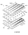
図1は公知の発光キーボードの構造断面の概略図である。発光キーボード1は光反射板11、導光板12、金属底板13、薄膜回路基板14、複数のキー15、及び発光素子16を含み、薄膜回路基板14は下層板141、上層板142、及び下層板141と上層板142の間にある中層板143を含み、下層板141、中層板143、及び上層板142は何れも透明な導光材質で製造され、透明な導光材質はポリカーボネート(PC)、又はポリエチレン・テレフタレート(PET)等でよい。
FIG. 1 is a schematic view of a cross-sectional structure of a known light-emitting keyboard. The
図2は図1に示された発光キーボードの薄膜回路基板の分解斜視図で、下層板141は複数の銀ペースト回路14111と複数の下接点14112で構成された第1回路パターン1411を備え、上層板142は複数の銀ペースト回路14211と複数の下接点14212で構成された第2回路パターン1421を備え、また、中層板143は複数の下接点14122と複数の上接点14212に対応する接点開孔1431を備え、各上接点14212とこれに対応する下接点14112は共に薄膜スイッチ144を形成する。
2 is an exploded perspective view of the thin-film circuit board of the light-emitting keyboard shown in FIG. 1. The
また、キー底板13は薄膜回路基板14の下方に取り付けられ、複数の貫通孔131、第1固定構造132、及び第2固定構造133を有する。各キー15はキーキャップ151、弾性体152、及び鋏型連接部材153を含み、キーキャップ151は第1キーキャップ固定構造1511と第2キーキャップ固定構造1512を含む。鋏型連接部材153は第1フレーム1531と第2フレーム1532を含む。また、弾性体152はキーキャップ151と薄膜回路基板141の間にある。
The
薄膜回路基板14にはそれぞれ第1固定構造132と第2固定構造133が貫通するホール145とホール146があり、第1フレーム1531の一端1531Aを第2固定構造133に連接し、他端1531Bを第1キーキャップ固定構造1511に連接することができ、また、第2フレーム1532の一端1532Aを第1固定構造132に連接し、他端1532Bを第2キーキャップ固定構造1512に連接することができる。
The thin film circuit board 14 has a
何れかのキー15が押下されて、キー底板13に対向して下方に移動すると、鋏型連接部材153の第1フレーム1531と第2フレーム1532が開いた状態から折り畳まれた状態となり、下方に移動するキーキャップ15は弾性体152を圧迫してこれに対応する上接点14212に当接させ、さらにこれに対応する上接点14212が対応する接点孔1431から対応する下接点14122に接触することによって、対応する薄膜スイッチ144が電気的に導通されて、発光キーボード1が対応するキー信号を生じる。キー15がこれ以上押下されなくなると、キーキャップ151は弾性体152の弾性力によって、キー底板13に対向して上方に移動する。この時、第1フレーム2021と第2フレーム2022は、折り畳まれた状態から開いた状態となり、キーキャップ151が元の位置に戻る。
When one of the
さらに、発光素子16は導光板12の側辺に取り付けられ、光線を導光板12に入射する。導光板12は光反射板11に取り付けられ、その下表面には光線を集光し乱反射させるための複数の導光点121がある。複数の導光点121は複数のキー15に対応する位置に応じて取り付けられる。光線が導光板12に入射すると、光線は導光板12全体に拡散され、複数の導光点121は導光板12がインク素材である関係上、光線を上下に乱反射させ、上に乱反射した光線はキー底板13の複数の貫通孔131と薄膜回路基板14を順番に通過して複数のキー15に投射され、下に乱反射した光線はさらに光反射板11のをサポートで光線を上向きに反射させて、発光素子16から提供された光線を余すところ無く利用することができる。上述したように、複数のキー15に発光効果が生じる。
Further, the
しかしながら、前述した公知の技術では、公知の発光キーボード1には下記の欠点がある。
一、光反射板11は複数の導光点121から下向きに乱反射した光線を上向きに反射させるのをサポートすることができるが、公知の発光キーボード1の光反射板11の素材は光線を透過させることができるため、複数の導光点121から下向きに乱反射した一部の光線が光反射板11を透過して光量の流失を来たす。
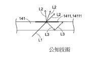
二、図3は図2に示された薄膜回路基板の下層板における光路の概略図である。複数の銀ペースト回路14211を含んだ第1回路パターン1411が下層板141の上表面に取り付けられるが、前記銀ペースト回路14211が光線を集光し乱反射させる性質を持つことから、発光素子16から提供された光線L1はキー底板13の複数の貫通孔131から下層板141に進入した後、図の光線L2のように、第1回路パターン1411の銀ペースト回路14211が発光状態となる。しかし、大部分の銀ペースト回路14211の取り付けが複数のキー15に対応していないため、本来、複数のキー15を発光させるのに使用されるべき光量が銀ペースト回路14211の特性で消耗されてしまう。即ち、本来、光線L1の光量の大半がキー15に獲得されるべきだが、銀ペースト回路14211の特性によって光線L2の光量が消耗されるため、発光キーボード1は残された光線L3の光量しか利用できず、発光キーボード1上の複数のキー15は光量が不足する状況を来たす。
However, in the known technology described above, the known light-emitting
First, the
2 and 3 are schematic views of the optical path in the lower layer plate of the thin film circuit board shown in FIG. A
さらに、図4は別の公知の発光キーボードの構造断面の概略図である。本公知の発光キーボード大体図1に示されたものに類似するので、ここではこれ以上詳述しないこととする。本公知の発光キーボードと前述公知の発光キーボードの相違点は次のとおりである。発光素子96は薄膜回路基板945の下層板941の側辺に取り付けられ、下層板941は導光素材で製作され、下層板941上には光線を集光し乱反射させる複数の導光点921があるため、薄膜回路基板94の下層板941には導光機能があり、前述公知の発光キーボード内の光反射板11や導光板12は最早必要が無く、ひいては発光キーボードを一層薄形化させる。
Further, FIG. 4 is a schematic view of the cross section of another known light-emitting keyboard. The known light-emitting keyboard is generally similar to that shown in FIG. 1 and will not be described in further detail here. Differences between the known light-emitting keyboard and the above-mentioned known light-emitting keyboard are as follows. The
然しながら、図4に示された発光キーボードは依然として前述の公知の発光キーボードにおける2つの欠点があり、薄膜回路基板94にはそれぞれキー底板93の第1固定構造932と第2固定構造933が貫通するためのホール945とホール946があり、薄膜回路基板94の下層板941の導光作用が連続されず、即ち、発光素子96から提供された光線がホール945又はホール946に当たると、前進が中断されるため、発光キーボード9の発光効率が大幅に低下する。よって、公知の発光キーボード1、9は何れも光の使用効率が不良で改善の余地がある。
However, the light-emitting keyboard shown in FIG. 4 still has the two disadvantages of the above-mentioned known light-emitting keyboard, and the
本発明は、このような従来の問題に鑑みてなされたものである。上記課題解決のため、本発明は、光使用効率が高められる発光キーボードを提供することを主目的とする。 The present invention has been made in view of such conventional problems. In order to solve the above problems, it is a main object of the present invention to provide a light-emitting keyboard with improved light use efficiency.
上記課題を解決し、目的を達成するために、好ましい実施形態では、本発明に係る発光キーボードは、
光線を発光キーボードに提供するための少なくとも1つの発光素子と、
薄膜回路基板と、
前記複数の薄膜スイッチに対応し導通するための複数のキーと、
前記複数のキーをその上に連接させ、前記複数のキーに対応する複数の貫通孔を有し、前記複数のキーと前記薄膜回路基板の間にあるキー底板と、
を含み、且つ前記薄膜回路基板は、
第1回路パターンと複数の導光点を有し、前記第1回路パターンには複数の下接点があり、前記複数の導光点は前記発光素子から提供された光線を集光して乱反射させ、前記複数の導光点が上向きに乱反射する光量を増加させるための第1薄膜と第2薄膜を含む下層板と、
第2回路パターンを有し、前記第2回路パターン上に前記複数の下接点に対応する複数の上接点があり、前記各上接点とこれに対応する前記下接点との間に間隔があり、前記対応する下接点と共に薄膜スイッチを形成する上層板と、
を含むことを特徴とする。
In order to solve the above-described problems and achieve the object, in a preferred embodiment, a light-emitting keyboard according to the present invention includes:
At least one light emitting element for providing light to the light emitting keyboard;
A thin film circuit board;
A plurality of keys for conducting in correspondence with the plurality of thin film switches;
A plurality of through holes corresponding to the plurality of keys, the key bottom plate being located between the plurality of keys and the thin film circuit board;
And the thin film circuit board comprises:
The first circuit pattern has a plurality of light guide points, the first circuit pattern has a plurality of bottom contacts, and the light guide points collect and diffusely reflect the light beam provided from the light emitting element. A lower layer plate including a first thin film and a second thin film for increasing the amount of light that the plurality of light guide points diffusely reflect upward,
A plurality of upper contacts corresponding to the plurality of lower contacts on the second circuit pattern, and there is an interval between each upper contact and the corresponding lower contact; An upper plate forming a thin film switch with the corresponding lower contact;
It is characterized by including.
好ましい実施例では、前記第1薄膜と前記第2薄膜は導光薄膜であることを特徴とする。 In a preferred embodiment, the first thin film and the second thin film are light guiding thin films.
好ましい実施例では、前記複数の導光点は前記第1薄膜と前記第2薄膜の間に設けられることを特徴とする。 In a preferred embodiment, the plurality of light guide points are provided between the first thin film and the second thin film.
好ましい実施例では、前記複数の導光点は、スクリーン印刷工程、熱圧着工程、又は射出工程により、前記第1薄膜と前記第2薄膜のうちの何れか一方に設けられることを特徴とする。 In a preferred embodiment, the plurality of light guide points are provided in any one of the first thin film and the second thin film by a screen printing process, a thermocompression bonding process, or an injection process.
好ましい実施例では、前記下層板は更に、前記第1薄膜と前記第1回路パターンの間に取り付けられて前記第1薄膜で得られた光線が前記第1薄膜内で全反射を起こす確率を高める間隔薄膜を含むことを特徴とする。 In a preferred embodiment, the lower layer plate is further mounted between the first thin film and the first circuit pattern to increase the probability that the light beam obtained from the first thin film causes total reflection in the first thin film. It includes a gap thin film.
好ましい実施例では、前記間隔薄膜は印刷工程、めっき皮膜工程、接着工程、又は熱圧着工程により、前記第1薄膜上に形成されることを特徴とする。 In a preferred embodiment, the gap thin film is formed on the first thin film by a printing process, a plating film process, an adhesion process, or a thermocompression bonding process.
好ましい実施例では、前記第1薄膜と前記第2薄膜の間には、前記第1薄膜と前記第2薄膜を相互に貼り合せて、光線を透過させることが可能な透明の接着剤があることを特徴とする。 In a preferred embodiment, between the first thin film and the second thin film, there is a transparent adhesive capable of transmitting the light beam by bonding the first thin film and the second thin film to each other. It is characterized by.
好ましい実施例では、前記導光薄膜はポリエチレン・テレフタレート(PET)素材、ポリカーボネート(PC)素材、又はポリメタクリル酸メチル樹脂(PMMA)素材で製作されることを特徴とする。 In a preferred embodiment, the light guide thin film is made of a polyethylene terephthalate (PET) material, a polycarbonate (PC) material, or a polymethyl methacrylate resin (PMMA) material.
好ましい実施例では、前記第1薄膜と前記第2薄膜はそれぞれ導光薄膜と間隔薄膜で、前記間隔薄膜は前記導光薄膜と前記第1回路パターンの間に取り付けられて、前記第1薄膜で得られた光線が前記第1薄膜内で全反射を起こす確率を高めることを特徴とする。 In a preferred embodiment, the first thin film and the second thin film are a light guiding thin film and a spacing thin film, respectively, and the spacing thin film is attached between the light guiding thin film and the first circuit pattern, The probability that the obtained light beam causes total reflection in the first thin film is increased.
好ましい実施例では、前記複数の導光点は前記導光薄膜の下表面に設けられることを特徴とする。 In a preferred embodiment, the plurality of light guide points are provided on a lower surface of the light guide thin film.
好ましい実施例では、前記間隔薄膜は印刷工程、めっき皮膜工程、接着工程、又は熱圧着工程により前記導光薄膜上に形成されることを特徴とする。 In a preferred embodiment, the gap thin film is formed on the light guide thin film by a printing process, a plating film process, an adhesion process, or a thermocompression bonding process.
好ましい実施例では、前記発光素子は発光ダイオードで、前記薄膜回路基板の側辺に取り付けられて、前記薄膜回路基板の方向に照射されることを特徴とする。 In a preferred embodiment, the light emitting element is a light emitting diode, and is attached to a side of the thin film circuit board and irradiated in the direction of the thin film circuit board.
好ましい実施例では、前記薄膜回路基板の下方に取り付けられ、前記複数のキー、前記キー底板、前記薄膜回路基板、及び前記発光素子を載置するための台座を更に含むことを特徴とする。 In a preferred embodiment, the apparatus further includes a pedestal for mounting the plurality of keys, the key bottom plate, the thin film circuit board, and the light emitting element, which is attached below the thin film circuit board.
好ましい実施例では、前記各キーは、前記発光キーボードの外部に露出したキーキャップと、前記キー底板と前記キーキャップの間に取り付けられ、前記キー底板と前記キーキャップを連接して、前記キーキャップを前記キー底板に対向して上下移動させる連接部材とを含むことを特徴とする。 In a preferred embodiment, each of the keys is attached between the key cap exposed to the outside of the light emitting keyboard, the key bottom plate and the key cap, and the key cap is connected to the key cap. And a connecting member that moves up and down in opposition to the key bottom plate.
好ましい実施例では、前記各キーは更に、前記キーキャップと前記キー底板の間に取り付けられて当接部を有する弾性体を含み、前記連接部材は鋏型連接部材で、前記キーキャップが押下されると、前記弾性体が圧縮されて前記当接部が前記キー底板の対応する前記貫通孔を貫通して、対応する前記薄膜スイッチに当接し、前記キーキャップがこれ以上押下されなくなると、前記弾性体は弾性力を前記キーキャップに提供して、前記キーキャップを元の位置に戻すことを特徴とする。 In a preferred embodiment, each of the keys further includes an elastic body attached between the key cap and the key bottom plate and having a contact portion, and the connecting member is a saddle-type connecting member, and the key cap is depressed. Then, when the elastic body is compressed and the contact portion passes through the corresponding through hole of the key bottom plate and contacts the corresponding thin film switch, and the key cap is no longer pressed, The elastic body provides an elastic force to the key cap to return the key cap to its original position.
好ましい実施例では、前記薄膜回路基板は更に、前記下層板と前記上層板の間に取り付けられ、前記各上接点とこれに対応する前記下接点の間に前記間隔を有する中層板を含み、前記中層板には複数の下接点と複数の上接点に対応する複数の孔があることを特徴とする。 In a preferred embodiment, the thin film circuit board further includes an intermediate layer plate attached between the lower layer plate and the upper layer plate and having the gap between each upper contact and the corresponding lower contact, and the intermediate layer plate Has a plurality of holes corresponding to a plurality of lower contacts and a plurality of upper contacts.
好ましい実施例では、本発明に係る他の発光キーボードは、光線を前記発光キーボードに提供するための少なくとも1つの発光素子と、
回路パターンと複数の導光点を有し、前記回路パターンには複数の薄膜スイッチがあり、前記複数の導光点は前記発光素子から提供された光線を集光して乱反射させ、前記複数の導光点が上向きに乱反射する光量を増加させるための第1薄膜と第2薄膜を含む薄膜回路基板と、
前記複数の薄膜スイッチに対応し導通するための複数のキーと、
前記複数のキーをその上に連接させ、前記複数のキーに対応する複数の貫通孔を有し、前記複数のキーと前記薄膜回路基板の間にあるキー底板と、
を含むことを特徴とする。
In a preferred embodiment, another light-emitting keyboard according to the present invention comprises at least one light-emitting element for providing light to the light-emitting keyboard;
The circuit pattern has a plurality of light guide points, the circuit pattern has a plurality of thin film switches, and the light guide points collect and diffusely reflect the light beam provided from the light emitting element. A thin film circuit board including a first thin film and a second thin film for increasing the amount of light that is diffusely reflected by the light guide point upward;
A plurality of keys for conducting in correspondence with the plurality of thin film switches;
A plurality of through holes corresponding to the plurality of keys, the key bottom plate being located between the plurality of keys and the thin film circuit board;
It is characterized by including.
好ましい実施例では、前記各薄膜スイッチは第1導電部と第2導電部を含み、前記第1導電部は前記第2導電部に接触しないことを特徴とする。 In a preferred embodiment, each of the thin film switches includes a first conductive portion and a second conductive portion, and the first conductive portion does not contact the second conductive portion.
好ましい実施例では、前記各キーは、前記発光キーボードの外部に露出したキーキャップと、前記キー底板と前記キーキャップの間に取り付けられ、前記キー底板と前記キーキャップを連接して、前記キーキャップを前記キー底板に対向して上下移動させる連接部材と、前記キーキャップと前記キー底板の間に取り付けられた導体とを含み、前記キーキャップが押下されると、前記導体が前記キー底板の対応する前記貫通孔を貫通して、対応する前記薄膜スイッチに接触して前記薄膜スイッチを導通することを特徴とする。 In a preferred embodiment, each of the keys is attached between the key cap exposed to the outside of the light emitting keyboard, the key bottom plate and the key cap, and the key cap is connected to the key cap. And a conductor attached between the key cap and the key bottom plate, and when the key cap is depressed, the conductor corresponds to the key bottom plate. The thin film switch is conducted by contacting the corresponding thin film switch through the through hole.
好ましい実施例では、前記各連接部材は鋏型連接部材であることを特徴とする。 In a preferred embodiment, each connecting member is a vertical connecting member.
好ましい実施例では、前記第1薄膜と前記第2薄膜は導光薄膜であることを特徴とする。 In a preferred embodiment, the first thin film and the second thin film are light guiding thin films.
好ましい実施例では、前記複数の導光点は前記第1薄膜と前記第2薄膜の間に設けられることを特徴とする。 In a preferred embodiment, the plurality of light guide points are provided between the first thin film and the second thin film.
好ましい実施例では、前記複数の導光点は、スクリーン印刷工程、熱圧着工程、又は射出工程により、前記第1薄膜と前記第2薄膜のうちの何れか一方に設けられることを特徴とする。 In a preferred embodiment, the plurality of light guide points are provided in any one of the first thin film and the second thin film by a screen printing process, a thermocompression bonding process, or an injection process.
好ましい実施例では、前記薄膜回路は更に、前記第1薄膜と前記回路パターンの間に取り付けられて前記第1薄膜で得られた光線が前記第1薄膜内で全反射を起こす確率を高める間隔薄膜を含むことを特徴とする。 In a preferred embodiment, the thin film circuit is further mounted between the first thin film and the circuit pattern to increase a probability that a light beam obtained from the first thin film causes total reflection in the first thin film. It is characterized by including.
好ましい実施例では、前記間隔薄膜は印刷工程、めっき皮膜工程、接着工程、又は熱圧着工程により、前記第1薄膜上に形成されることを特徴とする。 In a preferred embodiment, the gap thin film is formed on the first thin film by a printing process, a plating film process, an adhesion process, or a thermocompression bonding process.
好ましい実施例では、前記第1薄膜と前記第2薄膜の間には、前記第1薄膜と前記第2薄膜を相互に貼り合せて、光線を透過させることが可能な透明の接着剤があることを特徴とする。 In a preferred embodiment, between the first thin film and the second thin film, there is a transparent adhesive capable of transmitting the light beam by bonding the first thin film and the second thin film to each other. It is characterized by.
好ましい実施例では、前記導光薄膜はポリエチレン・テレフタレート(PET)素材、ポリカーボネート(PC)素材、又はポリメタクリル酸メチル樹脂(PMMA)素材で製作されることを特徴とする。 In a preferred embodiment, the light guide thin film is made of a polyethylene terephthalate (PET) material, a polycarbonate (PC) material, or a polymethyl methacrylate resin (PMMA) material.
好ましい実施例では、前記第1薄膜と前記第2薄膜はそれぞれ導光薄膜と間隔薄膜で、前記間隔薄膜は前記導光薄膜と前記回路パターンの間に取り付けられて、前記第1薄膜で得られた光線が前記第1薄膜内で全反射を起こす確率を高めることを特徴とする。 In a preferred embodiment, the first thin film and the second thin film are a light guide thin film and a gap thin film, respectively, and the gap thin film is attached between the light guide thin film and the circuit pattern to obtain the first thin film. The probability that the reflected light beam causes total reflection in the first thin film is increased.
好ましい実施例では、前記複数の導光点は前記導光薄膜の下表面に設けられることを特徴とする。 In a preferred embodiment, the plurality of light guide points are provided on a lower surface of the light guide thin film.
好ましい実施例では、前記間隔薄膜は印刷工程、めっき皮膜工程、接着工程、又は熱圧着工程により前記導光薄膜上に形成されることを特徴とする。 In a preferred embodiment, the gap thin film is formed on the light guide thin film by a printing process, a plating film process, an adhesion process, or a thermocompression bonding process.
好ましい実施例では、前記発光素子は発光ダイオードで、前記薄膜回路基板の側辺に取り付けられて、前記薄膜回路基板の方向に照射されることを特徴とする。 In a preferred embodiment, the light emitting element is a light emitting diode, and is attached to a side of the thin film circuit board and irradiated in the direction of the thin film circuit board.
好ましい実施例では、発光キーボードは更に、前記薄膜回路基板の下方に取り付けられ、前記複数のキー、前記キー底板、前記薄膜回路基板、及び前記発光素子を載置するための台座を含むことを特徴とする。 In a preferred embodiment, the light-emitting keyboard further includes a pedestal for mounting the plurality of keys, the key bottom plate, the thin-film circuit board, and the light-emitting element, which is attached below the thin-film circuit board. And
好ましい実施例では、本発明に係る他の発光キーボードは、
光線を前記発光キーボードに提供するための少なくとも1つの発光素子と、
薄膜回路基板と、
前記複数の薄膜スイッチを導通するための複数のキーと、
前記複数のキーをその上に連接させ、前記複数のキーに対応する複数の貫通孔を有し、前記複数のキーと前記薄膜回路基板の間にあるキー底板と、
を含み、且つ前記薄膜回路基板は、
上層薄膜と前記上層薄膜の下表面に形成された第2回路パターンを有し、前記第2回路パターン上に複数の上接点を設けた上層板と、
第1薄膜、第2回路パターン、及び前記第1薄膜と前記第1回路パターンの間にある第2薄膜を有し、前記第1回路パターン上に前記複数の上接点に対応する複数の下接点を設け、前記各上接点とこれに対応する前記下接点の間に間隔があり、前記対応する上接点と共に薄膜スイッチを形成し、前記第2薄膜の屈折率が前記第1薄膜の屈折率より小さい下層板と、
を含むことを特徴とする。
In a preferred embodiment, another luminescent keyboard according to the present invention is:
At least one light emitting element for providing light to the light emitting keyboard;
A thin film circuit board;
A plurality of keys for conducting the plurality of thin film switches;
A plurality of through holes corresponding to the plurality of keys, the key bottom plate being located between the plurality of keys and the thin film circuit board;
And the thin film circuit board comprises:
An upper layer board having a second circuit pattern formed on the lower surface of the upper layer thin film and the upper layer thin film, and provided with a plurality of upper contacts on the second circuit pattern;
A plurality of lower contacts corresponding to the plurality of upper contacts on the first circuit pattern, the first thin film, the second circuit pattern, and a second thin film between the first thin film and the first circuit pattern A gap is formed between each upper contact and the corresponding lower contact, and a thin film switch is formed together with the corresponding upper contact. The refractive index of the second thin film is higher than the refractive index of the first thin film. A small underlayer,
It is characterized by including.
好ましい実施例では、前記第1回路パターンは複数の金属回路を含むことを特徴とする。 In a preferred embodiment, the first circuit pattern includes a plurality of metal circuits.
好ましい実施例では、前記複数の金属回路は銀ペースト回路であることを特徴とする。 In a preferred embodiment, the plurality of metal circuits are silver paste circuits.
好ましい実施例では、前記第2薄膜は単一の連続する薄膜で、前記複数の金属回路は前記単一の連続する薄膜上に形成されることを特徴とする。 In a preferred embodiment, the second thin film is a single continuous thin film, and the plurality of metal circuits are formed on the single continuous thin film.
好ましい実施例では、前記第2薄膜は印刷工程、めっき皮膜工程、接着工程、又は熱圧着工程により前記第1薄膜上に形成されることを特徴とする。 In a preferred embodiment, the second thin film is formed on the first thin film by a printing process, a plating film process, an adhesion process, or a thermocompression bonding process.
好ましい実施例では、前記第2薄膜は複数のブロック薄膜で構成され、前記複数の金属回路はそれぞれ前記複数のブロック薄膜上に形成されることを特徴とする。 In a preferred embodiment, the second thin film is composed of a plurality of block thin films, and the plurality of metal circuits are respectively formed on the plurality of block thin films.
好ましい実施例では、前記複数のブロック薄膜は印刷工程、めっき皮膜工程、接着工程、又は熱圧着工程により前記第1薄膜上に形成されることを特徴とする。 In a preferred embodiment, the plurality of block thin films are formed on the first thin film by a printing process, a plating film process, an adhesion process, or a thermocompression bonding process.
好ましい実施例では、前記第1薄膜は導光薄膜であることを特徴とする。 In a preferred embodiment, the first thin film is a light guiding thin film.
好ましい実施例では、前記導光薄膜はポリカーボネート(PC)素材、ポリエチレン・テレフタレート(PET)素材、又はポリメタクリル酸メチル樹脂(PMMA)素材で製作されることを特徴とする。 In a preferred embodiment, the light guide thin film is made of a polycarbonate (PC) material, a polyethylene terephthalate (PET) material, or a polymethyl methacrylate resin (PMMA) material.
好ましい実施例では、前記発光素子は発光ダイオードで、前記薄膜回路基板の側辺に取り付けられて、前記薄膜回路基板の方向に照射されることを特徴とする。 In a preferred embodiment, the light emitting element is a light emitting diode, and is attached to a side of the thin film circuit board and irradiated in the direction of the thin film circuit board.
好ましい実施例では、発光キーボードは更に、前記薄膜回路基板の下方に取り付けられ、前記複数のキー、前記キー底板、前記薄膜回路基板、及び前記発光素子を載置するための台座を含むことを特徴とする。 In a preferred embodiment, the light-emitting keyboard further includes a pedestal for mounting the plurality of keys, the key bottom plate, the thin-film circuit board, and the light-emitting element, which is attached below the thin-film circuit board. And
好ましい実施例では、前記各キーは、前記発光キーボードの外部に露出したキーキャップと、前記キー底板と前記キーキャップの間に取り付けられ、前記キー底板と前記キーキャップを連接して、前記キーキャップを前記キー底板に対向して上下移動させる連接部材とを含むことを特徴とする。 In a preferred embodiment, each of the keys is attached between the key cap exposed to the outside of the light emitting keyboard, the key bottom plate and the key cap, and the key cap is connected to the key cap. And a connecting member that moves up and down in opposition to the key bottom plate.
好ましい実施例では、前記各キーは更に、前記キーキャップと前記キー底板の間に取り付けられて当接部を有する弾性体を含み、前記連接部材は鋏型連接部材で、前記キーキャップが押下されると、前記弾性体が圧縮されて前記当接部が前記キー底板の対応する前記貫通孔を貫通して、対応する前記薄膜スイッチに当接し、前記キーキャップがこれ以上押下されなくなると、前記弾性体は弾性力を前記キーキャップに提供して、前記キーキャップを元の位置に戻すことを特徴とする。 In a preferred embodiment, each of the keys further includes an elastic body attached between the key cap and the key bottom plate and having a contact portion, and the connecting member is a saddle-type connecting member, and the key cap is depressed. Then, when the elastic body is compressed and the contact portion passes through the corresponding through hole of the key bottom plate and contacts the corresponding thin film switch, and the key cap is no longer pressed, The elastic body provides an elastic force to the key cap to return the key cap to its original position.
好ましい実施例では、前記薄膜回路基板は更に、前記下層板と前記上層板の間に取り付けられ、前記各上接点とこれに対応する前記下接点の間に前記間隔を有する中層板を含み、前記中層板には複数の下接点と複数の上接点に対応する複数の孔があることを特徴とする。 In a preferred embodiment, the thin film circuit board further includes an intermediate layer plate attached between the lower layer plate and the upper layer plate and having the gap between each upper contact and the corresponding lower contact, and the intermediate layer plate Has a plurality of holes corresponding to a plurality of lower contacts and a plurality of upper contacts.
本発明によれば、光使用効率が高められる発光キーボードが得られる。 According to the present invention, a light-emitting keyboard with improved light use efficiency can be obtained.
以下に図面を参照して、本発明を実施するための形態について、詳細に説明する。なお、本発明は、以下に説明する実施形態に限定されるものではない。 Hereinafter, embodiments for carrying out the present invention will be described in detail with reference to the drawings. Note that the present invention is not limited to the embodiments described below.
[第1実施形態]
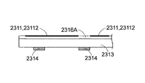
本発明の実施形態に係る発光キーボードについて、図5は本発明に係る発光キーボードの第1の好ましい実施形態における構造の側面図である。発光キーボード2は下から上に順番に台座22、薄膜回路基板23、キー底板29、及び複数のキー24を含む。発光キーボード2は更に、薄膜回路基板23の側辺に取り付けられて、薄膜回路基板23の方向に照射される発光素子21を含む。本実施形態では、発光素子21は発光ダイオードである。また、台座22は薄膜回路基板23、キー底板29、及び複数のキー24を載置するためのものである。
[First embodiment]
Regarding the light-emitting keyboard according to the embodiment of the present invention, FIG. 5 is a side view of the structure of the light-emitting keyboard according to the first preferred embodiment of the present invention. The
さらに、図6は図5に示された発光キーボードの薄膜回路基板の分解斜視図で、薄膜回路基板23は下層板231と上層板232を含む。下層板231の上表面には第1回路パターン2311があり、第1回路パターン2311上には複数の下接点23111を設け、上層板232には上層薄膜2322と、上層薄膜2322の下表面に形成された第2回路パターン2321があり、第2回路パターン2321上は複数の下接点23111に対応する複数の上接点23211があり、このうち、各上接点23211とこれに対応する下接点23111の間に間隔Dがあり、対応する下接点23111と共に薄膜スイッチ234を形成する。各上接点23211とこれに対応する下接点23111の間に間隔Dを設けるため、本実施形態では、薄膜回路基板23は更に、下層板231と上層板232の間に取り付けられた中層板233を含み、中層板233は複数の下接点23111と複数の上接点23211に対応する複数の孔2331を有する。
6 is an exploded perspective view of the thin film circuit board of the light emitting keyboard shown in FIG. 5. The thin
図5によれば、キー底板29は複数のキー24をその上に連接させて、複数のキー24に対応する複数の貫通孔291があり、複数のキー24は複数の薄膜スイッチ234に対応する箇所に取り付けられ、各キー24は何れもキーキャップ241と連接部材243を備え、連接部材243はキー底板29とキーキャップ241の間に取り付けられ、キー底板29とキーキャップ241に連接して、キーキャップ241がキー底板29に対向して上下移動できるようにする。
According to FIG. 5, the
本好ましい実施形態では、連接部材243は鋏型連接部材で、第1フレーム2431と第2フレーム2432を含む。キー底板29は更に第1固定構造292と第2固定構造293を備え、複数のキー24のうち各キー24は更に、キーキャップ241とキー底板29の間に取り付けられて当接部2421を有する弾性体242を備える。また、各キー24のキーキャップ241は何れも第1キーキャップ固定構造2411と第2キーキャップ固定構造2412を含む。
In the present preferred embodiment, the connecting
このうち、第1フレーム2431の一端2431Aは第2固定構造293に連接され、他端2431Bは第1キーキャップ固定構造2411に連接され、また、第2フレーム2432の一端2432Aは第1固定構造292に連接され、他端2432Bは第2キーキャップ固定構造2412に連接される。当然ながら、上記は一実施態様に過ぎず、これを以って本願に係る連接部材243、キー底板29、及びキーキャップ241間の連結関係を限定するものではない。
Among these, one
また、本好ましい実施形態では、何れかのキー24が押下されてキー底板29に対向して下に移動すると、連接部材243の第1フレーム2431と第2フレーム2432が開いた状態から折り畳まれた状態となり、下に移動するキーキャップ241が弾性体242を圧迫し、弾性体2422の当接部2421がキー底板29上の対応する貫通孔291を貫通して、これに対応する上接点23211に当接し、さらにこれに対応する上接点23211が対応する接点孔2331より対応する下接点23111に接触することで、対応する薄膜スイッチ234が電気的に導通されて、発光キーボード2が対応するキー信号を生じる。キー24がこれ以上押下されなくなると、キーキャップ241は弾性体242の弾性力によって、キー底板29に対向して上に移動し、このとき第1フレーム2431と第2フレーム2432は折り畳まれた状態から開いた状態となり、キーキャップ241は元の位置に戻る。
Further, in the present preferred embodiment, when any key 24 is pressed and moved downward against the
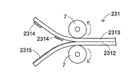
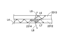
本願の発明特徴の一つは発光キーボード2における薄膜回路基板23の下層板231が複数層の薄膜設計であることである。図7は本発明に係る発光キーボードの第1の好ましい実施形態における薄膜回路基板の下層板の構造の側面図と工程概略図である。第1の好ましい実施形態では、下層板231は第2薄膜2312と、第2薄膜2312の上表面に接着された第1薄膜2313とを含み、第1薄膜2313と第2薄膜2312の間には、発光素子21から提供された光線を集光し乱反射するための複数の導光点2314があり、複数の導光点2314は複数のキー24の位置に応じて取り付けられて、光線を上向きに複数のキー24領域に投射することができる。また、第1薄膜2313と第2薄膜2312は導光薄膜で、その素材はポリカーボネート(PC)、又はポリエチレン(PET)等でよく、第1回路パターン2311は第1薄膜2313の上表面に印刷される。
One of the features of the invention of the present application is that the
下層板231の製造方法は次の通りである。先ず第1薄膜2313の下表面に複数の導光点2314を設け、第2薄膜2312の上表面に光線が透過できる透明の接着剤2315を付け、又は第2薄膜2312の上表面に複数の導光点2314を設け、第1薄膜2313の下表面に光線が透過できる透明の接着剤2315を付けた上で、ローラ7による熱圧着、又は冷圧着で、第1薄膜2313と第2薄膜2312を相互に貼り合せることができる。
The manufacturing method of the
図8は図7に示された下層板の光路の概略図である。図5によれば、発光素子21から提供された光線が下層板231に進入すると、光線L4は第2薄膜2312と第1薄膜2313内で拡散されて、光線が導光点2314に当たると、導光点2314は一部の光線を集光して、別の一分の光線を上向きと下向きに乱反射させる。このうち、上向きに乱反射した一部の光線L5は第1薄膜2313内を伝導し、別の一部の光線L6は第1薄膜2313とキー底板29上の対応する貫通孔291を順番に透過して上向きにキー24領域に投射されて、複数のキー24が発光効果を生じ、下向きに乱反射した一部の光線L7は第2薄膜2312内を伝導し、別の一部の光線L8は第2薄膜2312を透過して流失する。
FIG. 8 is a schematic view of the optical path of the lower layer plate shown in FIG. According to FIG. 5, when the light beam provided from the
第1好ましい実施形態における下層板の長所は次のとおりである。複数の導光点2314が第1薄膜2313と第2薄膜2312の間に設けられて、導光点2314から下向きに乱反射された光線の一部の光線L7(引き続き第2薄膜2312内を伝導する光線L7)は、第2薄膜2312で回收利用されるため、一部の光線L8(第2薄膜2312を透過する光線L8)しか流失を来たさない。即ち、下層板231に第1薄膜2313と複数の導光点2314しかなく、第2薄膜2312がなければ、導光点2314から下向きに乱反射された光線は完全に流失する。
Advantages of the lower layer plate in the first preferred embodiment are as follows. A plurality of
[第2実施形態]
次は、本発明の発光キーボードの第2実施形態について説明する。これは第1の好ましい実施形態とほぼ同じで、相違点は薄膜回路基板の下層板の組立構造にある。但し、下層板は複数層の薄膜設計のままである。図9、図10によれば、図9は本発明に係る発光キーボードの第2の好ましい実施形態における薄膜回路基板の下層板の構造の側面図で、図10は図9に示された下層板の別の視角からの構造の概略図である。
[Second Embodiment]
Next, a second embodiment of the light emitting keyboard of the present invention will be described. This is substantially the same as in the first preferred embodiment, and the difference is in the assembly structure of the lower layer plate of the thin film circuit board. However, the lower layer plate is still a multi-layer thin film design. 9 and 10, FIG. 9 is a side view of the structure of the lower layer plate of the thin film circuit board in the second preferred embodiment of the light emitting keyboard according to the present invention, and FIG. 10 is the lower layer plate shown in FIG. It is the schematic of the structure from another viewing angle.
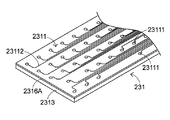
第2の好ましい実施形態では、下層板231は第1薄膜2313と第1薄膜2313の上表面に取り付けられた間隔薄膜2316Aとを含み、このうち、複数の導光点2314は第2薄膜2313の下表面に設けられ、複数のキー24の位置に応じて取り付けられて、複数の導光点2314が光線を上向きに複数のキー24領域に投射する。また、第1回路パターン2311は間隔薄膜2316Aの上表面に印刷され、第1回路パターン2311は複数の下接点23111と複数の金属回路23112で構成され、前記複数の金属回路23112は光線を集光し乱反射させる性質を持つ。本好ましい実施形態では、前記複数の金属回路23112は導電係数が良好な銀ペースト回路を採用し、間隔薄膜2316Aは単一の連続する薄膜で、前記複数の金属回路23112は単一の連続する薄膜上に形成される。
In the second preferred embodiment, the
また、下層板231の工程は、間隔薄膜2316Aは印刷工程、めっき皮膜工程、接着工程、または熱圧着工程で第1薄膜2313の上表面に形成される。なお、第1薄膜2313は導光薄膜で、その素材はポリカーボネート(PC)、ポリエチレン(PET)、又はポリメタクリル酸メチル樹脂(PMMA)素材等でよく、間隔薄膜2316の素材は第1薄膜2313と異なる。
In the process of the
図11は図9に示された下層板の光路の概略図である。発光素子21から提供された光線が下層板231に進入すると、光線L9は第1薄膜2313内で拡散され、光線L9が導光点2314に当たると、導光点2314は一部の光線を集光し、別の一部の光線を上向きに乱反射させる。このうち、上向きに乱反射した一部の光線L10は第1薄膜2313内を伝導し、別の一部の光線L11は第1薄膜2313を透過する。
FIG. 11 is a schematic view of the optical path of the lower layer plate shown in FIG. When the light beam provided from the
第2の好ましい実施形態では、間隔薄膜2316Aが第1回路パターン2311と第1薄膜2313の間にあり、しかもその素材が第1薄膜2313と異なるため、即ち、間隔薄膜2316の屈折率が第1薄膜2313の屈折率より小さいため、光線が第1薄膜2313内で全反射(例:光線L9、光線L10のコース)が起き易く、光線が第1薄膜2313を透過後に(例:光線L11のコース)、第1回路パターン2311の金属回路23112に集光されて乱反射されないようにする。このように、下層板231内の複数の導光点2314が上向きに乱反射する光量を増やして、発光キーボード2のキー24に更に多くの光量が得られる。また、前記複数個の導光点2314は本実施態様を限定するための必要部材ではない。続いて、本発明に係る発光キーボードにおける第3の好ましい実施形態を説明する。それは第2の好ましい実施形態とほぼ同じで、相違点は下層板の間隔薄膜の構造にあり、しかも薄膜回路基板には導光点が全くない。図12と図13によれば、図12は本発明に係る発光キーボードの第3の好ましい実施形態における薄膜回路基板の下層板の構造の側面図で、図13は図12に示された下層板の別の視角からの構造の概略図である。
In the second preferred embodiment, the gap
[第3の実施形態]
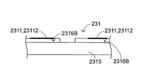
次は、本発明に係る発光キーボードの第3の実施形態について説明する。第3の好ましい実施形態では、下層板231の間隔薄膜2316Bは複数のブロックが分離されたブロック薄膜23161、23162、23163、23164で構成され、前記複数の金属回路23112はそれぞれ前記複数のブロック薄膜23161〜23164上に形成される。同様に、前記複数のブロック薄膜23161〜23164の屈折率は何れも第1薄膜2313の屈折率より小さい。当然ながら、上記は好ましい実施態様であり、当業者が実際の応用ニーズに応じて均等な変更設計を行なうことができ、例えば、一部の金属回路23112は複数のブロック薄膜23161〜23164のうちの何れか2つのブロック薄膜に跨いで形成されることが可能である。
[Third Embodiment]
Next, a third embodiment of the light-emitting keyboard according to the present invention will be described. In the third preferred embodiment, the gap
図14は図12に示された下層板の光路の概略図である。空気の屈折率は1であり、現行の技術では、空気の屈折率より小さい屈折率の材料は殆ど困難であるため、光線L9が下層板231の側辺から進入すると、第1薄膜2313上の間隔薄膜2316Bが取り付けられていない箇所が、光線L9が第1薄膜2313内で全反射を起こす効率がベストな箇所である旨先ず説明しておく。従って、本好ましい実施形態における光線L9が第1薄膜2313内で全反射する効率が第2の好ましい実施形態で述べたものよりさらに優れていることから、本好ましい実施形態では、下層板231に提供された光線を第1薄膜2313全体に更に均等に拡散させることができる。
FIG. 14 is a schematic view of the optical path of the lower layer plate shown in FIG. Since the refractive index of air is 1 and a material having a refractive index smaller than that of air is almost difficult with the current technology, when the light beam L9 enters from the side of the
[第4実施形態]
続いて、本発明に係る発光キーボードの第4の好ましい実施形態について説明する。それは第1と第2好ましい実施形態とほぼ同じで、相違点は薄膜回路基板23の下層板231の組立構造にあり、第4の好ましい実施形態の下層板231の組立構造は第1と第2好ましい実施形態における下層板を組合せた設計である。図15は本発明に係る発光キーボードの第4の好ましい実施形態における薄膜回路基板の下層板の構造の側面図である。
[Fourth Embodiment]
Next, a fourth preferred embodiment of the luminescent keyboard according to the present invention will be described. It is substantially the same as the first and second preferred embodiments, the difference being in the assembly structure of the
以下、図5で説明する。第4の好ましい実施形態では、下層板231は第2薄膜2312、第2薄膜2312の上表面に接着した第1薄膜2313、及び第1薄膜2313の上表面に取り付けられた間隔薄膜2316を含み、第1薄膜2313と第2薄膜2312の間は発光素子21から提供された光線を集光し乱反射するための複数の導光点2314があり、複数の導光点2314は複数のキー24の位置に応じて取り付けられ、複数の導光点2314から光線を上向きに投射して、キー底板29上の複数個の貫通孔291を貫通して複数のキー領域24に投射される。
This will be described below with reference to FIG. In a fourth preferred embodiment, the
また、第1回路パターン2311は間隔薄膜2316の上表面に印刷されて複数の金属回路23112を有し、前記金属回路23112は光線を集光して乱反射させる性質を持つ。このため、第4の好ましい実施形態における下層板231の長所は、第1と第2好ましい実施形態で述べた長所の組合せであり、また、第4の好ましい実施形態における下層板231の素材、工程は第1と第2の好ましい実施形態で述べたものと同じであるので、ここではこれ以上詳述しないこととする。また、前記複数個の導光点2314は本実施態様を限定するための必要部材ではない。当然ながら、当業者は上記第4の好ましい実施形態から得られた示唆で、第1と第3の好ましい実施形態における下層板の設計を組合せることができる。
The
[第5実施形態]
次は、本発明の発光キーボードの第5実施形態について説明する。図16は本発明に係る第5の好ましい実施形態の発光キーボードの構造の側面図で、図17は図16に示された発光キーボードの薄膜回路基板の構造の概略図である。第5の好ましい実施形態の発光キーボード3は第1好ましい実施形態とほぼ同じで、相違点は薄膜回路基板26が単一層の板構造であることにあり、薄膜回路基板26の上表面には回路パターン263を有し、回路パターン263には複数の薄膜スイッチ2631と金属回路2632があり、各薄膜スイッチ2631は第1導電部26311と第2導電部26312を含み、第1導電部26311は第2導電部26312に接触していない。
[Fifth Embodiment]
Next, a fifth embodiment of the light-emitting keyboard of the present invention will be described. 16 is a side view of the structure of the light-emitting keyboard according to the fifth preferred embodiment of the present invention. FIG. 17 is a schematic view of the structure of the thin-film circuit board of the light-emitting keyboard shown in FIG. The light-emitting
また、各キー25は更にキーキャップ251に連接された導体252を有し、導体252はキーキャップ251とキー底板29の間にある。キーキャップ251が押下されて、キー底板29に対向して下に移動すると、連接部材253の第1フレーム2531と第2フレーム2532は開いた状態から折り畳まれた状態となり、導体252はキー底板29上の対応する貫通孔291を貫通して、対応する薄膜スイッチ2631に接触することで、薄膜スイッチ2631が電気的に導通されて、発光キーボード3が対応するキー信号を生じる。
Each key 25 further has a
因みに、本実施形態における薄膜回路基板26は複数層の薄膜の設計のままであり、第1薄膜262と第2薄膜261(第1実施形態における第1薄膜2313と第2薄膜2312と同じ)を含み、第1薄膜262と第2薄膜261の間に同様に発光素子21から提供された光線を集光して乱反射するための複数の導光点2614があることから、本実施形態における薄膜回路基板26も第1の好ましい実施形態における下層板231と同様の長所を有する。
Incidentally, the thin
また、第6の好ましい実施形態では、第5の好ましい実施形態における発光キーボード3の薄膜回路基板26は第2の好ましい実施形態における下層板231の薄膜積層方式と同じでよく、第1薄膜262と、第1薄膜262の上表面に取り付けられた間隔薄膜(図示せず)とを含み、複数の導光点2614は第1薄膜262の下表面に取り付けられることから、薄膜回路基板26は第2の好ましい実施形態における下層板231と同じ長所を有する。
In the sixth preferred embodiment, the thin
また、第7の好ましい実施形態では、第5の好ましい実施形態における発光キーボード3の薄膜回路基板26は第3の好ましい実施形態における下層板231の薄膜積層方式と同じでよく、第1薄膜262と、第1薄膜262の上表面に取り付けられた間隔薄膜(図示せず)とを含み、間隔薄膜はブロックが分離した複数のブロック薄膜で構成されることから、薄膜回路基板26は第3の好ましい実施形態における下層板231と同じ長所を有する。
In the seventh preferred embodiment, the thin
また、第8実施形態では、第5の好ましい実施形態における発光キーボード3の薄膜回路基板26は第4の好ましい実施形態における下層板231の薄膜積層方式と同じでよく、第2薄膜261と、第2薄膜261の上表面に接着した第1薄膜262と、第1薄膜262の上表面に取り付けられた間隔薄膜(図示せず)とを含み、第1薄膜262と第2薄膜261の間には発光素子21から提供された光線を集光して乱反射させる複数の導光点2614があることから、薄膜回路基板26は第4の好ましい実施形態における下層板231と同じ長所がある。
In the eighth embodiment, the thin-
以上の各好ましい実施形態で述べたことから以下のことが分かる。本発明に係る発光キーボード2、3は導光板を余分に取り付ける必要がないため、製造コストが節減され、発光キーボード2、3内の薄膜回路基板23、26や下層板231が複数層の薄膜方法での設計により、回路パターン263の金属回路2632や第1回路パターン2311の金属回路23112が光線を集光する性質であるためにキー24、25に使用されるべき光量が無駄となるのを防止することができ、導光点2614、2314から下向きに乱反射して流失する光線を回收して、前記複数の導光点2614、2314から上向きに乱反射する光量を増加し、発光キーボード2の複数のキー24、25が一層多くの光量を獲得できることから、本発明に係る発光キーボード2、3は発光素子21から提供された光線を最も効率的に運用する。
The following can be understood from the description in each of the above preferred embodiments. Since the light-emitting
また、本願の別の発明特徴は次のとおりである。キー底板29が複数のキー24、25と薄膜回路基板23、26の間に取り付けられるため、薄膜回路基板23、26は特にホールを設ける必要なくして、各連接部材243を、対応するキー底板29と対応するキーキャップ241、251に連接することができる。従って、薄膜回路基板23、26にホールが無いことで、薄膜回路基板23、26の導光作用が連続される。即ち、発光素子26から提供された光線がホールに当たって前進が中断されることがないため、発光キーボード2、3の発光効率が一層大幅に向上される。
Further, another invention feature of the present application is as follows. Since the
上述の実施形態は本発明の技術思想及び特徴を説明するためのものにすぎず、当該技術分野を熟知する者に本発明の内容を理解させると共にこれをもって実施させることを目的とし、本発明の特許請求の範囲を限定するものではない。従って、本発明の精神を逸脱せずに行う各種の同様の効果をもつ改良又は変更は、後述の請求項に含まれるものとする。 The above-described embodiments are merely for explaining the technical idea and features of the present invention, and are intended to allow those skilled in the art to understand the contents of the present invention and to carry out the same with the present invention. It is not intended to limit the scope of the claims. Accordingly, improvements or modifications having various similar effects made without departing from the spirit of the present invention shall be included in the following claims.
1 発光キーボード
2 発光キーボード
4 発光キーボード
7 ローラ
9 発光キーボード
11 光反射板
12 導光板
13 キー底板
14 薄膜回路基板
15 キー
16 発光素子
21 発光素子
22 台座
23 薄膜回路基板
24 複数のキー
26 薄膜回路基板
29 キー底板
93 キー底板
94 薄膜回路基板
96 発光素子
121 導光点
131 貫通孔
132 第1固定構造
133 第2固定構造
141 下層板
142 上層板
143 中層板
144 薄膜スイッチ
145 ホール
146 ホール
151 キーキャップ
152 弾性体
153 鋏型連接部材
231 下層板
232 上層板
233 中層板
234 薄膜スイッチ
241 キーキャップ
242 弾性体
243 連接部材
251 キーキャップ
252 導体
253 連接部材
261 第2薄膜
262 第1薄膜
263 回路パターン
291 貫通孔
292 第1固定構造
293 第2固定構造
932 第1固定構造
933 第2固定構造
941 下層板
945 ホール
946 ホール
947 導光点
1411 第1回路パターン
1421 第2回路パターン
1431 接点孔
1511 第1キーキャップ固定構造
1512 第2キーキャップ固定構造
1531 第1フレーム
1531A 第1フレームの一端
1531B 第1フレームの他端
1532 第2フレーム
1532A 第2フレームの一端
1532B 第2フレームの他端
2311 第1回路パターン
2312 第2薄膜
2313 第1薄膜
2314 導光点
2315 透明の接着剤
2316A 間隔薄膜
2316B 間隔薄膜
2321 第2回路パターン
2322 上層薄膜
2331 孔
2411 第1キーキャップ固定構造
2412 第2キーキャップ固定構造
2421 当接部
2431 第1フレーム
2431A 第1フレームの一端
2431B 第1フレームの他端
2432 第2フレーム
2432A 第2フレームの一端
2432B 第2フレームの他端
2531 第1フレーム
2532 第2フレーム
2614 導光点
2631 薄膜スイッチ
2632 金属回路
14111 銀ペースト回路
14112 下接点
14211 銀ペースト回路
14212 上接点
23111 下接点
23112 金属回路
23211 上接点
23161 ブロック薄膜
23162 ブロック薄膜
23163 ブロック薄膜
23164 ブロック薄膜
26311 第1導電部
26312 第2導電接部
D 間隔
L1〜L11 光線
DESCRIPTION OF
1531A First end 1531B First frame
23161 Block
Claims (46)
薄膜回路基板と、
前記複数の薄膜スイッチに対応し導通するための複数のキーと、
前記複数のキーをその上に連接させ、前記複数のキーに対応する複数の貫通孔を有し、前記複数のキーと前記薄膜回路基板の間にあるキー底板と、
を含み、且つ前記薄膜回路基板は、
第1回路パターンと複数の導光点を有し、前記第1回路パターンには複数の下接点があり、前記複数の導光点は前記発光素子から提供された光線を集光して乱反射させ、前記複数の導光点が上向きに乱反射する光量を増加させるための第1薄膜と第2薄膜を含む下層板と、
第2回路パターンを有し、前記第2回路パターン上に前記複数の下接点に対応する複数の上接点があり、前記各上接点とこれに対応する前記下接点との間に間隔があり、前記対応する下接点と共に薄膜スイッチを形成する上層板と、
を含むことを特徴とする発光キーボード。 At least one light emitting element for providing light to the light emitting keyboard;
A thin film circuit board;
A plurality of keys for conducting in correspondence with the plurality of thin film switches;
A plurality of through holes corresponding to the plurality of keys, the key bottom plate being located between the plurality of keys and the thin film circuit board;
And the thin film circuit board comprises:
The first circuit pattern has a plurality of light guide points, the first circuit pattern has a plurality of bottom contacts, and the light guide points collect and diffusely reflect the light beam provided from the light emitting element. A lower layer plate including a first thin film and a second thin film for increasing the amount of light that the plurality of light guide points diffusely reflect upward,
A plurality of upper contacts corresponding to the plurality of lower contacts on the second circuit pattern, and there is an interval between each upper contact and the corresponding lower contact; An upper plate forming a thin film switch with the corresponding lower contact;
A luminescent keyboard comprising:
前記発光キーボードの外部に露出したキーキャップと、
前記キー底板と前記キーキャップの間に取り付けられ、前記キー底板と前記キーキャップを連接して、前記キーキャップを前記キー底板に対向して上下移動させる連接部材と、
を含むことを特徴とする請求項1に記載の発光キーボード。 Each key is
A keycap exposed to the outside of the luminous keyboard;
A connecting member attached between the key bottom plate and the key cap, connecting the key bottom plate and the key cap, and moving the key cap up and down facing the key bottom plate;
The light-emitting keyboard according to claim 1, comprising:
回路パターンと複数の導光点を有し、前記回路パターンには複数の薄膜スイッチがあり、前記複数の導光点は前記発光素子から提供された光線を集光して乱反射させ、前記複数の導光点が上向きに乱反射する光量を増加させるための第1薄膜と第2薄膜を含む薄膜回路基板と、
前記複数の薄膜スイッチに対応し導通するための複数のキーと、
前記複数のキーをその上に連接させ、前記複数のキーに対応する複数の貫通孔を有し、前記複数のキーと前記薄膜回路基板の間にあるキー底板と、
を含むことを特徴とする発光キーボード。 At least one light emitting element for providing light to the light emitting keyboard;
The circuit pattern has a plurality of light guide points, the circuit pattern has a plurality of thin film switches, and the light guide points collect and diffusely reflect the light beam provided from the light emitting element. A thin film circuit board including a first thin film and a second thin film for increasing the amount of light that is diffusely reflected by the light guide point upward;
A plurality of keys for conducting in correspondence with the plurality of thin film switches;
A plurality of through holes corresponding to the plurality of keys, the key bottom plate being located between the plurality of keys and the thin film circuit board;
A luminescent keyboard comprising:
前記発光キーボードの外部に露出したキーキャップと、
前記キー底板と前記キーキャップの間に取り付けられ、前記キー底板と前記キーキャップを連接して、前記キーキャップを前記キー底板に対向して上下移動させる連接部材と、
前記キーキャップと前記キー底板の間に取り付けられた導体と、
を含み、前記キーキャップが押下されると、前記導体が前記キー底板の対応する前記貫通孔を貫通して、対応する前記薄膜スイッチに接触して前記薄膜スイッチを導通することを特徴とする請求項18に記載の発光キーボード。 Each key is
A keycap exposed to the outside of the luminous keyboard;
A connecting member attached between the key bottom plate and the key cap, connecting the key bottom plate and the key cap, and moving the key cap up and down facing the key bottom plate;
A conductor attached between the key cap and the key bottom plate;
And when the key cap is depressed, the conductor passes through the corresponding through hole of the key bottom plate, contacts the corresponding thin film switch, and conducts the thin film switch. Item 19. A light emitting keyboard according to Item 18.
薄膜回路基板と、
前記複数の薄膜スイッチを導通するための複数のキーと、
前記複数のキーをその上に連接させ、前記複数のキーに対応する複数の貫通孔を有し、前記複数のキーと前記薄膜回路基板の間にあるキー底板と、
を含み、且つ前記薄膜回路基板は、
上層薄膜と前記上層薄膜の下表面に形成された第2回路パターンを有し、前記第2回路パターン上に複数の上接点を設けた上層板と、
第1薄膜、第2回路パターン、及び前記第1薄膜と前記第1回路パターンの間にある第2薄膜を有し、前記第1回路パターン上に前記複数の上接点に対応する複数の下接点を設け、前記各上接点とこれに対応する前記下接点の間に間隔があり、前記対応する上接点と共に薄膜スイッチを形成し、前記第2薄膜の屈折率が前記第1薄膜の屈折率より小さい下層板と、
を含むことを特徴とする発光キーボード。 At least one light emitting element for providing light to the light emitting keyboard;
A thin film circuit board;
A plurality of keys for conducting the plurality of thin film switches;
A plurality of through holes corresponding to the plurality of keys, the key bottom plate being located between the plurality of keys and the thin film circuit board;
And the thin film circuit board comprises:
An upper layer board having a second circuit pattern formed on the lower surface of the upper layer thin film and the upper layer thin film, and provided with a plurality of upper contacts on the second circuit pattern;
A plurality of lower contacts corresponding to the plurality of upper contacts on the first circuit pattern, the first thin film, the second circuit pattern, and a second thin film between the first thin film and the first circuit pattern A gap is formed between each upper contact and the corresponding lower contact, and a thin film switch is formed together with the corresponding upper contact. The refractive index of the second thin film is higher than the refractive index of the first thin film. A small underlayer,
A luminescent keyboard comprising:
前記発光キーボードの外部に露出したキーキャップと、
前記キー底板と前記キーキャップの間に取り付けられ、前記キー底板と前記キーキャップを連接して、前記キーキャップを前記キー底板に対向して上下移動させる連接部材と、
を含むことを特徴とする請求項33に記載の発光キーボード。 Each key is
A keycap exposed to the outside of the luminous keyboard;
A connecting member attached between the key bottom plate and the key cap, connecting the key bottom plate and the key cap, and moving the key cap up and down facing the key bottom plate;
The light-emitting keyboard according to claim 33, comprising:
Applications Claiming Priority (2)
| Application Number | Priority Date | Filing Date | Title |
|---|---|---|---|
| TW100143439A TWI459424B (en) | 2011-11-25 | 2011-11-25 | Luminous keyboard |
| TW100143439 | 2011-11-25 |
Related Child Applications (1)
| Application Number | Title | Priority Date | Filing Date |
|---|---|---|---|
| JP2016174158A Division JP2016201377A (en) | 2011-11-25 | 2016-09-07 | Luminous keyboard |
Publications (2)
| Publication Number | Publication Date |
|---|---|
| JP2013115035A true JP2013115035A (en) | 2013-06-10 |
| JP2013115035A5 JP2013115035A5 (en) | 2015-02-05 |
Family
ID=48465818
Family Applications (2)
| Application Number | Title | Priority Date | Filing Date |
|---|---|---|---|
| JP2011280053A Pending JP2013115035A (en) | 2011-11-25 | 2011-12-21 | Luminous keyboard |
| JP2016174158A Pending JP2016201377A (en) | 2011-11-25 | 2016-09-07 | Luminous keyboard |
Family Applications After (1)
| Application Number | Title | Priority Date | Filing Date |
|---|---|---|---|
| JP2016174158A Pending JP2016201377A (en) | 2011-11-25 | 2016-09-07 | Luminous keyboard |
Country Status (3)
| Country | Link |
|---|---|
| US (1) | US8878086B2 (en) |
| JP (2) | JP2013115035A (en) |
| TW (1) | TWI459424B (en) |
Families Citing this family (17)
| Publication number | Priority date | Publication date | Assignee | Title |
|---|---|---|---|---|
| TWI459425B (en) * | 2012-12-19 | 2014-11-01 | Primax Electronics Ltd | Illuminating keyboard |
| TWI539328B (en) * | 2013-07-19 | 2016-06-21 | 致伸科技股份有限公司 | Luminous keyboard and light guide plate module thereof |
| CN104347299B (en) * | 2013-08-05 | 2017-04-12 | 致伸科技股份有限公司 | Light emitting keyboard and light guide plate module thereof |
| CN104347298A (en) * | 2013-08-05 | 2015-02-11 | 致伸科技股份有限公司 | Light emitting keyboard |
| US20160109636A1 (en) * | 2014-10-16 | 2016-04-21 | Chicony Electronics Co., Ltd. | Backlight module capable of avoiding light leakage |
| CN104992869B (en) * | 2015-07-15 | 2016-05-11 | 苏州达方电子有限公司 | Backlight module and the keyboard that comprises it |
| TWI563528B (en) * | 2015-09-30 | 2016-12-21 | Giga Byte Tech Co Ltd | Keystroke logging device and light guide element |
| TWI601178B (en) * | 2016-12-14 | 2017-10-01 | 致伸科技股份有限公司 | Illumanating keyboard |
| TW201830443A (en) * | 2017-02-10 | 2018-08-16 | 致伸科技股份有限公司 | Keyboard device |
| TW201916085A (en) * | 2017-10-13 | 2019-04-16 | 致伸科技股份有限公司 | Luminous keyboard |
| CN110208899B (en) * | 2018-08-01 | 2021-02-26 | 光宝电子(广州)有限公司 | Backlight module and input device |
| CN109887789A (en) * | 2019-01-29 | 2019-06-14 | 苏州达方电子有限公司 | Luminous button and illuminated keyboard comprising the luminous button |
| US10991524B2 (en) * | 2019-04-10 | 2021-04-27 | Dell Products L.P. | Information handling system keyboard discrete row illumination |
| CN211604989U (en) * | 2019-06-17 | 2020-09-29 | 光宝电子(广州)有限公司 | Backlight module and keyboard using same |
| CN111477487B (en) | 2019-06-18 | 2023-07-14 | 光宝电子(广州)有限公司 | Input device |
| CN112449490B (en) * | 2019-08-30 | 2022-04-01 | 致伸科技股份有限公司 | Thin film circuit structure |
| TWI696203B (en) * | 2019-10-25 | 2020-06-11 | 致伸科技股份有限公司 | Keyboard structure |
Citations (7)
| Publication number | Priority date | Publication date | Assignee | Title |
|---|---|---|---|---|
| JPH01272003A (en) * | 1988-04-21 | 1989-10-31 | Fujitsu Ltd | Light conducting panel |
| JP2006318905A (en) * | 2005-05-13 | 2006-11-24 | Samsung Electronics Co Ltd | Keypad having light guide layer, keypad assembly, and portable terminal |
| US20070257822A1 (en) * | 2006-03-28 | 2007-11-08 | Joo-Hoon Lee | Keypad assembly |
| JP2007535790A (en) * | 2004-04-30 | 2007-12-06 | オイ モディリス リミテッド | Ultra thin lighting element |
| JP2009043471A (en) * | 2007-08-07 | 2009-02-26 | Citizen Electronics Co Ltd | Light guide plate, planar light unit, and display device |
| JP2009123183A (en) * | 2007-11-15 | 2009-06-04 | Lite-On Technology Corp | Keyboard with backlight |
| WO2010046694A1 (en) * | 2008-10-21 | 2010-04-29 | Iti Scotland Limited | Light guides |
Family Cites Families (10)
| Publication number | Priority date | Publication date | Assignee | Title |
|---|---|---|---|---|
| US6861600B1 (en) * | 2003-10-01 | 2005-03-01 | Lumitex, Inc. | Integrated switch and backlight assembly |
| JP2008234863A (en) * | 2007-03-16 | 2008-10-02 | Shin Etsu Polymer Co Ltd | Illuminating sheet structure and operation switch |
| TWI402717B (en) * | 2008-05-13 | 2013-07-21 | Chicony Electronic Co Ltd | Glowing keyboard |
| TWM352722U (en) * | 2008-10-22 | 2009-03-11 | Changshu Sunrex Technology Corp | Keyboard device capable of illuminating |
| US7952043B2 (en) * | 2008-12-11 | 2011-05-31 | Changshu Sunrex Technology Co., Ltd. | Keyboard with backlighting functionality |
| JP2011003371A (en) * | 2009-06-18 | 2011-01-06 | Panasonic Corp | Light guide sheet, and movable contact assembly using the same |
| TWI399776B (en) * | 2010-01-08 | 2013-06-21 | Zippy Tech Corp | Thin light-emitting keyboard |
| TW201140634A (en) * | 2010-05-07 | 2011-11-16 | Primax Electronics Ltd | Luminous keyboard |
| CN201773867U (en) * | 2010-07-12 | 2011-03-23 | 国基电子(上海)有限公司 | Structure of multi-layer staggered spot-distribution light guide element |
| TWI449071B (en) * | 2012-04-27 | 2014-08-11 | Primax Electronics Ltd | Luminous keying module of handheld device |
-
2011
- 2011-11-25 TW TW100143439A patent/TWI459424B/en not_active IP Right Cessation
- 2011-12-21 JP JP2011280053A patent/JP2013115035A/en active Pending
-
2012
- 2012-03-09 US US13/416,868 patent/US8878086B2/en active Active
-
2016
- 2016-09-07 JP JP2016174158A patent/JP2016201377A/en active Pending
Patent Citations (7)
| Publication number | Priority date | Publication date | Assignee | Title |
|---|---|---|---|---|
| JPH01272003A (en) * | 1988-04-21 | 1989-10-31 | Fujitsu Ltd | Light conducting panel |
| JP2007535790A (en) * | 2004-04-30 | 2007-12-06 | オイ モディリス リミテッド | Ultra thin lighting element |
| JP2006318905A (en) * | 2005-05-13 | 2006-11-24 | Samsung Electronics Co Ltd | Keypad having light guide layer, keypad assembly, and portable terminal |
| US20070257822A1 (en) * | 2006-03-28 | 2007-11-08 | Joo-Hoon Lee | Keypad assembly |
| JP2009043471A (en) * | 2007-08-07 | 2009-02-26 | Citizen Electronics Co Ltd | Light guide plate, planar light unit, and display device |
| JP2009123183A (en) * | 2007-11-15 | 2009-06-04 | Lite-On Technology Corp | Keyboard with backlight |
| WO2010046694A1 (en) * | 2008-10-21 | 2010-04-29 | Iti Scotland Limited | Light guides |
Also Published As
| Publication number | Publication date |
|---|---|
| TW201322296A (en) | 2013-06-01 |
| US8878086B2 (en) | 2014-11-04 |
| TWI459424B (en) | 2014-11-01 |
| US20130134021A1 (en) | 2013-05-30 |
| JP2016201377A (en) | 2016-12-01 |
Similar Documents
| Publication | Publication Date | Title |
|---|---|---|
| JP2016201377A (en) | Luminous keyboard | |
| US8530768B2 (en) | Thin illuminated keyboard | |
| JP4279347B2 (en) | Light guide film and light emitting keypad provided with the same | |
| CN103839722B (en) | Illuminated keyboard | |
| CN103839715B (en) | Illuminated keyboard | |
| TWI539328B (en) | Luminous keyboard and light guide plate module thereof | |
| TWI423289B (en) | Membrane circuit board and luminous keyboard using the same | |
| TWI430310B (en) | Luminous keyboard | |
| TW201403646A (en) | Light emitting keyboard with light passage | |
| JP2013115035A5 (en) | ||
| CN102334328A (en) | Light diffuser actuator film (ldaf) keypad module | |
| JP2010244508A (en) | Light emitting keyboard | |
| US7897889B2 (en) | Movable contact element and switch using the same | |
| TWI449071B (en) | Luminous keying module of handheld device | |
| JP4398711B2 (en) | Illuminated keypad and illumination structure | |
| CN102253720A (en) | Luminescent keyboard | |
| CN102543539B (en) | Luminous keyboard | |
| CN203966910U (en) | Thin luminous keyboard | |
| TW201030788A (en) | Keyboard device | |
| TWM461863U (en) | Keyboard | |
| TWM446365U (en) | Luminous keyboard with luminous light bar | |
| TW201136288A (en) | Keypad | |
| JP2010186610A (en) | Key module and electronic device | |
| CN103390521A (en) | Light-emitting key module of handheld device | |
| TW201128452A (en) | Keyboard |
Legal Events
| Date | Code | Title | Description |
|---|---|---|---|
| A521 | Request for written amendment filed |
Free format text: JAPANESE INTERMEDIATE CODE: A523 Effective date: 20141216 |
|
| A621 | Written request for application examination |
Free format text: JAPANESE INTERMEDIATE CODE: A621 Effective date: 20141216 |
|
| A977 | Report on retrieval |
Free format text: JAPANESE INTERMEDIATE CODE: A971007 Effective date: 20150930 |
|
| A131 | Notification of reasons for refusal |
Free format text: JAPANESE INTERMEDIATE CODE: A131 Effective date: 20151006 |
|
| A521 | Request for written amendment filed |
Free format text: JAPANESE INTERMEDIATE CODE: A523 Effective date: 20151228 |
|
| A02 | Decision of refusal |
Free format text: JAPANESE INTERMEDIATE CODE: A02 Effective date: 20160517 |