JP2013104912A - Display device and display method - Google Patents
Display device and display method Download PDFInfo
- Publication number
- JP2013104912A JP2013104912A JP2011246770A JP2011246770A JP2013104912A JP 2013104912 A JP2013104912 A JP 2013104912A JP 2011246770 A JP2011246770 A JP 2011246770A JP 2011246770 A JP2011246770 A JP 2011246770A JP 2013104912 A JP2013104912 A JP 2013104912A
- Authority
- JP
- Japan
- Prior art keywords
- display
- peak level
- unit
- video signal
- partial
- Prior art date
- Legal status (The legal status is an assumption and is not a legal conclusion. Google has not performed a legal analysis and makes no representation as to the accuracy of the status listed.)
- Abandoned
Links
Images


Classifications
-
- G—PHYSICS
- G09—EDUCATION; CRYPTOGRAPHY; DISPLAY; ADVERTISING; SEALS
- G09G—ARRANGEMENTS OR CIRCUITS FOR CONTROL OF INDICATING DEVICES USING STATIC MEANS TO PRESENT VARIABLE INFORMATION
- G09G3/00—Control arrangements or circuits, of interest only in connection with visual indicators other than cathode-ray tubes
- G09G3/20—Control arrangements or circuits, of interest only in connection with visual indicators other than cathode-ray tubes for presentation of an assembly of a number of characters, e.g. a page, by composing the assembly by combination of individual elements arranged in a matrix no fixed position being assigned to or needed to be assigned to the individual characters or partial characters
- G09G3/34—Control arrangements or circuits, of interest only in connection with visual indicators other than cathode-ray tubes for presentation of an assembly of a number of characters, e.g. a page, by composing the assembly by combination of individual elements arranged in a matrix no fixed position being assigned to or needed to be assigned to the individual characters or partial characters by control of light from an independent source
- G09G3/3406—Control of illumination source
- G09G3/342—Control of illumination source using several illumination sources separately controlled corresponding to different display panel areas, e.g. along one dimension such as lines
- G09G3/3426—Control of illumination source using several illumination sources separately controlled corresponding to different display panel areas, e.g. along one dimension such as lines the different display panel areas being distributed in two dimensions, e.g. matrix
-
- G—PHYSICS
- G09—EDUCATION; CRYPTOGRAPHY; DISPLAY; ADVERTISING; SEALS
- G09G—ARRANGEMENTS OR CIRCUITS FOR CONTROL OF INDICATING DEVICES USING STATIC MEANS TO PRESENT VARIABLE INFORMATION
- G09G3/00—Control arrangements or circuits, of interest only in connection with visual indicators other than cathode-ray tubes
- G09G3/20—Control arrangements or circuits, of interest only in connection with visual indicators other than cathode-ray tubes for presentation of an assembly of a number of characters, e.g. a page, by composing the assembly by combination of individual elements arranged in a matrix no fixed position being assigned to or needed to be assigned to the individual characters or partial characters
- G09G3/34—Control arrangements or circuits, of interest only in connection with visual indicators other than cathode-ray tubes for presentation of an assembly of a number of characters, e.g. a page, by composing the assembly by combination of individual elements arranged in a matrix no fixed position being assigned to or needed to be assigned to the individual characters or partial characters by control of light from an independent source
- G09G3/36—Control arrangements or circuits, of interest only in connection with visual indicators other than cathode-ray tubes for presentation of an assembly of a number of characters, e.g. a page, by composing the assembly by combination of individual elements arranged in a matrix no fixed position being assigned to or needed to be assigned to the individual characters or partial characters by control of light from an independent source using liquid crystals
-
- G—PHYSICS
- G09—EDUCATION; CRYPTOGRAPHY; DISPLAY; ADVERTISING; SEALS
- G09G—ARRANGEMENTS OR CIRCUITS FOR CONTROL OF INDICATING DEVICES USING STATIC MEANS TO PRESENT VARIABLE INFORMATION
- G09G2320/00—Control of display operating conditions
- G09G2320/02—Improving the quality of display appearance
- G09G2320/0271—Adjustment of the gradation levels within the range of the gradation scale, e.g. by redistribution or clipping
-
- G—PHYSICS
- G09—EDUCATION; CRYPTOGRAPHY; DISPLAY; ADVERTISING; SEALS
- G09G—ARRANGEMENTS OR CIRCUITS FOR CONTROL OF INDICATING DEVICES USING STATIC MEANS TO PRESENT VARIABLE INFORMATION
- G09G2320/00—Control of display operating conditions
- G09G2320/02—Improving the quality of display appearance
- G09G2320/0285—Improving the quality of display appearance using tables for spatial correction of display data
-
- G—PHYSICS
- G09—EDUCATION; CRYPTOGRAPHY; DISPLAY; ADVERTISING; SEALS
- G09G—ARRANGEMENTS OR CIRCUITS FOR CONTROL OF INDICATING DEVICES USING STATIC MEANS TO PRESENT VARIABLE INFORMATION
- G09G2320/00—Control of display operating conditions
- G09G2320/06—Adjustment of display parameters
- G09G2320/0613—The adjustment depending on the type of the information to be displayed
- G09G2320/062—Adjustment of illumination source parameters
-
- G—PHYSICS
- G09—EDUCATION; CRYPTOGRAPHY; DISPLAY; ADVERTISING; SEALS
- G09G—ARRANGEMENTS OR CIRCUITS FOR CONTROL OF INDICATING DEVICES USING STATIC MEANS TO PRESENT VARIABLE INFORMATION
- G09G2320/00—Control of display operating conditions
- G09G2320/06—Adjustment of display parameters
- G09G2320/0626—Adjustment of display parameters for control of overall brightness
- G09G2320/0646—Modulation of illumination source brightness and image signal correlated to each other
Abstract
Description
本開示は、液晶表示素子を有する表示装置、およびその表示方法に関する。 The present disclosure relates to a display device having a liquid crystal display element and a display method thereof.
近年、表示装置においては、CRT(Cathode Ray Tube)から液晶表示装置などの薄型表示装置への移行が進んでいる。特に液晶表示装置は、低消費電力が実現できることから、薄型表示装置の主流になりつつなる。 In recent years, in display devices, a shift from a CRT (Cathode Ray Tube) to a thin display device such as a liquid crystal display device is progressing. In particular, liquid crystal display devices are becoming mainstream of thin display devices because they can realize low power consumption.
液晶表示装置については、さらなる消費電力の低減を目的としたいくつかの技術が提案されている。例えば、特許文献1,2には、バックライトを複数の領域に分割し、映像信号の輝度情報に応じて、その領域ごとにバックライトの発光輝度を独立して制御(部分駆動)する表示装置が開示されている。
As for liquid crystal display devices, several techniques for further reducing power consumption have been proposed. For example,
近年、エコロジーが注目を集めており、液晶表示装置では、さらなる消費電力の低減が望まれている。 In recent years, ecology has attracted attention, and liquid crystal display devices are desired to further reduce power consumption.
本開示はかかる問題点に鑑みてなされたもので、その目的は、消費電力を低減することができる表示装置および表示方法を提供することにある。 The present disclosure has been made in view of such a problem, and an object thereof is to provide a display device and a display method capable of reducing power consumption.
本開示の第1の表示装置は、液晶表示部と、バックライトと、処理部とを備えている。液晶表示部は、映像信号に基づいて画像を表示するものである。処理部は、表示画面またはその表示画面を区分してなる複数の部分表示領域のそれぞれにおける映像信号のピークレベルと、表示画面上の参照位置と係数データとを関連づけて構成されたデータマップから取得した係数データとに基づいて、映像信号を補正するとともに、バックライトの輝度を設定するものである。 The first display device according to the present disclosure includes a liquid crystal display unit, a backlight, and a processing unit. The liquid crystal display unit displays an image based on the video signal. The processing unit is obtained from a data map configured by associating a peak level of a video signal in each of a display screen or a plurality of partial display areas obtained by dividing the display screen, a reference position on the display screen, and coefficient data. Based on the obtained coefficient data, the video signal is corrected and the luminance of the backlight is set.
本開示の第2の表示装置は、液晶表示部と、バックライトと、処理部とを備えている。液晶表示部は、映像信号に基づいて画像を表示するものである。処理部は、表示画面またはその表示画面を区分してなる複数の部分表示領域のそれぞれにおける映像信号のピークレベルと、そのピークレベルが生じる表示画面上の位置であるピーク位置とに基づいて、映像信号を補正するとともに、バックライトの輝度を設定するものである。 The second display device according to the present disclosure includes a liquid crystal display unit, a backlight, and a processing unit. The liquid crystal display unit displays an image based on the video signal. Based on the peak level of the video signal in each of the display screen or a plurality of partial display areas obtained by dividing the display screen and the peak position that is the position on the display screen where the peak level occurs, While correcting the signal, the brightness of the backlight is set.
本開示の第3の表示装置は、液晶表示部と、バックライトと、処理部とを備えている。液晶表示部は、映像信号に基づいて画像を表示するものである。バックライトは、複数の部分発光部を有するものである。処理部は、各部分発光部に対応する部分表示領域における映像信号のピークレベルと、その部分表示領域の位置とに基づいて、映像信号を補正するとともに、部分発光部の輝度を設定するものである。 The third display device according to the present disclosure includes a liquid crystal display unit, a backlight, and a processing unit. The liquid crystal display unit displays an image based on the video signal. The backlight has a plurality of partial light emitting units. The processing unit corrects the video signal and sets the luminance of the partial light emitting unit based on the peak level of the video signal in the partial display region corresponding to each partial light emitting unit and the position of the partial display region. is there.
本開示の表示方法は、表示画面またはその表示画面を区分してなる複数の部分表示領域のそれぞれにおける映像信号のピークレベルと、表示画面上の位置と係数データとを関連づけて構成されたデータマップから取得した係数データとに基づいて、映像信号を補正するとともに、バックライトの輝度を設定し、補正された映像信号に基づいて画像を表示するものである。 The display method of the present disclosure is a data map configured by associating a peak level of a video signal in each of a display screen or a plurality of partial display areas obtained by dividing the display screen, a position on the display screen, and coefficient data. The video signal is corrected based on the coefficient data acquired from the above, the luminance of the backlight is set, and an image is displayed based on the corrected video signal.
本開示の第1の表示装置および表示方法では、映像信号に基づいて、液晶表示部において表示が行われる。その際、ピークレベルと、データマップから取得した係数データとに基づいて、映像信号が補正されるとともに、バックライトの輝度が設定され、その補正された映像信号に基づいて表示が行われる。 In the first display device and display method of the present disclosure, display is performed in the liquid crystal display unit based on the video signal. At that time, the video signal is corrected based on the peak level and the coefficient data acquired from the data map, the luminance of the backlight is set, and display is performed based on the corrected video signal.
本開示の第2の表示装置では、映像信号に基づいて、液晶表示部において表示が行われる。その際、ピークレベルとピーク位置とに基づいて、映像信号が補正されるとともに、バックライトの輝度が設定され、その補正された映像信号に基づいて表示が行われる。 In the second display device of the present disclosure, display is performed in the liquid crystal display unit based on the video signal. At that time, the video signal is corrected based on the peak level and the peak position, the luminance of the backlight is set, and display is performed based on the corrected video signal.
本開示の第3の表示装置では、映像信号に基づいて、液晶表示部において表示が行われる。その際、ピークレベルと部分表示領域の位置とに基づいて、映像信号が補正されるとともに、その部分表示領域に対応する部分発光部の輝度が設定され、その補正された映像信号に基づいて表示が行われる。 In the third display device of the present disclosure, display is performed in the liquid crystal display unit based on the video signal. At that time, the video signal is corrected based on the peak level and the position of the partial display area, and the luminance of the partial light emitting unit corresponding to the partial display area is set, and the display is performed based on the corrected video signal. Is done.
本開示の第1の表示装置および表示方法によれば、ピークレベル、およびデータマップから取得した係数データに基づいて、映像信号を補正するとともに、バックライトの輝度を設定したので、消費電力を低減することができる。 According to the first display device and display method of the present disclosure, the video signal is corrected and the luminance of the backlight is set based on the peak level and the coefficient data acquired from the data map, thereby reducing power consumption. can do.
本開示の第2の表示装置によれば、ピークレベルおよびピーク位置に基づいて、映像信号を補正するとともに、バックライトの輝度を設定したので、消費電力を低減することができる。 According to the second display device of the present disclosure, since the video signal is corrected and the luminance of the backlight is set based on the peak level and the peak position, power consumption can be reduced.
本開示の第3の表示装置によれば、ピークレベルおよび部分表示領域の位置に基づいて、映像信号を補正するとともに、部分発光部の輝度を設定したので、消費電力を低減することができる。 According to the third display device of the present disclosure, the video signal is corrected based on the peak level and the position of the partial display area, and the luminance of the partial light emitting unit is set, so that power consumption can be reduced.
以下、本開示の実施の形態について、図面を参照して詳細に説明する。なお、説明は以下の順序で行う。
1.第1の実施の形態
2.第2の実施の形態
3.第3の実施の形態
Hereinafter, embodiments of the present disclosure will be described in detail with reference to the drawings. The description will be given in the following order.
1.
<1.第1の実施の形態>
[構成例]
(全体構成例)
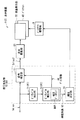
図1は、第1の実施の形態に係る表示装置の一構成例を表すものである。表示装置1は、バックライトを有する透過型の液晶表示装置である。なお、本開示の実施の形態に係る表示方法は、本実施の形態により具現化されるので、併せて説明する。
<1. First Embodiment>
[Configuration example]
(Overall configuration example)
FIG. 1 illustrates a configuration example of a display device according to the first embodiment. The
表示装置1は、信号処理部10と、表示駆動部20と、液晶表示部30と、バックライト駆動部9と、バックライト40とを備えている。
The
信号処理部10は、映像信号Sdispに基づいて、映像信号Sdisp2を生成するとともに、バックライト40の輝度を設定するものである。詳細については後述する。
The signal processing unit 10 generates the video signal Sdisp2 based on the video signal Sdisp and sets the luminance of the
表示駆動部20は、信号処理部10から供給される映像信号Sdisp2に基づいて、液晶表示部30を駆動するものである。液晶表示部30は、液晶表示素子により構成された表示部であり、バックライト40から射出した光を変調することにより表示を行うようになっている。
The
図2は、表示駆動部20および液晶表示部30のブロック図の一例を表すものである。 表示駆動部20は、タイミング制御部21と、ゲートドライバ22と、データドライバ23とを備えている。タイミング制御部21は、ゲートドライバ22およびデータドライバ23の駆動タイミングを制御するとともに、制御部11から供給された映像信号Sdisp2を映像信号Sdisp3としてデータドライバ23へ供給するものである。ゲートドライバ22は、タイミング制御部21によるタイミング制御に従って、液晶表示部30内の画素Pixを行ごとに順次選択して、線順次走査するものである。データドライバ23は、液晶表示部30の各画素Pixへ、映像信号Sdisp3に基づく画素信号を供給するものである。具体的には、データドライバ23は、映像信号Sdisp3に基づいてD/A(デジタル/アナログ)変換を行うことにより、アナログ信号である画素信号を生成し、各画素Pixへ供給するようになっている。
FIG. 2 illustrates an example of a block diagram of the
液晶表示部30は、例えばガラスなどから構成される2枚の透明基板の間に液晶材料を封入したものである。これらの透明基板の液晶材料に面した部分には、例えばITO(Indium Tin Oxide)などから構成される透明電極が形成され、液晶材料とともに画素Pixを構成している。
The liquid
図3は、液晶表示部30の回路図の一例を表すものである。液晶表示部30は、マトリックス状に配列した複数の画素Pixを有している。各画素Pixは、3つ(赤色、緑色、青色)のサブ画素SPixにより構成される。サブ画素SPixは、TFT素子Trおよび液晶素子LCを有している。TFT素子Trは、薄膜トランジスタにより構成されるものであり、この例では、nチャネルのMOS(Metal Oxide Semiconductor)型のTFTで構成されている。TFT素子Trのソースはデータ線SGLに接続され、ゲートはゲート線GCLに接続され、ドレインは液晶素子LCの一端に接続されている。液晶素子LCは、一端がTFT素子Trのドレインに接続され、他端は接地されている。ゲート線GCLはゲートドライバ22に接続され、データ線SGLはデータドライバ23に接続されている。
FIG. 3 illustrates an example of a circuit diagram of the liquid
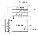
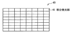
バックライト40は、バックライト駆動部14から供給される駆動信号に基づいて発光し、液晶表示部30に対してその光を射出するものである。
The
図4は、バックライト40の一構成例を表すものである。バックライト40は、いわゆる直下型方式のバックライトであり、マトリックス状に配列した複数の部分発光部41を有している。部分発光部41は、この例では、LED(Light Emitting Diode)を用いて構成されている。なお、これに限定されるものではなく、例えばCCFL(Cold Cathode Fluorescent Lamp)により構成してもよい。部分発光部41は、それぞれ設定された輝度で、独立して発光することができる。部分発光部41から射出した光は、主に液晶表示部30における対応する領域(後述する部分表示領域31)を透過して、表示装置1から射出するようになっている。
FIG. 4 shows a configuration example of the
(信号処理部10)
次に、信号処理部10について、詳細に説明する。
(Signal processing unit 10)
Next, the signal processing unit 10 will be described in detail.
信号処理部10は、ピークレベル検出部11と、ピークレベル補正部12と、信号補正部13と、輝度設定部14とを備えている。
The signal processing unit 10 includes a peak
ピークレベル検出部11は、映像信号Sdispにおいて、サブ画素SPixごとの信号レベルのうちの最も高い輝度を示すピークレベルPLを検出するものである。
The peak
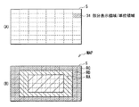
図5は、表示装置1の表示画面Sを模式的に表すものである。表示画面Sは、マトリックス状に配列した部分表示領域31に区分されている。部分表示領域31は、バックライト40の部分発光部41に対応するものである。すなわち、部分発光部41のそれぞれから射出した光は、対応する部分表示領域31を透過するようになっている。また、部分表示領域31は、複数(この例では2つ)の単位領域32に区分されている。
FIG. 5 schematically shows the display screen S of the
ピークレベル検出部11は、部分表示領域31ごとに、映像信号SdispのピークレベルPLを検出する。このピークレベルPLは、最小信号レベルを“0”とし、最大信号レベルを“1”として規格化されたものである。ここで、最小信号レベルは、液晶素子LCにおける光透過率が最小になる映像信号Sdispの信号レベル(いわゆる黒レベル)であり、最大信号レベルは、液晶素子LCにおける光透過率が最大になる映像信号Sdispの信号レベル(いわゆる白レベル)である。そして、ピークレベル検出部11は、部分表示領域31ごとに、その部分表示領域31に属する2つの単位領域32のうちの、ピークレベルPLが検出された単位領域32の位置(ピーク位置PP)を、検出したピークレベルPLとともに、ピークレベル補正部12に供給するようになっている。
The peak
ピークレベル補正部12は、ピークレベル検出部11から供給されたピークレベルPLおよびピーク位置PPに基づいて、ピークレベルPLを補正し、ピークレベルPL2を生成するものである。ピークレベル補正部12は、図1に示したように、補正データマップMAPを有しており、この補正データマップMAPを用いて、ピークレベルPLを補正するようになっている。
The peak
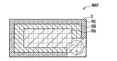
図6は、補正データマップMAPの一例を表すものである。補正データマップMAPは、表示画面Sにおける補正データDTのマップを表すものである。この補正データDTは、単位領域32ごとに設定されている。
FIG. 6 shows an example of the correction data map MAP. The correction data map MAP represents a map of the correction data DT on the display screen S. The correction data DT is set for each
この例では、補正データマップMAPには、補正データDTの値が互いに異なる3つの領域RA〜RCが設定されている。領域RAは、表示画面Sの中央付近に設定され、領域RBは、その領域RAを取り囲むように設定され、領域RCは、その領域RBの外側に設定されている。補正データDTは、領域RAでは“1.0”に設定され、領域RBでは“0.9”に設定され、領域RCでは“0.8”に設定されている。 In this example, in the correction data map MAP, three regions RA to RC having different values of the correction data DT are set. The area RA is set near the center of the display screen S, the area RB is set so as to surround the area RA, and the area RC is set outside the area RB. The correction data DT is set to “1.0” in the region RA, “0.9” in the region RB, and “0.8” in the region RC.
ピークレベル補正部12は、ピークレベル検出部11から供給された、部分表示領域31ごとのピークレベルPLおよびピーク位置PPに基づいて、この補正データマップMAPを用いて、ピークレベルPLを補正する。具体的には、後述するように、ピークレベル補正部12は、まず、補正データマップMAPを用いて、そのピーク位置PPが示す単位領域32における補正データDTを取得する。そして、ピークレベル補正部12は、この補正データDTと、その単位領域32を含む部分表示領域31におけるピークレベルPLと掛け合わせることにより、ピークレベルPLを補正して、ピークレベルPL2を生成する。そして、ピークレベル補正部12は、ピークレベルPL2に基づいて、関数F1により、ゲイン係数G1を求め、信号補正部13に対して供給する。ここで、関数F1は、ピークレベルPL2が小さいほど、ゲイン係数G1が大きくなるような関数である。同様に、ピークレベル補正部12は、ピークレベルPL2に基づいて、関数F2により、輝度係数G2を求める。ここで、関数F2は、ピークレベルPL2が大きいほど、輝度係数G2が大きくなるような関数である。なお、この例では、関数F1,F2を用いたが、これに限定されるものではなく、これに代えて、例えばLUT(Look Up Table)を用いるようにしてもよい。
The peak
信号補正部13は、各部分表示領域31のゲイン係数G1に基づいて、部分表示領域31ごとに、映像信号Sdispの信号レベルを補正し、映像信号Sdisp2として出力するものである。具体的には、信号補正部13は、後述するように、部分表示領域31ごとに、映像信号Sdispの信号レベルに対してゲイン係数G1を乗算することにより補正を行うようになっている。
The
輝度設定部14は、各部分表示領域31の輝度係数G2に基づいて、バックライト40の部分発光部41のそれぞれの輝度を設定するものである。具体的には、輝度設定部14は、後述するように、その部分表示領域31に対応する部分発光部41の輝度を、輝度係数G2に比例する輝度に設定するようになっている。
The
ここで、補正データマップMAPは、本開示における「データマップ」の一具体例に対応し、補正データDTは、本開示における「係数データ」の一具体例に対応する。信号処理部10は、本開示における「処理部」の一具体例に対応する。領域RA〜RCは、本開示における「係数データ領域」の一具体例に対応し、領域RAは、本開示における「特定の係数データ領域」の一具体例に対応する。 Here, the correction data map MAP corresponds to a specific example of “data map” in the present disclosure, and the correction data DT corresponds to a specific example of “coefficient data” in the present disclosure. The signal processing unit 10 corresponds to a specific example of “processing unit” in the present disclosure. The regions RA to RC correspond to a specific example of “coefficient data region” in the present disclosure, and the region RA corresponds to a specific example of “specific coefficient data region” in the present disclosure.
[動作および作用]
続いて、本実施の形態の表示装置1の動作および作用について説明する。
[Operation and Action]
Subsequently, the operation and action of the
(全体動作概要)
まず、図1等を参照して、表示装置1の全体動作概要を説明する。信号処理部10は、映像信号Sdispに基づいて、映像信号Sdisp2を生成するとともに、バックライト40の各部分発光部41の輝度を設定する。具体的には、ピークレベル検出部11は、部分表示領域31ごとに、映像信号SdispのピークレベルPLおよびピーク位置PPを検出する。ピークレベル補正部12は、ピークレベルPLおよびピーク位置PPに基づいて、補正データマップMAPを用いて、ピークレベルPLを補正してピークレベルPL2を生成し、このピークレベルPL2に基づいてゲイン係数G1および輝度係数G2を求める。信号補正部13は、ゲイン係数G1に基づいて、部分表示領域31ごとに映像信号Sdispを補正して映像信号Sdisp2を生成する。輝度設定部14は、輝度係数G2に基づいて、バックライト40の部分発光部41のそれぞれの輝度を設定する。
(Overview of overall operation)
First, an overview of the overall operation of the
表示駆動部20は、液晶表示部30を駆動する。液晶表示部30は、バックライト40から射出した光を変調することにより表示を行う。バックライト駆動部9は、バックライト40を駆動する。バックライト40の各部分発光部41は、バックライト駆動部9から供給される駆動信号に基づいて発光し、液晶表示部30に対してその光を射出する。
The
(信号処理部10の動作)
次に、信号処理部10の動作について、詳細に説明する。
(Operation of the signal processing unit 10)
Next, the operation of the signal processing unit 10 will be described in detail.
図7は、信号処理部10の動作例を表すものである。信号処理部10は、部分表示領域31ごとに、供給された映像信号SdispのピークレベルPLを検出した後、補正データマップMAPを用いてこのピークレベルPLを補正してピークレベルPL2を生成し、そのピークレベルPL2に基づいて、ゲイン係数G1および輝度係数G2を求める。そして、信号処理部10は、そのゲイン係数G1に基づいて映像信号Sdispを補正するとともに、輝度係数G2に基づいてその部分表示領域31に対応する部分発光部41の輝度を設定する。以下に、その詳細を説明する。
FIG. 7 illustrates an operation example of the signal processing unit 10. The signal processing unit 10 detects the peak level PL of the supplied video signal Sdisp for each
まず、信号処理部10のピークレベル検出部11は、部分表示領域31ごとに、映像信号SdispのピークレベルPLおよびピーク位置PPを検出する(ステップS1)。
First, the peak
図8は、図5に示した単位領域A1〜A6における映像信号Sdispの規格化された信号レベルLA1〜LA6の一例を模式的に表すものである。信号レベルLA1〜LA6の各曲線において、横軸は、それぞれ、各単位領域A1〜A6に属する全てのサブ画素SPixを示している。すなわち、信号レベルLA1〜LA6の各曲線は、各単位領域A1〜A6に属する全てのサブ画素SPixに係る信号レベルを示している。 FIG. 8 schematically shows an example of standardized signal levels LA1 to LA6 of the video signal Sdisp in the unit areas A1 to A6 shown in FIG. In each curve of the signal levels LA1 to LA6, the horizontal axis represents all the subpixels SPix belonging to the unit areas A1 to A6, respectively. That is, each curve of the signal levels LA1 to LA6 indicates the signal level relating to all the subpixels SPix belonging to each of the unit areas A1 to A6.
図8に示した例において、例えば、単位領域A1,A2からなる部分表示領域31では、信号レベルLA1,LA2における最大値は0.5(ピークレベルPL)であり、最大値がある単位領域32は単位領域A1(ピーク位置PP)である。
In the example shown in FIG. 8, for example, in the
また、例えば、単位領域A3,A4からなる部分表示領域31では、信号レベルLA3,LA4における最大値は0.5(ピークレベルPL)であり、この最大値がある単位領域32は単位領域A4(ピーク位置PP)である。
Further, for example, in the
同様に、例えば、単位領域A5,A6からなる部分表示領域31では、信号レベルLA3,LA4における最大値は0.5(ピークレベルPL)であり、この最大値がある単位領域32は単位領域A6(ピーク位置PP)である。
Similarly, for example, in the
ピークレベル検出部11は、このようにして、全ての部分表示領域31において、ピークレベルPLおよびピーク位置PPを検出する。なお、この例では、説明の便宜上、このようにピークレベルPLは全て0.5にしたが、これに限定されるものではなく、0から1の範囲内のどのような値も取り得るものである。
In this way, the peak
次に、信号処理部10のピークレベル補正部12は、ピークレベル検出部11が検出したピークレベルPLを補正する(ステップS2)。具体的には、ピークレベル補正部12は、まず、補正データマップMAPを用いて、ピーク位置PPが示す単位領域32における補正データDTを取得する。そして、ピークレベル補正部12は、この補正データDTと、部分表示領域31におけるピークレベルPLと、掛け合わせることにより、ピークレベルPLを補正してピークレベルPL2を生成する。
Next, the peak
例えば、単位領域A1,A2からなる部分表示領域31では、ピーク位置PPは単位領域A1であるので、ピークレベル補正部12は、補正データマップMAP(図6)を用いて、この単位領域A1における補正データDT(1.0)を取得する。すなわち、この部分表示領域31におけるピーク位置PP(単位領域A1)は、領域RAに属する。そして、ピークレベル補正部12は、この補正データDTをピークレベルPL(0.5)と掛け合わせることによりピークレベルPL2(0.5=1.0×0.5)を生成する。
For example, in the
また、単位領域A3,A4からなる部分表示領域31では、ピークレベル補正部12は、ピーク位置PP(単位領域A4)における補正データDT(0.9)を取得する。すなわち、この部分表示領域31におけるピーク位置PP(単位領域A4)は、領域RBに属する。そして、ピークレベル補正部12は、この補正データDTおよびピークレベルPL(0.5)に基づいてピークレベルPL2(0.45=0.9×0.5)を生成する。
In the
同様に、単位領域A5,A6からなる部分表示領域31では、ピークレベル補正部12は、ピーク位置PP(単位領域A6)における補正データDT(0.8)を取得する。すなわち、この部分表示領域31におけるピーク位置PP(単位領域A6)は、領域RCに属する。そして、ピークレベル補正部12は、この補正データDTおよびピークレベルPL(0.5)に基づいてピークレベルPL2(0.4=0.8×0.5)を生成する。
Similarly, in the
ピークレベル補正部12は、このようにして、全ての部分表示領域31において、ピークレベルPLを補正してピークレベルPL2を生成する。
In this way, the peak
次に、信号処理部10は、映像信号Sdispの信号レベルを補正するとともに、バックライト40の各部分発光部41の輝度を設定する(ステップS3)。 Next, the signal processing unit 10 corrects the signal level of the video signal Sdisp and sets the luminance of each partial light emitting unit 41 of the backlight 40 (step S3).
図9は、図8に示した信号レベルの場合におけるステップS3の処理例を表すものであり、(A)は、映像信号Sdispの信号レベルの補正を示し、(B)は、部分発光部41の輝度の設定を示す。 FIG. 9 shows an example of processing in step S3 in the case of the signal level shown in FIG. 8, (A) shows the correction of the signal level of the video signal Sdisp, and (B) shows the partial light emitting unit 41. Indicates the brightness setting.
信号処理部10のピークレベル補正部12は、部分表示領域31ごとに、ピークレベルPL2に基づいて、関数F1を用いてゲイン係数G1を求めるとともに、関数F2を用いて輝度係数G2を求める。そして、信号処理部10の信号補正部13は、図9(A)に示したように、部分表示領域31ごとに、映像信号Sdispの信号レベルにゲイン係数G1を乗算することにより、映像信号Sdispの信号レベルの補正を行う。また、信号処理部10の輝度設定部14は、図9(B)に示したように、部分表示領域31に対応する部分発光部41ごとに、輝度係数G2に比例する輝度に設定する。
The peak
例えば、単位領域A1,A2からなる部分表示領域31では、信号補正部13は、映像信号Sdispの信号レベルに、ピークレベルPL2(0.5)に対応するゲイン係数G1を乗算するとともに(図9(A))、輝度設定部14は、対応する部分発光部41の輝度を、ピークレベルPL2(0.5)に対応する輝度係数G2に比例する輝度に設定する(図9(B))。
For example, in the
また、例えば、単位領域A3,A4からなる部分表示領域31では、信号補正部13は、映像信号Sdispの信号レベルに、ピークレベルPL2(0.45)に対応するゲイン係数G1を乗算するとともに(図9(A))、輝度設定部14は、対応する部分発光部41の輝度を、ピークレベルPL2(0.45)に対応する輝度係数G2に比例する輝度に設定する(図9(B))。この単位領域A3,A4におけるピークレベルPL2(0.45)は、単位領域A1,A2におけるピークレベルPL2(0.5)よりも小さいため、単位領域A3,A4におけるゲイン係数G1は、単位領域A1,A2におけるゲイン係数G1よりも大きく、単位領域A3,A4における輝度係数G2は、単位領域A1,A2における輝度係数G2よりも小さい。
Further, for example, in the
同様に、例えば、単位領域A5,A6からなる部分表示領域31では、信号補正部13は、映像信号Sdispの信号レベルに、ピークレベルPL2(0.4)に対応するゲイン係数G1を乗算するとともに(図9(A))、輝度設定部14は、対応する部分発光部41の輝度を、ピークレベルPL2(0.4)に対応する輝度係数G2に比例する輝度に設定する(図9(B))。この単位領域A5,A6におけるピークレベルPL2(0.4)は、単位領域A3,A4におけるピークレベルPL2(0.45)よりも小さいため、単位領域A5,A6におけるゲイン係数G1は、単位領域A3,A4におけるゲイン係数G1よりも大きく、単位領域A5,A6における輝度係数G2は、単位領域A3,A4における輝度係数G2よりも小さい。
Similarly, for example, in the
信号処理部10は、このようにして、全ての部分表示領域31において、映像信号Sdispの信号レベルを補正するとともに、全ての部分発光部41の輝度を設定する。
In this way, the signal processing unit 10 corrects the signal level of the video signal Sdisp and sets the luminance of all the partial light emitting units 41 in all the
以上で、このフローは終了する。信号処理部10は、映像信号Sdispを介して供給された各フレーム画像に対して、このような処理を行う。 Thus, this flow ends. The signal processing unit 10 performs such processing on each frame image supplied via the video signal Sdisp.
このように、表示装置1では、部分表示領域31ごとに、映像信号Sdispの信号レベルに応じて、対応する部分発光部41の輝度を設定している。これにより、映像信号Sdispの信号レベル(ピークレベルPL)が低いほど、部分発光部41の輝度を下げることができるため、バックライト40の消費電力を低減することができる。
As described above, in the
次に、補正データマップMAPの作用について説明する。補正データマップMAPには、図6に示したように、補正データDTが互いに異なる3つの領域RA〜RCが設定されている。 Next, the operation of the correction data map MAP will be described. In the correction data map MAP, as shown in FIG. 6, three regions RA to RC having different correction data DT are set.
領域RA内にピーク位置PPが検出される部分表示領域31では、補正データDTが1.0であるため、画質を低下させることなく、対応する部分発光部41における輝度を低下させることができる。すなわち、例えば、単位領域A1,A2からなる部分表示領域31(図8,9の左)では、信号レベルをゲイン係数G1倍に補正するとともに、部分発光部41の輝度を輝度係数G2に比例するようにしている。このとき、補正後の信号レベルはいわゆる白レベルを超えることがないため(図9(A))、画質が低下することはない。よって、画質を低下させることなく、消費電力を低減することができる。
In the
また、領域RB内にピーク位置PPが検出される部分表示領域31では、補正データDTが0.9であるため、画質はやや低下するものの、対応する部分発光部41における輝度をより低下させることができる。すなわち、この部分表示領域31では、一部のサブ画素SPixに係る補正後の信号レベルは、白レベルを超え、飽和している(図9(A)の部分W1)。この場合、そのサブ画素SPixの輝度は、所望の輝度よりも低いものとなり、輝度が不足する。また、例えば、ある色のサブ画素SPixの信号レベルのみが飽和した場合には、いわゆる色ずれなどが生ずる。このように、補正後の信号レベルが飽和する場合には、輝度不足や色ずれにより、画質が低下するおそれがある。しかしながら、領域RBは、表示画面Sの中央付近に設定された領域RAを取り囲むように設定されているため(図6)、この領域RAに比べて、観察者が注目する可能性が低いと考えられる。よって、領域RBに係る部分表示領域31では、仮に色ずれなどが生じても、観察者が画質の低下を感じるおそれが低いと考えられる。一方、この領域RBに係る部分発光部41の輝度は、領域RAに係る部分発光部41の輝度よりも低下させることができるため(図9(B))、消費電力をより低減できる。
Further, in the
同様に、領域RC内にピーク位置PPが検出される部分表示領域31では、補正データDTが0.8であるため、領域RAに係る部分表示領域31に比べて、画質はさらにやや低下するものの、対応する部分発光部41における輝度をより低下させることができ、消費電力をより低減できる。
Similarly, in the
このように、表示装置1では、補正データマップMAPを設け、領域RA〜RCごとに、消費電力の低減効果を調整できるようにしている。すなわち、表示画面Sの中央付近に設定された、観察者が最も注目しやすい領域RAでは、画質を低下させることなく、消費電力を低減し、一方、領域RAを取り囲むように設定された、観察者が注目する可能性がより低い領域RB,RCでは、画質をやや犠牲にしつつ、消費電力をさらに低減するようにしている。これにより、表示装置1では、観察者が画質の低下を感じるおそれを抑えつつ、消費電力を効果的に低減することができる。
As described above, the
[効果]
以上のように本実施の形態では、補正データマップを設けたので、部分表示領域ごとに消費電力の設定を調整することができ、自由度の高い電力制御を実現することができる。
[effect]
As described above, since the correction data map is provided in the present embodiment, the power consumption setting can be adjusted for each partial display area, and power control with a high degree of freedom can be realized.
また、本実施の形態では、部分表示領域を複数の単位領域に区分し、単位領域ごとに異なる補正データを設定できるようにしたので、部分表示領域/部分発光部の大きさなどに制限されることなく、領域RA〜RCの形状をより自由に設定することができる。 Further, in the present embodiment, the partial display area is divided into a plurality of unit areas, and different correction data can be set for each unit area. Therefore, the size is limited to the size of the partial display area / partial light emitting unit. Without any problem, the shapes of the regions RA to RC can be set more freely.
また、本実施の形態では、表示画面の中央付近から離れるに従って、消費電力の低減効果が大きくなるようにしたので、観察者が画質の低下を感じるおそれを抑えつつ、消費電力を効果的に低減することができる。 In this embodiment, the effect of reducing the power consumption increases as the distance from the center of the display screen increases. Therefore, the power consumption can be effectively reduced while suppressing the possibility that the observer may experience a decrease in image quality. can do.
[変形例1−1]
上記実施の形態では、領域RA〜RCにおいて、補正データDTを1/0.9/0.8にそれぞれ設定したが、これに限定されるものではなく、これに代えて、例えば、1/0.95/0.9のようにより細かく設定してもよいし、1/0.9/0.85のように細かさが変化するように設定してもよい。
[Modification 1-1]
In the above embodiment, the correction data DT is set to 1 / 0.9 / 0.8 in the regions RA to RC, but the present invention is not limited to this, and instead, for example, 1/0, for example. It may be set more finely as .95 / 0.9 or may be set so that the fineness changes as 1 / 0.9 / 0.85.
また、領域RAにおける補正データDTは1に限定されるものではなく、例えば、1.1/1/0.9のように設定してもよい。この場合の信号処理部10のステップS3における処理例を、図10に示す。本変形例の場合(図10)には、上記実施の形態の場合(図9)と比較すると明らかなように、補正後の信号レベルがやや低下するとともに、部分発光部41の輝度がやや高くなる。具体的には、領域RAに係る部分表示領域31(図10(A)の左)では、補正後の信号レベルの最大値と白レベルとの間にはマージンが生じている(部分W2)。また、領域RCに係る部分表示領域31(図10(A)の右)では、補正後の信号レベルの一部が、白レベルを超えるものの(部分W3)、その超える量は、上記実施の形態の場合(図9)に比べて小さくなっている。すなわち、本変形例では、上記実施の形態の場合に比べて、画質を改善することができる。
Further, the correction data DT in the region RA is not limited to 1, and may be set to 1.1 / 1 / 0.9, for example. An example of processing in step S3 of the signal processing unit 10 in this case is shown in FIG. In the case of this modification (FIG. 10), as is clear from the case of the above embodiment (FIG. 9), the signal level after correction is slightly lowered and the luminance of the partial light emitting unit 41 is slightly high. Become. Specifically, in the
また、上記実施の形態では、3つの領域RA〜RCを設けたが、これに限定されるものではなく、2つの領域を設けてもよいし、4つ以上の領域を設けてもよい。 Moreover, in the said embodiment, although three area | region RA-RC was provided, it is not limited to this, You may provide two area | regions and may provide four or more area | regions.
[変形例1−2]
上記実施の形態では、直下型方式のバックライト40を用いたが、これに限定されるものではなく、これに代えて、例えば、エッジライト方式のバックライトを用いてもよい。以下に、エッジライト方式のバックライト40Bを備えた表示装置1Bについて説明する。
[Modification 1-2]
In the above-described embodiment, the
図11は、エッジライト方式のバックライト40Bの一構成例を表すものである。バックライト40Bは、表示画面Sの上辺および下辺に、それぞれ複数(この例では4つ)の光源49が配置されている。そして、これらの光源49から射出した光は、導光板によって対応する部分発光部43全面に導かれ、液晶表示部30に対して射出する。
FIG. 11 illustrates a configuration example of the edge light type backlight 40B. In the backlight 40B, a plurality (four in this example) of light sources 49 are arranged on the upper side and the lower side of the display screen S, respectively. The light emitted from these light sources 49 is guided to the entire surface of the corresponding partial light emitting unit 43 by the light guide plate and is emitted to the liquid
図12は、表示装置1Bの表示画面Sを模式的に表すものである。表示画面Sは、バックライト40Bの部分発光部43(図11)に対応した複数の部分表示領域33に区分されている。そして、部分表示領域33は、それぞれ、複数(この例では16個)の単位領域32に区分されている。
FIG. 12 schematically shows the display screen S of the display device 1B. The display screen S is divided into a plurality of partial display areas 33 corresponding to the partial light emitting units 43 (FIG. 11) of the backlight 40B. The partial display areas 33 are each divided into a plurality (16 in this example) of
この場合でも、例えば、図6に示した補正データマップMAPを用いることにより、上記実施の形態に係る表示装置1と同様の効果を得ることができる。
Even in this case, for example, by using the correction data map MAP shown in FIG. 6, the same effect as that of the
[変形例1−3]
上記実施の形態では、複数の部分発光部41を有するバックライト40を用いたが、これに限定されるものではなく、これに代えて、例えば、1つの発光部からなるバックライトを用いてもよい。この場合、表示画面Sは、図13に示したように、複数の単位領域32に区分されている。この場合でも、例えば、図6に示した補正データマップMAPを用いることにより、上記実施の形態に係る表示装置1と同様の効果を得ることができる。
[Modification 1-3]
In the above embodiment, the
[変形例1−4]
上記実施の形態では、補正データマップMAPは固定されているものとしたが、これに限定されるものではなく、これに代えて、例えば、動作モードによって補正データマップMAPを変更可能に構成してもよい。例えば、表示装置1がテレビジョン受像機に適用されている場合において、いわゆるホームユースモードでは、領域RA〜RCにおける補正データDTをそれぞれ1/0.9/0.8に設定し、一方、画質優先モードでは、全て1に設定するように構成してもよい。また、補正データDTだけでなく、表示画面Sにおける領域RA〜RCの配置や、これらの領域の数なども変更可能に構成してもよい。
[Modification 1-4]
In the above embodiment, the correction data map MAP is fixed. However, the present invention is not limited to this. For example, the correction data map MAP can be changed according to the operation mode. Also good. For example, when the
また、例えば、映像ソースのコンテンツによって補正データマップを変更可能に構成してもよい。以下に、本変形例に係る表示装置1Fについて説明する。 Further, for example, the correction data map may be changeable depending on the content of the video source. Hereinafter, a display device 1F according to this modification will be described.
図14は、表示装置1Fの一構成例を表すものである。表示装置1Fは、信号処理部10Fを備えている。信号処理部10Fは、コンテンツ検出部15と、ピークレベル補正部12Fとを有している。コンテンツ検出部15は、映像信号Sdispに含まれるコンテンツ情報(スポーツ、ニュース、シネマ、アニメなどのジャンルを示す情報)に基づいて、そのコンテンツを検出するものである。ピークレベル補正部12Fは、コンテンツ検出部15の検出結果に基づいて、補正データマップMAPを変更できるように構成されたものである。具体的には、ピークレベル補正部12Fは、例えば、プリセットされた複数の補正データマップMAPの中から、コンテンツに応じた補正データマップMAPを選択するようになっている。スポーツ番組を表示する際の補正データマップMAPは、例えば、図6のようなものであってもよい。また、シネマ番組を表示する際の補正データマップMAPは、例えば、領域RA〜RCにおける補正データDTを全て1に設定したものであってもよい。なお、この例では、コンテンツ検出部15は、映像信号Sdispに含まれるコンテンツ情報に基づいて、そのコンテンツを検出したが、これに限定されるものではなく、これに代えて、例えばEPG(Electronic Program Guide)に基づいてコンテンツを検出してもよい。
FIG. 14 illustrates a configuration example of the display device 1F. The display device 1F includes a
<2.第2の実施の形態>
次に、第2の実施の形態に係る表示装置2について説明する。本実施の形態は、各部分表示領域31を複数の単位領域32に区分せず、部分表示領域と単位領域とを一対一に対応させたものである。なお、上記第1の実施の形態に係る表示装置1と実質的に同一の構成部分には同一の符号を付し、適宜説明を省略する。
<2. Second Embodiment>
Next, the
本実施の形態に係る表示装置2は、図1に示したように、信号処理部60を備えている。信号処理部60は、ピークレベル検出部61と、ピークレベル補正部62とを有している。
As shown in FIG. 1, the
図15(A)は、表示装置2の表示画面Sを模式的に表すものであり、図15(B)は、補正データマップMAPの一例を表すものである。表示装置2の表示画面Sは、図15(A)に示したように、マトリックス状に配列した部分表示領域34に区分されている。部分表示領域34は、バックライト40の部分発光部41に対応するものである。この部分表示領域34は、上記第1の実施の形態に係る表示装置1の場合とは異なり、複数の単位領域に区分されておらず、単位領域と一対一に対応している。この補正データDTは、単位領域32ごとに設定されている。また、表示装置2に係る補正データマップMAPでは、補正データDTは、図15(B)に示したように、部分表示領域(単位領域)34ごとに設定されている。
FIG. 15A schematically illustrates the display screen S of the
ピークレベル検出部61は、部分表示領域34ごとに、映像信号SdispのピークレベルPLを検出し、その検出結果を、その部分表示領域34の位置PRとともに、ピークレベル補正部62に供給する。すなわち、ピークレベル検出部61は、上記第1の実施の形態に係るピークレベル検出部11とは異なり、ピーク位置PPの代わりに部分表示領域34の位置PRをピークレベル補正部62に供給する。
The peak
ピークレベル補正部62は、ピークレベル検出部61から供給された部分表示領域34ごとのピークレベルPLおよび位置PRに基づいて、補正データマップMAPを用いて、ピークレベルPLを補正する。具体的には、ピークレベル補正部62は、まず、補正データマップMAPを用いて、その位置PRが示す部分表示領域(単位領域)34における補正データDTを取得する。そして、ピークレベル補正部62は、この補正データDTと、その単位領域32を含む部分表示領域31におけるピークレベルPLと掛け合わせることにより、ピークレベルPLを補正して、ピークレベルPL2を生成する。そして、ピークレベル補正部62は、ピークレベルPL2に基づいて、関数F1を用いてゲイン係数G1を求めるとともに、関数F2を用いて輝度係数G2を求める。
The peak
以上のように本実施の形態では、部分表示領域と単位領域を1:1で対応させるようにしたので、信号処理部として、演算能力の低いハードウェアを用いた場合でも、自由度の高い電力制御を実現することができる。その他の効果は、上記第1の実施の形態の場合と同様である。 As described above, in the present embodiment, the partial display area and the unit area are associated with each other at a ratio of 1: 1. Therefore, even when hardware with low calculation capability is used as the signal processing unit, power with a high degree of freedom is provided. Control can be realized. Other effects are the same as in the case of the first embodiment.
[変形例2−1]
上記実施の形態に係る表示装置2に、上記第1の実施の形態の変形例1−1,1−2,1−4を適用してもよい。
[Modification 2-1]
Modifications 1-1, 1-2, and 1-4 of the first embodiment may be applied to the
<3.第3の実施の形態>
次に、第3の実施の形態に係る表示装置3について説明する。本実施の形態は、上記第1の実施の形態に係る表示装置1において、映像信号Sdispに基づいて、補正データマップMAPを動的に変更できるように構成したものである。なお、上記第1の実施の形態に係る表示装置1と実質的に同一の構成部分には同一の符号を付し、適宜説明を省略する。
<3. Third Embodiment>
Next, a
図16は、本実施の形態に係る表示装置3の一構成例を表すものである。表示装置3は、信号処理部50を備えている。信号処理部50は、顔検出部51と、補正データマップ生成部53と、ピークレベル補正部52とを有している。
FIG. 16 illustrates a configuration example of the
顔検出部51は、映像信号Sdispに基づいて、表示画面Sに表示されるべき人の顔を検出し、表示画面Sにおける顔の位置や大きさを求め、これらの情報(顔検出情報IF)を補正データマップ生成部53に供給するものである。補正データマップ生成部53は、顔検出情報IFに基づいて、補正データマップMAPを生成するものである。ピークレベル補正部52は、補正データマップ生成部53から供給された補正データマップMAPを用いて、ピークレベル検出部11において検出されたピークレベルPLを補正し、ピークレベルPL2を生成し、そのピークレベルPL2に基づいて、ゲイン係数G1および輝度係数G2を求めるものである。
The
図17は、本実施の形態に係る補正データマップMAPの一例を表すものである。補正データマップ生成部53は、顔検出情報IFに基づいて、補正データマップMAPを生成する。具体的には、補正データマップ生成部53は、検出した顔に対応する領域を、領域RAに設定し、その領域RAを取り囲むように領域RBを設定し、さらにそれ以外の領域を領域RCに設定することにより、補正データマップMAPを生成する。
FIG. 17 shows an example of the correction data map MAP according to the present embodiment. The correction data map
補正データDTは、上記第1の実施の形態の場合と同様に、領域RAでは“1.0”に設定され、領域RBでは“0.9”に設定され、領域RCでは“0.8”に設定される。すなわち、領域RAに係る部分表示領域31では、画質を低下させることなく、消費電力を低減することができ、領域RB,RCに係る部分表示領域32では、画質をやや犠牲にしつつ、消費電力をさらに低減することができる。
The correction data DT is set to “1.0” in the region RA, “0.9” in the region RB, and “0.8” in the region RC, as in the case of the first embodiment. Set to That is, in the
このように、表示装置3は、映像信号Sdispに基づいて、表示画面Sに表示されるべき人の顔を検出し、その検出した顔に対応する領域を領域RAに設定する。すなわち、観察者は、例えばドラマなどを観察する場合には、一般に、表示された人の顔に注目する可能性が高いと考えられる。また、人の顔を表示する場合は、物体を表示する場合に比べて、例えば色ずれなどが生じたときに、観察者が不自然に感じるおそれが高い。よって、表示装置3では、人の顔を検出し、その表示領域を領域RAに設定することにより、画質を低下させることなくその顔を表示することができる。
As described above, the
また、表示装置3は、顔の表示領域を取り囲むように領域RB,RCを設定する。すなわち、観察者は、上述したように人の顔に注目する可能性が高く、顔以外の領域は、観察者が注目する可能性が低いと考えられるため、顔以外の領域において、仮に色ずれなどが生じても、観察者が画質の低下を感じるおそれが低いと考えられる。よって、表示装置3では、顔の表示領域以外を領域RB,RCに設定することにより、観察者が画質の低下を感じるおそれを抑えつつ、消費電力を効果的に低減することができる。
Further, the
以上のように本実施の形態では、映像信号に基づいて動的に補正データマップを生成するようにしたので、表示内容に応じた自由度の高い電力制御を実現することができる。 As described above, in the present embodiment, since the correction data map is dynamically generated based on the video signal, it is possible to realize power control with a high degree of freedom according to the display content.
また、本実施の形態では、顔検出部を設け、顔が表示される領域では高い画質により表示を行い、それ以外の領域では、消費電力を低減するようにしたので、観察者が画質の低下を感じるおそれを抑えつつ、消費電力を効果的に低減することができる。 In this embodiment, a face detection unit is provided so that display is performed with high image quality in the area where the face is displayed, and power consumption is reduced in other areas. It is possible to effectively reduce power consumption while suppressing the fear of feeling.
その他の効果は、上記第1の実施の形態の場合と同様である。 Other effects are the same as in the case of the first embodiment.
[変形例3−1]
上記実施の形態では、表示画面Sに表示されるべき人の顔を検出したが、これに限定されるものではなく、これに代えて、もしくはこれに加えて、例えば、字幕やテロップなどを検出してもよい。これにより、観察者が注目する可能性が高い字幕やテロップなどを、画質を低下させることなく表示することができる。
[Modification 3-1]
In the above embodiment, a human face to be displayed on the display screen S is detected. However, the present invention is not limited to this. For example, subtitles and telops are detected instead of or in addition to this. May be. As a result, it is possible to display subtitles, telops, and the like that are likely to be noticed by the observer without reducing the image quality.
[変形例3−2]
上記実施の形態では、観察者が注目する可能性が高いものを検出し、その表示領域を領域RAに設定したが、これに限定されるものではなく、これに代えて、例えば、観察者が注目する可能性が低いものを検出し、その表示領域を領域RCに設定してもよい。具体的には、表示装置3を例えばテレビ会議システムに適用した場合において、自分の顔が表示される領域を領域RCに設定することができる。これにより、相手の顔が表示される領域では高い画質により表示を行い、自分の顔が表示される領域では、画質を犠牲にして消費電力を低減することができる。
[Modification 3-2]
In the above embodiment, an object that is likely to be noticed by the observer is detected, and the display area is set to the area RA. However, the present invention is not limited to this, and instead, for example, the observer What has a low possibility of paying attention may be detected, and the display area may be set to the area RC. Specifically, when the
[変形例3−3]
上記実施の形態に係る表示装置3に、上記第1の実施の形態の変形例1−1〜1−4を適用してもよい。
[Modification 3-3]
Modifications 1-1 to 1-4 of the first embodiment may be applied to the
[変形例3−4]
上記実施の形態では、上記第1の実施の形態に係る表示装置1において、補正データマップMAPを動的に変更できるよう構成したが、これに限定されるものではなく、上記第2の実施の形態に係る表示装置2において、補正データマップMAPを動的に変更できるように構成してもよい。
[Modification 3-4]
In the above embodiment, the
以上、いくつかの実施の形態および変形例を挙げて本技術を説明したが、本技術はこれらの実施の形態等には限定されず、種々の変形が可能である。 The present technology has been described above with some embodiments and modifications. However, the present technology is not limited to these embodiments and the like, and various modifications are possible.
例えば、上記第3の実施の形態では、検出した顔の位置に領域RAを設定し、その顔の表示領域を取り囲むように領域RB,RCを設定したが、これに限定されるものではない。例えば、図18に示したように、上記第1および第2の実施の形態に係る補正データマップMAP(例えば図6)において、顔が検出された領域をも領域RAに設定してもよい。これにより、表示画面Sに顔が表示されていない場合には、上記第1および第2の実施の形態に係る表示装置1,2のように動作し、表示画面Sに顔が表示される場合には、その顔が表示される領域について、画質を低下させることなく、消費電力を効果的に低減することができる。
For example, in the third embodiment, the area RA is set at the detected face position, and the areas RB and RC are set so as to surround the display area of the face. However, the present invention is not limited to this. For example, as shown in FIG. 18, in the correction data map MAP (for example, FIG. 6) according to the first and second embodiments, an area where a face is detected may be set as the area RA. Thereby, when the face is not displayed on the display screen S, it operates like the
なお、本技術は以下のような構成とすることができる。 In addition, this technique can be set as the following structures.
(1)映像信号に基づいて画像を表示する液晶表示部と、
バックライトと、
表示画面またはその表示画面を区分してなる複数の部分表示領域のそれぞれにおける前記映像信号のピークレベルと、表示画面上の参照位置と係数データとを関連づけて構成されたデータマップから取得した前記係数データとに基づいて、前記映像信号を補正するとともに、前記バックライトの輝度を設定する処理部と
を備えた表示装置。
(1) a liquid crystal display unit for displaying an image based on a video signal;
With backlight,
The coefficient obtained from a data map configured by associating a peak level of the video signal in each of the display screen or a plurality of partial display areas obtained by dividing the display screen, a reference position on the display screen, and coefficient data And a processing unit that corrects the video signal based on the data and sets the luminance of the backlight.
(2)前記ピークレベルは、各部分表示領域に表示すべき画像におけるピークレベルであり、
前記処理部は、前記データマップを用いて、各部分表示領域において前記ピークレベルが生じる表示画面上の位置を前記参照位置として、その参照位置に関連づけられた係数データを取得する
前記(1)に記載の表示装置。
(2) The peak level is a peak level in an image to be displayed in each partial display area,
The processing unit uses the data map to obtain coefficient data associated with the reference position, using the position on the display screen where the peak level occurs in each partial display area as the reference position. The display device described.
(3)前記ピークレベルは、各部分表示領域に表示すべき画像におけるピークレベルであり、
前記処理部は、前記データマップを用いて、各部分表示領域の表示画面上の位置を前記参照位置として、その参照位置に関連づけられた係数データを取得する
前記(1)に記載の表示装置。
(3) The peak level is a peak level in an image to be displayed in each partial display area,
The display device according to (1), wherein the processing unit obtains coefficient data associated with the reference position, using the data map as a position on the display screen of each partial display area as the reference position.
(4)前記バックライトは、各部分表示領域に対応する部分発光部を複数有し、
前記処理部は、前記ピークレベルおよび前記係数データに基づいて、各部分表示領域に係る前記映像信号を補正するとともに、対応する部分発光部の輝度を設定する
前記(2)または(3)に記載の表示装置。
(4) The backlight includes a plurality of partial light emitting units corresponding to the partial display areas,
The processing unit corrects the video signal related to each partial display area based on the peak level and the coefficient data, and sets the luminance of the corresponding partial light emitting unit. (2) or (3) Display device.
(5)前記ピークレベルは、表示画面に表示すべき画像におけるピークレベルであり、
前記処理部は、前記データマップを用いて、前記ピークレベルが生じる表示画面上の位置を前記参照位置として、その参照位置に関連づけられた係数データを取得する
前記(1)に記載の表示装置。
(5) The peak level is a peak level in an image to be displayed on the display screen,
The display unit according to (1), wherein the processing unit acquires coefficient data associated with the reference position using the data map, with the position on the display screen where the peak level occurs as the reference position.
(6)前記データマップは、前記係数データが互いに異なる複数の係数データ領域に区分されている
前記(1)から(5)のいずれかに記載の表示装置。
(6) The display device according to any one of (1) to (5), wherein the data map is divided into a plurality of coefficient data areas in which the coefficient data is different from each other.
(7)前記処理部は、前記参照位置が、前記複数の係数データ領域のうちの特定の係数データ領域に属する場合には、その参照位置がその他の係数データ領域に属する場合に比べて、前記バックライトの輝度を高く設定するとともに、前記液晶表示部の透過率を低くするように前記映像信号を補正する
前記(6)に記載の表示装置。
(7) When the reference position belongs to a specific coefficient data area of the plurality of coefficient data areas, the processing unit compares the reference position to other coefficient data areas as compared to the case where the reference position belongs to another coefficient data area. The display device according to (6), wherein the luminance of the backlight is set high, and the video signal is corrected so as to reduce the transmittance of the liquid crystal display unit.
(8)前記特定の係数データ領域は、表示画面の中央付近に対応する領域に設定されている
前記(7)に記載の表示装置。
(8) The display device according to (7), wherein the specific coefficient data area is set in an area corresponding to a vicinity of a center of a display screen.
(9)前記映像信号に基づいて、表示すべき画像において所定画像を識別する画像識別部を備えた
前記(7)に記載の表示装置。
(9) The display device according to (7), further including an image identification unit that identifies a predetermined image in an image to be displayed based on the video signal.
(10)前記特定の係数データ領域は、前記所定画像が識別された領域である
前記(9)に記載の表示装置。
(10) The display device according to (9), wherein the specific coefficient data area is an area in which the predetermined image is identified.
(11)前記特定の係数データ領域は、表示画面の中央付近に対応する領域と、前記所定画像が識別された領域とからなる
前記(9)に記載の表示装置。
(11) The display device according to (9), wherein the specific coefficient data area includes an area corresponding to the vicinity of the center of the display screen and an area where the predetermined image is identified.
(12)前記所定画像は顔画像である
前記(9)から(11)のいずれかに記載の表示装置。
(12) The display device according to any one of (9) to (11), wherein the predetermined image is a face image.
(13)前記所定画像は、表示画像において観察者の注目度の高い部分の画像である
前記(9)から(12)のいずれかに記載の表示装置。
(13) The display device according to any one of (9) to (12), wherein the predetermined image is an image of a portion having a high degree of attention of an observer in the display image.
(14)前記特定の係数データ領域を含むデータマップを生成するデータマップ生成部を備えている
前記(7)から(13)のいずれかに記載の表示装置。
(14) The display device according to any one of (7) to (13), further including a data map generation unit that generates a data map including the specific coefficient data region.
(15)前記表示装置は、複数の動作モードを有し、
前記処理部は、動作モードに応じて、参照するデータマップを決定する
前記(1)から(14)のいずれかに記載の表示装置。
(15) The display device has a plurality of operation modes,
The display unit according to any one of (1) to (14), wherein the processing unit determines a data map to be referred to according to an operation mode.
(16)前記処理部は、表示するコンテンツに応じて、参照するデータマップを決定する
前記(1)から(15)のいずれかに記載の表示装置。
(16) The display device according to any one of (1) to (15), wherein the processing unit determines a data map to be referred to according to content to be displayed.
(17)映像信号に基づいて画像を表示する液晶表示部と、
バックライトと、
表示画面またはその表示画面を区分してなる複数の部分表示領域のそれぞれにおける前記映像信号のピークレベルと、そのピークレベルが生じる表示画面上の位置であるピーク位置とに基づいて、前記映像信号を補正するとともに、前記バックライトの輝度を設定する処理部と
を備えた表示装置。
(17) a liquid crystal display unit for displaying an image based on the video signal;
With backlight,
Based on the peak level of the video signal in each of the display screen or a plurality of partial display areas obtained by dividing the display screen, and the peak position that is the position on the display screen where the peak level occurs, the video signal is And a processing unit that corrects and sets the luminance of the backlight.
(18)映像信号に基づいて画像を表示する液晶表示部と、
複数の部分発光部を有するバックライトと、
各部分発光部に対応する部分表示領域に表示すべき画像における前記映像信号のピークレベルと、その部分表示領域の位置とに基づいて、前記映像信号を補正するとともに、前記部分発光部の輝度を設定する処理部と
を備えた表示装置。
(18) a liquid crystal display unit for displaying an image based on the video signal;
A backlight having a plurality of partial light emitting units;
The video signal is corrected based on the peak level of the video signal in the image to be displayed in the partial display area corresponding to each partial light emitting section and the position of the partial display area, and the luminance of the partial light emitting section is adjusted. A display device comprising a processing unit for setting.
(19)表示画面またはその表示画面を区分してなる複数の部分表示領域のそれぞれにおける前記映像信号のピークレベルと、表示画面上の位置と係数データとを関連づけて構成されたデータマップから取得した前記係数データとに基づいて、映像信号を補正するとともに、前記バックライトの輝度を設定し、補正された映像信号に基づいて画像を表示する
表示方法。
(19) Obtained from a data map configured by associating the peak level of the video signal in each of the display screen or a plurality of partial display areas obtained by dividing the display screen, the position on the display screen, and coefficient data A display method that corrects a video signal based on the coefficient data, sets brightness of the backlight, and displays an image based on the corrected video signal.
1,1F,2,3…表示装置、9…バックライト駆動部、10,10F,50…信号処理部、11,61…ピークレベル検出部、12,12F,52,62…ピークレベル補正部、13…信号補正部、14…輝度設定部、15…コンテンツ検出部、20…表示駆動部、21…タイミング制御部、22…ゲートドライバ、23…データドライバ、30…液晶表示部、31,33…部分表示領域、32,A1〜A6…単位領域、34…部分表示領域/単位領域、40,40B…バックライト、41…部分発光部、43…部分発光部/導光板、49…光源、51…顔検出部、53…補正データマップ生成部、DT…補正データ、GCL…ゲート線、IF…顔検出情報、LC…液晶素子、MAP…補正データマップ、Pix…画素、PL…ピークレベル、PP…ピーク位置、RA〜RC…領域、S…表示画面、Sdisp,Sdisp2,Sdisp3…映像信号、SGL…データ線、SPix…サブ画素、Tr…TFT素子。
DESCRIPTION OF
Claims (20)
バックライトと、
表示画面またはその表示画面を区分してなる複数の部分表示領域のそれぞれにおける前記映像信号のピークレベルと、表示画面上の参照位置と係数データとを関連づけて構成されたデータマップから取得した前記係数データとに基づいて、前記映像信号を補正するとともに、前記バックライトの輝度を設定する処理部と
を備えた表示装置。 A liquid crystal display for displaying an image based on the video signal;
With backlight,
The coefficient obtained from a data map configured by associating a peak level of the video signal in each of the display screen or a plurality of partial display areas obtained by dividing the display screen, a reference position on the display screen, and coefficient data And a processing unit that corrects the video signal based on the data and sets the luminance of the backlight.
前記処理部は、前記データマップを用いて、各部分表示領域において前記ピークレベルが生じる表示画面上の位置を前記参照位置として、その参照位置に関連づけられた係数データを取得する
請求項1に記載の表示装置。 The peak level is a peak level in an image to be displayed in each partial display area,
The processing unit acquires coefficient data associated with the reference position, using the data map as a reference position at a position on the display screen where the peak level occurs in each partial display region. Display device.
前記処理部は、前記ピークレベルおよび前記係数データに基づいて、各部分表示領域に係る前記映像信号を補正するとともに、対応する部分発光部の輝度を設定する
請求項2に記載の表示装置。 The backlight has a plurality of partial light emitting portions corresponding to each partial display area,
The display device according to claim 2, wherein the processing unit corrects the video signal related to each partial display region based on the peak level and the coefficient data, and sets the luminance of the corresponding partial light emitting unit.
前記処理部は、前記データマップを用いて、各部分表示領域の表示画面上の位置を前記参照位置として、その参照位置に関連づけられた係数データを取得する
請求項1に記載の表示装置。 The peak level is a peak level in an image to be displayed in each partial display area,
The display device according to claim 1, wherein the processing unit obtains coefficient data associated with the reference position using the position of the partial display area on the display screen as the reference position using the data map.
前記処理部は、前記ピークレベルおよび前記係数データに基づいて、各部分表示領域に係る前記映像信号を補正するとともに、対応する部分発光部の輝度を設定する
請求項4に記載の表示装置。 The backlight has a plurality of partial light emitting portions corresponding to each partial display area,
The display device according to claim 4, wherein the processing unit corrects the video signal related to each partial display area based on the peak level and the coefficient data, and sets the luminance of the corresponding partial light emitting unit.
前記処理部は、前記データマップを用いて、前記ピークレベルが生じる表示画面上の位置を前記参照位置として、その参照位置に関連づけられた係数データを取得する
請求項1に記載の表示装置。 The peak level is a peak level in an image to be displayed on a display screen,
The display device according to claim 1, wherein the processing unit uses the data map to obtain coefficient data associated with the reference position with the position on the display screen where the peak level occurs as the reference position.
請求項2に記載の表示装置。 The display device according to claim 2, wherein the data map is divided into a plurality of coefficient data areas in which the coefficient data are different from each other.
請求項7に記載の表示装置。 The processing unit, when the reference position belongs to a specific coefficient data area of the plurality of coefficient data areas, compared to the case where the reference position belongs to another coefficient data area. The display device according to claim 7, wherein the video signal is corrected so that the luminance is set high and the transmittance of the liquid crystal display unit is lowered.
請求項8に記載の表示装置。 The display device according to claim 8, wherein the specific coefficient data area is set in an area corresponding to the vicinity of the center of the display screen.
請求項8に記載の表示装置。 The display device according to claim 8, further comprising an image identification unit that identifies a predetermined image in an image to be displayed based on the video signal.
請求項10に記載の表示装置。 The display device according to claim 10, wherein the specific coefficient data area is an area in which the predetermined image is identified.
請求項10に記載の表示装置。 The display device according to claim 10, wherein the specific coefficient data area includes an area corresponding to a vicinity of a center of a display screen and an area where the predetermined image is identified.
請求項10に記載の表示装置。 The display device according to claim 10, wherein the predetermined image is a face image.
請求項10に記載の表示装置。 The display device according to claim 10, wherein the predetermined image is an image of a portion of the display image where the degree of attention of the observer is high.
請求項8に記載の表示装置。 The display device according to claim 8, further comprising a data map generation unit configured to generate a data map including the specific coefficient data region.
前記処理部は、動作モードに応じて、参照するデータマップを決定する
請求項1に記載の表示装置。 The display device has a plurality of operation modes,
The display device according to claim 1, wherein the processing unit determines a data map to be referenced according to an operation mode.
請求項1に記載の表示装置。 The display device according to claim 1, wherein the processing unit determines a data map to be referenced according to content to be displayed.
バックライトと、
表示画面またはその表示画面を区分してなる複数の部分表示領域のそれぞれにおける前記映像信号のピークレベルと、そのピークレベルが生じる表示画面上の位置であるピーク位置とに基づいて、前記映像信号を補正するとともに、前記バックライトの輝度を設定する処理部と
を備えた表示装置。 A liquid crystal display for displaying an image based on the video signal;
With backlight,
Based on the peak level of the video signal in each of the display screen or a plurality of partial display areas obtained by dividing the display screen, and the peak position that is the position on the display screen where the peak level occurs, the video signal is And a processing unit that corrects and sets the luminance of the backlight.
複数の部分発光部を有するバックライトと、
各部分発光部に対応する部分表示領域における前記映像信号のピークレベルと、その部分表示領域の位置とに基づいて、前記映像信号を補正するとともに、前記部分発光部の輝度を設定する処理部と
を備えた表示装置。 A liquid crystal display for displaying an image based on the video signal;
A backlight having a plurality of partial light emitting units;
A processing unit that corrects the video signal based on a peak level of the video signal in a partial display region corresponding to each partial light emitting unit and a position of the partial display region, and sets a luminance of the partial light emitting unit; A display device comprising:
表示方法。 The coefficient data obtained from the data map configured by associating the peak level of the video signal in each of the display screen or a plurality of partial display areas obtained by dividing the display screen, the position on the display screen, and the coefficient data A display method that corrects the video signal based on the above and sets the luminance of the backlight and displays an image based on the corrected video signal.
Priority Applications (7)
| Application Number | Priority Date | Filing Date | Title |
|---|---|---|---|
| JP2011246770A JP2013104912A (en) | 2011-11-10 | 2011-11-10 | Display device and display method |
| EP19158011.7A EP3506249A1 (en) | 2011-11-10 | 2012-11-02 | Display device and display method |
| US13/667,529 US9159273B2 (en) | 2011-11-10 | 2012-11-02 | Display device and display method |
| EP12191148.1A EP2592618B1 (en) | 2011-11-10 | 2012-11-02 | Display device and display method |
| CN201210433438.XA CN103106879B (en) | 2011-11-10 | 2012-11-02 | Display device and display methods |
| US14/844,144 US9583052B2 (en) | 2011-11-10 | 2015-09-03 | Display device and display method |
| US15/409,994 US9922602B2 (en) | 2011-11-10 | 2017-01-19 | Display device and display method |
Applications Claiming Priority (1)
| Application Number | Priority Date | Filing Date | Title |
|---|---|---|---|
| JP2011246770A JP2013104912A (en) | 2011-11-10 | 2011-11-10 | Display device and display method |
Publications (2)
| Publication Number | Publication Date |
|---|---|
| JP2013104912A true JP2013104912A (en) | 2013-05-30 |
| JP2013104912A5 JP2013104912A5 (en) | 2014-11-27 |
Family
ID=47428472
Family Applications (1)
| Application Number | Title | Priority Date | Filing Date |
|---|---|---|---|
| JP2011246770A Abandoned JP2013104912A (en) | 2011-11-10 | 2011-11-10 | Display device and display method |
Country Status (4)
| Country | Link |
|---|---|
| US (3) | US9159273B2 (en) |
| EP (2) | EP3506249A1 (en) |
| JP (1) | JP2013104912A (en) |
| CN (1) | CN103106879B (en) |
Cited By (5)
| Publication number | Priority date | Publication date | Assignee | Title |
|---|---|---|---|---|
| WO2015141273A1 (en) * | 2014-03-20 | 2015-09-24 | 富士フイルム株式会社 | Display device and control method thereof, and finder device |
| CN105931612A (en) * | 2016-07-13 | 2016-09-07 | 京东方科技集团股份有限公司 | Source electrode driving circuit, source electrode driving method and display device |
| KR20160137535A (en) | 2014-03-31 | 2016-11-30 | 소니 주식회사 | Image processing device, image processing method, and program |
| WO2019239918A1 (en) * | 2018-06-15 | 2019-12-19 | シャープ株式会社 | Control device, display device, and control method |
| US10593289B2 (en) | 2014-03-28 | 2020-03-17 | Sony Corporation | Information processing system, image processing apparatus, image processing method, and program for color conversion of an image by selecting an electricity consumption minimum value |
Families Citing this family (9)
| Publication number | Priority date | Publication date | Assignee | Title |
|---|---|---|---|---|
| JP2013104912A (en) * | 2011-11-10 | 2013-05-30 | Sony Corp | Display device and display method |
| KR102074719B1 (en) * | 2013-10-08 | 2020-02-07 | 엘지디스플레이 주식회사 | Organic light emitting display device |
| JP6326219B2 (en) * | 2013-11-26 | 2018-05-16 | 圭祐 戸田 | Display device and display method |
| JP6165681B2 (en) * | 2014-06-27 | 2017-07-19 | 富士フイルム株式会社 | Image display device and image display method |
| US10089938B2 (en) * | 2015-06-03 | 2018-10-02 | Japan Display Inc. | Display device with sidelight illumination and luminance correction |
| US10114447B2 (en) * | 2015-12-10 | 2018-10-30 | Samsung Electronics Co., Ltd. | Image processing method and apparatus for operating in low-power mode |
| US20170205977A1 (en) | 2016-01-18 | 2017-07-20 | Michael Benjamin Selkowe Fertik | Methods for displaying an e-book using a combination of colors for text and background that have a reduced myopiagenic effect |
| CN107665681B (en) * | 2017-09-26 | 2020-06-05 | 武汉华星光电技术有限公司 | Liquid crystal display driving method, system and computer readable medium |
| WO2020058034A1 (en) * | 2018-09-18 | 2020-03-26 | Signify Holding B.V. | Pixelated color tunable luminaire |
Family Cites Families (15)
| Publication number | Priority date | Publication date | Assignee | Title |
|---|---|---|---|---|
| EP1564478B1 (en) * | 2002-10-22 | 2012-01-25 | Sharp Kabushiki Kaisha | Backlight unit and liquid crystal display unit using backlight unit |
| JP4029743B2 (en) * | 2003-02-24 | 2008-01-09 | ソニー株式会社 | Backlight |
| TWI330270B (en) * | 2005-03-29 | 2010-09-11 | Chi Mei Optoelectronics Corp | Region-based displayer and display method thereof |
| JP2008176211A (en) * | 2007-01-22 | 2008-07-31 | Hitachi Ltd | Liquid crystal display device and method of controlling brightness thereof |
| KR100885285B1 (en) | 2007-05-08 | 2009-02-23 | 닛뽕빅터 가부시키가이샤 | Liquid crystal display apparatus and image display method used therein |
| JP2009042652A (en) | 2007-08-10 | 2009-02-26 | Victor Co Of Japan Ltd | Liquid crystal display device and image display method thereof |
| US8139022B2 (en) * | 2007-05-08 | 2012-03-20 | Victor Company Of Japan, Limited | Liquid crystal display device and image display method thereof |
| KR20090044292A (en) * | 2007-10-31 | 2009-05-07 | 삼성전자주식회사 | Display device and driving method thereof |
| JP2010044180A (en) * | 2008-08-12 | 2010-02-25 | Victor Co Of Japan Ltd | Liquid crystal display device and video signal processing method used for the same |
| KR100959594B1 (en) * | 2008-05-01 | 2010-05-27 | 닛뽕빅터 가부시키가이샤 | Liquid crystal display apparatus and image display method used therefor |
| JP2010113099A (en) | 2008-11-05 | 2010-05-20 | Sharp Corp | Display device and display control method |
| JP5495025B2 (en) * | 2009-12-22 | 2014-05-21 | ソニー株式会社 | Image processing apparatus and method, and program |
| JP5531785B2 (en) | 2010-05-27 | 2014-06-25 | 新日鐵住金株式会社 | Directional electrical steel sheet and tension insulating film coated directional electrical steel sheet |
| JP5661336B2 (en) * | 2010-05-28 | 2015-01-28 | 日立マクセル株式会社 | Liquid crystal display |
| JP2013104912A (en) * | 2011-11-10 | 2013-05-30 | Sony Corp | Display device and display method |
-
2011
- 2011-11-10 JP JP2011246770A patent/JP2013104912A/en not_active Abandoned
-
2012
- 2012-11-02 US US13/667,529 patent/US9159273B2/en not_active Expired - Fee Related
- 2012-11-02 EP EP19158011.7A patent/EP3506249A1/en not_active Withdrawn
- 2012-11-02 CN CN201210433438.XA patent/CN103106879B/en not_active Expired - Fee Related
- 2012-11-02 EP EP12191148.1A patent/EP2592618B1/en not_active Not-in-force
-
2015
- 2015-09-03 US US14/844,144 patent/US9583052B2/en active Active
-
2017
- 2017-01-19 US US15/409,994 patent/US9922602B2/en active Active
Cited By (8)
| Publication number | Priority date | Publication date | Assignee | Title |
|---|---|---|---|---|
| WO2015141273A1 (en) * | 2014-03-20 | 2015-09-24 | 富士フイルム株式会社 | Display device and control method thereof, and finder device |
| JPWO2015141273A1 (en) * | 2014-03-20 | 2017-04-06 | 富士フイルム株式会社 | Display device and finder device |
| US10109242B2 (en) | 2014-03-20 | 2018-10-23 | Fujifilm Corporation | Display device and finder device |
| US10593289B2 (en) | 2014-03-28 | 2020-03-17 | Sony Corporation | Information processing system, image processing apparatus, image processing method, and program for color conversion of an image by selecting an electricity consumption minimum value |
| KR20160137535A (en) | 2014-03-31 | 2016-11-30 | 소니 주식회사 | Image processing device, image processing method, and program |
| US10163402B2 (en) | 2014-03-31 | 2018-12-25 | Sony Corporation | Image processing apparatus and image processing method |
| CN105931612A (en) * | 2016-07-13 | 2016-09-07 | 京东方科技集团股份有限公司 | Source electrode driving circuit, source electrode driving method and display device |
| WO2019239918A1 (en) * | 2018-06-15 | 2019-12-19 | シャープ株式会社 | Control device, display device, and control method |
Also Published As
| Publication number | Publication date |
|---|---|
| US9922602B2 (en) | 2018-03-20 |
| US20170132981A1 (en) | 2017-05-11 |
| US20130120475A1 (en) | 2013-05-16 |
| US20150379943A1 (en) | 2015-12-31 |
| CN103106879B (en) | 2019-08-20 |
| US9159273B2 (en) | 2015-10-13 |
| EP2592618B1 (en) | 2019-08-14 |
| US9583052B2 (en) | 2017-02-28 |
| EP3506249A1 (en) | 2019-07-03 |
| EP2592618A1 (en) | 2013-05-15 |
| CN103106879A (en) | 2013-05-15 |
Similar Documents
| Publication | Publication Date | Title |
|---|---|---|
| US9922602B2 (en) | Display device and display method | |
| US10176745B2 (en) | Data conversion unit and method | |
| JP5460435B2 (en) | Image display device and control method of image display device | |
| WO2013035635A1 (en) | Image display device and image display method | |
| US8970470B2 (en) | Display apparatus and control method thereof | |
| US20100013872A1 (en) | Liquid crystal display device | |
| JP2009139470A (en) | Image display device, and image display method | |
| JP2010175913A (en) | Image display apparatus | |
| JP5671608B2 (en) | Image display device and image display method | |
| EP2175312B1 (en) | Liquid crystal display device, television receiver, and illumination device | |
| JP2011242665A (en) | Image display device | |
| CN106128375B (en) | The data processing method of transparent liquid crystal display | |
| US9355614B2 (en) | Image quality processing method and display device using the same | |
| WO2012036058A1 (en) | Drive circuit, drive method, and display device | |
| JP5359191B2 (en) | Liquid crystal display | |
| KR20180052836A (en) | Display apparatus and driving method thereof | |
| JP2006243576A (en) | Liquid crystal display device | |
| JP5926918B2 (en) | Multi display system | |
| WO2013018822A1 (en) | Image display device and image display method | |
| KR102287512B1 (en) | Transparent image display apparatus | |
| JP5679192B2 (en) | Liquid crystal panel drive device and liquid crystal display device using the same | |
| WO2013080907A1 (en) | Image display device and image display method | |
| JP5242752B2 (en) | Image processing device | |
| JP2012064588A (en) | Backlight device and control method of backlight device | |
| JP2010197926A (en) | Crosstalk correction table acquisition device |
Legal Events
| Date | Code | Title | Description |
|---|---|---|---|
| A521 | Written amendment |
Free format text: JAPANESE INTERMEDIATE CODE: A523 Effective date: 20141015 |
|
| A621 | Written request for application examination |
Free format text: JAPANESE INTERMEDIATE CODE: A621 Effective date: 20141015 |
|
| A762 | Written abandonment of application |
Free format text: JAPANESE INTERMEDIATE CODE: A762 Effective date: 20150406 |