JP2013102417A5 - - Google Patents
Download PDFInfo
- Publication number
- JP2013102417A5 JP2013102417A5 JP2012172302A JP2012172302A JP2013102417A5 JP 2013102417 A5 JP2013102417 A5 JP 2013102417A5 JP 2012172302 A JP2012172302 A JP 2012172302A JP 2012172302 A JP2012172302 A JP 2012172302A JP 2013102417 A5 JP2013102417 A5 JP 2013102417A5
- Authority
- JP
- Japan
- Prior art keywords
- clock
- circuit
- branch point
- signal
- sequential
- Prior art date
- Legal status (The legal status is an assumption and is not a legal conclusion. Google has not performed a legal analysis and makes no representation as to the accuracy of the status listed.)
- Pending
Links
- 239000004065 semiconductor Substances 0.000 claims description 3
- 238000004519 manufacturing process Methods 0.000 description 4
- 230000002411 adverse Effects 0.000 description 1
- 230000015572 biosynthetic process Effects 0.000 description 1
- UIIMBOGNXHQVGW-UHFFFAOYSA-M buffer Substances [Na+].OC([O-])=O UIIMBOGNXHQVGW-UHFFFAOYSA-M 0.000 description 1
- 230000001934 delay Effects 0.000 description 1
- 238000010586 diagram Methods 0.000 description 1
- 230000000694 effects Effects 0.000 description 1
- 230000000051 modifying Effects 0.000 description 1
- 229920000729 poly(L-lysine) polymer Polymers 0.000 description 1
- 230000001360 synchronised Effects 0.000 description 1
- 238000003786 synthesis reaction Methods 0.000 description 1
- 230000002194 synthesizing Effects 0.000 description 1
Images


Description
本発明の一側面によれば、半導体集積回路のクロック分配回路であって、クロック信号を生成するクロック生成回路と、前記クロック信号が分配されるクロック分配網と、前記クロック分配網の分岐点を通じて分配されるクロック信号で動作する順序回路とを有し、前記クロック生成回路は、前記分岐点から分岐した前記クロック信号をフィードバック信号として入力し、該入力したフィードバック信号とリファレンスクロック信号とに基づいて、前記クロック信号を前記クロック分配網へ出力するように構成され、前記分岐点は、前記クロック分配網の順序回路の前段のクロックドライバのうち、前記クロック生成回路の近傍にあるクロックドライバに設けられることを特徴とするクロック分配回路が提供される。 According to one aspect of the present invention, there is provided a clock distribution circuit for a semiconductor integrated circuit, a clock generation circuit for generating a clock signal, a clock distribution network to which the clock signal is distributed, and a branch point of the clock distribution network. possess a sequential circuit that operates at a clock signal distributed, the clock generation circuit receives the clock signal branched from the branch point as a feedback signal, based on a feedback signal obtained by the input and the reference clock signal The clock signal is output to the clock distribution network, and the branch point is provided in a clock driver in the vicinity of the clock generation circuit among the clock drivers in the previous stage of the sequential circuit of the clock distribution network. A clock distribution circuit is provided.
まず、図6のフローチャートを参照して、レイアウトデータに基づいてフィードバックパスを設ける方法について説明する。ここでは、例えば、通常のCTS (Clock Tree Synthesis) 手法などによってクロック配線が実行され詳細な配置配線が実行された後のレイアウトデータが活用される。はじめに、レイアウトデータに基づいてクロック生成回路の近傍に存在する順序回路を抽出する(S601)。図3では、順序回路26n1,26n2,26n3がクロック生成回路の近傍に存在する。よってここでは、フィードバックパス分岐点は、クロック分配回路網の最終段のクロックドライバ25n1,25n2,25n3のうちクロック生成回路23近傍にあるいずれかのクロックドライバ25n1,25n2,25n3の出力端子側の位置に設定される。 First, a method for providing a feedback path based on layout data will be described with reference to the flowchart of FIG. Here, for example, the layout data after the clock wiring is executed and the detailed placement and wiring are executed by a normal CTS (Clock Tree Synthesis) method or the like is used. First, a sequential circuit existing in the vicinity of the clock generation circuit is extracted based on the layout data (S601). In FIG. 3, sequential circuits 2 6 n1,2 6 n2,2 6 n3 exist in the vicinity of the clock generation circuit. Therefore, here, the feedback path branch point is the position on the output terminal side of one of the clock drivers 25n1, 25n2, 25n3 in the vicinity of the clock generation circuit 23 among the clock drivers 25n1, 25n2, 25n3 in the final stage of the clock distribution network Set to
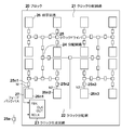
図5は、本実施例に係るクロック分配回路の一例を示す概略ブロック図である。クロック分配回路31aは、半導体集積回路内に設けられ、第1のリファレンスクロック信号として外部のクロック信号の周波数および位相を参照信号として生成されたクロック信号を、複数の順序回路36へ分配する。ここで、順序回路36aと順序回路36bはデータ転送のため接続されている。データ転送パス38は、異ドメイン間データ転送パスを構成している。
FIG. 5 is a schematic block diagram illustrating an example of a clock distribution circuit according to the present embodiment. The clock distribution circuit 31 a is provided in the semiconductor integrated circuit, and distributes a clock signal generated using the frequency and phase of an external clock signal as a first reference clock signal as a reference signal to a plurality of
クロック分配回路31aは、クロック分配網32aと、PLLなどのクロック生成回路33aと、分配回路34、クロックドライバ35と、配線とを具備する。第1フィードバック信号用の分岐点として、クロック分配網の最終段のクロックドライバのうち、クロック生成回路近傍にあるクロックドライバに分岐点NA2を設ける。
The clock distribution circuit 31 a includes a
ここで、第1フィードバック信号用の分岐点は、クロック分配網の最終段のクロックドライバのうち、クロック生成回路33a近傍にあるクロックドライバ35na1の出力の端子側の位置に設定される。よって、フィードバックパス37aは実際の回路レイアウトで製造バラツキによるタイミングのズレが設計マージンに収まるように構成される。フィードバックパス37aは、クロック生成回路33a近傍にあるクロックドライバ35na1の出力端子側から得るため、基本的には配線のみで構成することができ、遅延バラツキを生じさせる構成要素を最小限に抑えることができる。そのため分岐点NA2からリーフの順序回路36aの間の遅延時間と分岐点NA2からクロック生成回路33aの間の遅延時間を合わせることができ、位相調整の精度を向上することができる。なお、図5ではフィードバックパス37aが配線のみで構成されているが、設計マージン内に収まるならばクロックドライバが挿入されていても構わない。また設計マージン内に収まるようにフィードバック分岐点NA2に対してクロック生成回路33aが近くに来るように配置させるような構成であってもよい。
Here, the branch point for the first feedback signal is set to a position on the terminal side of the output of the clock driver 35na1 in the vicinity of the
したがって、分岐点NA2までの同一のクロック分配パスによって分配されたクロック信号が、分岐点NA2を設けた順序回路36aのクロック入力と、クロック生成回路33aのFBK端子とに、分岐点NA2からの分配遅延がほぼ等しくなるように分配される。このため、クロック生成回路のFBK端子でのクロック信号は、順序回路36aのクロック入力のクロック信号と同じ周波数であり、ほぼ位相が等しく位相調整を正しく行うことができる。
Therefore, the clock signal distributed by the same clock distribution path to the branch point NA 2 is a clock input of the
クロック生成回路33bは、第2フィードバック信号を、第2リファレンスクロック信号に同期するように周波数および位相を変調し、第2クロック信号としてクロック分配網32bに出力する。ここで、第2リファレンスクロック信号は、外部からクロックドライバ35bおよび配線を介して、クロック生成回路33bのリファレンスクロック端子RCLKに供給される外部クロック信号である。ここでは、第2リファレンスクロック信号は、第1リファレンスクロック信号と同一である。第2フィードバック信号は、第2フィードバック分岐点NB2からフィードバックパス37bの配線を介して、クロック生成回路33bのフィードバッククロック端子FBKに供給される第2クロック信号である。
The
ブロック30aの接続される順序回路36のうちの順序回路36aと、ブロック30bの接続される順序回路36のうちの順序回路36bとは、データ転送パス38で接続されている。すなわち、順序回路36aと順序回路36bとの間にデータの授受があるため、両者に供給されるクロック信号の位相が揃っている必要がある。そのため、分岐点はデータ転送パスを有する順序回路36a,36bのクロック生成回路33a,33b近傍にあるクロックドライバ35na1,35nb1の出力端子側にそれぞれ設定される。図5ではクロック分配網32aにおける第1フィードバック分岐点NA2をクロックドライバ35na1の出力端子から順序回路36aのクロック入力端子までの間に設ける。同様にクロック分配網32bにおける第2フィードバック分岐点NB2をクロックドライバ35nb1の出力端子から順序回路36bのクロック入力端子までの間に設ける。第1フィードバック信号は順序回路36aのクロック入力のクロック信号とほぼ位相が等しくなる。クロック生成回路33aに第1フィードバック信号と第1リファレンスクロック信号が入力され、クロック生成回路内の位相比較器で位相差が0となるようにクロック生成回路33aは第1クロックを出力する。同様に第2フィードバック信号は順序回路36bのクロック入力のクロック信号とほぼ位相が等しくなる。クロック生成回路33bに第2フィードバック信号と第2リファレンスクロック信号が入力され、クロック生成回路内の位相比較器で位相差が0となるようにクロック生成回路33bは第2クロックを出力する。そしてクロック生成回路33a,33bには同じ位相のリファレンスクロック信号が入力されさえすれば、クロック生成回路33aのFBK端子における第1クロックとクロック生成回路33bのFBK端子における第2クロックとは同じ位相となる。したがって、順序回路36aでの第1クロック信号の位相と順序回路36bでの第2クロック信号の位相とを概ね合わせることができる。その結果、順序回路36aと順序回路36bとの間のデータ転送のタイミングが合い、データ転送に悪影響を与えることなく、異ドメイン間の位相調整の精度を向上することができる。
The
ここで、製造工程に起因する遅延のバラツキを考える。クロック生成回路33aのCLKOUTから順序回路36aのクロック入力までの分配遅延、およびクロック生成回路33aのCLKOUTからクロック生成回路33aのFBK端子までの遅延はバラツキの影響を受ける。しかし、クロック生成回路33aのCLKOUTから分岐点NA2までを共用する構成となっているため、共用部分のバラツキは正確にクロック生成回路33aの位相調整に反映することができる。製造工程に起因する遅延の実質的な影響は、分岐点NA2から順序回路36aのクロック入力までの配線による遅延と分岐点NA2からクロック生成回路33aのFBK端子までの配線による遅延の差分となる。フィードバックパス内にクロックドライバが構成されず、配線を短く構成できるためバラツキの影響を減少させることができる。このことは、クロック分配網32bについても同様である。したがって、順序回路36aから順序回路36bのデータ転送パスにおいて、製造工程に起因したバラツキに影響を抑え、精度の高い位相調整の行うことのできるクロック分配回路を構成できる。
Here, variation in delay due to the manufacturing process is considered. The distribution delay from CLKOUT of the
なお、順序回路36a,36bはFF、レジスタのほかに、クロックによって同期して出力する回路であればよい。また、クロック生成回路33a,33bから分岐点NA2,NB2までは、分岐点なしに複数のバッファを介して分岐点NA2,NB2に接続される構成であってもよい。
The
本発明のクロック分配回路では、図3に示すようにフィードバックパスの分岐点をクロック生成回路の近傍にあるクロックドライバの出力端子側からフィードバックパスを設けることで、バラツキが生じる構成要素を最小に抑え、正しく位相調整を行うことができる。 In the clock distribution circuit of the present invention, as shown in FIG. 3, the feedback path branch point is provided from the output terminal side of the clock driver in the vicinity of the clock generation circuit , thereby minimizing the components that cause variations. Correct phase adjustment can be performed.
Claims (5)
クロック信号を生成するクロック生成回路と、
前記クロック信号が分配されるクロック分配網と、
前記クロック分配網の分岐点を通じて分配されるクロック信号で動作する順序回路とを有し、
前記クロック生成回路は、前記分岐点から分岐した前記クロック信号をフィードバック信号として入力し、該入力したフィードバック信号とリファレンスクロック信号とに基づいて、前記クロック信号を前記クロック分配網へ出力するように構成され、
前記分岐点は、前記クロック分配網の順序回路の前段のクロックドライバのうち、前記クロック生成回路の近傍にあるクロックドライバに設けられる
ことを特徴とするクロック分配回路。 A clock distribution circuit of a semiconductor integrated circuit,
A clock generation circuit for generating a clock signal ;
A clock distribution network before Symbol clock signal is distributed,
Possess a sequential circuit that operates at a clock signal that is distributed through the branch point before Symbol clock distribution network,
The clock generation circuit, the said clock signal branched from the branch point to the input as a feedback signal, based on the feedback signal and the reference clock signal said input, constituting the clock signal so as to output to the clock distribution network And
The clock distribution circuit, wherein the branch point is provided in a clock driver in the vicinity of the clock generation circuit among clock drivers in a preceding stage of the sequential circuit of the clock distribution network.
Priority Applications (2)
| Application Number | Priority Date | Filing Date | Title |
|---|---|---|---|
| JP2012172302A JP2013102417A (en) | 2011-10-14 | 2012-08-02 | Clock distribution circuit |
| US13/597,366 US8710892B2 (en) | 2011-10-14 | 2012-08-29 | Clock distribution circuit |
Applications Claiming Priority (3)
| Application Number | Priority Date | Filing Date | Title |
|---|---|---|---|
| JP2011227436 | 2011-10-14 | ||
| JP2011227436 | 2011-10-14 | ||
| JP2012172302A JP2013102417A (en) | 2011-10-14 | 2012-08-02 | Clock distribution circuit |
Publications (2)
| Publication Number | Publication Date |
|---|---|
| JP2013102417A JP2013102417A (en) | 2013-05-23 |
| JP2013102417A5 true JP2013102417A5 (en) | 2015-08-06 |
Family
ID=48085584
Family Applications (1)
| Application Number | Title | Priority Date | Filing Date |
|---|---|---|---|
| JP2012172302A Pending JP2013102417A (en) | 2011-10-14 | 2012-08-02 | Clock distribution circuit |
Country Status (2)
| Country | Link |
|---|---|
| US (1) | US8710892B2 (en) |
| JP (1) | JP2013102417A (en) |
Families Citing this family (2)
| Publication number | Priority date | Publication date | Assignee | Title |
|---|---|---|---|---|
| US9793900B1 (en) | 2016-06-29 | 2017-10-17 | Microsoft Technology Licensing, Llc | Distributed multi-phase clock generator having coupled delay-locked loops |
| US10585449B1 (en) * | 2019-01-15 | 2020-03-10 | Arm Limited | Clock circuitry for functionally safe systems |
Family Cites Families (7)
| Publication number | Priority date | Publication date | Assignee | Title |
|---|---|---|---|---|
| JPH06282350A (en) * | 1993-01-27 | 1994-10-07 | Hitachi Ltd | Intra-lsi clock distributing circuit |
| US6429715B1 (en) * | 2000-01-13 | 2002-08-06 | Xilinx, Inc. | Deskewing clock signals for off-chip devices |
| JP2002023886A (en) * | 2000-07-11 | 2002-01-25 | Nec Corp | Semiconductor integrated circuit |
| US6809606B2 (en) * | 2002-05-02 | 2004-10-26 | Intel Corporation | Voltage ID based frequency control for clock generating circuit |
| US6839301B2 (en) * | 2003-04-28 | 2005-01-04 | Micron Technology, Inc. | Method and apparatus for improving stability and lock time for synchronous circuits |
| JP2007336003A (en) * | 2006-06-12 | 2007-12-27 | Nec Electronics Corp | Clock distribution circuit, forming method thereof, semiconductor integrated circuit, and program thereof |
| JP2008010607A (en) | 2006-06-29 | 2008-01-17 | Nec Computertechno Ltd | Semiconductor integrated circuit, and clock skew reduction method |
-
2012
- 2012-08-02 JP JP2012172302A patent/JP2013102417A/en active Pending
- 2012-08-29 US US13/597,366 patent/US8710892B2/en active Active
Similar Documents
| Publication | Publication Date | Title |
|---|---|---|
| US9030242B2 (en) | Data output timing control circuit for semiconductor apparatus | |
| KR100853462B1 (en) | Semiconductor memory device | |
| US8674736B2 (en) | Clock synchronization circuit | |
| US9490787B1 (en) | System and method for integrated circuit clock distribution | |
| US8782459B2 (en) | Apparatus and method for advanced synchronous strobe transmission | |
| KR101995389B1 (en) | Phase mixing circuit, semiconductor apparatus and semiconductor system including the same | |
| US9553595B2 (en) | Clock operation method and circuit | |
| JP2011044795A (en) | Input interface circuit | |
| JP7090413B2 (en) | Digital-to-analog converter and its calibration method | |
| US9898035B2 (en) | Clock synchronization method | |
| US20120331330A1 (en) | Programmable mechanism for optimizing a synchronous data bus | |
| US8683253B2 (en) | Optimized synchronous strobe transmission mechanism | |
| US8751851B2 (en) | Programmable mechanism for synchronous strobe advance | |
| KR20130032505A (en) | Semiconductor system | |
| US8782460B2 (en) | Apparatus and method for delayed synchronous data reception | |
| JP2013102417A5 (en) | ||
| Ke et al. | Die-to-die clock synchronization for 3-D IC using dual locking mechanism | |
| US8710892B2 (en) | Clock distribution circuit | |
| US8751850B2 (en) | Optimized synchronous data reception mechanism | |
| US8751852B2 (en) | Programmable mechanism for delayed synchronous data reception | |
| KR100546320B1 (en) | Clock tree synthesis apparatus and method | |
| KR100808592B1 (en) | A circuit for delay locked loop | |
| KR20040072083A (en) | Multi-phase clock generation circuit and method for reducing skew of clock signal | |
| JP2009187110A (en) | Design method for clock distributing circuit | |
| JP2005348168A (en) | Clock control device |