JP2013068793A5 - - Google Patents
Download PDFInfo
- Publication number
- JP2013068793A5 JP2013068793A5 JP2011207141A JP2011207141A JP2013068793A5 JP 2013068793 A5 JP2013068793 A5 JP 2013068793A5 JP 2011207141 A JP2011207141 A JP 2011207141A JP 2011207141 A JP2011207141 A JP 2011207141A JP 2013068793 A5 JP2013068793 A5 JP 2013068793A5
- Authority
- JP
- Japan
- Prior art keywords
- unit
- driving
- address information
- display
- period
- Prior art date
- Legal status (The legal status is an assumption and is not a legal conclusion. Google has not performed a legal analysis and makes no representation as to the accuracy of the status listed.)
- Abandoned
Links
- 238000000034 method Methods 0.000 claims description 3
- 238000006243 chemical reaction Methods 0.000 description 4
- 230000001360 synchronised effect Effects 0.000 description 1
Images
Description
本開示の駆動方法は、複数の表示画素を含む表示部における、駆動すべき水平ラインを指定するためのアドレス情報を生成し、アドレス情報により指定された水平ラインを駆動するために設定された単位駆動期間内に、複数ビットからなる階調コードの各ビットの重みに応じた駆動間隔で、各ビットの値に応じて表示画素を駆動し、単位駆動期間の開始タイミングを任意に設定するものである。 The driving method of the present disclosure, the display unit including a plurality of display pixels, generates address information for designating the horizontal line to be driven, is set to drive the designated horizontal line by address information A display pixel is driven according to the value of each bit at a driving interval corresponding to the weight of each bit of a gradation code consisting of a plurality of bits within a unit driving period, and the start timing of the unit driving period is arbitrarily set It is.
コントローラ21は、同期信号Ssyncに基づいて、変換回路30、水平駆動回路23、および垂直駆動回路22に対してそれぞれ制御信号を供給し、これらがお互いに同期して動作するように制御する回路である。具体的には、コントローラ21は、変換回路30に対して制御信号CTLAを供給し、水平駆動回路23に対して制御信号CTLBを供給し、垂直駆動回路22に対して制御信号CTLCを供給する。制御信号CTLA,CTLB,CTLCとしては、例えば、クロック信号CLK、ラッチ信号、フレーム開始信号などが挙げられる。 The controller 21 is a circuit that supplies control signals to the conversion circuit 30, the horizontal drive circuit 23, and the vertical drive circuit 22 based on the synchronization signal Ssync, and controls them to operate in synchronization with each other. is there. Specifically, the controller 21 supplies a control signal CTLA to the conversion circuit 30, supplies a control signal CTLB to the horizontal drive circuit 23 , and supplies a control signal CTLC to the vertical drive circuit 22 . Examples of the control signals CTLA, CTLB, and CTLC include a clock signal CLK, a latch signal, and a frame start signal.
(全体動作概要)
まず、図1を参照して、立体表示装置1の全体動作概要を説明する。コントローラ24は、同期信号Ssyncに基づいて、変換回路30、水平駆動回路23、および垂直駆動回路22の動作タイミングを制御する制御信号CTLA,CTLB,CTLCをそれぞれ生成するとともに、表示パネル10における、階調コードCに基づく書込み動作を行う行を設定し、それに基づいてアドレス信号ADRを生成する。変換回路30は、同期信号Ssyncに同期した映像信号Sdispを映像信号Sigに変換する。垂直駆動回路22は、制御信号CTLCおよびアドレス信号ADRに基づいて、走査線信号WSを生成する。水平駆動回路23は、制御信号CTLBおよび信号データSigに基づいて、データ線信号DTを生成する。表示パネル10の各画素11は、データ線信号DTおよび走査線信号WSに基づいて、パルス幅変調により階調表示を行う。
(Overview of overall operation)
First, with reference to FIG. 1, an overview of the overall operation of the stereoscopic display device 1 will be described. The controller 24 generates control signals CTLA, CTLB, CTLC for controlling the operation timings of the conversion circuit 30, the horizontal drive circuit 23, and the vertical drive circuit 22 based on the synchronization signal Ssync, respectively. A row for performing a write operation based on the key code C is set, and an address signal ADR is generated based on the row. The conversion circuit 30 converts the video signal Sdisp synchronized with the synchronization signal Ssync into a video signal Sig. The vertical drive circuit 22 generates the scanning line signal WS based on the control signal CTLC and the address signal ADR. The horizontal drive circuit 23 generates a data line signal DT based on the control signal CTLB and the signal data Sig. Each pixel 11 of the display panel 10 performs gradation display by pulse width modulation based on the data line signal DT and the scanning line signal WS.
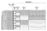
次に、サブフレームSF2内の2番目の水平期間において、同様に、水平駆動回路23が、階調コードCのビットb2に対応する電圧をデータ線DTLに印加するとともに、垂直駆動回路22が、1行目の走査線WSL(1)に走査パルスを印加する(図4(A))。これにより、1行目の画素11には、ビットb2の値が書き込まれ、この画素11は、次に書き込まれるまでの期間(ビットプレーンBP2)、その値を維持する(図4(B))。 Next, in the second horizontal period in the subframe SF2, similarly, the horizontal drive circuit 23 applies a voltage corresponding to the bit b2 of the gradation code C to the data line DTL, and the vertical drive circuit 22 A scan pulse is applied to the scan line WSL (1) in the first row (FIG. 4A). As a result, the value of bit b2 is written to the pixel 11 in the first row, and this pixel 11 maintains that value until the next writing (bit plane BP2) (FIG. 4B). .
次に、サブフレームSF4内の3番目の水平期間において、水平駆動回路23が、階調コードCのビットb3に対応する電圧をデータ線DTLに印加するとともに、垂直駆動回路22が、1行目の走査線WSL(1)に走査パルスを印加する(図4(A))。これにより、1行目の画素11には、ビットb3の値が書き込まれ、この画素11は、次に書き込まれるまでの期間(ビットプレーンBP3)、その値を維持する(図4(B))。 Next, in the third horizontal period in the subframe SF4, the horizontal drive circuit 23 applies a voltage corresponding to the bit b3 of the gradation code C to the data line DTL, and the vertical drive circuit 22 performs the first row. A scan pulse is applied to the scan line WSL (1) (FIG. 4A). As a result, the value of bit b3 is written to the pixel 11 in the first row, and this pixel 11 maintains that value until the next writing (bit plane BP3) (FIG. 4B). .
(16)複数の表示画素を含む表示部における、駆動すべき水平ラインを指定するためのアドレス情報を生成し、
前記アドレス情報により指定された水平ラインを駆動するために設定された単位駆動期
間内に、複数ビットからなる階調コードの各ビットの重みに応じた駆動間隔で、各ビット
の値に応じて表示画素を駆動し、
前記単位駆動期間の開始タイミングを任意に設定する
駆動方法。
(16) generating address information for designating a horizontal line to be driven in a display unit including a plurality of display pixels;
Display the the set unit within the driving period for driving a designated horizontal line by the address information, the driving interval corresponding to weight of each bit of the gray scale code of a plurality of bits, depending on the value of each bit Drive the pixel,
A driving method for arbitrarily setting a start timing of the unit driving period.
Claims (17)
駆動すべき水平ラインを指示するためのアドレス情報を生成する制御部と、
前記アドレス情報により指定された水平ラインを駆動するために設定された単位駆動期間内に、複数ビットからなる階調コードの各ビットの重みに応じた駆動間隔で、各ビットの値に応じて表示画素を駆動する駆動部と
を備え、
前記制御部は、前記単位駆動期間の開始タイミングを任意に設定する
表示装置。 A display unit including a plurality of display pixels;
A control unit for generating address information for indicating a horizontal line to be driven;
Displayed according to the value of each bit at a driving interval corresponding to the weight of each bit of the gradation code consisting of a plurality of bits within a unit driving period set to drive the horizontal line specified by the address information A drive unit for driving the pixels,
The control unit arbitrarily sets a start timing of the unit drive period.
請求項1に記載の表示装置。 The display device according to claim 1, wherein the control unit sets a start timing so as to start the unit drive periods in an order different from an arrangement order of horizontal lines in the display unit.
前記制御部は、前記サブフレーム期間を単位として、前記開始タイミングを設定する
請求項2に記載の表示装置。 Each frame period includes a plurality of subframe periods having equal time widths,
The display device according to claim 2, wherein the control unit sets the start timing in units of the subframe period.
前記駆動部は、前記水平期間を単位として、前記表示画素を駆動する
請求項3に記載の表示装置。 Each subframe period is divided into a plurality of horizontal periods having equal time widths,
The display device according to claim 3, wherein the driving unit drives the display pixel in units of the horizontal period.
請求項4に記載の表示装置。 The display device according to claim 4, wherein the control unit supplies the address information to the driving unit for each horizontal period.
請求項5に記載の表示装置。 The display device according to claim 5, wherein the control unit supplies address information of a horizontal line to be driven in a next horizontal period to the driving unit.
請求項5に記載の表示装置。 The display device according to claim 5, wherein the control unit generates address information of a horizontal line to be driven in a current horizontal period.
請求項1から請求項7のいずれか一項に記載の表示装置。 The display device according to any one of claims 1 to 7, wherein the control unit outputs the address information as a serial signal.
請求項4から請求項7のいずれか一項に記載の表示装置。 Wherein the control unit outputs the respective bits of the tone codes as a parallel signal bus having a predetermined bit width, claim claim 4 for outputting the address information in at least a portion of the bus as a parallel signal display device according to any one of 7.
請求項9に記載の表示装置。 The display device according to claim 9, wherein the control unit arranges the address information before each bit of the gradation code in each horizontal period.
前記アドレス情報に基づいて、駆動すべき水平ラインを選択する走査駆動部と、
前記階調コードの各ビットの値に対応した電圧を表示画素に供給する表示駆動部と、
を有し、
前記制御部は、前記階調コードおよび前記アドレス情報を前記表示駆動部に供給し、
前記表示駆動部は、前記アドレス情報を前記走査駆動部に供給する
請求項9または請求項10に記載の表示装置。 The drive unit is
A scan driver that selects a horizontal line to be driven based on the address information;
A display driver for supplying a voltage corresponding to the value of each bit of the gradation code to a display pixel;
Have
The control unit supplies the gradation code and the address information to the display driving unit,
The display device according to claim 9, wherein the display driving unit supplies the address information to the scan driving unit.
請求項4から請求項11のいずれか一項に記載の表示装置。 The display device according to any one of claims 4 to 11, wherein the control unit supplies the address information of the predetermined number of horizontal lines to the driving unit every a plurality of predetermined number of horizontal periods. .
請求項4から請求項11のいずれか一項に記載の表示装置。 The display device according to claim 4, wherein the control unit supplies the address information of a plurality of horizontal lines to the driving unit for each horizontal period.
請求項1から請求項13のいずれか一項に記載の表示装置。 The display device according to any one of claims 1 to 13, wherein a time of the unit drive period is equal to a time of one frame period.
前記アドレス情報により指定された水平ラインを駆動するために設定された単位駆動期間内に、複数ビットからなる階調コードの各ビットの重みに応じた駆動間隔で、各ビットの値に応じて表示画素を駆動する駆動部と
を備え、
前記制御部は、前記単位駆動期間の開始タイミングを任意に設定する
駆動回路。 A control unit for generating address information for designating a horizontal line to be driven in a display unit including a plurality of display pixels;
Displayed according to the value of each bit at a driving interval corresponding to the weight of each bit of the gradation code consisting of a plurality of bits within a unit driving period set to drive the horizontal line specified by the address information A drive unit for driving the pixels,
The control unit arbitrarily sets a start timing of the unit drive period.
前記アドレス情報により指定された水平ラインを駆動するために設定された単位駆動期間内に、複数ビットからなる階調コードの各ビットの重みに応じた駆動間隔で、各ビットの値に応じて表示画素を駆動し、
前記単位駆動期間の開始タイミングを任意に設定する
駆動方法。 Generating address information for designating a horizontal line to be driven in a display unit including a plurality of display pixels;
I display the the set unit within the driving period for driving a designated horizontal line by the address information, the driving interval corresponding to weight of each bit of the gray scale code of a plurality of bits, depending on the value of each bit Drive the pixel,
A driving method for arbitrarily setting a start timing of the unit driving period.
前記表示装置を利用した動作制御を行う制御部と
を備え、
前記表示装置は、
複数の表示画素を含む表示部と、
駆動すべき水平ラインを指示するためのアドレス情報を生成する制御部と、
前記アドレス情報により指定された水平ラインを駆動するために設定された単位駆動期間内に、複数ビットからなる階調コードの各ビットの重みに応じた駆動間隔で、各ビットの値に応じて表示画素を駆動する駆動部と
を有し、
前記制御部は、前記単位駆動期間の開始タイミングを任意に設定する
電子機器。 A display device;
A control unit that performs operation control using the display device,
The display device
A display unit including a plurality of display pixels;
A control unit for generating address information for indicating a horizontal line to be driven;
Displayed according to the value of each bit at a driving interval corresponding to the weight of each bit of the gradation code consisting of a plurality of bits within a unit driving period set to drive the horizontal line specified by the address information A drive unit for driving the pixels,
The said control part is an electronic device which sets the start timing of the said unit drive period arbitrarily.
Priority Applications (3)
| Application Number | Priority Date | Filing Date | Title |
|---|---|---|---|
| JP2011207141A JP2013068793A (en) | 2011-09-22 | 2011-09-22 | Display device, drive circuit, driving method, and electronic system |
| US13/612,060 US20130076802A1 (en) | 2011-09-22 | 2012-09-12 | Display device, drive circuit, driving method, and electronic system |
| CN2012103432718A CN103021310A (en) | 2011-09-22 | 2012-09-14 | Display device, drive circuit, driving method, and electronic system |
Applications Claiming Priority (1)
| Application Number | Priority Date | Filing Date | Title |
|---|---|---|---|
| JP2011207141A JP2013068793A (en) | 2011-09-22 | 2011-09-22 | Display device, drive circuit, driving method, and electronic system |
Publications (2)
| Publication Number | Publication Date |
|---|---|
| JP2013068793A JP2013068793A (en) | 2013-04-18 |
| JP2013068793A5 true JP2013068793A5 (en) | 2014-10-02 |
Family
ID=47910819
Family Applications (1)
| Application Number | Title | Priority Date | Filing Date |
|---|---|---|---|
| JP2011207141A Abandoned JP2013068793A (en) | 2011-09-22 | 2011-09-22 | Display device, drive circuit, driving method, and electronic system |
Country Status (3)
| Country | Link |
|---|---|
| US (1) | US20130076802A1 (en) |
| JP (1) | JP2013068793A (en) |
| CN (1) | CN103021310A (en) |
Families Citing this family (7)
| Publication number | Priority date | Publication date | Assignee | Title |
|---|---|---|---|---|
| JP2015125427A (en) * | 2013-12-27 | 2015-07-06 | 三星ディスプレイ株式會社Samsung Display Co.,Ltd. | Drive method of display device and display device |
| TWI616859B (en) * | 2017-05-17 | 2018-03-01 | 友達光電股份有限公司 | Pixel driving method and panel driving circuit |
| CN107481692A (en) * | 2017-09-05 | 2017-12-15 | 珠海格力电器股份有限公司 | The display methods and equipment of a kind of section-type LCD |
| CN111415628A (en) * | 2020-04-26 | 2020-07-14 | Tcl华星光电技术有限公司 | Backlight unit, control method thereof and liquid crystal display device |
| CN112735345B (en) * | 2021-01-08 | 2022-03-08 | Tcl华星光电技术有限公司 | Control method of backlight unit, display panel and display device |
| CN113380200B (en) * | 2021-06-07 | 2023-01-24 | 惠州华星光电显示有限公司 | Display method, display device and mobile terminal |
| CN114677955B (en) * | 2022-03-17 | 2023-09-26 | Tcl华星光电技术有限公司 | Display panel and control method thereof |
Family Cites Families (8)
| Publication number | Priority date | Publication date | Assignee | Title |
|---|---|---|---|---|
| AU617006B2 (en) * | 1988-09-29 | 1991-11-14 | Canon Kabushiki Kaisha | Data processing system and apparatus |
| US5818419A (en) * | 1995-10-31 | 1998-10-06 | Fujitsu Limited | Display device and method for driving the same |
| US6353435B2 (en) * | 1997-04-15 | 2002-03-05 | Hitachi, Ltd | Liquid crystal display control apparatus and liquid crystal display apparatus |
| JP4066662B2 (en) * | 2001-03-09 | 2008-03-26 | セイコーエプソン株式会社 | Electro-optical element driving method, driving apparatus, and electronic apparatus |
| JP4074502B2 (en) * | 2001-12-12 | 2008-04-09 | セイコーエプソン株式会社 | Power supply circuit for display device, display device and electronic device |
| US6788282B2 (en) * | 2002-02-21 | 2004-09-07 | Seiko Epson Corporation | Driving method for electro-optical device, driving circuit therefor, electro-optical device, and electronic apparatus |
| JP5002914B2 (en) * | 2005-06-10 | 2012-08-15 | ソニー株式会社 | Display device and driving method of display device |
| JP2007140379A (en) * | 2005-11-22 | 2007-06-07 | Toshiba Matsushita Display Technology Co Ltd | Display device and driving method of display device |
-
2011
- 2011-09-22 JP JP2011207141A patent/JP2013068793A/en not_active Abandoned
-
2012
- 2012-09-12 US US13/612,060 patent/US20130076802A1/en not_active Abandoned
- 2012-09-14 CN CN2012103432718A patent/CN103021310A/en active Pending
Similar Documents
| Publication | Publication Date | Title |
|---|---|---|
| JP2013068793A5 (en) | ||
| US8810479B2 (en) | Multi-panel display device configured to align multiple flat panel display devices for representing a single image and method of driving the same | |
| KR101354427B1 (en) | Display device and Methode of driving the same | |
| WO2015176511A1 (en) | Touch display screen and time-sharing drive method thereof | |
| US10074327B2 (en) | Display apparatus and method of driving the same | |
| JP2007226180A5 (en) | ||
| JP2010191038A5 (en) | ||
| JP2008256954A5 (en) | ||
| JP2009520223A5 (en) | ||
| US20130076802A1 (en) | Display device, drive circuit, driving method, and electronic system | |
| CN101025899A (en) | Source driving apparatus, method of driving the same, display device and method of driving the same | |
| JP2007226226A5 (en) | ||
| CN105321476B (en) | Drive method, light source equipment and the display equipment with the light source equipment of light source | |
| JP2005181743A5 (en) | ||
| US20140368478A1 (en) | Electronic apparatus and associated frame updating method | |
| JP2012098608A (en) | Matrix display device and method for driving the same | |
| US20120200553A1 (en) | Multiple polarity inversion driving method and display driver, timing controller, and display device using the same | |
| JP5672468B2 (en) | Display device and driving method thereof | |
| JP2009037028A (en) | Display device and method for changing display mode | |
| KR20150113266A (en) | Display device | |
| TW200630935A (en) | Driving circuit and method for data drivers in a bi-stable display | |
| JP2000261739A (en) | Driver for plasma display device | |
| US20070121395A1 (en) | Device and Method of Controlling Source Driver | |
| KR102536726B1 (en) | Flat display device and method for driving the same | |
| JP2009015103A (en) | Display controller and its control method |