JP2013003166A - Information indicator and information indication system - Google Patents

Information indicator and information indication system Download PDF

Info

Publication number
JP2013003166A
JP2013003166A JP2011130592A JP2011130592A JP2013003166A JP 2013003166 A JP2013003166 A JP 2013003166A JP 2011130592 A JP2011130592 A JP 2011130592A JP 2011130592 A JP2011130592 A JP 2011130592A JP 2013003166 A JP2013003166 A JP 2013003166A
Authority
JP
Japan
Prior art keywords
information
information display
display
control device
control signal
Prior art date
Legal status (The legal status is an assumption and is not a legal conclusion. Google has not performed a legal analysis and makes no representation as to the accuracy of the status listed.)
Withdrawn
Application number
JP2011130592A
Other languages
Japanese (ja)
Inventor
Akihiko Yokoo
彰彦 横尾
Hirotaka Yamazaki
博貴 山▲崎▼
Norio Nihei
則夫 二瓶
Current Assignee (The listed assignees may be inaccurate. Google has not performed a legal analysis and makes no representation or warranty as to the accuracy of the list.)
Bridgestone Corp
Original Assignee
Bridgestone Corp
Priority date (The priority date is an assumption and is not a legal conclusion. Google has not performed a legal analysis and makes no representation as to the accuracy of the date listed.)
Filing date
Publication date
Application filed by Bridgestone Corp filed Critical Bridgestone Corp
Priority to JP2011130592A priority Critical patent/JP2013003166A/en
Priority to PCT/JP2012/064704 priority patent/WO2012169594A1/en
Publication of JP2013003166A publication Critical patent/JP2013003166A/en
Withdrawn legal-status Critical Current

Links

Images

Landscapes

  • Control Of Indicators Other Than Cathode Ray Tubes (AREA)
  • Devices For Indicating Variable Information By Combining Individual Elements (AREA)

Abstract

PROBLEM TO BE SOLVED: To individually discriminate a plurality of information indicators bound like a booklet and to indicate predetermined information on the discriminated corresponding information indicator.SOLUTION: An information indicator 110 includes a connection mechanism connected to a control device. The connection mechanism includes a conductive part electrically connected to the control device and an insulated part electrically insulated from the control device. A control signal receiving part for receiving a control signal is formed on the conductive part. The information indicator 110 includes also a determination circuit configured so as to determine whether indicated information of the information indicator itself is to be rewritten or not based on an arrangement pattern of the conductive part and the insulated part and the control signal received by the control signal receiving part.

Description

本発明は、複数の表示用電極と、複数の表示用電極の間に配置され、且つ表示用電極間に印加された電圧によって駆動される表示媒体とを有する情報表示器、及び複数の情報表示器が一纏めに綴られた冊子型の情報表示システムに関する。   The present invention relates to an information display having a plurality of display electrodes and a display medium disposed between the plurality of display electrodes and driven by a voltage applied between the display electrodes, and a plurality of information displays The present invention relates to a booklet-type information display system in which containers are spelled together.

従来、少なくとも観察側となる基板が透明な2枚の基板を対向させて形成した空間に、電気的に駆動できる表示媒体を配置した情報表示パネルが情報表示器として知られている。   2. Description of the Related Art Conventionally, an information display panel is known as an information display device in which a display medium that can be electrically driven is arranged in a space formed by facing two substrates that are transparent at least on the observation side.

更に、紙と同様に、複数の情報表示器を見開き可能に綴った情報表示装置が開示されている(例えば、特許文献1参照)。このような情報表示装置によれば、情報表示器を冊子のように利用することができる。   Furthermore, an information display device is disclosed in which a plurality of information displays are spread like a paper (see, for example, Patent Document 1). According to such an information display device, the information display can be used like a booklet.

特開2006−162902号公報JP 2006-162902 A

ところが、特許文献1に記載された情報表示装置では、次のような問題点があった。すなわち、情報表示装置の各情報表示器を一度見開きにしなければ、本体に認識されず、各情報表示器に表示させる情報の書き換えを行うことができなかった。   However, the information display device described in Patent Document 1 has the following problems. That is, unless each information display of the information display device is spread once, it is not recognized by the main body, and the information displayed on each information display cannot be rewritten.

そこで、本発明は、このような状況に鑑みてなされたものであり、複数の情報表示器を冊子状に綴った状態で個別に識別可能で、且つ該当する情報表示器に所定の情報を表示させることができる情報表示器、及び情報表示システムを提供することを目的とする。   Therefore, the present invention has been made in view of such a situation, and a plurality of information displays can be individually identified in a booklet form, and predetermined information is displayed on the corresponding information display. It is an object of the present invention to provide an information display device and an information display system that can be used.

上述した課題を解決するため、本発明の特徴は、少なくとも一方の基板が透明な情報表示領域を備える2つの基板と、前記2つの基板の間に対向して配置された複数の表示用電極と、複数の前記表示用電極間に配置されており前記表示用電極間に印加した電圧によって駆動される表示媒体と、前記表示用電極と電気的に接続されており制御装置から送信される制御信号によって前記情報表示領域に情報を表示するように前記表示用電極間に電圧を印加する駆動回路と、前記制御装置と連結される連結機構とを有する情報表示器であって、前記連結機構は、前記制御装置と電気的に接続される導通部分と、前記制御装置と電気的に絶縁された絶縁部分と、を有し、前記導通部分には、前記制御信号を受信する制御信号受信部が形成されており、前記導通部分と前記絶縁部分との配置パターンと、前記制御信号受信部によって受信した制御信号とに基づいて、当該情報表示器自身の表示情報を書き換えるか書き換えないかを決定するように構成された判定回路を有することを要旨とする。   In order to solve the above-described problem, the present invention is characterized in that at least one of the substrates includes a transparent information display region, and a plurality of display electrodes arranged to face each other between the two substrates. A display medium disposed between the plurality of display electrodes and driven by a voltage applied between the display electrodes, and a control signal electrically connected to the display electrodes and transmitted from a control device The information display device includes a drive circuit that applies a voltage between the display electrodes so as to display information in the information display area, and a connection mechanism that is connected to the control device. A conductive portion electrically connected to the control device; and an insulating portion electrically insulated from the control device; and a control signal receiving portion for receiving the control signal is formed in the conductive portion. Has been Based on the arrangement pattern of the conductive portion and the insulating portion and the control signal received by the control signal receiving unit, it is configured to determine whether or not to rewrite the display information of the information display itself. The gist is to have a determination circuit.

本発明の特徴によれば、情報表示器が備える判定回路が、導通部分と絶縁部分との配置パターンと、制御信号受信部によって受信した制御信号とに基づいて、その情報表示器の表示情報を書き換えるか書き換えないかを決定する。このため、制御装置は、導通部分と絶縁部分との配置パターンと、制御装置が送信した制御信号とに基づいて、特定した所定の情報表示器に情報を表示させる処理を行わせることができる。   According to the feature of the present invention, the determination circuit included in the information display device displays the display information of the information display device based on the arrangement pattern of the conductive portion and the insulating portion and the control signal received by the control signal receiving unit. Decide whether to rewrite or not. For this reason, the control device can perform a process of displaying information on the specified predetermined information display device based on the arrangement pattern of the conductive portion and the insulating portion and the control signal transmitted by the control device.

また、本発明の特徴によれば、制御装置に連結される全ての情報表示器の駆動回路に向けて制御信号を送信し、表示情報を書き換えることになった情報表示器のみにおいて書き換えを実行することができる。これにより、制御装置と複数の情報表示器との電気的な接続部を共通化できる。従って、1台の制御装置と複数の情報表示器とを連結する連結機構に電気的な接続部を設けて、複数の情報表示器を綴じた構造の冊子を形成することができる。   Further, according to the feature of the present invention, the control signal is transmitted to the drive circuits of all the information display devices connected to the control device, and the rewriting is executed only in the information display device in which the display information is to be rewritten. be able to. Thereby, the electrical connection part of a control apparatus and a some information indicator can be shared. Therefore, it is possible to form a booklet having a structure in which a plurality of information displays are bound by providing an electrical connection portion in a coupling mechanism that connects one control device and a plurality of information displays.

本発明に係る情報表示システムは、複数の情報表示器と、複数の前記情報表示器に情報を表示するように制御する制御装置と、を備え、前記情報表示器の各々は、少なくとも一方の基板が透明な情報表示領域を備える2つの基板と、前記2つの基板の間に対向して配置された複数の表示用電極と、複数の前記表示用電極間に配置されており前記表示用電極間に印加された電圧によって駆動される表示媒体と、前記表示用電極と電気的に接続されており制御装置から送信される制御信号によって前記情報表示領域に情報を表示するように前記表示用電極間に電圧を印加する駆動回路と、を備え、前記制御装置は、前記情報表示器の各々と連結される制御装置側連結機構を有し、前記制御装置側連結機構には、前記制御信号を送信する制御信号送信部が形成され、前記情報表示器の各々は、前記制御装置と連結される情報表示器側連結機構を有し、前記情報表示器側連結機構は、前記制御装置と電気的に接続される導通部分と、前記制御装置と電気的に絶縁された絶縁部分と、を有し、前記導通部分には、前記制御信号を受信する制御信号受信部が形成されており、前記情報表示器の各々は、前記導通部分と前記絶縁部分との配置パターンと、前記制御信号受信部によって受信した制御信号とに基づいて、当該情報表示器自身の表示情報を書き換えるか書き換えないかを決定するように構成された判定回路を有しており、前記情報表示器側連結機構における前記導通部分と前記絶縁部分の配置パターンは、前記情報表示器毎に異なっていることを要旨とする。   An information display system according to the present invention includes a plurality of information displays and a control device that controls to display information on the plurality of information displays, and each of the information displays includes at least one substrate. Is provided between two display electrodes, a plurality of display electrodes disposed opposite to each other between the two substrates, and a plurality of display electrodes disposed between the two display electrodes. A display medium driven by a voltage applied to the display electrode, and the display electrode electrically connected to the display electrode and displaying information in the information display area by a control signal transmitted from a control device A drive circuit for applying a voltage to the control device, the control device having a control device side connection mechanism connected to each of the information indicators, and transmitting the control signal to the control device side connection mechanism Control signal transmission Each of the information displays has an information display side connection mechanism connected to the control device, and the information display side connection mechanism is electrically connected to the control device. And a control signal receiving unit for receiving the control signal is formed in the conductive part, and each of the information indicators is provided with an insulating part electrically insulated from the control device. The display information of the information display device itself is determined to be rewritten or not to be rewritten based on the arrangement pattern of the conductive portion and the insulating portion and the control signal received by the control signal receiving unit. The determination circuit is provided, and the arrangement pattern of the conductive portion and the insulating portion in the information display side connection mechanism is different for each information display.

本発明によれば、複数の情報表示器を冊子状に綴った状態で個別に識別可能にして、見開いていない状態(綴じられた冊子を閉じている状態)であっても該当する情報表示器に所定の情報を表示させることができる情報表示器および複数の情報表示器で構成される情報表示システムを提供できる。   According to the present invention, a plurality of information indicators can be individually identified in a booklet-like state, and the corresponding information indicator is in an unopened state (a state where the bound booklet is closed). It is possible to provide an information display system including an information display capable of displaying predetermined information and a plurality of information displays.

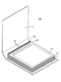
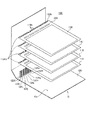
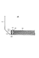
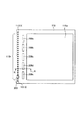
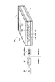
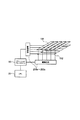
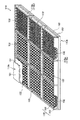
図1は、本発明の実施形態に係る情報表示システムの概略構成を示す斜視図である。FIG. 1 is a perspective view showing a schematic configuration of an information display system according to an embodiment of the present invention. 図2は、本発明の実施形態に係る情報表示システムの分解斜視図である。FIG. 2 is an exploded perspective view of the information display system according to the embodiment of the present invention. 図3は、本発明の実施形態に係る情報表示システムの断面図である。FIG. 3 is a cross-sectional view of the information display system according to the embodiment of the present invention. 図4は、本発明の実施形態に係る情報表示システムの情報表示器を説明する平面図である。FIG. 4 is a plan view for explaining an information display of the information display system according to the embodiment of the present invention. 図5は、図4に示す情報表示器のA−A線における断面図である。FIG. 5 is a cross-sectional view taken along line AA of the information display shown in FIG. 図6は、実施形態に係る情報表示器の判定回路の回路構成を部分的に拡大した部6分拡大図である。FIG. 6 is an enlarged view of a part 6 in which the circuit configuration of the determination circuit of the information display device according to the embodiment is partially enlarged. 図7は、本発明の実施形態に係る情報表示器の断面図である。FIG. 7 is a cross-sectional view of the information display device according to the embodiment of the present invention. 図8は、実施形態に係る情報表示器の孔部の拡大図である。FIG. 8 is an enlarged view of a hole of the information display device according to the embodiment. 図9は、実施形態に係る情報表示器の識別信号受信部の判定回路構成を説明する回路図である。FIG. 9 is a circuit diagram illustrating a determination circuit configuration of the identification signal receiving unit of the information display device according to the embodiment. 図10は、実施形態に係る情報表示器に配置される駆動回路と、駆動回路に接続される接続線を説明する図である。FIG. 10 is a diagram illustrating a drive circuit arranged in the information display device according to the embodiment and a connection line connected to the drive circuit. 図11は、制御装置が複数の情報表示器のうち所定の情報表示器に情報を表示する処理を説明するフローチャートである。FIG. 11 is a flowchart illustrating a process in which the control device displays information on a predetermined information display among a plurality of information displays. 図12は、制御装置側連結機構の変形例を説明する図である。FIG. 12 is a diagram illustrating a modification of the control device side coupling mechanism. 図13は、制御装置側連結機構の変形例を説明する図である。FIG. 13 is a diagram illustrating a modification of the control device side coupling mechanism. 図14は、制御装置側連結機構の変形例を説明する図である。FIG. 14 is a diagram illustrating a modification of the control device side coupling mechanism. 図15は、制御装置側連結機構において電気を導通するための構造の変形例を説明する図である。FIG. 15 is a diagram illustrating a modification of the structure for conducting electricity in the control device side coupling mechanism. 図16は、図15のD−D線における断面図である。16 is a cross-sectional view taken along the line DD of FIG. 図17(a)は、図15,16に示す変形例に対応する孔部を説明する平面図であり、図17(b)は、孔部の変形例を説明する平面図である。FIG. 17A is a plan view illustrating a hole corresponding to the modification shown in FIGS. 15 and 16, and FIG. 17B is a plan view illustrating a modification of the hole. 図18は、本実施形態に係る情報表示システムに適用可能な情報表示器の一例を説明する概略斜視図である。FIG. 18 is a schematic perspective view for explaining an example of an information display applicable to the information display system according to the present embodiment. 図19は、情報表示システムの機能ブロック構成図である。FIG. 19 is a functional block configuration diagram of the information display system. 図20は、情報表示システムに適用可能な情報表示器の一例である粒子移動型の情報表示器の一部を分解して示す分解斜視図である。FIG. 20 is an exploded perspective view showing a part of a particle movement type information display which is an example of an information display applicable to the information display system.

以下、本発明の実施形態に係る情報表示器の一例及び制御装置の一例について、図面を参照しながら説明する。具体的には、(1)情報表示システムの概略構成、(2)情報表示器の概略構成、(3)識別信号受信部の構成、(4)判定回路の回路構成、(5)情報表示器に情報を表示する処理、(6)作用・効果、(7)連結機構の変形例、(8)連結機構の導通構造の変形例、(9)情報表示器の概略構成、(10)その他実施形態について説明する。   Hereinafter, an example of an information display device and an example of a control device according to an embodiment of the present invention will be described with reference to the drawings. Specifically, (1) schematic configuration of information display system, (2) schematic configuration of information display, (3) configuration of identification signal receiver, (4) circuit configuration of determination circuit, (5) information display (6) Action / effect, (7) Modification of coupling mechanism, (8) Modification of conduction structure of coupling mechanism, (9) Schematic configuration of information display, (10) Other implementation A form is demonstrated.

以下の図面の記載において、同一または類似の部分には、同一又は類似の符号を付している。図面は模式的なのものであり、各寸法の比率などは現実のものとは異なることを留意すべきである。具体的な寸法などは、以下の説明を参酌して判断すべきものである。図面相互間においても互いの寸法の関係や比率が異なる部分が含まれていることは勿論である。   In the following description of the drawings, the same or similar parts are denoted by the same or similar reference numerals. It should be noted that the drawings are schematic and ratios of dimensions and the like are different from actual ones. Specific dimensions should be determined in consideration of the following description. It goes without saying that the drawings include parts having different dimensional relationships and ratios.

(1)情報表示システムの概略構成
図1は、情報表示システム100の概略構成を示す斜視図である。図2は、情報表示システム100の分解斜視図である。図3は、情報表示システム100の断面図である。情報表示システム100は、複数の情報表示器110と、複数の情報表示器110に対する情報の表示を制御する制御装置120とを備える。実施形態では、制御装置120は、外装体Cを構成している。制御装置120は、CPU20、グラフィックコントローラ30、メモリなどを備えており、情報表示器110への情報の表示を制御する。
(1) Schematic Configuration of Information Display System FIG. 1 is a perspective view showing a schematic configuration of the information display system 100. FIG. 2 is an exploded perspective view of the information display system 100. FIG. 3 is a cross-sectional view of the information display system 100. The information display system 100 includes a plurality of information displays 110 and a control device 120 that controls display of information on the plurality of information displays 110. In the embodiment, the control device 120 constitutes the exterior body C. The control device 120 includes a CPU 20, a graphic controller 30, a memory, and the like, and controls display of information on the information display 110.

実施形態に係る情報表示システム100では、制御装置120には、外装体Cから突出した複数の突出部121が形成されており、複数の情報表示器110には孔部(貫通孔)110hが形成されている。孔部110hに突出部121が貫通されることにより、情報表示器110が制御装置120に取り付けられる。複数の情報表示器110は、制御装置120に冊子状に綴られている。また、制御装置120には、パーソナルコンピュータ(PC)、その他の電子機器、記憶装置などと接続可能な接続端子が設けられていてもよい(不図示)。   In the information display system 100 according to the embodiment, the control device 120 is formed with a plurality of protrusions 121 protruding from the exterior body C, and the plurality of information displays 110 are formed with holes (through holes) 110h. Has been. The information display device 110 is attached to the control device 120 by the protrusion 121 passing through the hole 110h. The plurality of information displays 110 are spelled into the control device 120 in a booklet form. The control device 120 may be provided with a connection terminal (not shown) that can be connected to a personal computer (PC), other electronic devices, a storage device, and the like.

さらにまた、情報表示を実行する時に必要な電源供給は、外装体Cにシート電池やコイン型電池などの電源を搭載して制御装置120と接続させたり、外装体Cに設けた制御装置120と接続した接続端子に外部電源を接続させたりして行うことができる。   Furthermore, the power supply required when executing information display is such that a power source such as a sheet battery or a coin-type battery is mounted on the exterior body C and connected to the control device 120, or the control device 120 provided on the exterior body C This can be done by connecting an external power supply to the connected connection terminal.

図1には、冊子状に綴じられた情報表示器の外装体Cに制御装置120を設けた構成を示したが、制御装置120を、冊子状に綴じられた情報表示器とは別体として、外装体Cに設けられた接続端子に接続して情報表示を実行する構成の情報表示システムとしてもよい。   Although FIG. 1 shows a configuration in which the control device 120 is provided in the outer package C of the information display device bound in a booklet shape, the control device 120 is separated from the information display device bound in a booklet shape. The information display system may be configured to display information by connecting to a connection terminal provided on the exterior body C.

実施形態では、突出部121は、情報表示器110が積層して載置される外装体Cの載置部Caから突出し、一方向に並列して形成されている。突出部121のうちのいくつかは、導電性の部材を備えて形成されており、CPU20などの電子デバイスと電気的に接続されている。また、孔部110hは、情報表示器110の一辺に並列して所定数形成されており、孔部110hのうちのいくつかは、導電性の部材を備えて形成されており、導電性を備えた突出部121と電気的に接続可能に構成されている。突出部121と孔部110hとは互いに係合可能に構成されている。     In the embodiment, the protruding portion 121 protrudes from the mounting portion Ca of the exterior body C on which the information display device 110 is stacked and mounted, and is formed in parallel in one direction. Some of the protrusions 121 are formed with a conductive member, and are electrically connected to an electronic device such as the CPU 20. In addition, a predetermined number of holes 110h are formed in parallel with one side of the information display 110, and some of the holes 110h are formed with a conductive member, and have conductivity. The projection 121 is electrically connectable. The protrusion 121 and the hole 110h are configured to be able to engage with each other.

実施形態では、突出部121と孔部110hとは、互いに係合することによって、情報表示器110と制御装置120とを機械的に連結するとともに、情報表示器110と制御装置120とを電気的に接続する。制御装置120は、複数の情報表示器110を一纏めに綴るとともに、情報表示器110と電気的に接続されている。すなわち、導電性の部材を備えた突出部121と導電性の部材を備えた孔部(貫通孔)110hとは、情報表示器110と制御装置120との物理的、機械的に連結する部分であって、かつ電気的に接続する部分である。導電性の部材を備えない突出部121と導電性の部材を備えない孔部(貫通孔)110hとは、情報表示器110と制御装置120とを専ら、物理的、機械的に連結する部分となる。実施形態において、突出部121は、制御装置側連結機構を構成し、孔部110hは、情報表示器側連結機構を構成する。突出部121および孔部110hのいくつかを、専ら物理的、機械的係合構造を形成する構造部材として、電気的接続とは無関係に形成することができる。   In the embodiment, the protrusion 121 and the hole 110 h are engaged with each other to mechanically connect the information display 110 and the control device 120 and to electrically connect the information display 110 and the control device 120. Connect to. The control device 120 spells a plurality of information displays 110 together and is electrically connected to the information display 110. That is, the protrusion 121 provided with the conductive member and the hole (through hole) 110h provided with the conductive member are portions where the information display 110 and the control device 120 are physically and mechanically connected. It is a part which is electrically connected. The projecting portion 121 that does not include a conductive member and the hole portion (through hole) 110 h that does not include a conductive member are a portion that connects the information display 110 and the control device 120 exclusively physically and mechanically. Become. In the embodiment, the protrusion 121 constitutes a control device side coupling mechanism, and the hole 110h constitutes an information display side coupling mechanism. Some of the protrusions 121 and the holes 110h can be formed independently of electrical connection as structural members that exclusively form a physical and mechanical engagement structure.

図1に示す情報表示システム100は、少なくとも表面が絶縁性の材料で形成された留め具130を備える。突出部121に孔部110hが挿通されることによって積層された情報表示器110は、絶縁性の留め具130によって、導電部分が形成された突出部121同士がリークしない状態で固定されている。   The information display system 100 shown in FIG. 1 includes a fastener 130 having at least a surface formed of an insulating material. The information display 110 stacked by inserting the hole portion 110h into the protruding portion 121 is fixed by the insulating fastener 130 in a state where the protruding portions 121 in which the conductive portions are formed do not leak.

(2)情報表示器の概略構成
図4は、情報表示器110を説明する平面図である。実施形態において、情報表示器110は、矩形状の薄いパネル型であって、電子ペーパーなどとして用いることができる。ここで言う矩形状は、ノート用紙などで一般的に知られている形状であり、角部が丸くカットされていたり、角部が少し直線的にカットされていたりすることを含む。情報表示器110には、情報が表示される情報表示領域110aが形成されている。
(2) Schematic Configuration of Information Display FIG. 4 is a plan view for explaining the information display 110. In the embodiment, the information display device 110 is a rectangular thin panel type, and can be used as electronic paper or the like. The rectangular shape referred to here is a shape generally known for notebook paper or the like, and includes a case where corners are cut round or a corner is cut slightly linearly. In the information display 110, an information display area 110a for displaying information is formed.

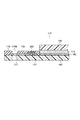
図5は、図4に示す情報表示器110のA−A線における断面図である。情報表示器110は、一対の基板(観察側基板181,背面側基板182)を備える。観察側基板181は、透明である。情報表示領域110aは、観察側基板181に形成される。観察側基板181には、観察側電極(図4、図5には不図示)が形成されている。また、背面側基板182には、背面側電極192が形成されている。一対の表示用電極(観察側電極、背面側電極)が形成された一対の基板間には、所定の間隔(ギャップ)が形成されており、観察側電極と背面側電極との間には、表示媒体層115が配置されている。   FIG. 5 is a cross-sectional view taken along line AA of the information display 110 shown in FIG. The information display 110 includes a pair of substrates (observation side substrate 181 and back side substrate 182). The observation side substrate 181 is transparent. The information display area 110a is formed on the observation side substrate 181. An observation side electrode (not shown in FIGS. 4 and 5) is formed on the observation side substrate 181. Further, a back side electrode 192 is formed on the back side substrate 182. A predetermined gap (gap) is formed between a pair of substrates on which a pair of display electrodes (observation side electrode, back side electrode) is formed, and between the observation side electrode and the back side electrode, A display medium layer 115 is disposed.

図2では、各情報表示器の向きを揃えて、すなわち、各情報表示器の表示画面を上にして重ねている様子を示しているが、2枚の情報表示器の背面側を貼り合せ、表裏の両面に表示画面を備えた情報表示器としてもよい。この場合にも貼り合わされた2枚の情報表示器において、絶縁部分として例えば設ける切欠部300の配置位置および配置個数で決まる絶縁部分と導通部分との配置パターンは異なる。   In FIG. 2, the direction of each information display device is aligned, that is, the display screen of each information display device is shown as being overlapped, but the back side of the two information display devices are bonded together, It is good also as an information indicator provided with a display screen on both sides. Also in this case, in the two information displays bonded together, the arrangement pattern of the insulating portion and the conductive portion determined by the arrangement position and the number of arrangement of the notch portions 300 provided as the insulating portion, for example, is different.

表示媒体層115は、帯電性粒子を含んだ粒子群が表示媒体として配置されている気体層(真空層を含む)または液体層であったり、コレステリック液晶層であったりする。いずれも表示メモリ性を備え、無給電状態でも表示させた情報(画像)を保持できる。実施形態では、表示媒体は、帯電特性及び光学的反射率を有する少なくとも2種類の粒子群であり、例えば、負帯電性白色粒子又は正帯電性黒色粒子とされている。これらの帯電性粒子は、基板間に印加された電圧で形成された電界によって観察側電極に(または背面側電極)に向けて気体中(真空中を含む)または液体中を移動する。実施形態では、背面側基板182は、情報表示領域110aよりも広く形成されており、情報表示器110の骨格をなす。背面側基板182には、電極117を介して、駆動回路200が配置されている。電極117及び駆動回路200は、絶縁膜118によって被覆されている。実施形態で適用可能な情報表示器110の一例については、後述する。   The display medium layer 115 may be a gas layer (including a vacuum layer) or a liquid layer in which particles including charged particles are arranged as a display medium, or a cholesteric liquid crystal layer. Both have display memory properties and can hold displayed information (images) even in a non-powered state. In the embodiment, the display medium is at least two types of particle groups having charging characteristics and optical reflectance, for example, negatively charged white particles or positively charged black particles. These chargeable particles move in gas (including vacuum) or liquid toward the observation side electrode (or back side electrode) by an electric field formed by a voltage applied between the substrates. In the embodiment, the back side substrate 182 is formed wider than the information display area 110 a and forms the skeleton of the information display device 110. A drive circuit 200 is disposed on the back side substrate 182 via the electrode 117. The electrode 117 and the drive circuit 200 are covered with an insulating film 118. An example of the information display device 110 applicable in the embodiment will be described later.

情報表示器110は、平面において、情報表示領域110aの外側に複数の駆動回路200a〜200eを備える。駆動回路200a〜200eは、ドライバICとも呼ばれるものであり、このドライバICはOUTPUT(パネルへの信号出力)を無効にする機能を備えており、後述する観察側電極と背面側電極との間に印加する電圧を制御することによって、情報表示領域110aに所望の情報を表示させる。情報表示領域110aの外側の孔部110hのいくつかの箇所には、情報表示器110のページ番号と対応させるように切欠部(絶縁部分)300が形成されている。従って、情報表示システムが備える複数の情報表示器においてこの切欠部(絶縁部分)が設けられた孔部110hの配置位置および配置個数によるパターンはそれぞれ異なる。制御装置側に備えるCPU20から複数の情報表示器がそれぞれに備える駆動回路に対して制御信号が送信される。制御信号は、後述する判定回路に送信される識別信号と、情報表示器110に表示する描画データを含む描画データ信号とを含む。   The information display device 110 includes a plurality of drive circuits 200a to 200e on the outside of the information display region 110a in a plan view. The drive circuits 200a to 200e are also called driver ICs, and this driver IC has a function of invalidating OUTPUT (signal output to the panel), and is provided between an observation side electrode and a back side electrode, which will be described later. By controlling the voltage to be applied, desired information is displayed in the information display area 110a. Cutout portions (insulating portions) 300 are formed at some positions of the hole 110 h outside the information display area 110 a so as to correspond to the page numbers of the information display 110. Therefore, in the plurality of information displays provided in the information display system, the patterns depending on the arrangement position and the number of arrangement of the holes 110h provided with the notches (insulating portions) are different. A control signal is transmitted from the CPU 20 provided on the control device side to the drive circuits provided in each of the plurality of information displays. The control signal includes an identification signal transmitted to a determination circuit described later and a drawing data signal including drawing data to be displayed on the information display 110.

本実施形態では、制御装置の複数の突出部121は、識別信号送信部123b、123d、123f、123h、123j、123lと、導通接続部124a、124c、124e、124g、124i、124kと、係合部123Xと、を有する。識別信号送信部123b、123d、123f、123h、123j、123lは、CPUからの制御信号に含まれる識別信号をすべての情報表示器110に対して送信する。各情報表示器110は、送信された識別信号について判定回路310によって、自身が表示する制御信号(描画データ信号)であるか、そうでない制御信号(描画データ信号)であるかを判定する。この判定方法については、図9等を用いて詳細に後述する。   In the present embodiment, the plurality of protrusions 121 of the control device are engaged with the identification signal transmission units 123b, 123d, 123f, 123h, 123j, and 123l, the conduction connection units 124a, 124c, 124e, 124g, 124i, and 124k. Part 123X. The identification signal transmission units 123b, 123d, 123f, 123h, 123j, and 123l transmit the identification signal included in the control signal from the CPU to all the information displays 110. Each information display 110 determines whether the transmitted identification signal is a control signal (drawing data signal) displayed by itself or a control signal (drawing data signal) that is not displayed by the determination circuit 310. This determination method will be described later in detail with reference to FIG.

導通接続部124a、124c、124e、124g、124i、124kは、情報表示器110の後述する導通接続部と電気的に接続される。係合部123Xは、情報表示器110の孔部(貫通孔)1131Xに挿入されて、複数の情報表示器110を束ねる機能を有する。なお、本実施の形態では、複数の突出部121のうち、両端の突出部121を係合部123Xとして構成しているが、係合部123Xは、別の突出部121によって構成してもよいし、1個であってもよいし、3個以上であってもよい。また、突出部121は、係合部123Xを備えていなくてもよい。   The conductive connection portions 124a, 124c, 124e, 124g, 124i, and 124k are electrically connected to a conductive connection portion, which will be described later, of the information display 110. The engaging portion 123X is inserted into the hole (through hole) 1131X of the information display device 110 and has a function of bundling a plurality of information display devices 110. In the present embodiment, among the plurality of projecting portions 121, the projecting portions 121 at both ends are configured as engaging portions 123X, but the engaging portion 123X may be configured by another projecting portion 121. It may be one, or three or more. Moreover, the protrusion part 121 does not need to be provided with the engaging part 123X.

本実施形態では、情報表示器110の複数の孔部(貫通孔)110hは、導電性の部材を備えて導通部分を構成する孔部と、導電性の部材を備えずに導通部分を構成しない孔部とを有する。導通部分を構成する孔部は、突出部121の識別信号送信部123b、123d、123f、123h、123j、123lに対応して識別信号を受信する識別信号受信部1131b、1131d、1131f、1131h、1131j、1131lと、制御装置の導通接続部124a、124c、124e、124g、124i、124kと電気的に接続される導通接続部1131a、1131c、1131e、1131g、1131i、1131kとを有する。導通部分を構成しない孔部は、制御装置の係合部123Xが挿入され、制御装置と情報表示器110とを物理的、機械的に接続するための係合孔部(貫通孔)1131Xである。   In the present embodiment, the plurality of hole portions (through holes) 110h of the information display device 110 include a conductive member and a conductive portion, and do not include a conductive member. And a hole. The holes constituting the conducting portions are identification signal receivers 1131b, 1131d, 1131f, 1131h, and 1131j that receive the identification signals corresponding to the identification signal transmitters 123b, 123d, 123f, 123h, 123j, and 123l of the protrusion 121. 1131l and conductive connection portions 1131a, 1131c, 1131e, 1131g, 1131i, and 1131k electrically connected to the conductive connection portions 124a, 124c, 124e, 124g, 124i, and 124k of the control device. The hole portion that does not constitute the conduction portion is an engagement hole portion (through hole) 1131X for physically and mechanically connecting the control device and the information display 110 by inserting the engagement portion 123X of the control device. .

係合孔部1131Xは、機械的係合にのみ用いる孔部であり、導電性の部材を備えていない孔部とすることができるが、もちろん、導電性の部材を備えた孔部とすることもできる。係合部123Xは機械的係合にのみ用いる突出部であり、導電性の部材を備えていない突出部とすることができるが、もちろん、導電性の部材を備えた突出部とすることもできる。なお、本実施の形態では、複数の孔部110hのうち係合部に対応する両端の孔部を係合孔部1131Xとして構成しているが、係合孔部1131Xは、導電性の部材を備える別の孔部よって構成してもよいし、導電性の部材を備えない孔部によって構成してもよいし、1個であってもよいし、3個以上であってもよい。また、情報表示器110は、係合孔部1131Xを備えていなくてもよい。   The engagement hole portion 1131X is a hole portion used only for mechanical engagement, and can be a hole portion not provided with a conductive member, but of course, a hole portion provided with a conductive member. You can also. The engaging portion 123X is a protruding portion used only for mechanical engagement, and can be a protruding portion that does not include a conductive member, but of course, it can also be a protruding portion that includes a conductive member. . In the present embodiment, the hole portions at both ends corresponding to the engagement portion among the plurality of hole portions 110h are configured as the engagement hole portion 1131X, but the engagement hole portion 1131X is formed of a conductive member. You may comprise by another hole part provided, may be comprised by the hole part which is not provided with an electroconductive member, may be one, and may be three or more. Further, the information display 110 may not include the engagement hole portion 1131X.

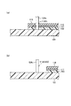
図6は、情報表示器110の識別信号受信部1131b、1131d、1131f、1131h、1131j、1131lと、識別信号受信部以外の導通部分である導通接続部1131a、1131c(不図示、絶縁部分1132(切欠部300)として図示)、1131e、1131g、1131i、1131kおよび情報表示器が備える判定回路の構成を示した部分拡大図である。図7(a)は、識別信号送信部123h及び識別信号受信部1131hを通る断面における情報表示器の部分断面図であり、図7(b)は、導通接続部124c及び絶縁部分1132(切欠部300)を通る断面における情報表示器の部分断面図である。   FIG. 6 shows identification signal receivers 1131b, 1131d, 1131f, 1131h, 1131j, and 1131l of the information display 110, and conductive connection parts 1131a and 1131c (not shown, insulating part 1132 (not shown) which are conductive parts other than the identification signal receiver. It is shown as a notch 300). FIG. 13B is a partially enlarged view showing the configuration of a determination circuit included in 1131e, 1131g, 1131i, 1131k and an information display. FIG. 7A is a partial cross-sectional view of the information display device in a cross section passing through the identification signal transmitting unit 123h and the identification signal receiving unit 1131h, and FIG. 7B is a conductive connection unit 124c and an insulating portion 1132 (notched portion). 300) is a partial cross-sectional view of the information display in a cross section passing through 300).

情報表示器110において、識別信号受信部1131b、1131d、1131f、1131h、1131j、1131l(図中、●印の部分)以外の導通接続部1131a、1131c、1131e、1131g、1131i、1131k(図中、○印の部分)において絶縁部分が形成される。ここでは、別の情報表示器においては導通部分となる1131cの部分に、切欠部300として絶縁部分1132が形成されている。識別信号受信部1131b、1131d、1131f、1131h、1131j、1131l及び導通接続部1131a、1131c、1131e、1131g、1131i、1131kは、互いに隣接配置されて判定回路を構成している。   In the information display 110, the conductive connection portions 1131a, 1131c, 1131e, 1131g, 1131i, and 1131k (in the drawing, except for the identification signal receiving portions 1131b, 1131d, 1131f, 1131h, 1131j, and 1131l (indicated by the mark ●). An insulating portion is formed in a portion marked with a circle. Here, in another information display, an insulating portion 1132 is formed as a notch portion 300 at a portion 1131c which is a conductive portion. The identification signal receiving units 1131b, 1131d, 1131f, 1131h, 1131j, 1131l and the conductive connection units 1131a, 1131c, 1131e, 1131g, 1131i, 1131k are arranged adjacent to each other to form a determination circuit.

この判定回路を構成している識別信号受信部以外の導通部分において、絶縁部分として例えば設ける切欠部300の配置位置および配置個数で決まる絶縁部分と導通部分との配置パターンは、情報表示器ごとに異なる。導電性の部材を備えた突出部121のうち導通接続部124cは、切欠部300において、情報表示器110と電気的に接続されない。すなわち、切欠部300は絶縁部分1132を構成する。   In the conductive portion other than the identification signal receiving portion constituting this determination circuit, the arrangement pattern of the insulating portion and the conductive portion determined by the arrangement position and the number of arrangement of the notch portions 300 provided as the insulating portion, for each information display Different. The conductive connection portion 124 c of the protruding portion 121 including a conductive member is not electrically connected to the information display 110 at the cutout portion 300. That is, the notch 300 constitutes an insulating portion 1132.

(3)識別信号受信部の構成
情報表示器110の判定回路を構成する導通部分は、識別信号受信部1131b、1131d、1131f、1131h、1131j、1131lと、導通接続部1131a、1131c、1131e、1131g、1131i、1131kとで構成される。導通接続部1131a、1131c、1131e、1131g、1131i、1131kには、絶縁部分1132(例えば切欠部300)が少なくとも一つ設けられる。識別信号受信部1131b、1131d、1131f、1131h、1131j、1131lは、識別信号を送信する制御装置120の識別信号送信部123b、123d、123f、123h、123j、123lと電気的に接続される。導通接続部1131a、1131c、1131e、1131g、1131i、1131kは、制御装置120の導通接続部124a、124c、124e、124g、124i、124kと電気的に接続されるが、この情報表示器110において導電部分1131cは、絶縁部分1132とされるので、制御装置120の導通接続部124cと電気的に絶縁される。
(3) Configuration of Identification Signal Receiving Unit The conductive portions constituting the determination circuit of the information display 110 are the identification signal receiving units 1131b, 1131d, 1131f, 1131h, 1131j, and 1131l, and the conductive connection units 1131a, 1131c, 1131e, and 1131g. 1131i and 1131k. At least one insulating portion 1132 (for example, the notch portion 300) is provided in the conductive connection portions 1131a, 1131c, 1131e, 1131g, 1131i, and 1131k. The identification signal receivers 1131b, 1131d, 1131f, 1131h, 1131j, and 1131l are electrically connected to the identification signal transmitters 123b, 123d, 123f, 123h, 123j, and 123l of the control device 120 that transmits the identification signal. The conductive connection portions 1131a, 1131c, 1131e, 1131g, 1131i, and 1131k are electrically connected to the conductive connection portions 124a, 124c, 124e, 124g, 124i, and 124k of the control device 120. Since the portion 1131 c is an insulating portion 1132, it is electrically insulated from the conductive connection portion 124 c of the control device 120.

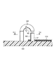
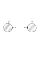
図6の絶縁部分1132は切欠部として示しているが、切り欠きではなく孔部(貫通孔)とすることもできる。絶縁部分1132が切り欠きではなく孔部(貫通孔)として形成される孔部110hにおいては導電性部材を少なくとも孔の内側に露出させない。そしてその孔径は、対応する位置にある制御装置側の導電性の部材を備えた突出部である導通接続部124cの直径よりも大きい。   Although the insulating portion 1132 in FIG. 6 is shown as a notch, it may be a hole (through hole) instead of a notch. In the hole portion 110h in which the insulating portion 1132 is formed as a hole portion (through hole) rather than a notch, the conductive member is not exposed at least inside the hole. And the hole diameter is larger than the diameter of the conduction | electrical_connection connection part 124c which is a protrusion part provided with the electroconductive member by the side of the control apparatus in a corresponding position.

絶縁部分1132を孔部(貫通孔)として形成する場合、貫通孔の孔径は、導通接続部1131a、1131b、1131d、1131e、1131f、1131g、1131h、1131i、1131j、1131k、1131lが形成された貫通孔の孔径よりも大きくする。実施形態では、絶縁部分1132は、貫通孔を円形ではなく貫通孔の面積よりも大きな面積の矩形に切り欠いた切欠部300としている。導通接続部1131cとなる孔部110hにおいて孔径を大きくして形成した孔部110hは、導通接続部124cに接触しないので電気的に絶縁される絶縁部分1132となる。   When the insulating portion 1132 is formed as a hole (through hole), the hole diameter of the through hole is a through hole in which the conductive connection portions 1131a, 1131b, 1131d, 1131e, 1131f, 1131g, 1131h, 1131i, 1131j, 1131k, 1131l are formed. It is larger than the hole diameter of the hole. In the embodiment, the insulating portion 1132 is a notch 300 in which the through hole is not circular but is cut into a rectangle having an area larger than the area of the through hole. The hole portion 110h formed by increasing the hole diameter in the hole portion 110h that becomes the conductive connection portion 1131c does not come into contact with the conductive connection portion 124c, and thus becomes an insulating portion 1132 that is electrically insulated.

なお、図6では切欠部300を設けて絶縁部分1132を形成している例を示しているが、図6において、導通接続部1131a、1131c、1131e、1131g、1131i、1131kから論理回路側に延びる配線を断線させて絶縁部分1132を形成してもよい。この場合には、絶縁部分1132とする孔部110hも他の導通接続部1131a、1131c、1131e、1131g、1131i、1131kとする孔部110hと同様に設けておくことができる。   6 shows an example in which the notch portion 300 is provided to form the insulating portion 1132. In FIG. 6, the conductive connection portions 1131a, 1131c, 1131e, 1131g, 1131i, and 1131k extend to the logic circuit side. The insulating portion 1132 may be formed by disconnecting the wiring. In this case, the hole 110h serving as the insulating portion 1132 can also be provided in the same manner as the hole 110h serving as the other conductive connection portions 1131a, 1131c, 1131e, 1131g, 1131i, and 1131k.

図8は、情報表示器110の平面視において導電性の部材を備えた孔部110h(導通接続部1131aが形成された孔部)を拡大した拡大図である。情報表示器110の背面側(ここでは背面側基板182)に形成された孔部110hは、貫通されている。図8に示すように、電極117は、露出部117aを有する。露出部117aは、孔部110hの中心に向けて突出し、露出している。露出部117aは、導電性の部材を備えた突出部(図2では121)と接触することにより、情報表示器110と制御装置120とが電気的に導通可能になる。図5に示す例では、孔部110hを情報表示器の背面側基板に設けているが、孔部110hは、情報表示器の一辺に実装されたテープキャリアパッケージ(TCP)やフレキシブル回路基板(FPC)に設けることもできる。   FIG. 8 is an enlarged view in which a hole 110h (a hole in which the conductive connection portion 1131a is formed) provided with a conductive member in the plan view of the information display 110 is enlarged. The hole 110h formed on the back side of the information display 110 (here, the back side substrate 182) is penetrated. As shown in FIG. 8, the electrode 117 has an exposed portion 117a. The exposed portion 117a protrudes toward the center of the hole portion 110h and is exposed. The exposed portion 117a comes into contact with a protruding portion (121 in FIG. 2) provided with a conductive member, so that the information display device 110 and the control device 120 can be electrically connected. In the example shown in FIG. 5, the hole 110 h is provided in the back side substrate of the information display. However, the hole 110 h may be a tape carrier package (TCP) or a flexible circuit board (FPC) mounted on one side of the information display. ).

(4)判定回路の回路構成
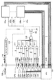
図9は、実施形態に係る情報表示器110の識別信号受信部1131b、1131d、1131f、1131h、1131j、1131lに設けられる判定回路の回路構成を説明する回路図である。図9には、識別信号を含む制御信号を送信するCPU20及び、切欠部300として示した絶縁部分1132、制御装置120側および情報表示器110側の導通部分の近傍の一部が示されている。図10は、実施形態に係る情報表示器110に配置される駆動回路200a〜200eと、駆動回路200a〜200eに接続される接続線を説明する図である。
(4) Circuit Configuration of Determination Circuit FIG. 9 is a circuit diagram illustrating the circuit configuration of the determination circuit provided in the identification signal receiving units 1131b, 1131d, 1131f, 1131h, 1131j, and 1131l of the information display device 110 according to the embodiment. is there. FIG. 9 shows a part of the CPU 20 that transmits a control signal including an identification signal, the insulating portion 1132 shown as the notch 300, and the vicinity of the conductive portion on the control device 120 side and the information display 110 side. . FIG. 10 is a diagram illustrating drive circuits 200a to 200e arranged in the information display device 110 according to the embodiment and connection lines connected to the drive circuits 200a to 200e.

識別信号受信部1131b、1131d、1131f、1131h、1131j、1131lは、制御装置120の導電性の部材を備えた突出部121のうち識別信号送信部123b、123d、123f、123h、123j、123lと電気的に接続される。識別信号受信部以外の導通接続部1131a、1131c(図9では切欠部300として図示)、1131e、1131g、1131i、1131kは、制御装置120の導通接続部124a、124c、124e、124g、124i、124kと電気的に接続される。この導通接続部1131a、、1131c、1131e、1131g、1131h、1131kの少なくとも一つに、制御装置120側と電気的に接続されない絶縁部分1132(例えば切欠部300)を設ける。   The identification signal receivers 1131b, 1131d, 1131f, 1131h, 1131j, and 1131l are electrically connected to the identification signal transmitters 123b, 123d, 123f, 123h, 123j, and 123l among the protrusions 121 that include the conductive member of the control device 120. Connected. Conductive connection portions 1131a, 1131c (illustrated as notch portions 300 in FIG. 9) other than the identification signal receiving portion, 1131e, 1131g, 1131i, 1131k are conductive connection portions 124a, 124c, 124e, 124g, 124i, 124k of the control device 120. And electrically connected. At least one of the conductive connection portions 1131a, 1131c, 1131e, 1131g, 1131h, and 1131k is provided with an insulating portion 1132 (for example, the notch portion 300) that is not electrically connected to the control device 120 side.

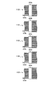
図9に示す情報表示器110では、他の情報表示器において導通接続部1131cとなる部分に絶縁部分1132を切欠部300として形成することによって、1個の絶縁部分と5個の導通接続部との配置パターンを構成して、当該情報表示器の識別情報としている。図6に示すような識別信号受信部以外の導通接続部を6個、判定回路に設けた構成の情報表示器110においては、1個から6個まで絶縁部分を設けることができ、〔26−1〕通りの配置パターンを得ることができる。 In the information display 110 shown in FIG. 9, one insulating portion and five conductive connection portions are formed by forming an insulating portion 1132 as the notch portion 300 in a portion that becomes the conductive connection portion 1131 c in another information display device. The arrangement pattern is configured as identification information of the information display. In the information display device 110 having a configuration in which six conductive connection portions other than the identification signal receiving portion as shown in FIG. 6 are provided in the determination circuit, one to six insulating portions can be provided, and [2 6 -1] It is possible to obtain various arrangement patterns.

なお、絶縁部分は、1つの情報表示器110において、1個設けてもよいし、複数個設けてもよい。また、情報表示システムが備える複数の情報表示器のうち1つの情報表示器は、絶縁部分が設けられていなくもよい。すなわち、複数の情報表示器において、絶縁部分の配置パターンが互いに異なるように構成されていればよい。   One insulating part may be provided in one information display 110, or a plurality of insulating parts may be provided. In addition, one information display device among the plurality of information display devices provided in the information display system may not be provided with an insulating portion. In other words, the plurality of information displays may be configured such that the arrangement patterns of the insulating portions are different from each other.

なお、識別信号受信部1131b、1131d、1131f、1131h、1131j、1131l、導通接続部1131a、1131e、1131g、1131h、1131k、及び絶縁部分1132は、例えば図9に示すように形成されて、XNOR回路311、NAND回路312を論理回路として備えた判定回路310を構成して、識別信号受信部1131b、1131d、1131f、1131h、1131j、1131lを介して受信した識別信号と、当該情報表示器における絶縁部分(導通接続部に形成される絶縁部分)と導通部分(導通接続部に形成される導通部分)との配置パターンで決められた識別情報とを比較して一致するか一致しないかを判定し、判定結果に応じて当該情報表示器が備える駆動回路200a〜200eのアウトプットイネーブル(OUTPUT−ENABLE)を有効にしたり無効にしたりできるように駆動回路200a〜200eと電気的に接続されるように構成されている。   The identification signal receiving units 1131b, 1131d, 1131f, 1131h, 1131j, 1131l, the conductive connection units 1131a, 1131e, 1131g, 1131h, 1131k, and the insulating portion 1132 are formed as shown in FIG. 311, a determination circuit 310 including a NAND circuit 312 as a logic circuit is configured, and the identification signal received via the identification signal receivers 1131b, 1131d, 1131f, 1131h, 1131j, and 1131l, and an insulating portion in the information display Comparing the identification information determined by the arrangement pattern of the (insulating part formed in the conductive connection part) and the arrangement pattern of the conductive part (conductive part formed in the conductive connection part) to determine whether they match or not, Depending on the determination result, the drive circuits 200a to 20 provided in the information display device It is configured to be electrically connected to a driving circuit 200a~200e to allow or disable enable e output enable (OUTPUT-ENABLE).

判定回路310の出力線は分岐されており、駆動回路200a〜200eの各々に接続されている。ここでは、駆動回路200a〜200eのアウトプットイネーブル用ライン320a〜320eに接続している。   The output line of the determination circuit 310 is branched and connected to each of the drive circuits 200a to 200e. Here, they are connected to the output enable lines 320a to 320e of the drive circuits 200a to 200e.

図9に示す例とは異なる回路配線にして、駆動回路200a〜200eのチップセレクト用ライン320a〜320eに接続するような構成にすることもでき、判定回路を構成する回路配線は、図9に示す例に限定されるものではない。   The circuit wiring different from the example shown in FIG. 9 may be connected to the chip select lines 320a to 320e of the drive circuits 200a to 200e. The circuit wiring constituting the determination circuit is shown in FIG. It is not limited to the example shown.

判定回路には、当該情報表示器を特定するための識別情報が必要である。上述の図9に示した実施形態では、判定回路内に形成した絶縁部分1132(切欠部300)の個数と位置とで決められる配置パターンが上記識別情報として形成されているが、識別情報はこれに限られず、当該情報表示器を特定する情報、例えばページ番号を記憶させたICチップ(メモリ)を設けて、制御装置から描画データとともに送信された識別信号と、メモリに記憶させてあるページ番号情報とを比較して、一致か不一致かを判定するような構成にすることもできる。   The determination circuit needs identification information for specifying the information display. In the embodiment shown in FIG. 9 described above, an arrangement pattern determined by the number and positions of insulating portions 1132 (notches 300) formed in the determination circuit is formed as the identification information. The identification number transmitted with the drawing data from the control device, and the page number stored in the memory, provided with an IC chip (memory) that stores information specifying the information display, for example, the page number, is not limited thereto It is also possible to make a configuration that compares information with each other to determine whether it matches or does not match.

図9に示したように、絶縁部分1132(例えば、切欠部300)を備えた情報表示器の方が、ICチップメモリを備えた情報表示器よりも回路構成が簡単であるとともに、高価なICチップを要しないことで安価にできるという利点がある。   As shown in FIG. 9, the information display device including the insulating portion 1132 (for example, the notch 300) has a simpler circuit configuration than the information display device including the IC chip memory, and the expensive IC. There is an advantage that it can be made inexpensive by not requiring a chip.

(5)情報表示器に情報を表示する処理
次いで、図11に基づいて、判定回路の具体的な判定態様、及び制御装置120が複数の情報表示器110に情報を表示する処理について説明する。図11は、制御装置120が複数の情報表示器110に情報を表示する処理を説明するフローチャートである。以下に示す具体例では、1つの制御装置に64枚の情報表示器110が綴じられており、2頁目にあたる#2情報表示器のデータを表示する場合を説明する。よって、制御装置のCPUから2ページ目を識別するための識別信号を含んだ制御信号を送信し、2ページ目に描画データ信号に基づく画像を表示させる。
(5) Process for Displaying Information on Information Display Next, a specific determination mode of the determination circuit and a process for the control device 120 to display information on the plurality of information displays 110 will be described based on FIG. FIG. 11 is a flowchart illustrating a process in which the control device 120 displays information on the plurality of information displays 110. In the specific example shown below, a case will be described in which 64 information displays 110 are bound in one control device and data of the # 2 information display corresponding to the second page is displayed. Therefore, a control signal including an identification signal for identifying the second page is transmitted from the CPU of the control device, and an image based on the drawing data signal is displayed on the second page.

ステップ1において、制御装置120は、制御信号を情報表示器110に対して送信する。具体的には、描画データ信号送信部122を介して、情報表示領域110aに所望の情報を表示させるための描画データ信号を情報表示器110に対して送信し、識別信号送信部123b、123d、123f、123h、123j、123lを介して、判定回路において情報表示器110を識別するための識別信号を情報表示器110に対して送信する。   In step 1, the control device 120 transmits a control signal to the information display 110. Specifically, a drawing data signal for displaying desired information in the information display area 110a is transmitted to the information display 110 via the drawing data signal transmission unit 122, and the identification signal transmission units 123b, 123d, An identification signal for identifying the information display 110 in the determination circuit is transmitted to the information display 110 through 123f, 123h, 123j, and 123l.

描画データ信号送信部122からの描画データ信号は、情報表示器110の描画データ信号受信部1120によって受信し、駆動回路200a〜200eに入力される。なお、識別信号および描画データ信号は、全ての情報表示器110に対して送信される。   The drawing data signal from the drawing data signal transmission unit 122 is received by the drawing data signal reception unit 1120 of the information display 110 and input to the drive circuits 200a to 200e. The identification signal and the drawing data signal are transmitted to all the information displays 110.

ステップ21において、#2情報表示器は、識別信号受信部1131b、1131d、1131f、1131h、1131j、1131lで受信した識別信号と、絶縁部分1132(切欠部300)と導通接続部1131a、1131e、1131g、1131h、1131kとの配置パターンとで決まる識別情報と、を比較して一致しているか一致していないかを判定する。   In step 21, the # 2 information display unit receives the identification signals received by the identification signal receiving units 1131b, 1131d, 1131f, 1131h, 1131j, and 1131l, the insulating portion 1132 (the notch portion 300), and the conductive connection portions 1131a, 1131e, and 1131g. The identification information determined by the arrangement patterns 1131h and 1131k is compared to determine whether they match or do not match.

具体的には、制御装置120の識別信号送信部123b、123d、123f、123h、123j、123lから情報表示器110側の判定回路に、2ページ目に表示すべき識別信号(例えば、「010000」)が64枚全ての情報表示器110に対して送信される。#2情報表示器は、識別信号受信部1131b、1131f、1131h、1131j、1131lの出力が「0」となる。一方、識別信号受信部1131dの出力が「1」となる。また、導通接続部1131a、1131e、1131g、1131i、1131kの出力は、導通接続部124a、124e、124g、124i、124kを介して接地されて、「0」となる。一方、切欠部300が形成された部分は、接地されないため「1」が出力される。よって、#2情報表示器110では、判定回路310のXNOR回路311の出力側の真理値は、「111111」となる。全てのXNOR回路311の出力が「1」となり、NAND回路312の出力は「0」となる。すなわち、#2情報表示器においては、#2情報表示器の識別情報と受信した識別信号とが一致する(ステップ21:YES)。   Specifically, the identification signal to be displayed on the second page from the identification signal transmission units 123b, 123d, 123f, 123h, 123j, 123l of the control device 120 to the determination circuit on the information display device 110 side (for example, “010000”). ) Is transmitted to all 64 information displays 110. In the # 2 information display, the outputs of the identification signal receivers 1131b, 1131f, 1131h, 1131j, and 1131l are “0”. On the other hand, the output of the identification signal receiving unit 1131d is “1”. Further, the outputs of the conductive connection portions 1131a, 1131e, 1311, g, 1311, i, and 1311k are grounded via the conductive connection portions 124a, 124e, 124g, 124i, and 124k, and become “0”. On the other hand, since the portion where the notch 300 is formed is not grounded, “1” is output. Therefore, in the # 2 information display 110, the truth value on the output side of the XNOR circuit 311 of the determination circuit 310 is “111111”. The outputs of all the XNOR circuits 311 are “1”, and the outputs of the NAND circuits 312 are “0”. That is, in the # 2 information display device, the identification information of the # 2 information display device matches the received identification signal (step 21: YES).

よって、スイッチ350がオフ(OFF)となって(ステップ31)、駆動回路200a〜200eのアウトプットイネーブル(OUTPUT−ENABLE)が有効となり(ステップ41)、CPUからの出力信号を受信した際に、駆動回路200a〜200eから情報表示器の情報表示領域110aへ描画データが出力される(ステップ51)。よって、#2情報表示器の書き換えが実行される(ステップ61)。   Therefore, when the switch 350 is turned off (OFF) (step 31), the output enable (OUTPUT-ENABLE) of the drive circuits 200a to 200e is enabled (step 41), and the output signal from the CPU is received. Drawing data is output from the drive circuits 200a to 200e to the information display area 110a of the information display (step 51). Therefore, the # 2 information display is rewritten (step 61).

一方、他のページ、例えば、1ページ目にあたる#1情報表示器は、導通接続部1131aに対応する部分に切り欠きが形成されている。ステップ1において、制御装置120が、#1情報表示器に対して制御信号(2ページ目に表示する描画データと2ページ目を識別するための識別信号)を送信すると、#1情報表示器は、識別信号受信部1131b、1131d、1131f、1131h、1131j、1131lで受信した識別信号と、絶縁部分1132(切欠部300)と導通接続部1131a、1131e、1131g、1131h、1131kとの配置パターンとで決まる識別情報と、を比較して一致しているか一致していないかを判定する。   On the other hand, in the # 1 information display corresponding to the other page, for example, the first page, a notch is formed in a portion corresponding to the conductive connection portion 1131a. In Step 1, when the control device 120 transmits a control signal (drawing data displayed on the second page and an identification signal for identifying the second page) to the # 1 information display, the # 1 information display The identification signals received by the identification signal receiving units 1131b, 1131d, 1131f, 1131h, 1131j, and 1131l, and the arrangement pattern of the insulating portions 1132 (notched portions 300) and the conductive connection portions 1131a, 1131e, 1131g, 1131h, and 1131k The determined identification information is compared to determine whether or not they match.

具体的には、制御装置120の識別信号送信部123b、123d、123f、123h、123j、123lから#1情報表示器110側の判定回路に、2ページ目に表示すべき描画データであることを識別するための識別信号(例えば、「010000」)が送信される。   Specifically, it is the drawing data to be displayed on the second page from the identification signal transmission units 123b, 123d, 123f, 123h, 123j, 123l of the control device 120 to the determination circuit on the # 1 information display 110 side. An identification signal (for example, “010000”) for identification is transmitted.

識別信号受信部1131b、1131f、1131h、1131j、1131lの出力は、「0」となる。一方、識別信号受信部1131dの出力は、「1」となる。また、導通接続部1131c、1131e、1131g、1131i、1131kの出力は、導通接続部124c、124e、124g、124i、124kを介して接地されて、「0」となる。一方、切欠部300が形成された部分は、接地されないため「1」が出力される。よって、#1情報表示器110では、判定回路310のXNOR回路311の出力側の真理値は、「001111」となる。全てのXNOR回路311の出力が「1」とならないため、NAND回路312の出力は「1」となる。すなわち、#1情報表示器においては、#1情報表示器の識別情報と受信した識別信号とが一致しない(ステップ21:NO)。   The outputs of the identification signal receiving units 1131b, 1131f, 1131h, 1131j, and 1131l are “0”. On the other hand, the output of the identification signal receiving unit 1131d is “1”. Further, the outputs of the conductive connection portions 1131c, 1131e, 1311, g, 1311, i, and 1311k are grounded via the conductive connection portions 124c, 124e, 124g, 124i, and 124k, and become “0”. On the other hand, since the portion where the notch 300 is formed is not grounded, “1” is output. Therefore, in the # 1 information display 110, the truth value on the output side of the XNOR circuit 311 of the determination circuit 310 is “001111”. Since the outputs of all the XNOR circuits 311 are not “1”, the output of the NAND circuit 312 is “1”. That is, in the # 1 information display, the identification information of the # 1 information display and the received identification signal do not match (step 21: NO).

よって、スイッチ350がオン(ON)となって(ステップ32)、駆動回路200a〜200eのアウトプットイネーブル(OUTPUT−ENABLE)が無効となり(ステップ42)、CPUからの出力信号を受信しても、駆動回路200a〜200eから情報表示器の情報表示領域110aへ描画データが出力されない(ステップ52)。よって、#1情報表示器(#2情報表示器以外の他の情報表示器も同様)の書き換えが実行されない(ステップ62)。   Accordingly, the switch 350 is turned on (step 32), the output enable (OUTPUT-ENABLE) of the drive circuits 200a to 200e is invalidated (step 42), and the output signal from the CPU is received. Drawing data is not output from the drive circuits 200a to 200e to the information display area 110a of the information display (step 52). Therefore, rewriting of the # 1 information display (similar to other information displays other than the # 2 information display) is not executed (step 62).

なお、ここでは、1ページ目にあたる#1情報表示器を例に挙げて説明しているが、3ページ目にあたる#3情報表示器、4ページ目にあたる#4情報表示器、5ページ目にあたる#5情報表示器のほか64ページ目にあたる#64情報表示器までの他の情報表示器については、#1情報表示器110同様に、入力された識別信号と切欠部300の配置パターンが一致せず、書き換えが実行されない。   In this example, the # 1 information display corresponding to the first page is described as an example. However, the # 3 information display corresponding to the third page, the # 4 information display corresponding to the fourth page, and the # 5 information corresponding to the fifth page are described. For other information displays up to # 64 information display corresponding to the 64th page in addition to the 5 information display, the input identification signal and the arrangement pattern of the notch 300 do not match, as in the # 1 information display 110. , Rewriting is not performed.

このように、情報表示システム100では、識別信号受信部1131b、1131d、1131f、1131h、1131j、1131lで受信した識別信号と、絶縁部分1132(切欠部300)と導通接続部1131a、1131e、1131g、1131h、1131kとの配置パターンで決まる識別情報とを比較して一致しているか一致していないかを判定する判定回路310を備えており、識別信号と識別情報とが一致した情報表示器110の情報表示領域110aに、駆動回路200a〜200eから描画データが出力される。これにより、制御装置120から送信された識別信号に一致した情報表示器110にだけ、この識別信号を含んだ制御信号に基づいた所定の描画データに基づいた情報(表示させたい情報)が表示される。   As described above, in the information display system 100, the identification signal received by the identification signal receivers 1131b, 1131d, 1131f, 1131h, 1131j, and 1131l, the insulating portion 1132 (the notch portion 300), and the conductive connection portions 1131a, 1131e, and 1131g, The information display device 110 includes a determination circuit 310 that compares the identification information determined by the arrangement patterns 1131h and 1131k to determine whether the identification information matches or does not match. Drawing data is output from the drive circuits 200a to 200e to the information display area 110a. As a result, information (information to be displayed) based on predetermined drawing data based on the control signal including the identification signal is displayed only on the information display 110 that matches the identification signal transmitted from the control device 120. The

また、上記本発明の実施形態で示した判定回路の構成は一例である。上記実施形態では絶縁部分(切欠部)と、CPUの各端子からの入力をXNOR論理回路で比較しているが、例えば、CPU端子からの入力を一度シフトレジスタで受ける方法等も考えられる。このように、絶縁部分(切欠部)の配置パターンとして与えられる情報と、制御装置から送信される識別信号による情報を比較して、一致しているか一致していないかを検出して判定する回路は、本発明の実施形態に記載した論理回路(XNOR、NAND)に限定されるものではなく、他の論理回路やメモリ回路など一般的に用いられる電子回路とすることもできる。絶縁部分(切欠部)の配置パターンと、電子回路とを組み合せて判定回路を構成した情報表示器を用いて本発明の情報表示システムを構成している点に特徴がある。   The configuration of the determination circuit shown in the embodiment of the present invention is an example. In the above embodiment, the XNOR logic circuit compares the insulation portion (notch portion) and the input from each terminal of the CPU, but for example, a method of receiving the input from the CPU terminal once by the shift register is also conceivable. As described above, the information given as the arrangement pattern of the insulating portion (notch portion) and the information by the identification signal transmitted from the control device are compared, and a circuit for detecting whether or not they match is determined. Is not limited to the logic circuit (XNOR, NAND) described in the embodiment of the present invention, and may be a commonly used electronic circuit such as another logic circuit or a memory circuit. The present invention is characterized in that the information display system of the present invention is configured by using an information display in which a determination circuit is configured by combining an arrangement pattern of insulating portions (notches) and an electronic circuit.

(6)作用・効果
実施形態として示す情報表示システム100では、制御装置120に形成される複数の突出部121は、制御装置側連結機構を構成している。また、突出部121のうち導電性の部材を備えた突出部121のいくつかは、駆動回路200a〜200eを制御する制御信号を送信する制御信号送信部を構成している。制御信号送信部のいくつかは、制御信号に含まれる識別信号(情報表示器110を識別するために送信する信号)を送信する識別信号送信部123を構成し、他の制御信号送信部のいくつかは、描画データを含む描画データ信号を送信する描画データ信号送信部122を構成している。突出部121のいくつかは、電気的接続を行わずに、単に機械的接続を行うために用いることができる。この突出部は、導電性の部材を備えていなくてもよい。
(6) Action / Effect In the information display system 100 shown as the embodiment, the plurality of projecting portions 121 formed in the control device 120 constitutes a control device side connection mechanism. In addition, some of the protrusions 121 including conductive members among the protrusions 121 constitute a control signal transmission unit that transmits a control signal for controlling the drive circuits 200a to 200e. Some of the control signal transmission units constitute an identification signal transmission unit 123 that transmits an identification signal included in the control signal (a signal transmitted to identify the information display 110), and some of the other control signal transmission units. This constitutes a drawing data signal transmission unit 122 that transmits a drawing data signal including drawing data. Some of the protrusions 121 can be used for merely making a mechanical connection without making an electrical connection. This protrusion does not need to be provided with a conductive member.

情報表示器110に形成される判定回路310を構成し、電気的接続に供される導電性の部材を備えた孔部(貫通孔)110hは、識別信号送信部と接続される識別信号受信部と、導通接続部とで構成され、ている。識別信号受信部と、導通接続部とはペアとなって配置され、絶縁部分1132(例えば切欠部300)は、この導通接続部において形成される。この導通接続部において設ける絶縁部分1132は、1個でも複数個でもよく、配置個数と配置位置との組み合わせによって複数の配置パターンが形成される。識別信号受信部113となる導通部分(導通接続部)と、それ以外の導通部分(導通接続部)とのペアがN個ある判定回路では、〔2N(2のN乗)−1〕個の配置パターンが形成できる。図9に一例として導通接続部において形成される導通接続部において形成される絶縁部分が1個の例を示したが、絶縁部分を複数(図9のように、例えば6個のXNOR回路を備える判定回路構成では6個まで)形成することができ、図9のように、導通接続部において形成される絶縁部分を少なくとも備え、導通部分と絶縁部分の配置パターンが異なる63(26−1)個の情報表示器と、絶縁部分(切欠部)がない情報表示器を1個加えた64個(26)個、すなわち、N個のXNOR回路を備える情報表示器においては、2N〔(2のN乗)〕個の情報表示器を備えた情報表示システムとすることができる。 A hole (through hole) 110h that constitutes the determination circuit 310 formed in the information display 110 and includes a conductive member used for electrical connection is an identification signal receiver connected to the identification signal transmitter And a conductive connection portion. The identification signal receiving portion and the conductive connection portion are arranged in pairs, and the insulating portion 1132 (for example, the notch portion 300) is formed in this conductive connection portion. One or a plurality of insulating portions 1132 provided in the conductive connection portion may be provided, and a plurality of arrangement patterns are formed by a combination of the arrangement number and the arrangement position. In a determination circuit having N pairs of conductive portions (conductive connection portions) serving as the identification signal receiving unit 113 and other conductive portions (conductive connection portions), [2 N (2 to the Nth power) −1] pieces. This arrangement pattern can be formed. FIG. 9 shows an example in which one insulating portion is formed in the conductive connecting portion formed in the conductive connecting portion. However, a plurality of insulating portions (for example, six XNOR circuits are provided as shown in FIG. 9). (In the determination circuit configuration, up to six) can be formed, and as shown in FIG. 9, at least an insulating portion formed in the conductive connection portion is provided, and the arrangement pattern of the conductive portion and the insulating portion is different 63 (2 6 −1) In an information display having 64 (2 6 ) information displays including one information display and one information display having no insulating portion (notch), that is, an information display including N XNOR circuits, 2 N [( 2 to the Nth power)]] information display system.

情報表示システム100では、識別信号受信部1131b、1131d、1131f、1131h、1131j、1131lで受信した識別信号と、絶縁部分1132(切欠部300)と導通接続部1131a、1131e、1131g、1131h、1131kとの配置パターンによって決まる識別情報と、を比較して一致しているか一致していないかを判定し、この識別信号とこの識別情報とが一致した情報表示器110に対してだけ駆動回路200a〜200eのアウトプットイネーブルが有効になり、制御信号(描画データ信号)に基づく出力が可能となる。そして、この識別信号とこの識別情報とが一致した情報表示器にだけ、この識別信号を含んだ制御信号(描画データ信号)に基づいた所定の情報(画像)を表示させることができる。   In the information display system 100, the identification signal received by the identification signal receivers 1131b, 1131d, 1131f, 1131h, 1131j, and 1131l, the insulating portion 1132 (the notch portion 300), the conductive connection portions 1131a, 1131e, 1131g, 1131h, and 1131k The identification information determined by the arrangement pattern is compared to determine whether or not they match, and the drive circuits 200a to 200e are only applied to the information display 110 where the identification signal and the identification information match. The output enable is enabled, and output based on the control signal (drawing data signal) becomes possible. And only the information display device in which this identification signal and this identification information correspond can display predetermined information (image) based on the control signal (drawing data signal) including this identification signal.

従って、制御装置120から送信された識別信号と一致した情報表示器110に所定の情報(画像)が表示される。また、情報表示システム100は、「ページ」を構成する複数の情報表示器110が見開き状態か否かによらず、すなわち、冊子状の情報表示システム100では、冊子を閉じたままで、所定の情報表示器110に対して、所定の情報(画像)を表示させることができる。   Accordingly, predetermined information (image) is displayed on the information display 110 that matches the identification signal transmitted from the control device 120. In addition, the information display system 100 does not depend on whether or not the plurality of information displays 110 constituting the “page” are in a spread state, that is, the booklet-shaped information display system 100 keeps the booklet closed and the predetermined information Predetermined information (image) can be displayed on the display device 110.

本実施形態に係る情報表示システム100では、制御装置120は、連結された全ての情報表示器110の判定回路に識別信号を送信し、この識別信号と、情報表示器の番号を識別するための識別情報とが一致した情報表示器110が備える駆動回路200a〜200eのみアウトプットイネーブルが有効になる。この情報表示器の番号を識別するための識別情報は、識別信号受信部以外の導通部分において、絶縁部分(切欠部)の配置位置および絶縁部分(切欠部)の配置個数と、他の導通部分との組み合わせで決まる配置パターンとして与えられ、判定回路を構成する論理回路を使って、識別信号との一致または不一致を判定し、一致した場合にスイッチ350をオフ(OFF)にして、制御装置120からの制御信号に対して、駆動回路200a〜200eのアウトプットイネーブルが有効になるように構成されている。   In the information display system 100 according to the present embodiment, the control device 120 transmits an identification signal to the determination circuits of all the linked information displays 110, and identifies the identification signal and the number of the information display. The output enable is valid only for the drive circuits 200a to 200e included in the information display 110 that matches the identification information. The identification information for identifying the number of the information display includes the arrangement position of the insulating part (notch part), the number of arrangements of the insulating part (notch part), and other conductive parts in the conductive part other than the identification signal receiving part. Is determined as a placement pattern determined by the combination of the control signal 120 and the logic circuit that constitutes the determination circuit is used to determine whether the identification signal matches or does not match, and when it matches, the switch 350 is turned off. The output enable of the drive circuits 200a to 200e is configured to be valid with respect to the control signal from.

従って、制御装置120において、複数の情報表示器110との電気的な接続部を共通化することができる。これにより、制御装置120の突出部121に複数の情報表示器110に形成された孔部110hを挿通することによって情報表示器110を冊子状にすることができる。   Therefore, in the control apparatus 120, the electrical connection part with the some information indicator 110 can be shared. Thereby, the information indicator 110 can be made into a booklet shape by inserting the holes 110 h formed in the plurality of information indicators 110 into the protruding portion 121 of the control device 120.

(7)連結機構の変形例
(7−1)変形例1
実施形態では、制御装置側連結機構は、突出部121であり、情報表示器側連結機構は、孔部110hであると説明した。制御装置側連結機構と情報表示器側連結機構との形態は変更可能である。
(7) Modification of coupling mechanism (7-1) Modification 1
In the embodiment, it has been described that the control device side coupling mechanism is the protrusion 121 and the information display side coupling mechanism is the hole 110h. The forms of the control device side coupling mechanism and the information display side coupling mechanism can be changed.

図12,13は、制御装置側連結機構の変形例を説明する図である。図12に示すように、留め具130が設けられる替わりに、外装体Cに湾曲部材140が取り付けられている。湾曲部材140の一方の端部140aは、外装体Cに取り付けられている。また、湾曲部材140の他方の端部140bは、突出部121の固定されていない端部121fに当接されている。すなわち、湾曲部材140と突出部121とによって閉じられた環状構造が形成される。   12 and 13 are diagrams illustrating a modification of the control device side coupling mechanism. As shown in FIG. 12, the bending member 140 is attached to the exterior body C instead of providing the fastener 130. One end portion 140 a of the bending member 140 is attached to the exterior body C. Further, the other end portion 140 b of the bending member 140 is in contact with an unfixed end portion 121 f of the protruding portion 121. That is, a closed annular structure is formed by the bending member 140 and the protruding portion 121.

湾曲部材140は、端部140bと突出部121の端部121fとが離間する方向に可動自在に構成されており、突出部121に挿通された情報表示器110は、リング(湾曲部材140と突出部121とによって閉じられた環状構造)から取り外すことができる。   The bending member 140 is configured to be movable in a direction in which the end portion 140b and the end portion 121f of the projecting portion 121 are separated from each other, and the information display device 110 inserted through the projecting portion 121 includes a ring (projecting from the bending member 140 and the projecting portion 121). The ring structure closed by the part 121).

湾曲部材140は、導電性の材料で形成することができる。これにより、情報表示器110を、図13における右側から左側に移動させた状態で、左側に位置する(すなわち、ユーザが見ていない情報表示器110に情報を表示させる処理を行うことができる。   The bending member 140 can be formed of a conductive material. Accordingly, it is possible to perform a process of displaying information on the information display unit 110 that is positioned on the left side (that is, the information display unit 110 that is not viewed by the user) while the information display unit 110 is moved from the right side to the left side in FIG.

(7−2)変形例2
図14は、制御装置側連結機構の別の変形例を説明する図である。図14に示すように、湾曲部材140の一方の端部140aは、回動機構150を介して外装体Cに取り付けられている。湾曲部材140は、回動機構150によって、図14の矢印方向に回動することにより、端部140bと端部121fとが離間する。
(7-2) Modification 2
FIG. 14 is a diagram illustrating another modification of the control device side coupling mechanism. As shown in FIG. 14, one end portion 140 a of the bending member 140 is attached to the exterior body C via the rotation mechanism 150. The bending member 140 is rotated in the direction of the arrow in FIG. 14 by the rotation mechanism 150, whereby the end portion 140b and the end portion 121f are separated from each other.

(8)連結機構の導通構造の変形例
情報表示システム100では、突出部121(或いは変形例1,2として示した湾曲部材140)の一部分に電気を導通する構造が形成されていてもよい。図15は、連結機構の電気を導通するための構造の変形例を説明する図である。図16は、図15に示すD−D線における断面図である。
(8) Modification Example of Conduction Structure of Connection Mechanism In the information display system 100, a structure that conducts electricity may be formed in a part of the protruding portion 121 (or the bending member 140 shown as Modification Examples 1 and 2). FIG. 15 is a diagram for explaining a modification of the structure for conducting electricity of the coupling mechanism. 16 is a cross-sectional view taken along the line DD shown in FIG.

図15には、変形例1として示した湾曲部材140と類似の形状を有する湾曲部材160が示されている。湾曲部材160は、絶縁性の材料で形成されており、絶縁性の材料の一部に導電性の材料161が配置されている。また、この変形例では、突出部121も絶縁性の材料で形成されており、突出部121の一部に導電性の材料162が配置されている。   FIG. 15 shows a bending member 160 having a shape similar to that of the bending member 140 shown as the first modification. The bending member 160 is formed of an insulating material, and a conductive material 161 is disposed in part of the insulating material. In this modification, the projecting portion 121 is also formed of an insulating material, and a conductive material 162 is disposed on a part of the projecting portion 121.

湾曲部材160及び突出部121において、導電性の材料161,162は、湾曲部材160と突出部121とによって形成される環状構造の内側の一部に配置される。   In the bending member 160 and the protruding portion 121, the conductive materials 161 and 162 are disposed on a part of the inside of the annular structure formed by the bending member 160 and the protruding portion 121.

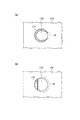
図17(a)、(b)は、図1〜図3、図12〜図15に示す連結機構における情報表示器の孔部110hの構造として図8に示した孔部の変形例である孔部170を説明する平面図である。孔部170には、孔部170の中心に向けて電極の一部が突出している。孔部170の中心に向けて突出した電極(露出電極171という)は、制御装置側の突出部に配置された導電性の材料(図16で示される例では、161,162)に対応する位置に形成されている。   17 (a) and 17 (b) are holes which are modifications of the hole shown in FIG. 8 as the structure of the hole 110h of the information display device in the coupling mechanism shown in FIGS. 1 to 3 and 12 to 15. It is a top view explaining the part 170. FIG. A part of the electrode protrudes from the hole 170 toward the center of the hole 170. The electrode projecting toward the center of the hole 170 (referred to as the exposed electrode 171) corresponds to a conductive material (161, 162 in the example shown in FIG. 16) disposed in the projecting portion on the control device side. Is formed.

図17(a)、図17(b)に示す点線で囲まれた領域Rは、電極が露出していない部分を示している。露出電極171は、図21に示す絶縁性の突出部121及び絶縁性の湾曲部材160に配置された導電性の材料161,162に対応する位置に形成されている。   A region R surrounded by a dotted line shown in FIGS. 17A and 17B indicates a portion where the electrode is not exposed. The exposed electrode 171 is formed at a position corresponding to the conductive materials 161 and 162 disposed on the insulating protrusion 121 and the insulating bending member 160 shown in FIG.

以上説明したように連結機構における制御装置側の突出部121の主たる部分を絶縁性とし一部を導電性にした導通構造を構成することにより、情報表示器110に情報を表示する処理を実行している時などに、ユーザが隣接する突出部121(或いは変形例1,2として示した湾曲部材140)同士を同時に触れてしまったとしても、ショートを防止でき、情報を表示する処理を確実に実行することができる。   As described above, a process of displaying information on the information display 110 is performed by configuring a conductive structure in which the main part of the protrusion 121 on the control device side in the coupling mechanism is insulative and partly conductive. Even if the user touches adjacent protrusions 121 (or the bending members 140 shown as the first and second modifications 1 and 2) at the same time, the short circuit can be prevented and the process of displaying information is ensured. Can be executed.

(9)情報表示器の概略構成
図18は、本実施形態に係る情報表示システム100及びこれに適用可能な情報表示器110の構成概要を説明する概略斜視図である。
(9) Schematic Configuration of Information Display FIG. 18 is a schematic perspective view for explaining the configuration outline of the information display system 100 according to the present embodiment and the information display 110 applicable thereto.

図18に示すように、情報表示器110は、一対の電極(観察側電極191,背面側電極192)と、一対の基板(観察側基板181,背面側基板182)とを備える。一対の基板間には、ギャップ確保用隔壁119a及び粒子偏在抑制用隔壁119b(図18においては、いずれも不図示。図20においては、ギャップ確保用隔壁と粒子偏在抑制用隔壁とを兼用する隔壁としてギャップ確保用隔壁を示している)とが設けられる。   As shown in FIG. 18, the information display 110 includes a pair of electrodes (observation side electrode 191, back side electrode 192) and a pair of substrates (observation side substrate 181, back side substrate 182). Between the pair of substrates, a gap securing partition wall 119a and a particle uneven distribution suppressing partition wall 119b (both are not shown in FIG. 18. In FIG. 20, a partition serving as both a gap securing partition wall and a particle uneven distribution suppressing partition wall. Is shown).

また、情報表示器110は、電極を介して、電気的に駆動する表示メモリ性を有する表示媒体116を配置した表示媒体層115を備える。情報表示器110は、さらに駆動回路200a〜200eを備え、駆動回路200a〜200e(図23において不図示、図2の200参照)による制御に基づいて、情報表示器110の情報表示領域110aに所望の情報を画像として表示する。   In addition, the information display 110 includes a display medium layer 115 in which a display medium 116 having a display memory property that is electrically driven is disposed via electrodes. The information display device 110 further includes drive circuits 200a to 200e, and the information display area 110a of the information display device 110 is desired based on control by the drive circuits 200a to 200e (not shown in FIG. 23, see 200 in FIG. 2). Is displayed as an image.

観察側基板181は、情報表示領域110a側、つまり、観察される側に配置される少なくとも情報表示領域110aが透明な基板である。背面側基板182は、観察側基板181と対向し、情報表示器110の背面110b側に設けられる。観察側基板181及び背面側基板182は、一対の電極(観察側電極191,背面側電極192)の外側に設けられる。なお、観察側基板181及び背面側基板182の厚みは、25μm〜2,000μmが好ましく、より好ましくは、25μm〜500μmであり、さらに好ましくは、25μm〜200μmである。   The observation side substrate 181 is a substrate in which at least the information display region 110a arranged on the information display region 110a side, that is, the observed side is transparent. The back side substrate 182 faces the observation side substrate 181 and is provided on the back side 110 b side of the information display 110. The observation side substrate 181 and the back side substrate 182 are provided outside the pair of electrodes (the observation side electrode 191 and the back side electrode 192). In addition, the thickness of the observation side substrate 181 and the back side substrate 182 is preferably 25 μm to 2,000 μm, more preferably 25 μm to 500 μm, and still more preferably 25 μm to 200 μm.

観察側基板181及び背面側基板182の材料としては、ポリエチレンテレフタレート(PET)、ポリエチレンナフタレート(PEN)、ポリエーテルサルフォン(PES)、ポリエチレン、ポリカーボネート、ポリイミド、アクリル樹脂などの高分子材料や、ガラス、石英、硬質プラスチックなどが挙げられる。   As materials of the observation side substrate 181 and the back side substrate 182, polymer materials such as polyethylene terephthalate (PET), polyethylene naphthalate (PEN), polyethersulfone (PES), polyethylene, polycarbonate, polyimide, acrylic resin, Examples thereof include glass, quartz, and hard plastic.

ポリエチレンテレフタレート、ポリエチレンナフタレートをはじめ、上述した高分子材料は可撓性を有するため、情報表示器110に可撓性を持たせる場合には、観察側基板181及び背面側基板182を形成する材料として好ましい。ここで、本発明に係る情報表示器110の情報表示領域110aにおいては、観察側基板181及び背面側基板182は、情報表示システム全体を軽量で薄型にするためできるだけ薄くしたいが、製造時のハンドリングの点を考慮して、それぞれの厚みは25μm以上とされている。   Since the above-described polymer materials such as polyethylene terephthalate and polyethylene naphthalate are flexible, the materials for forming the observation side substrate 181 and the back side substrate 182 when the information display device 110 is flexible. As preferred. Here, in the information display area 110a of the information display device 110 according to the present invention, the observation side substrate 181 and the back side substrate 182 are desired to be as thin as possible in order to make the entire information display system lightweight and thin. Considering this point, each thickness is set to 25 μm or more.

また、観察側基板181及び背面側基板182を形成する材料としてガラスを使用した場合には、200μm以下の厚みとすれば可撓性を有するため、情報表示器110に可撓性を持たせる場合には好ましい。さらには、アルミニウム、銅、ニッケルや、これらの合金、ステンレスなどの金属材料も可撓性を有するため、情報表示器110に可撓性を持たせる場合には、観察側基板181及び背面側基板182の材料として使用することができるが、基板に形成する電極間で漏電することを防ぐために表面を絶縁体の膜やシートで被覆する必要がある。   In addition, when glass is used as a material for forming the observation side substrate 181 and the back side substrate 182, if the thickness is 200 μm or less, the information display device 110 is flexible. Is preferred. Furthermore, since metal materials such as aluminum, copper, nickel, alloys thereof, and stainless steel are also flexible, the observation side substrate 181 and the back side substrate are used when the information display 110 is flexible. Although it can be used as a material of 182, it is necessary to cover the surface with an insulator film or sheet in order to prevent leakage between electrodes formed on the substrate.

背面側基板182は、必ずしも透明でなくてもよいため、上述した材料のなかから透明でないものを選択して用いることができる。   Since the back side substrate 182 is not necessarily transparent, any of the above-mentioned materials that are not transparent can be selected and used.

観察側電極191は、情報表示領域110a側、つまり、観察される側に配置される透明な電極である。背面側電極192は、観察側電極191と対向し、情報表示器110の背面110b側に設けられる。背面側電極192は、必ずしも透明でなくてもよい。観察側電極191及び背面側電極192を構成する導電性材料としては、(i)酸化インジウム錫(ITO)、酸化インジウム、亜鉛ドープ酸化インジウム(IZO)、アルミニウムドープ酸化亜鉛(AZO)、アンチモン錫酸化物(ATO)、導電性酸化錫、導電性酸化亜鉛などの導電金属酸化物類、(ii)ポリアニリン、ポリビロール、ポリチオフェン(例えば、PEDOT:PSS)などの導電性高分子類、(iii)金、銀、銅、アルミニウム、ニッケル、クロムなどの金属、(iv)これらの金属を主成分とする合金が挙げられる。   The observation side electrode 191 is a transparent electrode disposed on the information display area 110a side, that is, on the side to be observed. The back side electrode 192 faces the observation side electrode 191 and is provided on the back side 110 b side of the information display 110. The back side electrode 192 is not necessarily transparent. The conductive materials constituting the observation side electrode 191 and the back side electrode 192 include (i) indium tin oxide (ITO), indium oxide, zinc doped indium oxide (IZO), aluminum doped zinc oxide (AZO), antimony tin oxide. Products (ATO), conductive metal oxides such as conductive tin oxide, conductive zinc oxide, (ii) conductive polymers such as polyaniline, polypyrrole, polythiophene (eg, PEDOT: PSS), (iii) gold, Examples thereof include metals such as silver, copper, aluminum, nickel and chromium, and (iv) alloys containing these metals as main components.

観察側電極191及び背面側電極192の形成方法としては、上述した導電性材料をスパッタリング法、真空蒸着法、CVD(化学蒸着)法、塗布法などで薄膜状に形成する方法や、金属箔(例えば、圧延銅箔)をラミネートする方法、導電剤を溶媒や合成樹脂バインダーに混合して塗布する方法を用いることができる。なお、観察側電極191及び背面側電極192の厚みは、導電性が確保できればよく、0.01μm〜10μmが好ましく、0.05μm〜5μmがより好ましい。なお、ITOなどの金属酸化物系の導電性材料は、金属材料に比べて可撓性が小さいため、これら金属酸化物系の導電性材料を用いて観察側電極191及び背面側電極192を構成する場合には、断線防止のため、可撓性に優れる銅、アルミニウム、ニッケルや、これらの合金などの金属細線を併用することが好ましい。   As a method for forming the observation side electrode 191 and the back side electrode 192, a method of forming the above-described conductive material into a thin film by sputtering, vacuum deposition, CVD (chemical vapor deposition), coating, or the like, metal foil ( For example, a method of laminating a rolled copper foil) and a method of applying a conductive agent mixed with a solvent or a synthetic resin binder can be used. In addition, the thickness of the observation side electrode 191 and the back surface side electrode 192 should just be able to ensure electroconductivity, 0.01 micrometer-10 micrometers are preferable, and 0.05 micrometer-5 micrometers are more preferable. Since metal oxide-based conductive materials such as ITO are less flexible than metal materials, the observation-side electrode 191 and the back-side electrode 192 are configured using these metal oxide-based conductive materials. In order to prevent disconnection, it is preferable to use in combination with fine metal wires such as copper, aluminum, nickel, and alloys thereof having excellent flexibility.

ギャップ確保用隔壁119aは、一対の基板間に設けられ、一対の基板間のギャップを確保するために設けられる。また、ギャップ確保用隔壁119aは、情報表示領域110aにおいては、一対の基板間に配置した表示媒体116が後述するセル132内において偏ることを抑制する粒子偏在抑制用隔壁119bとしても機能する。従って、以下の説明において、ギャップ確保用隔壁が粒子偏在抑制用隔壁も兼ねる場合、すなわち同一の構成である場合には、ギャップ確保用隔壁と表現する。隔壁がギャップ確保機能を有しないで粒子偏在抑制機能だけを有し、ギャップ確保用隔壁と異なる構成の場合は、粒子偏在抑制用隔壁と表現する(図20参照)。   The gap securing partition wall 119a is provided between the pair of substrates and is provided to secure the gap between the pair of substrates. In addition, the gap securing partition wall 119a also functions as a particle uneven distribution suppressing partition wall 119b for suppressing the display medium 116 disposed between the pair of substrates from being biased in a cell 132 described later in the information display region 110a. Therefore, in the following description, when the gap securing partition also serves as the particle unevenness suppressing partition, that is, when it has the same configuration, it is expressed as a gap securing partition. In the case where the partition does not have a gap securing function but only has a particle unevenness suppressing function and is different from the gap securing partition, it is expressed as a particle unevenness suppressing partition (see FIG. 20).

ギャップ確保用隔壁119aの形成材料としては、レジスト材を用いることができ、例えば、アルフォNIT2(ニチゴーモートン社製)やPDF300(新日鐵化学社製)などのドライフィルムレジスト材が挙げられる。また、ギャップ確保用隔壁119aは、例えば、一方の基板上にドライフィルムレジスト材を積層した後、フォトリソグラフィー技術を用いて格子状またはハニカム状の隔壁に形成され、全ての隔壁上面と他方の基板とが接合されることによって、一対の基板の双方に接合されている。本実施形態では、ギャップ確保用隔壁119aは、観察側基板181に形成された後、背面側基板182に接合されている。なお、ギャップ確保用隔壁119aを、背面側基板182に形成した後、観察側基板181に接合することもできる。   A resist material can be used as a material for forming the gap securing partition wall 119a, and examples thereof include dry film resist materials such as Alfo NIT2 (manufactured by Nichigo Morton) and PDF300 (manufactured by Nippon Steel Chemical Co., Ltd.). Further, the gap securing partition walls 119a are formed, for example, by laminating a dry film resist material on one substrate and then forming a lattice-shaped or honeycomb-shaped partition wall using a photolithography technique. Are bonded to both of the pair of substrates. In the present embodiment, the gap securing partition wall 119 a is formed on the observation side substrate 181 and then joined to the back side substrate 182. Note that the gap securing partition wall 119 a may be formed on the back side substrate 182 and then bonded to the observation side substrate 181.

ギャップ確保用隔壁119aは、ギャップに対応する厚みを有するとともに、表示媒体116を収納するための凹部、またはシートを貫通する孔部が形成されているシート部材とすることもできる。この場合、シートを一対の基板間に挟むように配置した後、シートの両面とそれぞれの基板とを接合することによって、ギャップ確保用隔壁119aは形成される。   The gap securing partition wall 119a may be a sheet member having a thickness corresponding to the gap and having a recess for accommodating the display medium 116 or a hole penetrating the sheet. In this case, after the sheet is disposed so as to be sandwiched between the pair of substrates, the gap securing partition wall 119a is formed by bonding both surfaces of the sheet and the respective substrates.

表示媒体116は、観察側電極191と背面側電極192との間に封入される。表示媒体116は、電極を介して電気的に観察側電極191と背面側電極192との間で駆動する。本実施形態では、表示媒体116は、負帯電性白色粒子を含んだ粒子群と正帯電性黒色粒子を含んだ粒子群との二種類の帯電特性及び光学的反射率を有する粒子群で構成され、電極を介して形成される電界によってそれぞれ反対の基板側(電極側)に移動する。表示媒体116の詳細については、後述する。   The display medium 116 is sealed between the observation side electrode 191 and the back side electrode 192. The display medium 116 is electrically driven between the observation side electrode 191 and the back side electrode 192 via the electrodes. In the present embodiment, the display medium 116 is composed of a particle group having two types of charging characteristics and optical reflectance, that is, a particle group including negatively charged white particles and a particle group including positively charged black particles. , And move to the opposite substrate side (electrode side) by the electric field formed through the electrodes. Details of the display medium 116 will be described later.

図19は、情報表示システム100の機能ブロック構成図である。図19に示すように、情報表示器110は、少なくともアウトプットを無効にする機能を有するとともに情報表示部を駆動させる機能を有する駆動回路200a〜200eを備えており、情報表示器110には、制御装置のCPU20、グラフィックコントローラ30が接続される。   FIG. 19 is a functional block configuration diagram of the information display system 100. As shown in FIG. 19, the information display 110 includes drive circuits 200 a to 200 e that have at least a function of invalidating output and a function of driving the information display unit. The CPU 20 and the graphic controller 30 of the control device are connected.

CPU20は、所定のフォーマットに従った情報の画像データをグラフィックコントローラ30に出力する。グラフィックコントローラ30は、CPU20から出力された描画データ信号(制御信号)に基づいて駆動回路200a〜200eを制御する。駆動回路200a〜200eは、グラフィックコントローラ30による制御に基づいた制御信号に従って観察側電極191及び背面側電極192に所定の電圧を印加する。   The CPU 20 outputs image data of information according to a predetermined format to the graphic controller 30. The graphic controller 30 controls the drive circuits 200 a to 200 e based on the drawing data signal (control signal) output from the CPU 20. The drive circuits 200a to 200e apply a predetermined voltage to the observation side electrode 191 and the back side electrode 192 in accordance with a control signal based on control by the graphic controller 30.

本実施形態では、観察側電極191及び背面側電極192は、複数のストライプ電極によって構成される。観察側電極191と背面側電極192とは、互いに直交するように設けられる。なお、観察側電極191と背面側電極192とは交差していればよく、直交することに限られない。このようなストライプ電極を用いた観察側電極191と背面側電極192の制御方法としては、公知の方法(例えば、特開2008−268650号公報参照)を用いることができる。なお、図19では、観察側基板181、背面側基板182及び表示媒体116は省略されている。   In the present embodiment, the observation-side electrode 191 and the back-side electrode 192 are composed of a plurality of stripe electrodes. The observation side electrode 191 and the back side electrode 192 are provided so as to be orthogonal to each other. In addition, the observation side electrode 191 and the back side electrode 192 should just cross | intersect, and are not restricted to orthogonally crossing. As a method for controlling the observation-side electrode 191 and the back-side electrode 192 using such stripe electrodes, a known method (for example, see Japanese Patent Application Laid-Open No. 2008-268650) can be used. In FIG. 19, the observation side substrate 181, the back side substrate 182 and the display medium 116 are omitted.

図20は、情報表示器110の一部分解斜視図である。図20に示すように、ギャップ確保用隔壁119aは、複数のセル132を形成する。セル132のそれぞれには、表示媒体116が配置、好ましくは、封入される。ギャップ確保用隔壁119aは、上述したように、観察側電極191と背面側電極192との間に配置される。   FIG. 20 is a partially exploded perspective view of the information display device 110. As shown in FIG. 20, the gap securing partition wall 119 a forms a plurality of cells 132. In each of the cells 132, a display medium 116 is disposed, preferably encapsulated. As described above, the gap securing partition wall 119a is disposed between the observation-side electrode 191 and the back-side electrode 192.

離隔して設けられた観察側電極191と背面側電極192との間に形成された空間の外側、つまり、ギャップ確保用隔壁119aの情報表示領域110a側及び背面110b側には、観察側基板181と背面側基板182とが設けられる。具体的には、ギャップ確保用隔壁119aの情報表示領域110a側には観察側基板181が設けられ、背面110b側には背面側基板182が設けられる。   On the outside of the space formed between the observation-side electrode 191 and the back-side electrode 192 provided separately, that is, on the information display area 110a side and the back surface 110b side of the gap securing partition wall 119a, the observation-side substrate 181 is provided. And a back substrate 182 are provided. Specifically, the observation side substrate 181 is provided on the information display region 110a side of the gap securing partition wall 119a, and the back side substrate 182 is provided on the back surface 110b side.

図20に示すセル132は、情報表示器110の平面視において、略四角形であり、ギャップ確保用隔壁119aの縦方向及び横方向に連続して形成される。本実施形態では、セル132は、縦方向及び横方向に延在する直線状のギャップ確保用隔壁119aによってマトリックス状に形成される。セル132は、六角形にしてハニカム構造で配置することもできる。   The cell 132 shown in FIG. 20 has a substantially rectangular shape in plan view of the information display 110, and is continuously formed in the vertical and horizontal directions of the gap securing partition wall 119a. In this embodiment, the cells 132 are formed in a matrix by linear gap securing partitions 119a extending in the vertical and horizontal directions. The cells 132 may be hexagonal and arranged in a honeycomb structure.

実施形態では、図20に示すように、表示媒体116は、表示媒体151と表示媒体152とを含む。表示媒体151は、黒色の正帯電性粒子を含む粒子群である。表示媒体152は、白色の負帯電性粒子を含む粒子群である。表示媒体151及び表示媒体152の二種類の表示媒体が、それぞれのセル132に配置される。   In the embodiment, as illustrated in FIG. 20, the display medium 116 includes a display medium 151 and a display medium 152. The display medium 151 is a particle group including black positively charged particles. The display medium 152 is a particle group including white negatively charged particles. Two types of display media, the display medium 151 and the display medium 152, are arranged in each cell 132.

表示媒体151とする黒色粒子群は、次のように製造することができる。(i)メチルメタクリレートモノマー(関東化学試薬)60重量部、及び1分子中に重合反応基を複数持つ多官能性モノマーとしてエチレングリコールジメタクリレート(和光純薬試薬)40重量部(約25mol%)に、正帯電の荷電制御剤としてニグロシン化合物(ポントロンNo7:オリエント化学製)3重量部、及び黒色顔料として、カーボンブラック(スペシャルブラック:デグッサ製)5重量部をサンドミルにより分散させ、(アクリル系及びメタクリル系樹脂)−炭化水素系樹脂ブロックコポリマー(モディバーF600:日本油脂製)5重量部を溶解させる。(ii)2重量部のラウリルパーオキサイド(パーロイルL:日本油脂製)を溶解させた液を、界面活性剤としてポリオキシエチレンアルキルエーテル硫酸ナトリウム(ラテムルE−118B:花王製)を0.5%添加した精製水に(i)の生成物を懸濁、重合させ、濾過、乾燥させる。(iii)分級機(MDS−2:日本ニューマチック工業性)を用いて(ii)の生成物を分級して平均粒子径9.2μmの正帯電性の黒色粒子群を得る。   The black particle group used as the display medium 151 can be manufactured as follows. (I) 60 parts by weight of methyl methacrylate monomer (Kanto Chemical Reagent) and 40 parts by weight (about 25 mol%) of ethylene glycol dimethacrylate (Wako Pure Chemical Reagent) as a polyfunctional monomer having a plurality of polymerization reactive groups in one molecule Then, 3 parts by weight of a nigrosine compound (Pontron No. 7: manufactured by Orient Chemical) as a positively charged charge control agent and 5 parts by weight of carbon black (special black: manufactured by Degussa) as a black pigment are dispersed by a sand mill (acrylic and methacrylic). Resin) -hydrocarbon resin block copolymer (Modiva F600: manufactured by NOF Corporation) 5 parts by weight is dissolved. (Ii) 0.5% of sodium polyoxyethylene alkyl ether sulfate (Latemul E-118B: manufactured by Kao Corporation) as a surfactant using a solution obtained by dissolving 2 parts by weight of lauryl peroxide (Perroyl L: manufactured by NOF Corporation) The product of (i) is suspended in the purified water added, polymerized, filtered and dried. (Iii) The product of (ii) is classified using a classifier (MDS-2: Nippon Pneumatic Industrial) to obtain a positively charged black particle group having an average particle size of 9.2 μm.

また、表示媒体152とする白色粒子群は、次のように製造することができる。(i)ポリメチルペンテンポリマー(TPX−R18:三井化学社製)100重量部と、着色剤として二酸化チタン(タイペークCR−90:石原産業社製)100重量部と、負帯電の荷電制御剤としてフェノール系縮合物(ポントロンE89:オリエント化学製)5重量部とを、2軸混練機により溶融混練する。(ii)ジェットミル(ラボジェットミルIDS−LJ型:日本ニューマチック工業製)で(i)の生成物を細かく粉砕し、分級機(MDS−2:日本ニューマチック工業製)を用いて分級する。(iii)溶融球状化装置(MR−10:日本ニューマチック工業製)を用いて(ii)の生成物を溶融球状化した後さらに分級して、平均粒子径が9.5μmの負帯電性の白色粒子群を得る。   Moreover, the white particle group used as the display medium 152 can be manufactured as follows. (I) 100 parts by weight of polymethylpentene polymer (TPX-R18: manufactured by Mitsui Chemicals), 100 parts by weight of titanium dioxide (Taipaque CR-90: manufactured by Ishihara Sangyo Co., Ltd.) as a colorant, and as a negatively charged charge control agent 5 parts by weight of a phenol-based condensate (Pontron E89: manufactured by Orient Chemical Co., Ltd.) is melt-kneaded with a twin-screw kneader. (Ii) The product of (i) is finely pulverized with a jet mill (lab jet mill IDS-LJ type: manufactured by Nippon Pneumatic Industry) and classified using a classifier (MDS-2: manufactured by Nippon Pneumatic Industry). . (Iii) The product of (ii) is melt spheroidized using a melt spheronization apparatus (MR-10: manufactured by Nippon Pneumatic Industry) and further classified to obtain a negatively chargeable product having an average particle size of 9.5 μm. A white particle group is obtained.

(10)その他の実施形態
上述したように、本発明の実施形態を通じて本発明の内容を開示したが、この開示の一部をなす論述及び図面は、本発明を限定するものであると理解すべきではない。この開示から当業者には様々な代替実施の形態、実施例が明らかとなる。例えば、本発明の実施形態は、次のように変更することができる。
(10) Other Embodiments As described above, the contents of the present invention have been disclosed through the embodiments of the present invention. However, it is understood that the description and drawings constituting a part of this disclosure limit the present invention. Should not. From this disclosure, various alternative embodiments and examples will be apparent to those skilled in the art. For example, the embodiment of the present invention can be modified as follows.

実施形態では、突出部121は、略円柱形状であって、断面形状が円形であると説明しているが、突出部121の断面は円形でなくてもよい。楕円、角形であってもよい。突出部121と孔部110hに形成された電極との接触面積を確保するためには、円形であることが好ましい。   In the embodiment, it is described that the protruding portion 121 has a substantially cylindrical shape and has a circular cross-sectional shape, but the cross section of the protruding portion 121 may not be circular. It may be oval or square. In order to secure a contact area between the protrusion 121 and the electrode formed in the hole 110h, a circular shape is preferable.

絶縁部分は、切り欠きであると説明したが、制御装置120と情報表示器110とが物理的に連結された際に、絶縁が確保できる構成であればよく、切欠部300に限定されない。情報表示器110の判定回路310において駆動回路200a〜200eまでの間の導線に設けた断線部分によって絶縁部分が形成されていてもよい。   Although the insulating portion has been described as a notch, the insulating portion is not limited to the notch 300 as long as the insulating device can ensure insulation when the control device 120 and the information display 110 are physically connected. In the determination circuit 310 of the information display device 110, an insulating portion may be formed by a disconnected portion provided in the conducting wire between the drive circuits 200a to 200e.

実施形態では、情報表示器110の一方の面が観察側であると説明した。しかし、2枚の情報表示器110の背面側基板182同士を貼り合わせて一体化することによって、表裏に観察面を有する情報表示器を構成してもよい。この場合、貼り合わされる2枚の情報表示器の絶縁部分(例えば、切欠部)は配置位置や配置個数を異なるようにした配置パターン(識別情報)で形成されることは上述の通りである。このような構成の情報表示器110では、表側の1ページと裏側の1ページとで2ページを構成することになる。   In the embodiment, it has been described that one surface of the information display 110 is the observation side. However, you may comprise the information display which has an observation surface on the front and back by bonding the back side board | substrates 182 of the two information displays 110 together. In this case, as described above, the insulating portions (for example, the cutout portions) of the two information displays to be bonded are formed with arrangement patterns (identification information) having different arrangement positions and arrangement numbers. In the information display device 110 having such a configuration, one page on the front side and one page on the back side constitute two pages.

表示媒体116は、白色表示媒体及び黒色表示媒体に限られず、他の色の表示媒体であってもよい。また、表示媒体は、対向する電極間に印加した電圧で駆動し、電源からの給電を切断しても表示した情報が保持できる表示メモリ性があるものであればよい。   The display medium 116 is not limited to a white display medium and a black display medium, and may be a display medium of another color. The display medium may be any display medium that is driven by a voltage applied between opposing electrodes and has a display memory property that can retain displayed information even when power supply from a power source is cut off.

例えば、帯電性粒子を含んだ粒子群を透明な絶縁液体中で駆動させる、マイクロカプセル型の電気泳動方式の情報表示器であってもよい。   For example, it may be a microcapsule type electrophoretic information display device in which a group of particles containing charged particles is driven in a transparent insulating liquid.

また、帯電性粒子を含んだ粒子群を有色の絶縁液体中で駆動させるタイプであってもよい。このタイプは、例えば、負帯電性白色粒子で構成した白色表示媒体が、青色のパラフィンオイルなどの有色の絶縁液体とともに隔壁で形成したセル内に封入されている。   Moreover, the type which drives the particle group containing a charging particle in a colored insulating liquid may be sufficient. In this type, for example, a white display medium composed of negatively charged white particles is enclosed in a cell formed of partition walls together with a colored insulating liquid such as blue paraffin oil.

更に、情報表示器としては、半分ずつ2色かつ異帯電極性に構成した球状粒子を表示媒体として使用するタイプ(例えば、マイクロカプセル内で回転駆動させるツイストボール方式)やコレステリック液晶を駆動させるタイプを使用することができる。なかでも、粒子群を気体中(真空中を含む)で駆動させる方式は、駆動応答速度が速く、表示メモリ性にも優れているので好ましい。   Furthermore, as an information display, there are a type that uses spherical particles that are configured in two colors and differently charged polarities as a display medium (for example, a twisting ball system that rotates in a microcapsule) or a type that drives a cholesteric liquid crystal. Can be used. Among these, the method of driving the particle group in a gas (including in a vacuum) is preferable because the drive response speed is high and the display memory property is excellent.

また、本実施の形態では、駆動回路と情報表示器とを一体化しているが、駆動回路と情報表示器とを着脱自在に構成してもよい。なお、駆動回路と情報表示器とを一体化しない場合においては、駆動回路と情報表示器を電気的かつ物理的に着脱自在に接続する接続手段を設ける必要がある。この接続手段の構成としては、例えば、情報表示器と駆動回路のうち一方に凹型接続端子部を設け、この凹型接続端子部と噛み合う凸型接続端子部を設け、凹型接続端子部と凸型接続端子部との嵌合によって駆動回路と情報表示器を電気的かつ物理的に着脱自在に接続する構成を例示できる。また、他の接続手段の構成としては、情報表示器と駆動回路のうち一方に凸型端子部を設け、この凸型端子部が挿入可能な円形孔、十文字形状をしたスリット孔、円形孔と十文字スリット孔を組合せた孔、円形孔と三方スリット孔を組合せた孔、複数のスリット孔を星型に集合させた孔、星型の孔を有する受け部を設ける構成を例示できる。更に、接続手段を合わせて、情報表示器に駆動回路を装着する際のガイドとなるガイド部材や、互いの位置決めを行うための位置決め部材を設けることが望ましい。   In the present embodiment, the drive circuit and the information display are integrated, but the drive circuit and the information display may be detachable. In the case where the driving circuit and the information display are not integrated, it is necessary to provide connection means for electrically and physically connecting the driving circuit and the information display in a detachable manner. As a configuration of this connection means, for example, a concave connection terminal portion is provided in one of the information display and the drive circuit, a convex connection terminal portion meshing with the concave connection terminal portion is provided, and the concave connection terminal portion and the convex connection are provided. A configuration in which the drive circuit and the information display are detachably connected electrically and physically by fitting with the terminal portion can be exemplified. As another configuration of the connecting means, a convex terminal portion is provided on one of the information display and the drive circuit, a circular hole into which the convex terminal portion can be inserted, a slit hole having a cross shape, a circular hole, A configuration in which a hole having a combination of cross-shaped slit holes, a hole having a combination of a circular hole and a three-way slit hole, a hole in which a plurality of slit holes are gathered in a star shape, and a receiving portion having a star-shaped hole can be exemplified. Furthermore, it is desirable to provide a guide member that serves as a guide when mounting the drive circuit on the information display, and a positioning member for positioning each other, together with the connecting means.

このように、本発明は、ここでは記載していない様々な実施の形態などを含むことは勿論である。したがって、本発明の技術的範囲は、上述の説明から妥当な特許請求の範囲に係る発明特定事項によってのみ定められる。   As described above, the present invention naturally includes various embodiments that are not described herein. Therefore, the technical scope of the present invention is determined only by the invention specifying matters according to the scope of claims reasonable from the above description.

20…CPU、 30…グラフィックコントローラ、 100…情報表示システム、 110…情報表示器、 110a…情報表示領域、 110b…背面、 110h…孔部、 115…表示媒体層、 116…表示媒体、 117…電極、 117a…露出部、 118…絶縁膜、 119a…ギャップ確保用隔壁、 119b…粒子偏在抑制用隔壁、 120…制御装置、 121…突出部、 121f…端部、 122…描画データ信号送信部、123b、123d、123f、123h、123j、123l…識別信号送信部、 124a、124c、124e、124g、124i、124k…導通接続部、 130…留め具、 132…セル、 140…湾曲部材、 140a…端部、 140b…端部、 150…回動機構、 151…表示媒体、 152…表示媒体、 160…湾曲部材、 161,162…導電性の材料、 170…孔部、 171…露出電極、 181…観察側基板、 182…背面側基板、 191…観察側電極、 192…背面側電極、 200a〜200e…駆動回路、 300…切欠部、 310…判定回路、311…XNOR回路、 312…NAND回路、 350…スイッチ、 320a〜320e…アウトプットイネーブル用ライン、 1120…描画データ信号受信部、 1131b、1131d、1131f、1131h、1131j、1131l…識別信号受信部、 1131a、1131c、1131e、1131g、1131i、1131k…導通接続部、 1132…絶縁部分、 C…外装体、 Ca…載置部、 R…領域   DESCRIPTION OF SYMBOLS 20 ... CPU, 30 ... Graphic controller, 100 ... Information display system, 110 ... Information indicator, 110a ... Information display area, 110b ... Back surface, 110h ... Hole, 115 ... Display medium layer, 116 ... Display medium, 117 ... Electrode 117a ... exposed portion, 118 ... insulating film, 119a ... gap securing partition wall, 119b ... particle uneven distribution suppressing partition wall, 120 ... control device, 121 ... protruding portion, 121f ... end portion, 122 ... drawing data signal transmission portion, 123b , 123d, 123f, 123h, 123j, 123l ... identification signal transmitter, 124a, 124c, 124e, 124g, 124i, 124k ... conducting connection, 130 ... fastener, 132 ... cell, 140 ... bending member, 140a ... end 140b ... end, 150 ... rotating mechanism, 151 ... display Body: 152 ... Display medium, 160: Curved member, 161, 162 ... Conductive material, 170 ... Hole, 171 ... Exposed electrode, 181 ... Observation side substrate, 182 ... Back side substrate, 191 ... Observation side electrode, 192 ... back side electrodes, 200a to 200e ... drive circuit, 300 ... notch, 310 ... determination circuit, 311 ... XNOR circuit, 312 ... NAND circuit, 350 ... switch, 320a-320e ... output enable line, 1120 ... drawing data Signal receiving unit, 1131b, 1131d, 1131f, 1131h, 1131j, 1131l ... identification signal receiving unit, 1131a, 1131c, 1131e, 1131g, 1131i, 1131k ... conductive connection part, 1132 ... insulating part, C ... exterior body, Ca ... mounted Place, R ... area

Claims (4)

少なくとも一方の基板が透明な情報表示領域を備える2つの基板と、
前記2つの基板の間に対向して配置された複数の表示用電極と、
複数の前記表示用電極間に配置されており前記表示用電極間に印加した電圧によって駆動される表示媒体と、
前記表示用電極と電気的に接続されており制御装置から送信される制御信号によって前記情報表示領域に情報を表示するように前記表示用電極間に電圧を印加する駆動回路と、
前記制御装置と連結される連結機構とを有する情報表示器であって、
前記連結機構は、前記制御装置と電気的に接続される導通部分と、前記制御装置と電気的に絶縁された絶縁部分と、を有し、
前記導通部分には、前記制御信号を受信する制御信号受信部が形成されており、
前記導通部分と前記絶縁部分との配置パターンと、前記制御信号受信部によって受信した制御信号とに基づいて、当該情報表示器自身の表示情報を書き換えるか書き換えないかを決定するように構成された判定回路を有することを特徴とする情報表示器。
Two substrates each having at least one substrate with a transparent information display area;
A plurality of display electrodes disposed oppositely between the two substrates;
A display medium disposed between a plurality of the display electrodes and driven by a voltage applied between the display electrodes;
A drive circuit that is electrically connected to the display electrode and applies a voltage between the display electrodes so as to display information in the information display area by a control signal transmitted from a control device;
An information display device having a connection mechanism connected to the control device,
The coupling mechanism includes a conductive portion electrically connected to the control device, and an insulating portion electrically insulated from the control device,
A control signal receiving unit that receives the control signal is formed in the conductive portion,
Based on the arrangement pattern of the conductive portion and the insulating portion and the control signal received by the control signal receiving unit, it is configured to determine whether or not to rewrite the display information of the information display itself. An information display device comprising a determination circuit.
前記導通部分には、前記制御装置と電気的に接続され、かつ前記制御信号を受信しない導通接続部が形成されており、
前記判定回路は、前記導通接続部と前記絶縁部分の配置パターンと、前記制御信号受信部によって受信した制御信号とに基づいて、当該情報表示器自身の表示情報を書き換えるか書き換えないかを決定する、ことを特徴とする請求項1に記載の情報表示器。
In the conduction portion, a conduction connection portion that is electrically connected to the control device and does not receive the control signal is formed,
The determination circuit determines whether to rewrite display information of the information display itself or not based on an arrangement pattern of the conductive connection portion and the insulating portion and a control signal received by the control signal receiving portion. The information display device according to claim 1, wherein:
複数の情報表示器と、
複数の前記情報表示器に情報を表示するように制御する制御装置と、を備え、
前記情報表示器の各々は、
少なくとも一方の基板が透明な情報表示領域を備える2つの基板と、
前記2つの基板の間に対向して配置された複数の表示用電極と、
複数の前記表示用電極間に配置されており前記表示用電極間に印加された電圧によって駆動される表示媒体と、
前記表示用電極と電気的に接続されており制御装置から送信される制御信号によって前記情報表示領域に情報を表示するように前記表示用電極間に電圧を印加する駆動回路と、を備える情報表示システムであって、
前記制御装置は、前記情報表示器の各々と連結される制御装置側連結機構を有し、
前記制御装置側連結機構には、前記制御信号を送信する制御信号送信部が形成され、
前記情報表示器の各々は、前記制御装置と連結される情報表示器側連結機構を有し、
前記情報表示器側連結機構は、前記制御装置と電気的に接続される導通部分と、前記制御装置と電気的に絶縁された絶縁部分と、を有し、
前記導通部分には、前記制御信号を受信する制御信号受信部が形成されており、
前記情報表示器の各々は、前記導通部分と前記絶縁部分との配置パターンと、前記制御信号受信部によって受信した制御信号とに基づいて、当該情報表示器自身の表示情報を書き換えるか書き換えないかを決定するように構成された判定回路を有しており、
前記情報表示器側連結機構における前記導通部分と前記絶縁部分の配置パターンは、前記情報表示器毎に異なっていることを特徴とする情報表示システム。
Multiple information indicators;
A control device for controlling to display information on a plurality of the information indicators,
Each of the information indicators
Two substrates each having at least one substrate with a transparent information display area;
A plurality of display electrodes disposed oppositely between the two substrates;
A display medium disposed between a plurality of the display electrodes and driven by a voltage applied between the display electrodes;
An information display comprising: a drive circuit that is electrically connected to the display electrode and applies a voltage between the display electrodes so as to display information in the information display area by a control signal transmitted from a control device A system,
The control device has a control device side connection mechanism connected to each of the information indicators,
The control device side coupling mechanism is formed with a control signal transmission unit for transmitting the control signal,
Each of the information indicators has an information indicator side coupling mechanism coupled to the control device,
The information display side coupling mechanism includes a conduction portion electrically connected to the control device, and an insulation portion electrically insulated from the control device,
A control signal receiving unit that receives the control signal is formed in the conductive portion,
Whether each of the information indicators rewrites display information of the information indicator itself or not based on an arrangement pattern of the conductive portion and the insulating portion and a control signal received by the control signal receiving unit. A determination circuit configured to determine
The information display system according to claim 1, wherein an arrangement pattern of the conductive portion and the insulating portion in the information display side connection mechanism is different for each information display.
前記制御装置側連結機構は、
前記情報表示器が載置される載置部と、
前記載置部の平面から突出し一方向に並列して形成された突出部と、を有し、
前記情報表示器の平面形状は、矩形状であり、
前記情報表示器側連結機構は、
前記突出部に対応して前記情報表示器の一辺に並列された複数の貫通孔を有し、
前記複数の貫通孔の少なくとも1の貫通孔は、前記絶縁部分を構成し、
前記絶縁部分を構成する貫通孔は、前記突出部に接しないことを特徴とする請求項3に記載の情報表示システム。
The control device side coupling mechanism is
A placement unit on which the information display is placed;
A protrusion protruding from the plane of the mounting portion and formed in parallel in one direction,
The planar shape of the information display is a rectangular shape,
The information indicator side coupling mechanism is
Corresponding to the protrusion, it has a plurality of through holes arranged in parallel on one side of the information display,
At least one through-hole of the plurality of through-holes constitutes the insulating portion;
The information display system according to claim 3, wherein the through hole constituting the insulating portion does not contact the protruding portion.
JP2011130592A 2011-06-10 2011-06-10 Information indicator and information indication system Withdrawn JP2013003166A (en)

Priority Applications (2)

Application Number Priority Date Filing Date Title
JP2011130592A JP2013003166A (en) 2011-06-10 2011-06-10 Information indicator and information indication system
PCT/JP2012/064704 WO2012169594A1 (en) 2011-06-10 2012-06-07 Information display device, control device, information display system, and information display method

Applications Claiming Priority (1)

Application Number Priority Date Filing Date Title
JP2011130592A JP2013003166A (en) 2011-06-10 2011-06-10 Information indicator and information indication system

Publications (1)

Publication Number Publication Date
JP2013003166A true JP2013003166A (en) 2013-01-07

Family

ID=47671838

Family Applications (1)

Application Number Title Priority Date Filing Date
JP2011130592A Withdrawn JP2013003166A (en) 2011-06-10 2011-06-10 Information indicator and information indication system

Country Status (1)

Country Link
JP (1) JP2013003166A (en)

Similar Documents

Publication Publication Date Title
KR101201658B1 (en) Information display apparatus
US20110279423A1 (en) Information display panel
US20110261434A1 (en) Information display panel
JP2013029773A (en) Information display board and information display panel used therefor
JP2013088460A (en) Controller, information display unit, and information displaying system for the same
JP2013003464A (en) Information display method and information display system
JP2008287172A (en) Panel for information display
CN110703936B (en) Display device
JP2013011770A (en) Information display panel module
JP5648721B2 (en) Electronics
JP2011095339A (en) Panel for color display-type information display
JP2013088463A (en) Controller, information display unit and information displaying system for the same
WO2012169594A1 (en) Information display device, control device, information display system, and information display method
JP2012113261A (en) Information display system, information display tool, and driving device for information display tool
KR20120023138A (en) Information display system and information display method
JP2010145528A (en) Method for manufacturing color information display panel and color information display panel
JP2013019999A (en) Electronic paper device
WO2011089919A1 (en) Image display device with sound generating function
JP2012103438A (en) Electronic paper
JP2012255844A (en) Information display panel module
JP2010265106A (en) Endless belt and rotary carrier
JP2013092627A (en) Information display device
JP2011221406A (en) Information displaying panel and method for producing the same
JPWO2009113626A1 (en) Information display panel
JP2009069405A (en) Panel for information display

Legal Events

Date Code Title Description
A300 Withdrawal of application because of no request for examination

Free format text: JAPANESE INTERMEDIATE CODE: A300

Effective date: 20140902