JP2012515560A - Manufacturing method of large area homogeneous array including homogeneous substrate - Google Patents
Manufacturing method of large area homogeneous array including homogeneous substrate Download PDFInfo
- Publication number
- JP2012515560A JP2012515560A JP2011548194A JP2011548194A JP2012515560A JP 2012515560 A JP2012515560 A JP 2012515560A JP 2011548194 A JP2011548194 A JP 2011548194A JP 2011548194 A JP2011548194 A JP 2011548194A JP 2012515560 A JP2012515560 A JP 2012515560A
- Authority
- JP
- Japan
- Prior art keywords
- tip member
- array
- article
- substrate
- cantilever
- Prior art date
- Legal status (The legal status is an assumption and is not a legal conclusion. Google has not performed a legal analysis and makes no representation as to the accuracy of the status listed.)
- Pending
Links
Images


Classifications
-
- G—PHYSICS
- G03—PHOTOGRAPHY; CINEMATOGRAPHY; ANALOGOUS TECHNIQUES USING WAVES OTHER THAN OPTICAL WAVES; ELECTROGRAPHY; HOLOGRAPHY
- G03F—PHOTOMECHANICAL PRODUCTION OF TEXTURED OR PATTERNED SURFACES, e.g. FOR PRINTING, FOR PROCESSING OF SEMICONDUCTOR DEVICES; MATERIALS THEREFOR; ORIGINALS THEREFOR; APPARATUS SPECIALLY ADAPTED THEREFOR
- G03F7/00—Photomechanical, e.g. photolithographic, production of textured or patterned surfaces, e.g. printing surfaces; Materials therefor, e.g. comprising photoresists; Apparatus specially adapted therefor
- G03F7/0002—Lithographic processes using patterning methods other than those involving the exposure to radiation, e.g. by stamping
-
- B—PERFORMING OPERATIONS; TRANSPORTING
- B82—NANOTECHNOLOGY
- B82Y—SPECIFIC USES OR APPLICATIONS OF NANOSTRUCTURES; MEASUREMENT OR ANALYSIS OF NANOSTRUCTURES; MANUFACTURE OR TREATMENT OF NANOSTRUCTURES
- B82Y10/00—Nanotechnology for information processing, storage or transmission, e.g. quantum computing or single electron logic
-
- B—PERFORMING OPERATIONS; TRANSPORTING
- B82—NANOTECHNOLOGY
- B82Y—SPECIFIC USES OR APPLICATIONS OF NANOSTRUCTURES; MEASUREMENT OR ANALYSIS OF NANOSTRUCTURES; MANUFACTURE OR TREATMENT OF NANOSTRUCTURES
- B82Y40/00—Manufacture or treatment of nanostructures
-
- H—ELECTRICITY
- H01—ELECTRIC ELEMENTS
- H01L—SEMICONDUCTOR DEVICES NOT COVERED BY CLASS H10
- H01L21/00—Processes or apparatus adapted for the manufacture or treatment of semiconductor or solid state devices or of parts thereof
- H01L21/70—Manufacture or treatment of devices consisting of a plurality of solid state components formed in or on a common substrate or of parts thereof; Manufacture of integrated circuit devices or of parts thereof
-
- H—ELECTRICITY
- H01—ELECTRIC ELEMENTS
- H01L—SEMICONDUCTOR DEVICES NOT COVERED BY CLASS H10
- H01L23/00—Details of semiconductor or other solid state devices
- H01L23/544—Marks applied to semiconductor devices or parts, e.g. registration marks, alignment structures, wafer maps
-
- Y—GENERAL TAGGING OF NEW TECHNOLOGICAL DEVELOPMENTS; GENERAL TAGGING OF CROSS-SECTIONAL TECHNOLOGIES SPANNING OVER SEVERAL SECTIONS OF THE IPC; TECHNICAL SUBJECTS COVERED BY FORMER USPC CROSS-REFERENCE ART COLLECTIONS [XRACs] AND DIGESTS
- Y10—TECHNICAL SUBJECTS COVERED BY FORMER USPC
- Y10T—TECHNICAL SUBJECTS COVERED BY FORMER US CLASSIFICATION
- Y10T428/00—Stock material or miscellaneous articles
- Y10T428/24—Structurally defined web or sheet [e.g., overall dimension, etc.]
- Y10T428/24802—Discontinuous or differential coating, impregnation or bond [e.g., artwork, printing, retouched photograph, etc.]
Abstract
少なくとも1平方ミリメートルの表面積を与える少なくとも1つの表面を含む少なくとも1つの中実基板を含む物品であって、表面が、表面積の少なくとも90%を占める材料沈着物の均質アレイを含む、物品を開示する。エッジからエッジまでのパターニングおよび大面積基板を実現し得る。用途には、細胞の成育が含まれる。

Description
関連出願の相互参照
本出願は、2009年1月26日に出願された米国特許仮出願第61/147,452号の優先権を主張するものである。同仮出願は、参照によりその全体が本明細書に組み入れられる。
This application claims priority to US Provisional Application No. 61 / 147,452, filed Jan. 26, 2009. This provisional application is incorporated herein by reference in its entirety.
背景
ミクロ構造およびナノ構造を含む、大面積構造を製作するための既存の手順および装置の改良が必要とされている。例えば、1つの重要な技術分野は、先端部材(tip)または先端部材のアレイから材料を基板に移す能力である。例えば、直接描画パターニングまたはリソグラフィ法であるこの方法によって、ドットおよび線を形成することができる。ナノスケール先端部材を使用して、ナノスケール構造を形成することができる。このような構造の1つの用途としては、例えば、幹細胞をはじめとする、より優れた細胞工学が含まれる。
BACKGROUND There is a need for improvements in existing procedures and equipment for fabricating large area structures, including microstructures and nanostructures. For example, one important technical area is the ability to transfer material from a tip or an array of tip members to a substrate. For example, dots and lines can be formed by this method, which is direct writing patterning or lithography. Nanoscale tip members can be used to form nanoscale structures. One application of such a structure includes better cell engineering, including stem cells, for example.
パターニングのための基板が、米国特許第7,339,282号に記載されている。 A substrate for patterning is described in US Pat. No. 7,339,282.
概要
本明細書に記載される態様は、例えば、物品、装置、機器、ソフトウェア、製造方法、および使用方法を含む。
Overview Aspects described herein include, for example, articles, devices, equipment, software, manufacturing methods, and methods of use.
一態様は、少なくとも1平方ミリメートルの表面積を与える少なくとも1つの表面を含む少なくとも1つの中実基板を含む物品であって、表面が、表面積の少なくとも90%、または少なくとも95%、または少なくとも99%を占める材料沈着物の均質アレイを含む、物品を提供する。物品は、少なくとも1つの細胞を表面にさらに含むことができる。物品は、材料沈着物の直接描画ナノリソグラフィ印刷を行う工程を含む工程によって準備することができる。 One aspect is an article comprising at least one solid substrate comprising at least one surface providing a surface area of at least 1 square millimeter, wherein the surface comprises at least 90%, or at least 95%, or at least 99% of the surface area. An article is provided that includes a homogeneous array of occupying material deposits. The article can further include at least one cell on the surface. The article can be prepared by a process that includes direct writing nanolithographic printing of material deposits.
別の態様は、少なくとも1平方ミリメートルの表面積を与える少なくとも1つの表面を含む少なくとも1つの中実基板を含む物品であって、表面が、表面積の少なくとも95パーセントを占める材料沈着物の均質アレイを含む、物品を提供する。 Another embodiment is an article comprising at least one solid substrate comprising at least one surface providing a surface area of at least 1 square millimeter, wherein the surface comprises a homogeneous array of material deposits occupying at least 95 percent of the surface area. Provide goods.
別の態様は、少なくとも1平方ミリメートルの表面積を与える少なくとも1つの表面を含む少なくとも1つの中実基板を含む物品であって、表面が、表面積の少なくとも99パーセントを占める材料沈着物の均質アレイを含む、物品を提供する。 Another embodiment is an article comprising at least one solid substrate comprising at least one surface providing a surface area of at least 1 square millimeter, wherein the surface comprises a homogeneous array of material deposits occupying at least 99 percent of the surface area. Provide goods.
少なくとも1つの利点を1つ以上の態様において見いだすことができる。例えば、一態様では、改良は、二次元ペンアレイ(2Dナノプリントアレイ(2D nano PrintArray)(商標))の基板に対するレベリング、およびエッジ領域を含む広い面積にわたって均一で均質な沈着を提供することに基づき得る。2Dペンアレイが基板表面に対して適切にレベリングされていないと、一部のペン先端部材が他の先端部材よりも先に表面に接触し、一部のペン先端部材が基板表面に全く接触せず、かつ/またはこれら先端部材により基板表面に作用する負荷が異なる場合があり、パターニングが非均質で一貫性のないものとなり得る。少なくとも1つの改良の利点は、2Dペンアレイの全ての先端部材がほぼ同じ作用力で表面にわずかに接触する時点を確実に判定することであり得る。分化研究および製品化をはじめとする幹細胞研究および製品化などの細胞研究および製品化の結果の改良において1つまたはそれ以上の利点を実現することができる。他の利点は以下に記載する。 At least one advantage can be found in one or more embodiments. For example, in one aspect, the improvement is based on leveling a two-dimensional pen array (2D nano PrintArray ™) to a substrate and providing uniform and uniform deposition over a large area including an edge region. obtain. If the 2D pen array is not properly leveled against the substrate surface, some pen tip members will contact the surface before other tip members, and some pen tip members will not contact the substrate surface at all. And / or these tip members may have different loads on the substrate surface, and patterning may be non-homogeneous and inconsistent. The advantage of at least one improvement may be to reliably determine when all the tip members of the 2D pen array are slightly touching the surface with approximately the same applied force. One or more benefits can be realized in improving the results of cell research and commercialization, including stem cell research and commercialization, including differentiation research and commercialization. Other advantages are described below.
本特許または特許出願のファイルには、カラーで作成した図面が少なくとも1つ含まれる。このカラー図面を伴う特許または特許出願公告の写しは、必要な手数料の納付とともに請求することにより、特許商標庁から提供されるであろう。 The file of this patent or patent application contains at least one drawing created in color. A copy of the patent or patent application publication with this color drawing will be provided by the Patent and Trademark Office upon request with payment of the necessary fee.
詳細な説明
序論
本明細書において言及したすべての参考文献は、全体として参照により本明細書に組み入れられる。
Detailed Description Introduction All references mentioned herein are hereby incorporated by reference in their entirety.
2009年1月26日に出願された米国特許仮出願第61/147,452号が参照により全体として本明細書に組み入れられる。さらに、2009年1月26日に出願された優先権米国特許仮出願第61/147,448号が参照により全体として本明細書に組み入れられる。2009年1月26日に出願された米国特許仮出願第61/147,449号が参照により全体として本明細書に組み入れられる。2009年1月26日に出願された米国特許仮出願第61/147,451号が参照により全体として本明細書に組み入れられる。 US Provisional Application No. 61 / 147,452, filed Jan. 26, 2009, is hereby incorporated by reference in its entirety. In addition, priority US Provisional Application No. 61 / 147,448, filed Jan. 26, 2009, is hereby incorporated by reference in its entirety. US Provisional Application No. 61 / 147,449, filed Jan. 26, 2009, is hereby incorporated by reference in its entirety. US Provisional Application No. 61 / 147,451, filed Jan. 26, 2009, is hereby incorporated by reference in its entirety.
例えば、レベリングおよび基板温度制御の態様をはじめとする、本明細書に記載される態様は、製作および画像化の両方、ならびに他の用途に使用することが可能である。 For example, aspects described herein, including aspects of leveling and substrate temperature control, can be used for both fabrication and imaging, as well as other applications.
1つの好ましい態様は、先端部材または先端部材のアレイから基板へ材料が移される各工程の制御を改良するためのこれらの方法および物品の使用である。1つの好ましい態様は、ナノスコピック先端部材の高密度アレイとの併用である。別の好ましい態様は、幹細胞の研究および商用利用をはじめとする細胞の研究および商用利用のための、製作されたアレイの使用である。 One preferred embodiment is the use of these methods and articles to improve the control of each step in which material is transferred from the tip member or array of tip members to the substrate. One preferred embodiment is in combination with a high density array of nanoscopic tip members. Another preferred embodiment is the use of the fabricated array for cell research and commercial use, including stem cell research and commercial use.
一態様において、ディップペン・ナノリソグラフィ(Dip Pen Nanolithography)(登録商標)(DPN(登録商標))プロセスを用いた幹細胞分化のためのcm2領域のテンプレート化された(templated)金表面の製造は、いくつかの課題を伴う。これらには、例えば、ペン先端部材のインク被覆、非特異的な沈着、および基板表面に対する2Dペンアレイのレベリングが含まれる。2Dペンアレイのレベリングが適切に行われないこと、パターンの変形、アレイ内およびアレイ間の非均質な構造、スキューイング、ならびにネガティブ形状が生じ得る。これらの問題に加え、製作された構造は、場合によっては、幹細胞分化を開始するために100nm未満である必要がある。結論として、エッジからエッジまでパターニングされた均質な大型基板の製作のための信頼できる商用手順が必要である。これらの問題を解消するためには、2Dパターニングプロセス、そして、特に2Dレベリングを、一貫した均質なパターンを製造するためのペン先端部材蒸気コーティングとともにより良く理解する必要がある。 In one embodiment, the production of a cm 2 region templated gold surface for stem cell differentiation using the Dip Pen Nanolithography® (DPN®) process comprises: , With some challenges. These include, for example, ink coating of the pen tip member, non-specific deposition, and leveling of the 2D pen array to the substrate surface. Inadequate leveling of the 2D pen array, pattern deformation, non-homogeneous structures within and between arrays, skewing, and negative shapes can occur. In addition to these problems, the fabricated structure sometimes needs to be less than 100 nm to initiate stem cell differentiation. In conclusion, there is a need for a reliable commercial procedure for the fabrication of homogeneous large substrates patterned from edge to edge. In order to eliminate these problems, the 2D patterning process, and in particular 2D leveling, needs to be better understood along with the pen tip vapor coating to produce a consistent and homogeneous pattern.
1つの用途において、これらの側面は幹細胞の分化に直接影響し得る。ここで、均質なパターニングはより優れた分化につながり得る。 In one application, these aspects can directly affect stem cell differentiation. Here, uniform patterning can lead to better differentiation.
基板に対してアレイをレベリングするためには、以前に確立された手順を、例えば、NanoInkによって最近開発されたレベリングソフトウェアを用いて行うことができる。2008年2月5日に出願された米国特許仮出願第61/026,196号(083847-0383)を参照されたい。このプロセスの際、人間の介入および判断が必要となる場合があり、場合によっては、先端部材が表面にいつ、そしてどれだけの負荷で接触しているかを判断するのは困難であり、これにより、例えば、非均質なパターニングを含む技術的問題が生じ得る。 To level the array against the substrate, previously established procedures can be performed, for example, using leveling software recently developed by NanoInk. See US Provisional Patent Application No. 61 / 026,196 (083847-0383) filed on Feb. 5, 2008. During this process, human intervention and judgment may be required, and in some cases, it is difficult to determine when and how much the tip is in contact with the surface, For example, technical problems involving non-homogeneous patterning may arise.
手順を試験するためには、2Dペンアレイをオクタデカンチオール(ODT)で蒸気コーティングすることができる。レベリングは、カンチレバーの背面からの反射をモニタリングすることにより、カンチレバーがレベリングされているか否かを判定するための光学系を用いて行う。手順は、先端部材が表面に対して押さえつけられている距離および量に依存し、これにより、図1Aおよび1Bに示すように、カンチレバーの背面からの光の反射に変化が生じる。この画像は、カンチレバーの背面からの2つの異なる反射をオレンジ色から赤みがかった色として示している。 To test the procedure, a 2D pen array can be vapor coated with octadecanthiol (ODT). Leveling is performed using an optical system for determining whether or not the cantilever is leveled by monitoring reflection from the back surface of the cantilever. The procedure depends on the distance and amount that the tip member is pressed against the surface, which causes a change in the reflection of light from the back of the cantilever, as shown in FIGS. 1A and 1B. This image shows two different reflections from the back of the cantilever as orange to reddish.
この例においては、作用した負荷は不明であるものの変化は明らかであるが、場合によっては、カンチレバーの背面からの反射の変化はそれほど明らかではないため、これらの先端部材が表面にいつ接触したのかを知ることは非常に難しい。また、場合によっては、異なるシステムを用いて同じ手順を繰り返し、同じ結果に至ることは困難であり得る。偏向の変化は鮮明であり得るが、感度はあまり高くないことがあり、Z-圧電センサを100nmまたは数ミクロン作動させたとき、2つの反射間にはカットオフ点または鮮明な遷移は存在しない。 In this example, the applied load is unknown but the change is obvious, but in some cases the change in reflection from the back of the cantilever is not so obvious, so when did these tip members contact the surface? It is very difficult to know. Also, in some cases, it may be difficult to repeat the same procedure using different systems to achieve the same result. The change in deflection may be sharp, but the sensitivity may not be very high, and there is no cutoff point or sharp transition between the two reflections when the Z-piezo sensor is operated at 100 nm or a few microns.
より大きい力をかけることにおける1つの問題は、図2Aに示すようなスキューイング作用であり得る。明るいドットが第1の先端部材-表面接点(接触点「a」)の接近ドットであり、矩形ドットアレイ(18x40μm2)である設計および実行されたパターンは、直径1μmの4μm離間したドットを含む。この光学画像において、アレイは、前半ではスキューしており、後半では、負荷の低減または接触点「a-xミクロン」からのカンチレバー屈曲の増加により適応を開始する(つまり、パターンの半分が実行された後、先端部材の表面内部への打ち込みが減少する)。このような挙動が観察されるのは、先端部材を最初の接触点を越えて表面内部に打ち込むことによるものである。これら先端部材は、レバー平面から一定の移動自由度(FOT)で屈曲するように設計することができる。図2Bに示すように、FOTは、先端部材のスタイラス(stylus)とチップ架台との間の距離差である。この典型的な2Dチップの場合、FOTは16.8μmであり、この数はチップごとに異なる。 One problem in applying greater force may be a skewing effect as shown in FIG. 2A. The bright dot is the proximity dot of the first tip-surface contact (contact point “a”) and the design and implemented pattern is a rectangular dot array (18x40 μm 2 ), including 4 μm spaced dots of 1 μm diameter . In this optical image, the array is skewed in the first half, and in the second half it begins to adapt by reducing the load or increasing the cantilever bend from the contact point “ax micron” (ie after half of the pattern has been performed). , Driving into the surface of the tip member is reduced). This behavior is observed because the tip member is driven into the surface beyond the initial contact point. These tip members can be designed to bend with a certain degree of freedom of movement (FOT) from the lever plane. As shown in FIG. 2B, FOT is the distance difference between the stylus of the tip member and the tip mount. For this typical 2D chip, the FOT is 16.8 μm and this number varies from chip to chip.
表面に大きい負荷をかけることまたは先端部材を最初の接触点を越えて表面内部に打ち込むことに起因するさらなる問題は、変形、およびドット状ではなく線状のネガティブ形状の形成である。この作用は、図3に示すように、先端部材が表面にどれだけ打ち込まれるかおよび矩形アレイがスキューされ得るか否かに依存する。図3Aは、各アレイの始まりにおける明るい接近ドットに類似した明るいポジティブドットではなくネガティブ線がアレイ内に形成されていることを示す。同様に、図3Bは、各アレイの始まりにおける明るい接近ドットに類似した明るいポジティブドットではなくネガティブ線が矩形アレイ内に形成されていることを示す。先端部材が接触点を越えて表面内部に打ち込まれているがスキューイング作用の閾値は超えていないため、これらのアレイはスキューしていない。 Further problems resulting from applying a large load on the surface or driving the tip member into the surface beyond the initial contact point are deformation and the formation of a linear negative shape rather than a dot shape. This effect depends on how much the tip member is driven into the surface and whether the rectangular array can be skewed, as shown in FIG. FIG. 3A shows that a negative line is formed in the array rather than a bright positive dot similar to the bright approaching dot at the beginning of each array. Similarly, FIG. 3B shows that negative lines are formed in the rectangular array rather than bright positive dots similar to the bright approaching dots at the beginning of each array. These arrays are not skewed because the tip member is driven into the surface beyond the contact point but does not exceed the skewing threshold.
2Dペンアレイの品質は、大面積製作が所望される場合に重要な役割を果たす。チップ上の先端部材のいかなる欠損または破損、先端部材の平面性、および面外先端部材の存在は、非均質な基板の製作につながることになる。図4は、欠損した先端部材および面外先端部材を含む、2Dペンアレイを使用して製作された基板を示す。図4Aにおいて、赤い矢印で示す欠損したいくつかのアレイが存在する。これらの欠損アレイは、先端部材製造によって、または出荷および組立時の破損によって欠損した先端部材に直接関係する。先端部材の製造中、いつくかの面外先端部材が多少の屈曲を有している場合があり、これにより、先端部材と表面との接点が異なることによりポジティブパターンおよびネガティブパターンが並んで生成された図4Bの光学画像に示すように、異なるパターンが製作されることになり得る。図4Cにおいて面外先端部材が赤い矢印で示されている。 The quality of the 2D pen array plays an important role when large area fabrication is desired. Any chipping or breakage of the tip member on the chip, the flatness of the tip member, and the presence of the out-of-plane tip member will lead to the production of a non-homogeneous substrate. FIG. 4 shows a substrate fabricated using a 2D pen array that includes a missing tip member and an out-of-plane tip member. In FIG. 4A, there are several missing arrays indicated by red arrows. These defect arrays are directly related to the tip member missing due to tip member manufacture or due to breakage during shipping and assembly. During manufacture of the tip member, some out-of-plane tip members may have some bends, which creates a positive pattern and a negative pattern side-by-side due to different contact points between the tip member and the surface. Different patterns may be produced as shown in the optical image of FIG. 4B. In FIG. 4C, the out-of-plane tip member is indicated by a red arrow.
機器構成
本明細書に記載される態様の実施に使用され得る機器構成には、NSCRIPTOR、DPN5000、およびNLP2000、ならびにこれらの機器に関連するインク、基板、ソフトウェアなどの構成要素を含むNanoInk社製の機器が含まれる。機器は、ナノリソグラフィを含む直接描画リソグラフィを可能にすることができる。パターニング用の機器が、例えば、2009年1月22日に公開されたRozhokらへの米国特許公報第2009/0023607号に記載されている。
Equipment configurations Equipment configurations that can be used to implement the embodiments described herein include NSCRIPTOR, DPN5000, and NLP2000, as well as those manufactured by NanoInk, including components such as inks, substrates, and software associated with these devices. Equipment is included. The instrument can enable direct writing lithography, including nanolithography. Patterning equipment is described, for example, in US Patent Publication No. 2009/0023607 to Rozhok et al., Published Jan. 22, 2009.
大規模並列二次元アレイが、例えば、2008年5月8日に公開されたMirkin、Fraga/aらへの米国特許公報第2008/0105042号に記載されている。 Massively parallel two-dimensional arrays are described, for example, in US Patent Publication No. 2008/0105042 to Mirkin, Fraga / a et al., Published May 8, 2008.
ビューポートを含む改良されたアレイが、例えば、2008年3月11日に出願されたHaaheimらへの米国特許出願第12/073,909号に記載されている。 An improved array including a viewport is described, for example, in US patent application Ser. No. 12 / 073,909 to Haaheim et al. Filed on Mar. 11, 2008.
先端部材および沈着材料(チオールおよび他の硫黄化合物を含む)を用いた直接描画ナノリソグラフィが、例えば、Mirkinらへの米国特許第6,635,311号および6,827,979号に記載されている。並列プローブアレイが、例えば、Liuらへの米国特許第6,867,443号に記載されている。 Direct-drawn nanolithography using tip members and deposition materials (including thiols and other sulfur compounds) is described, for example, in US Pat. Nos. 6,635,311 and 6,827,979 to Mirkin et al. A parallel probe array is described, for example, in US Pat. No. 6,867,443 to Liu et al.
(1) 「Applications of dip-pen nanolithography」 Salaita et al., Nature Nanotechnology, vol. 2, March 2007,145-155, (2) 「Dip Pen Nanolithography: A Desktop Nanofab Approach Using High Throughput Flexible Nanopatterning, Haaheim, Scanning, 2008, 30, 137-150, (3) 「The Evolution of Dip-Pen Nanolithography」 Ginger, Angewandte Chemie, 2004, 43, 30-45も参照されたい。 (1) `` Applications of dip-pen nanolithography '' Salaita et al., Nature Nanotechnology, vol. 2, March 2007, 145-155, (2) `` Dip Pen Nanolithography: A Desktop Nanofab Approach Using High Throughput Flexible Nanopatterning, Haaheim, Scanning, 2008, 30, 137-150, (3) "The Evolution of Dip-Pen Nanolithography" See also Ginger, Angewandte Chemie, 2004, 43, 30-45.
パターニングされた表面のエッチングが、例えば、Mirkinらへの米国特許第7,291,284号に記載されている。 Patterned surface etching is described, for example, in US Pat. No. 7,291,284 to Mirkin et al.
走査型プローブ接触印刷が、例えば、米国特許第7,344,756号に記載されている。 Scanning probe contact printing is described, for example, in US Pat. No. 7,344,756.
ナノリソグラフィ機器構成およびプロセスを制御するためのソフトウェアが、例えば、Cruchon-Dupeyratへの米国特許第7,060,977号およびNelsonらへの第7,279,046に記載されている。 Software for controlling nanolithographic equipment configurations and processes is described, for example, in US Pat. No. 7,060,977 to Cruchon-Dupeyrat and 7,279,046 to Nelson et al.
アライメント方法が、例えば、2007年8月30日に出願された米国特許出願第11/848,211号に記載されており、同出願は、参照により本明細書に組み入れられる。 An alignment method is described, for example, in US patent application Ser. No. 11 / 848,211 filed Aug. 30, 2007, which is incorporated herein by reference.
高分子ペンリソグラフィを、本明細書に記載する方法および装置によって修飾することも可能である。2009年10月29日に公開された国際公開公報第2009/132,321号を参照されたい。 Polymeric pen lithography can also be modified by the methods and apparatus described herein. See International Publication No. 2009 / 132,321 published Oct. 29, 2009.
カンチレバーおよびカンチレバーのアレイ
カンチレバーは当技術分野において公知であり、例えば、AFMカンチレバーであり得る。カンチレバーは、例えば、中実先端部材、中空先端部材、ナノスコピック先端部材、走査型プローブ顕微鏡先端部材、およびAFM先端部材などの先端部材をその上に含むことができる。例えば、窒化ケイ素およびシリコンなどの公知の材料を使用することができる。カンチレバーおよび先端部材は、高密度アレイに適合されてもよい。例えば、カンチレバーは屈曲させることができ、先端部材は伸長させることができる。
Cantilevers and arrays of cantilevers Cantilevers are known in the art and can be, for example, AFM cantilevers. The cantilever can include a tip member such as, for example, a solid tip member, a hollow tip member, a nanoscopic tip member, a scanning probe microscope tip member, and an AFM tip member thereon. For example, known materials such as silicon nitride and silicon can be used. The cantilever and tip member may be adapted to a high density array. For example, the cantilever can be bent and the tip member can be extended.
一態様は、(i)複数のカンチレバーの二次元アレイであって、アレイが複数のベース列を含み、各ベース列が当該ベース列から延びる複数のカンチレバーを含み、各カンチレバーが、ベース列から離れたカンチレバー端部に先端部材を含み、アレイが、先端部材が実質的に平面の表面と接触するときに、アレイの非先端部材構成要素が実質的に接触することを防止するように適合したアレイと、(ii)当該アレイのための支持体とを含む物品である。 One aspect is (i) a two-dimensional array of a plurality of cantilevers, wherein the array includes a plurality of base columns, each base column includes a plurality of cantilevers extending from the base column, and each cantilever is spaced from the base column An array that includes a tip member at the end of the cantilever and the array is adapted to prevent substantial contact of the non-tip member components of the array when the tip member contacts a substantially planar surface And (ii) a support for the array.
一態様はまた、(i)複数のカンチレバーの二次元アレイであって、アレイが複数のベース列を含み、各ベース列が複数のカンチレバーを含み、各カンチレバーがベースから離れたカンチレバーの端部に先端部材を含み、カンチレバーの数が250個より多く、先端部材のカンチレバーに対する頂点高さが、例えば、少なくとも4ミクロンであるアレイと、(ii)当該アレイのための支持体とを含む、物品を提供する。 One aspect also includes (i) a two-dimensional array of a plurality of cantilevers, wherein the array includes a plurality of base columns, each base column includes a plurality of cantilevers, each cantilever at the end of the cantilever remote from the base. An article including a tip member, the number of cantilevers being greater than 250, and the apex height of the tip member to the cantilever is, for example, at least 4 microns; and (ii) a support for the array. provide.
別の態様は、複数のカンチレバーの二次元アレイであって、アレイが複数のベース列を含み、各ベース列が複数のカンチレバーを含み、各カンチレバーがベースから離れたカンチレバーの端部に先端部材を含み、カンチレバーの数が250個より多く、先端部材が、カンチレバーの先端部材側において金属で被覆され、カンチレバーが、例えば、少なくとも10°の角度でそのベースから屈曲している、物品を提供する。 Another aspect is a two-dimensional array of a plurality of cantilevers, wherein the array includes a plurality of base rows, each base row includes a plurality of cantilevers, each cantilever having a tip member at the end of the cantilever remote from the base. An article is provided that includes more than 250 cantilevers, the tip member is coated with metal on the tip member side of the cantilever, and the cantilever is bent from its base at an angle of, for example, at least 10 °.
カンチレバーの二次元アレイは、当技術分野において公知である。例えば、二次元アレイは、好ましくは互いに実質的に垂直な長さおよび幅を与える、一連の行列であり得る。アレイは、第1の次元および第2の次元を含み得る。二次元アレイは、第2の次元を作るように互いに隣接して配置される一次元アレイの連なりであり得る。2つの次元は直交し得る。カンチレバーは、自由端および結合端を含むことができる。カンチレバーは、結合端の遠位である自由端またはその近傍に先端部材を含み得る。一つの列のカンチレバーは、次の列のカンチレバーと同じ方向を向いていてもよい。または、一つの列のカンチレバーは、次の列のカンチレバーと反対の方向を向いていてもよい。 Two-dimensional arrays of cantilevers are known in the art. For example, a two-dimensional array can be a series of matrices, preferably giving a length and width that are substantially perpendicular to each other. The array can include a first dimension and a second dimension. A two-dimensional array can be a series of one-dimensional arrays arranged adjacent to each other to create a second dimension. The two dimensions can be orthogonal. The cantilever can include a free end and a coupling end. The cantilever may include a tip member at or near the free end that is distal to the coupling end. One row of cantilevers may face the same direction as the next row of cantilevers. Alternatively, one row of cantilevers may face away from the next row of cantilevers.
二次元アレイは、2つの部分を組み合わせることによって製作することができ、これら部分のそれぞれは、2つの次元においてパターニングされた表面であって、これら2つの次元において互いに噛み合うように適合した表面を有している。 A two-dimensional array can be fabricated by combining two parts, each of which has a surface that is patterned in two dimensions and that is adapted to mate with each other in these two dimensions. is doing.
一つの重要な変数は、意図される目的のために実際に機能することができる、アレイにおけるカンチレバーの割合すなわちパーセンテージである。場合によっては、一部のカンチレバーが不完全に形成されたり、そうでなければ形成後に破損したりすることがある。カンチレバー歩留まりは、使用可能なカンチレバーのこのパーセンテージを反映する。好ましくは、アレイは、少なくとも75%、または少なくとも80%、または少なくとも90%、または少なくとも95%、または、より好ましくは、少なくとも約98%、またはより好ましくは少なくとも99%のカンチレバー歩留まりによって特徴付けられる。カンチレバー歩留まりを特徴付ける場合、内部のカンチレバーに比べてエッジの処理によって破損している、列の端部にあるカンチレバーを無視してもよい。例えば、中央の75%を測定するようにしてもよい。ウェーハ製作においてはエッジ効果が公知であるため、多くの場合、エッジではなく中心において、製作がよりうまく実施されると考えられる。欠損密度は、ある場合には、中心からエッジへと移動するにつれて増加し得る。 One important variable is the percentage or percentage of cantilevers in the array that can actually function for the intended purpose. In some cases, some cantilevers may be incompletely formed or otherwise damaged after formation. Cantilever yield reflects this percentage of available cantilevers. Preferably, the array is characterized by a cantilever yield of at least 75%, or at least 80%, or at least 90%, or at least 95%, or more preferably at least about 98%, or more preferably at least 99%. . When characterizing the cantilever yield, the cantilevers at the end of the row that are damaged by edge processing compared to internal cantilevers may be ignored. For example, the center 75% may be measured. Since the edge effect is known in wafer fabrication, it is often considered that fabrication is performed better at the center rather than at the edge. The defect density may increase as one moves from the center to the edge in some cases.
先端部材が実質的に平面の表面と接触するときにアレイの非先端部材構成要素の実質的な接触を防止するように、アレイを適合させることができる。例えば、カンチレバーアームは、表面と接触しないのがよく、このため、例えば、屈曲させることによって適合させてもよい。先端部材もこのために適合させることが可能であり、例えば長い先端部材を含みうる。この結果を達成するために有用であり得る要因には、長い先端部材を使用すること、カンチレバーアームを屈曲させること、先端部材をレベリングすること、列をレベリングすること、および全ての次元においてカンチレバーをレベリングすることが含まれる。一つまたは複数の要因の組み合わせを使用してもよい。 The array can be adapted to prevent substantial contact of the non-tip member components of the array when the tip member contacts a substantially planar surface. For example, the cantilever arm may not contact the surface and may therefore be adapted, for example, by bending. The tip member can also be adapted for this purpose and can include, for example, a long tip member. Factors that may be useful to achieve this result include using long tip members, bending the cantilever arms, leveling the tip members, leveling the rows, and cantilever in all dimensions. Includes leveling. A combination of one or more factors may be used.
カンチレバー先端部材は、当技術分野において通常用いられているものよりも長くてもよい。例えば、カンチレバーに対する先端部材の頂点高さは、平均して少なくとも4ミクロンであってもよく、また、必要に応じて、カンチレバーに対する先端部材の頂点高さは、平均して少なくとも7ミクロンであってもよい。さらに、先端部材の頂点高さは、少なくとも10ミクロンであってもよく、または少なくとも15ミクロンであってもよく、または少なくとも20ミクロンであってもよい。特定の上限は存在せず、当技術分野において公知の技術および改良を使用することができる。このように長い長さは、先端部材のみが表面と接触することを確実にするために役立ち得る。頂点高さを、多くの先端部材の頂点高さの平均であると見なすことができ、一般的に、頂点高さは、先端部材によって実質的に異ならないように設計される。実施例において示される方法を含む、当技術分野において公知の方法を使用することによって、先端部材の頂点高さを測定することができる。 The cantilever tip member may be longer than those commonly used in the art. For example, the apex height of the tip member relative to the cantilever may average at least 4 microns, and if desired, the apex height of the tip member relative to the cantilever averages at least 7 microns Also good. Further, the apex height of the tip member may be at least 10 microns, or at least 15 microns, or at least 20 microns. There is no specific upper limit, and techniques and improvements known in the art can be used. Such a long length can help to ensure that only the tip member contacts the surface. The apex height can be considered as the average of the apex heights of many tip members, and in general, the apex height is designed to be substantially different from tip member to tip member. By using methods known in the art, including the methods shown in the examples, the apex height of the tip member can be measured.
アレイに関するパラメータを測定する際には、平均測定値を使用することができる。平均測定値は、例えば代表画像または顕微鏡写真の検討などの当技術分野において公知の方法によって得ることができる。アレイの全体を測定することは実用的でない場合があるため、その必要はない。 In measuring parameters for the array, average measurements can be used. Average measurements can be obtained by methods known in the art such as, for example, examination of representative images or micrographs. This is not necessary because measuring the entire array may not be practical.
態様によっては、先端部材無しカンチレバーを使用することが可能であるが、これは好ましい態様ではない。例えば、一態様は、(i)複数のカンチレバーの二次元アレイであって、アレイが複数のベース列を含み、各ベース列が当該ベース列から延びる複数のカンチレバーを含み、各カンチレバーが先端部材無しカンチレバーであり、カンチレバーがそのベースからある角度で屈曲しているアレイを含む、物品を提供する。 In some embodiments, a cantilever without a tip member can be used, but this is not a preferred embodiment. For example, one aspect is (i) a two-dimensional array of a plurality of cantilevers, wherein the array includes a plurality of base rows, each base row includes a plurality of cantilevers extending from the base row, and each cantilever has no tip member An article is provided that includes a cantilever and an array in which the cantilever is bent at an angle from its base.
さらに、カンチレバーを屈曲させることが可能であり、この屈曲には、パターニングされるべき表面に向かって屈曲させることが含まれる。当技術分野において公知の方法を使用することによって、屈曲を引き起こすことができる。ベースおよび支持体から離れる角度で、カンチレバーを屈曲させることができる。カンチレバーは、カンチレバーを屈曲させるように適合した複数の層を含み得る。例えば、示差熱膨脹またはカンチレバーバイモルフを使用して、カンチレバーを屈曲させることができる。カンチレバー屈曲は、少なくとも2種類の異なる材料を使用することによって引き起こすことができる。あるいは、同じ材料を使用することも可能であるが、この場合、異なる応力を用いてカンチレバー屈曲を生じさせる。別の方法は、一つの材料を含むカンチレバー上に、同じ材料からなるが固有の応力勾配を有する第2の層を沈着させることである。あるいは、カンチレバーの表面を酸化させてもよい。カンチレバーを、例えば、それらのベースから少なくとも5°の角度で、またはそれらのベースから少なくとも10°の角度で、またはそれらのベースから少なくとも15°の角度で屈曲させることができる。実施例に示されている方法を含む、当技術分野において公知の方法を使用することによって、これを測定することが可能である。角度の平均値を使用することも可能である。カンチレバーを、平均して約10ミクロン〜約50ミクロン、または約15ミクロン〜約40ミクロン屈曲させることができる。この屈曲の距離は、実施例に示される方法を含む当技術分野において公知の方法によって測定することが可能である。平均距離を使用することができる。屈曲によって、基板の粗さおよび形態ならびにアレイ内における先端部材のずれに対するより大きな許容範囲をもたらすことが可能であり、したがって、例えば、約±20ミクロン以下または約±10ミクロン以下のずれを補償することができる。 Further, the cantilever can be bent, including bending toward the surface to be patterned. Bending can be caused by using methods known in the art. The cantilever can be bent at an angle away from the base and support. The cantilever can include multiple layers adapted to bend the cantilever. For example, the cantilever can be bent using differential thermal expansion or a cantilever bimorph. Cantilever bending can be caused by using at least two different materials. Alternatively, the same material can be used, but in this case different stresses are used to cause the cantilever bend. Another method is to deposit a second layer of the same material but with an inherent stress gradient on a cantilever containing one material. Alternatively, the surface of the cantilever may be oxidized. The cantilevers can be bent, for example, at an angle of at least 5 ° from their bases, at an angle of at least 10 ° from their bases, or at an angle of at least 15 ° from their bases. This can be measured by using methods known in the art, including those shown in the examples. It is also possible to use an average value of angles. Cantilevers can be bent on average from about 10 microns to about 50 microns, or from about 15 microns to about 40 microns. This bend distance can be measured by methods known in the art including the methods shown in the Examples. Average distance can be used. Bending can provide greater tolerance for substrate roughness and morphology and tip member displacement within the array, thus compensating for, for example, about ± 20 microns or less or about ± 10 microns or less. be able to.
屈曲を容易にするために、カンチレバーは、2つの主要層および任意の接着層などの多数の層を含むことが可能であり、例えばバイモルフカンチレバーであり得る。カンチレバーは、カンチレバーの先端部材側において、金属または金属酸化物で被覆することができる。金属は、金属または金属酸化物がカンチレバーを熱で屈曲させることを助けるために有用である限り、特に限定されない。例えば、金属は、金などの貴金属であってもよい。 To facilitate bending, the cantilever can include multiple layers, such as two main layers and an optional adhesive layer, and can be, for example, a bimorph cantilever. The cantilever can be coated with a metal or a metal oxide on the tip member side of the cantilever. The metal is not particularly limited as long as the metal or metal oxide is useful to help bend the cantilever with heat. For example, the metal may be a noble metal such as gold.
好ましい態様では、カンチレバーが表面へ向かって曲がるように、かつ、画像化のためだけに使用される先端部材と比べて通常よりも長い先端部材も含むように、アレイを適合させることができる。 In a preferred embodiment, the array can be adapted such that the cantilever bends towards the surface and includes a tip member that is longer than normal compared to a tip member used only for imaging.
先端部材は、製作および使用の前に鋭利化することが可能であり、先端部材は、例えば100nm未満の平均曲率半径を有することができる。平均曲率半径は、例えば、10nm〜100nm、または20nm〜100nm、または30nm〜90nmであり得る。先端部材の形態は変化させることが可能であり、例えば、ピラミッド型、円錐型、楔型、および箱型とすることができる。先端部材は、中空先端部材であってもよいし、開口を包含していてもよく、先端部材の端部へと延びるマイクロ流体チャンネルが微細加工によって形成された、中空先端部材および開口先端部材であってもよい。流体材料は、先端部材の端部に蓄積が可能であり、または先端部材を通過して流れることができる。 The tip member can be sharpened prior to fabrication and use, and the tip member can have an average radius of curvature of, for example, less than 100 nm. The average radius of curvature can be, for example, 10 nm to 100 nm, or 20 nm to 100 nm, or 30 nm to 90 nm. The shape of the tip member can be changed, and can be, for example, a pyramid shape, a conical shape, a wedge shape, and a box shape. The tip member may be a hollow tip member or may include an opening, and a hollow tip member and an opening tip member in which a microfluidic channel extending to the end of the tip member is formed by microfabrication. There may be. The fluid material can accumulate at the end of the tip member or can flow past the tip member.
先端部材の幾何形状を変えることが可能であり、例えば、中実先端部材または中空先端部材とすることも可能である。Hendersonらへの国際公開公報第2005/115630号(PCT/US2005/014899)は、本明細書において使用することの可能な、表面上に材料を沈着させるための先端部材幾何形状について記載している。 The geometry of the tip member can be varied, for example, a solid tip member or a hollow tip member. International Publication No. 2005/115630 (PCT / US2005 / 014899) to Henderson et al. Describes tip member geometries for depositing material on surfaces that can be used herein. .
二次元アレイは、2つの次元(例えば、長さ次元および幅次元)のそれぞれにおける先端部材間隔によって特徴付けることができる。先端部材間隔は、例えば、先端部材アレイの製造方法によって得ることができ、または、製造されたアレイから直接に観察することができる。先端部材およびカンチレバーの密度を高くするように、先端部材間隔を設計することもできる。例えば、先端部材密度は少なくとも1,000/平方インチ、または少なくとも10,000/平方インチ、または少なくとも40,000/平方インチ、または少なくとも70,000/平方インチであり得る。アレイを、二次元アレイの第1の次元における300ミクロン未満の先端部材間隔および二次元アレイの第2の次元における300ミクロン未満の先端部材間隔によって、特徴付けることができる。より高い密度を得るために、先端部材間隔を、例えば一つの次元において約200ミクロン未満にするとともに、別の次元において約100ミクロン未満、または約50ミクロン未満にすることができる。あるいは、先端部材間隔を、例えば一つの次元において100ミクロン未満にするとともに、第2の方向において25ミクロン未満にすることもできる。アレイを、二次元アレイにおける少なくとも1つの次元における100ミクロン以下の先端部材間隔によって特徴付けることができる。一態様では、先端部材間隔を一つの次元において約70ミクロン〜約110ミクロンにすることが可能であるとともに、第2の次元において約5ミクロン〜約35ミクロンにすることができる。時とともに、製造方法が、より高い密度の先端部材間隔を可能にするであろうことから、先端部材間隔に関して特定の下限値は存在しない。下限値の例には、1ミクロン、または5ミクロン、または10ミクロンが含まれる。したがって、例えば、先端部材間隔を1ミクロン〜300ミクロン、または1ミクロン〜100ミクロンにすることができる。 A two-dimensional array can be characterized by tip member spacing in each of two dimensions (eg, a length dimension and a width dimension). The tip member spacing can be obtained, for example, by the tip member array manufacturing method, or can be observed directly from the manufactured array. The tip member spacing can also be designed to increase the density of the tip member and the cantilever. For example, the tip member density can be at least 1,000 / square inch, or at least 10,000 / square inch, or at least 40,000 / square inch, or at least 70,000 / square inch. The array can be characterized by a tip member spacing of less than 300 microns in the first dimension of the two-dimensional array and a tip member spacing of less than 300 microns in the second dimension of the two-dimensional array. To obtain higher density, the tip member spacing can be, for example, less than about 200 microns in one dimension and less than about 100 microns, or less than about 50 microns in another dimension. Alternatively, the tip member spacing can be, for example, less than 100 microns in one dimension and less than 25 microns in the second direction. The array can be characterized by tip member spacing of 100 microns or less in at least one dimension in a two-dimensional array. In one aspect, the tip member spacing can be from about 70 microns to about 110 microns in one dimension and can be from about 5 microns to about 35 microns in the second dimension. Over time, there is no specific lower limit for tip member spacing, as the manufacturing method will allow for higher density tip member spacing. Examples of lower limit values include 1 micron, or 5 microns, or 10 microns. Thus, for example, the tip member spacing can be 1 micron to 300 microns, or 1 micron to 100 microns.
二次元アレイ上のカンチレバーの数は、特に限定されないが、少なくとも約3個、少なくとも約5個、少なくとも約250個、または少なくとも約1,000個、または少なくとも約10,000個、または少なくとも約50,000個、または少なくとも約55,000個、または少なくとも約100,000個、または約25,000〜約75,000個とすることが可能である。数は、特定の機器およびパターニングの空間的な制約に対して許容される数量まで増大させることができる。例えば、製作の容易さ、品質、および特定の密度の必要性などの要因を考慮して、特定の用途に関して適切なバランスを得ることが可能である。 The number of cantilevers on the two-dimensional array is not particularly limited, but is at least about 3, at least about 5, at least about 250, or at least about 1,000, or at least about 10,000, or at least about 50,000, or at least There can be about 55,000, or at least about 100,000, or about 25,000 to about 75,000. The number can be increased to that allowed for the specific equipment and patterning spatial constraints. For example, factors such as ease of manufacture, quality, and the need for specific densities can be taken into account to achieve an appropriate balance for a particular application.
先端部材を、一貫して表面と触れるよう一貫した間隔を有するように設計することが可能である。例えば、各先端部材を、先端部材端部から支持体に至る距離Dによって特徴付けることができ、先端部材アレイを、先端部材端部から支持体までの平均距離D’によって特徴付け、先端部材の少なくとも90%において、DはD’の50ミクロン以内である。別の態様では、先端部材の少なくとも90%において、DはD’の10ミクロン以内である。先端部材端部と支持体との間の距離は、例えば約10ミクロン〜約50ミクロンであり得る。この距離は、例えば、ベース列の高さ、曲がりの距離、および先端部材の高さの加法的な組み合わせを含み得る。 The tip member can be designed with a consistent spacing to consistently touch the surface. For example, each tip member can be characterized by a distance D from the tip member end to the support, and the tip member array can be characterized by an average distance D ′ from the tip member end to the support, At 90%, D is within 50 microns of D ′. In another embodiment, in at least 90% of the tip members, D is within 10 microns of D '. The distance between the tip member end and the support can be, for example, from about 10 microns to about 50 microns. This distance may include, for example, an additive combination of base row height, bend distance, and tip member height.
ベース列の長さは、特に限定されない。例えば、ベース列は、少なくとも約1mmの平均の長さを有することが可能である。ベース列の平均の長さは、例えば、約0.1mm〜約30mm、または約0.1mm〜約15mm、または約0.1mm〜約5mm、または約0.5mm〜約3mmであり得る。 The length of the base row is not particularly limited. For example, the base row can have an average length of at least about 1 mm. The average length of the base row can be, for example, about 0.1 mm to about 30 mm, or about 0.1 mm to about 15 mm, or about 0.1 mm to about 5 mm, or about 0.5 mm to about 3 mm.
ベース列は、少なくとも約5ミクロンの支持体に対する高さを有することができる。高さは、特に限定されないが、適切なカンチレバー屈曲とともに使用するように、適合させることが可能である。 The base row can have a height relative to the support of at least about 5 microns. The height is not particularly limited but can be adapted for use with an appropriate cantilever bend.
カンチレバー力定数は、特に限定されない。例えば、カンチレバーは、約0.001N/m〜約10N/mの平均力定数、または約0.05N/m〜約1N/mの平均力定数、または約0.1N/m〜約1N/mの平均力定数、または約0.1N/m〜約0.6N/mの平均力定数を有することが可能である。 The cantilever force constant is not particularly limited. For example, the cantilever has an average force constant of about 0.001 N / m to about 10 N / m, or an average force constant of about 0.05 N / m to about 1 N / m, or an average force of about 0.1 N / m to about 1 N / m. Can have a constant, or an average force constant of about 0.1 N / m to about 0.6 N / m.
カンチレバーをベースに接合するために様々な方法を用いることができ、方法は特に限定されない。接合方法は、例えば、Madou, Fundamentals of Microfabrication, 2nd Ed., 484-494頁に記載されており、例えば、陽極接合、静電接合、またはマロリープロセスとしても公知の電解支援型熱接合が記載されている。低い処理温度を与える方法を使用できる。例えば、カンチレバーを非接着接合によってベースに結合することができる。接合例としては、静電接合、電解支援型熱接合、シリコン溶融接合、中間層を伴う熱接合、共晶接合、金拡散接合、金熱圧着接合、接着接合、およびガラスフリット接合が含まれる。 Various methods can be used to join the cantilever to the base, and the method is not particularly limited. Joining methods are described, for example, in Madou, Fundamentals of Microfabrication, 2nd Ed., Pages 484-494, and include, for example, anodic bonding, electrostatic bonding, or electrolysis-assisted thermal bonding, also known as the Mallory process. ing. Methods that provide a low processing temperature can be used. For example, the cantilever can be coupled to the base by non-adhesive bonding. Examples of bonding include electrostatic bonding, electrolysis-assisted thermal bonding, silicon fusion bonding, thermal bonding with an intermediate layer, eutectic bonding, gold diffusion bonding, gold thermocompression bonding, adhesive bonding, and glass frit bonding.
カンチレバーは、それらが力フィードバックを含むフィードバックに適合されないように設計することができる。あるいは、少なくとも1つのカンチレバーを力フィードバックを含むフィードバックに適合させることができる。または実質的に全てのカンチレバーを力フィードバックを含むフィードバックに適合させることができる。例えば、90%より多い、または95%より多い、または99%より多いカンチレバーを力フィードバックを含むフィードバックに適合させることができる。 Cantilevers can be designed so that they are not adapted to feedback, including force feedback. Alternatively, at least one cantilever can be adapted for feedback including force feedback. Or substantially all cantilevers can be adapted for feedback including force feedback. For example, more than 90%, or more than 95%, or more than 99% cantilevers can be adapted for feedback including force feedback.
カンチレバーは、静電結合によってベースに結合することができる。 The cantilever can be coupled to the base by electrostatic coupling.
カンチレバーは、例えば、シリコン、多結晶シリコン、窒化ケイ素、またはシリコンリッチな窒化物などのAFMプローブにおいて使用される材料から形成することが可能である。カンチレバーは、長さ、幅、および高さまたは厚さを有することができる。長さは、例えば、約10ミクロン〜約80ミクロン、または約25ミクロン〜約65ミクロンであってもよい。幅は、例えば、5ミクロン〜約25ミクロン、または約10ミクロン〜約20ミクロンであってもよい。厚さは、例えば、100nm〜約700nm、または約250nm〜約550nmであってもよい。アレイ、アレイの形成方法、およびアレイの使用方法において、先端部材無しカンチレバーを使用することが可能である。 The cantilevers can be formed from materials used in AFM probes such as, for example, silicon, polycrystalline silicon, silicon nitride, or silicon rich nitride. The cantilever can have a length, width, and height or thickness. The length may be, for example, from about 10 microns to about 80 microns, or from about 25 microns to about 65 microns. The width may be, for example, from 5 microns to about 25 microns, or from about 10 microns to about 20 microns. The thickness may be, for example, 100 nm to about 700 nm, or about 250 nm to about 550 nm. A cantilever without a tip member can be used in the array, the method of forming the array, and the method of using the array.
ベース列上においてカンチレバーを支持することが可能であり、アレイのためのより大きい支持体上にベース列を支持することができる。ベース列は、アレイのためのより大きな支持体から延びていてもよい。アレイ支持体を約2平方cm以下、あるいは約0.5平方cm〜約1.5平方cmの表面積によって特徴付けることができる。サイズについては、機器との連結のために、必要に応じて調整することが可能である。 Cantilevers can be supported on the base row, and the base row can be supported on a larger support for the array. The base row may extend from a larger support for the array. The array support can be characterized by a surface area of about 2 square centimeters or less, or from about 0.5 square centimeters to about 1.5 square centimeters. The size can be adjusted as necessary for connection with the device.
アレイをパッシブペンまたはアクティブペン用途に適合させることができる。例えば、圧電作動、容量性作動、または熱電作動によって、各先端部材の制御を行うことが可能である。 The array can be adapted for passive pen or active pen applications. For example, each tip member can be controlled by piezoelectric operation, capacitive operation, or thermoelectric operation.
一態様では、隣接する先端部材間の距離は、例えば、x方向において5〜100nm、y方向において50ミクロン〜150ミクロンであってもよい。例えば、以下の実施例では、明るいドットが、x方向において20nm離間して見られ、これは、2つの隣接する先端部材間の距離と同じである。これらのドットは、y方向において90μm離間しており、これは、カンチレバーの全長である。 In one aspect, the distance between adjacent tip members may be, for example, 5-100 nm in the x direction and 50 microns to 150 microns in the y direction. For example, in the following example, bright dots are seen 20 nm apart in the x direction, which is the same as the distance between two adjacent tip members. These dots are 90 μm apart in the y direction, which is the total length of the cantilever.
インク
先端部材は、パターニング化合物またはインク材料で被覆することができる。被覆は特に限定されず、パターニング化合物またはインク材料を先端部材端部に配置することができる。パターニング化合物および材料は、ナノリソグラフィプリンティングの技術分野において公知であり、有機化合物および無機材料、化学品、生体材料、非反応性材料および反応性材料、分子化合物および粒子、ナノ粒子、自己組織化単分子膜を形成する材料、可溶性化合物、高分子、セラミック、金属、磁性材料、金属酸化物、主族元素、化合物混合物および材料混合物、導電性高分子、核酸材料、RNA、DNA、PNA、タンパク質、およびペプチドなどの生体分子、抗体、酵素、脂質、炭水化物、ならびに更にはウイルスなどの有機体を含む。米国特許第6,827,979号を含む、本出願に記載の参考文献は、使用可能な多くのパターニング化合物について記載している。チオールおよび硫化物を含む硫黄含有化合物を使用できる。
The ink tip member can be coated with a patterning compound or an ink material. The coating is not particularly limited, and a patterning compound or an ink material can be disposed at the end of the tip member. Patterning compounds and materials are known in the art of nanolithography printing and include organic and inorganic materials, chemicals, biomaterials, non-reactive materials and reactive materials, molecular compounds and particles, nanoparticles, self-assembled singles. Materials that form molecular films, soluble compounds, polymers, ceramics, metals, magnetic materials, metal oxides, main group elements, compound mixtures and material mixtures, conductive polymers, nucleic acid materials, RNA, DNA, PNA, proteins, And biomolecules such as peptides, antibodies, enzymes, lipids, carbohydrates, and even organisms such as viruses. The references described in this application, including US Pat. No. 6,827,979, describe a number of patterning compounds that can be used. Sulfur-containing compounds including thiols and sulfides can be used.
沈着させる材料、またはインクは、当技術分野において公知であり、例えば、官能化されたチオールなどの官能化された有機化合物であってもよい。例えば、インクは、X-R-Yとして表わすことができ、式中、Yは、基板表面と相互作用するように適合した官能基、Rは、アルキレン基などのスペーサ基、Xは、アミノ、カルボン酸、ヒドロキシル、アミノ、またはアルキルなどの基である。 The material to be deposited, or ink, is known in the art and may be, for example, a functionalized organic compound such as a functionalized thiol. For example, the ink can be represented as XRY, where Y is a functional group adapted to interact with the substrate surface, R is a spacer group such as an alkylene group, X is amino, carboxylic acid, hydroxyl , Groups such as amino, or alkyl.
蒸着
蒸着は当技術分野において公知である。例えば、Mirkinらへの米国特許第6,827,979号を参照されたい。先端部材を含むカンチレバーのアレイを、先端部材上への材料の蒸着に適合させることができる。
Deposition Deposition is known in the art. See, for example, US Pat. No. 6,827,979 to Mirkin et al. An array of cantilevers including a tip member can be adapted to deposit material on the tip member.
例えば、一態様は、先端部材を含むカンチレバーの少なくとも1つのアレイを含む物品を提供し、先端部材を含むカンチレバーは当該先端部材から基板上への材料の沈着(deposition)に適合されており、アレイの先端部材密度が少なくとも1,000/平方インチであり、アレイが、材料の基板上への非特異的な沈着を実質的に防止するように制限された量の材料で均質に被覆されている。 For example, one aspect provides an article that includes at least one array of cantilevers including a tip member, the cantilever including a tip member adapted for deposition of material from the tip member onto a substrate, the array The tip member density is at least 1,000 / in 2 and the array is homogeneously coated with a limited amount of material to substantially prevent non-specific deposition of material onto the substrate.
別の態様は、先端部材を含むカンチレバーのアレイ上に少なくとも1種類の材料を蒸気コーティングする工程であって、先端部材を含むカンチレバーが、先端部材から基板上への材料の沈着に適合した、工程を含む方法であって、アレイの先端部材密度が少なくとも1,000/平方インチであり、蒸気コーティングされる材料の量が、基板上への材料の非特異的な沈着を実質的に防止するように制限されている、方法を提供する。 Another aspect is the step of vapor coating at least one material on an array of cantilevers including a tip member, the cantilever including the tip member adapted to deposit material from the tip member onto the substrate. Wherein the array tip member density is at least 1,000 / in 2 and the amount of vapor coated material is limited to substantially prevent non-specific deposition of material on the substrate Provide a way to be.
先端部材上にインクを沈着させることは、例えば、米国特許第7,034,854号および2008年8月8日に出願されたMirkinらへの米国特許出願第12/222,464号にも記載されている。 Depositing ink on the tip member is also described, for example, in US Pat. No. 7,034,854 and US patent application Ser. No. 12 / 222,464 to Mirkin et al.
先端部材上への材料の沈着は、先端部材から基板への材料の沈着を向上させる均質な沈着であり得る。例えば、非特異的な沈着の量を最小限にするかまたは実質的に無くすことができる。二次元高密度アレイを含む高密度先端部材アレイを使用することができる。 The deposition of material on the tip member can be a homogeneous deposition that improves the deposition of material from the tip member to the substrate. For example, the amount of non-specific deposition can be minimized or substantially eliminated. High density tip member arrays, including two dimensional high density arrays, can be used.
先端部材は、ナノスコピック先端部材、走査型プローブ顕微鏡先端部材、原子間力顕微鏡先端部材、中空先端部材、または中実先端部材であってもよい。 The tip member may be a nanoscopic tip member, a scanning probe microscope tip member, an atomic force microscope tip member, a hollow tip member, or a solid tip member.
蒸着は、1気圧未満の圧力で実行することができる。圧力は、例えば、300ミリトル以下であってもよいが、所望の圧力が先端部材を均一に被覆するために使用される化合物の融点を下げることができる限り、760トル未満の任意の圧力であってもよい。 Deposition can be performed at a pressure of less than 1 atmosphere. The pressure may be, for example, 300 millitorr or less, but may be any pressure below 760 torr as long as the desired pressure can lower the melting point of the compound used to uniformly coat the tip member. May be.
レベリング
2008年2月5日に出願されたHaaheimらへの米国仮出願第61/026,196号は、レベリング方法およびソフトウェアならびに機器構成を種々の態様において記載しており、参照によりその全体が本明細書に組み入れられる。
Leveling
US Provisional Application No. 61 / 026,196, filed February 5, 2008, to Haaheim et al. Describes leveling methods and software and instrument configurations in various aspects, which are hereby incorporated by reference in their entirety. Be incorporated.
レベリングの別の態様は、先端部材をその上に含み、観察された際に少なくとも1つの比較的明るいスポットを先端部材付近に含むカンチレバーの少なくとも1つのアレイを提供する工程と、基板を提供する工程と、アレイおよび基板を互いに対してレベリングする工程とを含み、先端部材付近の比較的明るいスポットを観察して、先端部材と基板との接触を判定する、方法を提供する。 Another aspect of leveling includes providing at least one array of cantilevers including a tip member thereon and at least one relatively bright spot near the tip member when viewed, and providing a substrate And leveling the array and substrate relative to each other, and providing a method of observing a relatively bright spot near the tip member to determine contact between the tip member and the substrate.
レベリングの別の態様は、先端部材をその上に含み、ビューポートを通して観察された際に少なくとも2つの比較的明るいスポットを先端部材付近に含むカンチレバーの少なくとも1つのアレイを提供する工程と、基板を提供する工程と、アレイおよび/または基板を互いに対してより近くに移動させる工程とを含み、先端部材付近の比較的明るいスポットを観察して、先端部材と基板との接触を判定する、方法を提供する。 Another aspect of leveling includes providing at least one array of cantilevers including a tip member thereon and including at least two relatively bright spots near the tip member when viewed through a viewport; and a substrate Providing a method and moving the array and / or substrate closer to each other, wherein a relatively bright spot near the tip member is observed to determine contact between the tip member and the substrate. provide.
レベリングの別の態様は、先端部材をその上に含み、アレイにおいて、ビューポートを通して観察された際に少なくとも1つのマーカーを先端部材付近に含むカンチレバーの少なくとも1つのアレイを提供する工程と、基板を提供する工程と、アレイおよび/または基板を互いに対してより近くに移動させる工程とを含み、先端部材付近のマーカーの明るさを観察して、先端部材と基板との接触を判定する、方法を提供する。 Another aspect of leveling includes providing at least one array of cantilevers including a tip member thereon and including at least one marker proximate the tip member when viewed through the viewport in the array; and A method of determining contact between the tip member and the substrate by observing the brightness of the markers near the tip member, the method comprising: providing and moving the array and / or the substrate closer to each other provide.
少なくとも1つの先端部材を一方の端部に含むカンチレバーを提供することができ、カンチレバーは、観察された際に、少なくとも1つの比較的明るいスポット、またはマーカーを先端部材付近に含む。カンチレバーは、カンチレバーのアレイの一部であり得る。カンチレバーおよび先端部材は、例えば、AFMカンチレバーまたはAFM先端部材であり得る。 A cantilever can be provided that includes at least one tip member at one end, and when viewed, the cantilever includes at least one relatively bright spot, or marker, near the tip member. The cantilever can be part of an array of cantilevers. The cantilever and tip member can be, for example, an AFM cantilever or an AFM tip member.
カンチレバーおよび基板は、互いにより近くに移動させることができる。 The cantilever and the substrate can be moved closer together.
先端部材が基板表面に接触すると、比較的明るいスポットが観察でき、先端部材と基板との接触が分かる。比較的明るいスポットは、先端部材が基板に打ち込まれるにつれて、より暗くなり得、ある時点で完全に消滅する。 When the tip member contacts the substrate surface, a relatively bright spot can be observed, and the contact between the tip member and the substrate can be understood. The relatively bright spot can become darker as the tip member is driven into the substrate and disappears completely at some point.
マーカー、または比較的明るいスポットは、少なくとも2つの比較的明るい赤色のスポットを含む、2つの比較的明るいスポットであり得る。 The marker, or relatively bright spot, can be two relatively bright spots, including at least two relatively bright red spots.
明るさの変化は、基板への約1ミクロン〜約10ミクロン、または約3ミクロン〜約5ミクロンの移動を表し得る。 The change in brightness may represent a movement of about 1 micron to about 10 microns, or about 3 microns to about 5 microns to the substrate.
アレイは、二次元アレイの一部であってよく、また、アレイは、マーカーおよび明るいスポットを観察するための、少なくとも1つのビューポート、または少なくとも6つのビューポートを含むことができる。 The array may be part of a two-dimensional array, and the array may include at least one viewport, or at least six viewports for viewing markers and bright spots.
レベリング工程は、少なくとも1つのマクロスコピックなレベリング工程および少なくとも1つのミクロスコピックなレベリング工程を含むより大きいプロセスの一部であり得る。 The leveling step may be part of a larger process that includes at least one macroscopic leveling step and at least one microscopic leveling step.
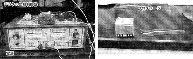
温度制御基板
基板の温度を注意深く制御することができる。例えば、別の態様は、その上に少なくとも1つの先端部材を含む少なくとも1つのカンチレバーと、先端部材上に沈着させた材料とを提供する工程と、材料が先端部材から基板上に沈着して材料沈着物が形成されるようにカンチレバーを基板に接触させる工程とを含み、基板の温度が、材料沈着物のサイズを制御するように適合される、方法を提供する。
Temperature control board The temperature of the board can be carefully controlled. For example, another aspect includes providing at least one cantilever including at least one tip member thereon and a material deposited on the tip member; and the material is deposited on the substrate from the tip member Contacting the cantilever with the substrate such that a deposit is formed, wherein the temperature of the substrate is adapted to control the size of the material deposit.
別の態様は、少なくとも1つのヒートシンクと、少なくとも1つの加熱または冷却ステージと、少なくとも1つの真空システムとを含む装置であって、材料の沈着に供される基板とともに機能し、かつ、沈着の際、基板温度を実質的に一定に保持するように適合した、装置を提供する。 Another aspect is an apparatus that includes at least one heat sink, at least one heating or cooling stage, and at least one vacuum system that functions with and during the deposition of a substrate that is subjected to material deposition. An apparatus adapted to keep the substrate temperature substantially constant.
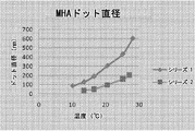
別の態様は、先端部材から基板への材料の沈着速度を、基板に直接取り付けられた装置を用いて基板の温度を制御することによって制御する工程を含む、方法を提供する。基板の温度は、材料沈着物のサイズを制御するように適合することができる。例えば、基板の温度は、25℃未満または25℃を超えるように適合することができる。温度を低くすると、材料沈着物のサイズが減少するかあるいは小さくなり得る。特に、沈着が25℃で行われる場合に、上記サイズに関してサイズを小さくすることができる。例えば、直径または幅を減少させることができる。基板温度は、例えば、20℃未満、または15℃未満、または10℃未満に低下させることができる。温度範囲は、例えば、5℃〜25℃であってもよい。 Another aspect provides a method comprising controlling the deposition rate of material from a tip member to a substrate by controlling the temperature of the substrate using an apparatus attached directly to the substrate. The temperature of the substrate can be adapted to control the size of the material deposit. For example, the temperature of the substrate can be adapted to be less than 25 ° C. or greater than 25 ° C. Lowering the temperature can reduce or reduce the size of the material deposit. In particular, when the deposition is performed at 25 ° C., the size can be reduced with respect to the above size. For example, the diameter or width can be reduced. The substrate temperature can be reduced to, for example, less than 20 ° C., or less than 15 ° C., or less than 10 ° C. The temperature range may be, for example, 5 ° C to 25 ° C.
さらに、一定の温度レベルを実現することができる。例えば、基板の温度は、少なくとも30分間、または少なくとも1時間、または少なくとも5時間、または少なくとも10時間、または少なくとも20時間、または少なくとも48時間、実質的に一定の温度を与えるように適合することができる。 Furthermore, a constant temperature level can be realized. For example, the temperature of the substrate may be adapted to provide a substantially constant temperature for at least 30 minutes, or at least 1 hour, or at least 5 hours, or at least 10 hours, or at least 20 hours, or at least 48 hours. it can.
基板の温度を制御するために装置を用いることができる。例えば、装置は、少なくとも1つのヒートシンク、少なくとも1つの加熱ステージまたは少なくとも1つの冷却ステージ、少なくとも1つの真空システムを含むことができる。真空システムは、基板を保持するために用いることができる。装置は、基板に直接接触することができる。ヒートシンクは、例えば、アルミニウム、銅、または他の金属などの熱伝導性が高い金属を含み得る。ヒートシンクは、積み重ねられたまたは離間した金属ブロックを含むことができ、また、フィンを含むことができる。熱電冷却器または加熱器を使用することができる。ペルチェ素子は当技術分野において公知である。例えば、米国特許第5,171,992号(Claber)および第7,238,294(Koops)を参照されたい。上記装置は、例えば、基板用の環境チャンバとの併用を含むナノリソグラフィ機器との併用に適合させることができる。 An apparatus can be used to control the temperature of the substrate. For example, the apparatus can include at least one heat sink, at least one heating stage or at least one cooling stage, and at least one vacuum system. A vacuum system can be used to hold the substrate. The device can be in direct contact with the substrate. The heat sink can include a metal with high thermal conductivity, such as, for example, aluminum, copper, or other metals. The heat sink can include stacked or spaced metal blocks and can include fins. A thermoelectric cooler or heater can be used. Peltier elements are known in the art. See, for example, US Pat. Nos. 5,171,992 (Claber) and 7,238,294 (Koops). The apparatus can be adapted for use with nanolithographic equipment including, for example, use with an environmental chamber for a substrate.
温度制御をもたらす電圧および電流は、パルス電流または実質的に一定の電流として用いることができる。 The voltages and currents that provide temperature control can be used as pulsed currents or substantially constant currents.
基板の温度は、沈着させた材料が約500nm以下または約100nm以下の横方向寸法を有し得るように適合させることができる。範囲は、例えば、約15nm〜約5ミクロン、または約50nm〜約1ミクロンであってもよい。沈着させた材料はドットまたは線であってもよく、横方向寸法はドット直径または線幅であってもよい。 The temperature of the substrate can be adapted such that the deposited material can have a lateral dimension of about 500 nm or less or about 100 nm or less. The range may be, for example, from about 15 nm to about 5 microns, or from about 50 nm to about 1 micron. The deposited material may be dots or lines and the lateral dimension may be dot diameter or line width.
温度制御を含む試料ステージは、例えば、より小さい金属キャップを上部に有する銅の機械加工片であってもよく、それらの間にTEC(熱電冷却器)がある。上部片は、例えば、内部に埋め込まれたRTDと、真空を用いて試料を定位置に保持することを可能にする上部中央の穴部(whole)とを有している。これらの金属部品は、熱特性が類似した任意の材料で形成することができる。 The sample stage including temperature control may be, for example, a copper machined piece with a smaller metal cap on top, with a TEC (thermoelectric cooler) between them. The upper piece has, for example, an RTD embedded therein and an upper central hole that allows the sample to be held in place using a vacuum. These metal parts can be made of any material with similar thermal properties.
フィンを用いて周囲の空気に対して大きな表面積を提供することによって、冷却モードにおいて試料ステージの下部の熱拡散率を増加させることができる。上部プレートの利用可能表面量は最小となっている。このことにより、高温モードにおいて熱が放射されることおよび冷却モードにおいて冷気が雰囲気温度を吸収することが防止される。このような設計は、エッジおよび試料のすぐ外側の領域を断熱材で覆うことによって利益を得うるであろう。エアロゲルを用いることができる。 By providing a large surface area for the surrounding air using fins, the thermal diffusivity of the lower part of the sample stage can be increased in the cooling mode. The available surface area of the top plate is minimal. This prevents heat from being radiated in the high temperature mode and cold air from absorbing the ambient temperature in the cooling mode. Such a design could benefit from covering the edges and the area just outside the sample with insulation. Airgel can be used.
制御ボックスは、既成のWatlow PID制御器と、RTD温度センサと、12V直流電源と、増幅回路とで構成することができる。2つのNPNトランジスタを用いて増幅器を設計することができる。Watlow制御器の出力は、このような2トランジスタ増幅器を駆動することができる。増幅器は、TEC(熱電冷却器)をほぼ一定の電流で駆動することができ、ノイズの低いステージが提供される。 The control box can be composed of an off-the-shelf Watlow PID controller, an RTD temperature sensor, a 12V DC power supply, and an amplifier circuit. An amplifier can be designed with two NPN transistors. The output of the Watlow controller can drive such a two-transistor amplifier. The amplifier can drive a TEC (thermoelectric cooler) with a nearly constant current, providing a low noise stage.
上記ステージは、加熱および冷却の両方に使用することができる。TECは、加熱のためには高温側を上にして配置し、冷却のためには低温側を上にして配置することができる。 The stage can be used for both heating and cooling. The TEC can be placed with the hot side up for heating and the cold side up for cooling.
均質基板
一態様は、少なくとも1平方ミリメートルの表面積を与える少なくとも1つの表面を含む少なくとも1つの中実基板を含む物品であって、表面が、表面積の少なくとも90%、または少なくとも95%、または少なくとも99%を占める材料沈着物の均質アレイを含む、物品を提供する。材料沈着物が表面積の内側の領域を画定し、材料沈着物の周囲に材料沈着物を含まないエッジ領域が存在し得る。エッジ領域の量は、例えば、表面積の10%以下、または5%以下、または1%以下であり得る。例えば、表面積は、100平方単位であってもよく、表面積の少なくとも90平方単位が、均質沈着物で満たされていてもよい。エッジにある残りの10平方単位は、沈着物を含まなくてもよい。
Homogeneous substrate One aspect is an article comprising at least one solid substrate comprising at least one surface providing a surface area of at least 1 square millimeter, wherein the surface is at least 90%, or at least 95%, or at least 99 of the surface area Articles comprising a homogenous array of material deposits accounting for%. There may be an edge region where the material deposits define a region inside the surface area and no material deposits around the material deposits. The amount of edge region can be, for example, 10% or less, or 5% or less, or 1% or less of the surface area. For example, the surface area may be 100 square units and at least 90 square units of the surface area may be filled with homogeneous deposits. The remaining 10 square units at the edge may not contain deposits.
物品は、少なくとも1つの細胞を表面にさらに含むことができる。 The article can further include at least one cell on the surface.
物品は、材料沈着物の直接描画ナノリソグラフィ印刷を行う工程を含む工程によって準備することができる。 The article can be prepared by a process that includes direct writing nanolithographic printing of material deposits.
別の態様は、少なくとも1平方ミリメートルの表面積を与える少なくとも1つの表面を含む少なくとも1つの中実基板を含む物品であって、表面が、表面積の少なくとも95パーセントを占める材料沈着物の均質アレイを含む、物品を提供する。これは、エッジからエッジまでのパターニングと呼ぶことができる。 Another embodiment is an article comprising at least one solid substrate comprising at least one surface providing a surface area of at least 1 square millimeter, wherein the surface comprises a homogeneous array of material deposits occupying at least 95 percent of the surface area. Provide goods. This can be referred to as edge-to-edge patterning.
別の態様は、少なくとも1平方ミリメートルの表面積を与える少なくとも1つの表面を含む少なくとも1つの中実基板を含む物品であって、表面が、表面積の少なくとも99パーセントを占める材料沈着物の均質アレイを含む、物品を提供する。これは、エッジからエッジまでのパターニングと呼ぶことができる。 Another embodiment is an article comprising at least one solid substrate comprising at least one surface providing a surface area of at least 1 square millimeter, wherein the surface comprises a homogeneous array of material deposits occupying at least 99 percent of the surface area. Provide goods. This can be referred to as edge-to-edge patterning.
一態様では沈着物はドットであり、別の態様では沈着物は線である。 In one aspect, the deposit is a dot, and in another aspect, the deposit is a line.
一態様では、材料沈着物は、実質的に円形の沈着物を含む。 In one aspect, the material deposit includes a substantially circular deposit.
一態様では、材料沈着物は、約1ミクロン未満の平均直径によって特徴付けられる。 In one aspect, the material deposit is characterized by an average diameter of less than about 1 micron.
一態様では、材料沈着物は、約500nm未満の平均直径によって特徴付けられる。 In one aspect, the material deposit is characterized by an average diameter of less than about 500 nm.
一態様では、材料沈着物は、約500nm未満であるが、約50nmより大きい平均直径によって特徴付けられる。 In one aspect, the material deposit is characterized by an average diameter of less than about 500 nm but greater than about 50 nm.
一態様では、材料沈着物は、約1ミクロン未満の平均直径によって特徴付けられる。 In one aspect, the material deposit is characterized by an average diameter of less than about 1 micron.
一態様では、材料沈着物は、中心間で測定された約1ミクロン未満のピッチによって特徴付けられる。 In one aspect, the material deposit is characterized by a pitch of less than about 1 micron measured between centers.
一態様では、材料沈着物は、中心間で測定された約500nm未満のピッチによって特徴付けられる。 In one aspect, the material deposit is characterized by a pitch of less than about 500 nm measured between centers.
一態様では、表面積は少なくとも5平方ミリメートルである。 In one aspect, the surface area is at least 5 square millimeters.
一態様では、表面積は少なくとも10平方ミリメートルである。 In one aspect, the surface area is at least 10 square millimeters.
一態様では、基板は、マーキング表示を含まなくてもよい。例えば、沈着物の行列は、マーキングされる必要はない。 In one aspect, the substrate may not include a marking indication. For example, the deposit matrix need not be marked.
細胞工学
生体細胞および細胞生物学は当技術分野において一般に公知である。例えば、Cell Biology, 2nd Ed., Pollard & Earnshaw, 2008を参照されたい。細胞は、原核細胞または真核細胞であり得る。細胞は、体細胞であり得る。細胞は、全能性細胞、多能性(pluripotent)細胞、多能性(multipotent)細胞、単能性細胞、自己再生可能な細胞、および/または分化可能な細胞であり得る。細胞は、前駆細胞、高分化型(terminally differentiated)細胞などであり得る。本明細書に記載される方法および装置を用いることにより、様々な細胞を調べ、商業利用することができる。
Cell engineering Living cells and cell biology are generally known in the art. See, for example, Cell Biology, 2nd Ed., Pollard & Earnshaw, 2008. The cell can be a prokaryotic cell or a eukaryotic cell. The cell can be a somatic cell. The cells can be totipotent cells, pluripotent cells, multipotent cells, unipotent cells, self-renewable cells, and / or differentiable cells. The cells can be progenitor cells, terminally differentiated cells, and the like. By using the methods and apparatus described herein, various cells can be examined and used commercially.
さらに、幹細胞および幹細胞生物学は当技術分野において一般に公知である。例えば、Essentials of Stem Cell Biology, ed. R. Lanza, 2006; Ferreira et al., Cell Stem Cell 3, August 7, 2008, 136-146を参照されたい。幹細胞の例としては、成体幹細胞および胚性幹細胞;ヒト幹細胞;哺乳類幹細胞;マウス幹細胞;造血幹細胞、神経幹細胞、筋幹細胞;間葉幹細胞;皮膚幹細胞;および胚性幹細胞が挙げられるが、それらに限定されるわけではない。幹細胞は、例えば、肝臓および膵臓を含む異なる器官から採取することができる。一態様では、ヒト胚性幹細胞は、使用可能な幹細胞から除外される。 Furthermore, stem cells and stem cell biology are generally known in the art. See, for example, Essentials of Stem Cell Biology, ed. R. Lanza, 2006; Ferreira et al., Cell Stem Cell 3, August 7, 2008, 136-146. Examples of stem cells include but are not limited to adult stem cells and embryonic stem cells; human stem cells; mammalian stem cells; mouse stem cells; hematopoietic stem cells, neural stem cells, muscle stem cells; mesenchymal stem cells; skin stem cells; It is not done. Stem cells can be taken from different organs including, for example, the liver and pancreas. In one aspect, human embryonic stem cells are excluded from available stem cells.
細胞系統としては、骨形成系統、軟骨形成系統、神経系統、脂肪生成系統、および筋原性系統が含まれるが、それらに限定されるわけではない。 Cell lines include, but are not limited to, osteogenic lines, chondrogenic lines, neural lines, adipogenic lines, and myogenic lines.
幹細胞の増殖および分化を制御するためのインビトロ条件は、当技術分野において公知である。 In vitro conditions for controlling stem cell proliferation and differentiation are known in the art.
組織工学は当技術分野において一般に公知である。例えば、Principles of Tissue Engineering, 2nd Ed., ed. Lanza et al. 2000; Burdick, Tissue Engineering, Vol 14, 00, 2008,1-15を参照されたい。細胞は、二次元環境および三次元環境で成育することができる。 Tissue engineering is generally known in the art. See, for example, Principles of Tissue Engineering, 2nd Ed., Ed. Lanza et al. 2000; Burdick, Tissue Engineering, Vol 14, 00, 2008, 1-15. Cells can be grown in two-dimensional and three-dimensional environments.
パターニングおよび幹細胞分化は、例えば、2008年7月12日に出願された英国仮特許出願第08127899.6号、および2008年9月22日に出願されたCurranらへの米国仮特許出願第61/099,182号に記載されている(2009年7月10日に出願されたPCT/IB2009/006521、および2010年1月14日に出願された米国仮特許出願第61/295,133号も参照されたい)。異なる細胞および幹細胞の例がそれらに記載されている。 Patterning and stem cell differentiation are described, for example, in British Provisional Patent Application No. 08127899.6 filed July 12, 2008, and US Provisional Application No. 61 / 099,182 to Curran et al. (See also PCT / IB2009 / 006521 filed July 10, 2009, and US Provisional Patent Application No. 61 / 295,133 filed January 14, 2010). Examples of different cells and stem cells are described in them.
例えば、細胞(例えば幹細胞を含む)などの他のものとの接点において基板が均質であるような、エッジからエッジまでのパターニングが望ましい。細胞の接着、増殖、および分化は、当技術分野において公知である。例えば、Kong et al., PNAS, March 22,2005, vol. 102, no. 12, 4300-4305; Lee et al., Nano Letters, 2004, 4, 8, 1501-1506を参照されたい。 For example, edge-to-edge patterning is desirable so that the substrate is homogeneous at the point of contact with others such as cells (including, for example, stem cells). Cell attachment, proliferation, and differentiation are known in the art. See, for example, Kong et al., PNAS, March 22,2005, vol. 102, no. 12, 4300-4305; Lee et al., Nano Letters, 2004, 4, 8, 1501-1506.
微細環境における幹細胞は、例えば、Saha et al., Current Opinion in Chemical Biology, 2007, 11, 381-387に記載されている。 Stem cells in a microenvironment are described, for example, in Saha et al., Current Opinion in Chemical Biology, 2007, 11, 381-387.
細胞の接着および成育は、例えば、Arnold et al., ChemPhysChem 2004, 5, 383-388に記載されている。
Cell adhesion and growth are described, for example, in Arnold et al.,
細胞形態、およびナノパターンによって誘発される変化が、例えば、Vim et al., Biomaterials, 2005, 26, 5405-5413に記載されている。 Cell morphology and changes induced by nanopatterns are described, for example, in Vim et al., Biomaterials, 2005, 26, 5405-5413.
実施例
単1D先端部材を用いて様々なインクを金にパターニングするために、DPNパラメータが開発され、制御されてきた。これらの先端部材のための公知のインキングプロセスは、浸漬コーティングである。均質な先端部材コーティングは、均質な構造の製作のためのDPNにおける重要なパラメータである。しかし、先端部材上にチオール結晶が任意に形成されるため、これを浸漬コーティングによって商業的に実現するのは困難であり得る。高スループットおよび大面積製作のため、ペン先端部材の均質なインクコーティングは、2Dペンアレイを用いて実現することができる。先端部材およびシリコン支持体の全体にわたるチオール結晶の架橋、ならびに浸漬および乾燥時に溶媒によって先端部材に生じ得る破損のため、2Dチップは、溶液浸漬コーティングによって被覆することができない。
EXAMPLE DPN parameters have been developed and controlled to pattern various inks into gold using a single 1D tip. A known inking process for these tip members is dip coating. Homogeneous tip coating is an important parameter in DPN for the production of homogeneous structures. However, since thiol crystals are arbitrarily formed on the tip member, this can be difficult to achieve commercially by dip coating. For high throughput and large area fabrication, a uniform ink coating of the pen tip can be achieved using a 2D pen array. Due to the cross-linking of the thiol crystals throughout the tip and silicon support, and the damage that can be caused to the tip by solvents during dipping and drying, the 2D chip cannot be coated by solution dip coating.
実施例1:蒸気コーティング
これらの先端部材を均質に被覆するために、蒸気コーティングに基づく新規な手順がいくつかのチオールインクのために開発された。これらの手順は、固体であればその融点、液体であれば沸点に依存する。真空炉を用いて2Dペンアレイを蒸気コーティングした。先端部材を真空下にて蒸気コーティングすると、チオールインクの融点が所望の作業温度に低下することになる。これは、これらの分子の気相への蒸発を容易にし、これらチオール分子をペン先端部材上に再び凝縮させるために行われた。密閉容器中で、ペンアレイを固体インク材料の真上に配置した。コーティングは、760トルでのチオール化合物の融点に応じて、50〜90℃で行った。コーティングに使用した圧力は300ミリトル未満であった。コーティングプロセスは、プログラム可能な炉を用いた少なくとも2つまたは3つのサイクルを含んでいた。第1のサイクルは、アルミニウム箔で覆われたブリキ容器にチップおよびチオール化合物を装填することを含んでいた。炉室を-300ミリトル以下の圧力に達する(1時間で達し得る)まで排気した。次いで、所望の設定点まで温度を徐々に上昇させた。温度を設定点にて3時間維持した後、6時間かけて徐々に25℃まで冷却した。システムを一晩室温にて放置した。ペン先端部材の均質な被覆を確実にするため全過程を3回繰返した。
Example 1: Vapor Coating In order to coat these tip members homogeneously, a new procedure based on vapor coating was developed for some thiol inks. These procedures depend on the melting point of a solid and the boiling point of a liquid. A 2D pen array was vapor coated using a vacuum oven. If the tip member is vapor coated under vacuum, the melting point of the thiol ink will drop to the desired working temperature. This was done to facilitate the evaporation of these molecules into the gas phase and to condense these thiol molecules back onto the pen tip. In a sealed container, the pen array was placed directly above the solid ink material. Coating was performed at 50-90 ° C. depending on the melting point of the thiol compound at 760 torr. The pressure used for coating was less than 300 millitorr. The coating process included at least two or three cycles using a programmable furnace. The first cycle involved loading a tin container covered with aluminum foil with chips and a thiol compound. The furnace chamber was evacuated until a pressure of -300 millitorr or less was reached (can be reached in 1 hour). The temperature was then gradually increased to the desired set point. The temperature was maintained at the set point for 3 hours and then gradually cooled to 25 ° C over 6 hours. The system was left overnight at room temperature. The entire process was repeated three times to ensure a uniform coating of the pen tip.
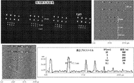
真空下でのサイクリングの他に、必要最低量の所望のチオール化合物を秤量した。この所望の量は、試験を数回行い、チップを被覆するたびに使用量を変えて、2Dペンアレイを均一に被覆するのに必要な平均量を求めることによって決定した。これは、非特異的な沈着を引き起こす過剰な被覆を避けるために行った。上記手順を用いて被覆した二次元ペンアレイの例を図5Aに示す。明るいドットが、x方向において20nm離間してみられ、これは、2つの隣接する先端部材間の距離と同じである。これらのドットは、y方向において90ミクロン離間しており、これは、カンチレバーの全長である。この光学画像に示されるように、ドットは1cm2基板全体にわたって均質に見える。同画像では、基板の一部のみが撮像されている(1100x670平方ミクロンの領域)。 In addition to cycling under vacuum, the required minimum amount of the desired thiol compound was weighed. This desired amount was determined by performing the test several times, changing the amount used each time the chip was coated, and determining the average amount required to uniformly coat the 2D pen array. This was done to avoid excessive coverage that caused non-specific deposition. An example of a two-dimensional pen array coated using the above procedure is shown in FIG. 5A. Bright dots are seen 20 nm apart in the x direction, which is the same as the distance between two adjacent tip members. These dots are 90 microns apart in the y direction, which is the total length of the cantilever. As shown in this optical image, the dots appear uniform across the 1 cm 2 substrate. In this image, only a part of the substrate is imaged (area of 1100 × 670 square microns).
図5Bに示されるように、非均質なドットは非均質なコーティングとなる。光学画像図5Bに示されるように、異なるスポットサイズに加えて、非均質なコーティングならびに先端部材上およびチップ背面における余剰のチオール分子に起因する非特異的な沈着が試料全体にわたって観察される。 As shown in FIG. 5B, non-homogeneous dots result in a non-homogeneous coating. As shown in the optical image FIG. 5B, in addition to the different spot sizes, non-specific deposits due to non-homogeneous coatings and excess thiol molecules on the tip member and on the back of the chip are observed throughout the sample.
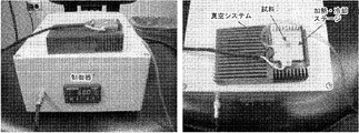
実施例2:レベリング
均質かつ高品質なパターニングを実現するためには、上述の問題を解決しなければならない。上記新規な改良された手順は、2Dナノプリントアレイを基板表面に対していかにしてレベリングするかということ、および全ての先端部材がほぼ同じ負荷で、均等にではあるがほんのわずかだけ表面と接触することをいかにして確実にするかということについて対処するものである。レベリングは、NanoInkのNSCRIPTOR(登録商標)を2D-レベリングユーザインターフェース(同じくNanoInkが開発)と併用して行った。レベリングは2段階で(1つの段階をマクロスケールにて、1つの段階をより精密な光偏向を用いたミクロスケールにて)行った。まず、図6のスキャナのz軸モータを用いて基板に対する2Dチップの平行性を視認することにより、マクロスケールレベリングを行った。この時点では、2Dチップはまだ、表面の数百ミクロン上方にある。第2に、ペンカンチレバーを表面の方へ曲げ、機器の光学系を用いて焦点合わせを行った。この時、レベリングは、レベリングプロトコルと併用した精密な光偏向を用いて行う。カンチレバーの変化をビューポート(図6の挿入図に示すA1-3およびB1-3)を通してモニタリングし、これらの変化をz-モータおよびz-ピエゾによって制御した。
Example 2: Leveling In order to achieve uniform and high-quality patterning, the above-mentioned problems must be solved. The new and improved procedure is how to level the 2D nanoprint array with respect to the substrate surface, and all tip members are in contact with the surface evenly, evenly, with approximately the same load. It deals with how to ensure what is done. Leveling was performed using NanoInk's NSCRIPTOR® together with a 2D-leveling user interface (also developed by NanoInk). Leveling was done in two stages (one stage on a macro scale and one stage on a micro scale using more precise light deflection). First, macroscale leveling was performed by visually confirming the parallelism of the 2D chip with respect to the substrate using the z-axis motor of the scanner of FIG. At this point, the 2D chip is still several hundred microns above the surface. Second, the pen cantilever was bent towards the surface and focused using the instrument's optical system. At this time, leveling is performed using precise light deflection combined with a leveling protocol. Changes in cantilevers were monitored through viewports (A1-3 and B1-3 shown in the inset of FIG. 6) and these changes were controlled by z-motor and z-piezo.
以下の工程を用いて、パターニングされる表面に対して2Dチップをレベリングした。 The 2D chip was leveled against the surface to be patterned using the following steps.
1)シリコン支持構造を通して下にあるカンチレバーを見ることができるビューポート上に光学系の焦点を合わせ、機器上の光学システムを用いて、カンチレバーがレベリングされているか否かを判定する。 1) Focus the optical system onto a viewport where the underlying cantilever can be seen through the silicon support structure and use the optical system on the instrument to determine if the cantilever is leveled.
2)図7のビューポートを通して見えるカンチレバーのアームは緑がかって見え、逆ピラミッド型の先端部材は、2つの赤色ドットをベース上に有している。 2) The cantilever arm seen through the viewport in FIG. 7 appears greenish, and the inverted pyramid tip has two red dots on the base.
3)z-モータを用いて先端部材を表面の数十ミクロン程度上方まで表面に接近させ、光学系を用いて6つのビューポートのいずれかをモニタリングすると、カンチレバーのアームの色に移行(shift)も変化もみられない。 3) When the tip member is brought close to the surface by several tens of microns above the surface using a z-motor and one of the six viewports is monitored using an optical system, it shifts to the color of the cantilever arm. No change is seen.
4)接触前後におけるカンチレバーの外観の変化を図8に示す。先端部材の外観は、図8A、8B、および8Cにそれぞれ示すように、表面上方で異なる状態を経て移動する際、基板表面と最初に接触するとき、およびz-ピエゾが表面との最初の接点を越えて数ミクロン打ち込まれるときに変化する。観察された変化は、カンチレバー端部の2つの赤色のドットにある。カンチレバーが表面の上方にあるときは、2つの明るいドットが見られる(図8A)が、先端部材が表面に接触すると、2つの明るいドットは暗くなり始める(図8B)。この時点で、先端部材は表面にまさに触れ始めている。最終的に、先端部材を表面にさらに深く打ち込むと、2つの赤色のドットは完全に消える。最初の接触から赤色ドットの完全な減光までの位置は、3〜5ミクロンであるが、正確な量はチップによって異なる。この新規なレベリング手順は、「アリゲーターの眼レベリング手法」と呼ぶことができる。理論に限定されるものではないが、2つの赤色ドットは、カンチレバーおよび先端部材の設計ならびに自然光(例えば、レーザ光ではなく)から現れたと思われる。 4) Figure 8 shows changes in the cantilever appearance before and after contact. The appearance of the tip member is as shown in FIGS. 8A, 8B, and 8C, respectively, when moving through different states over the surface, when first contacting the substrate surface, and when the z-piezo is first contacted with the surface It changes when it is driven several microns beyond. The observed change is in the two red dots at the end of the cantilever. When the cantilever is above the surface, two bright dots are seen (Figure 8A), but when the tip is in contact with the surface, the two bright dots begin to darken (Figure 8B). At this point, the tip member is just starting to touch the surface. Eventually, when the tip member is driven deeper into the surface, the two red dots disappear completely. The position from initial contact to complete dimming of the red dot is 3-5 microns, but the exact amount varies from chip to chip. This novel leveling procedure can be referred to as the “Alligator Eye Leveling Technique”. Without being limited to theory, the two red dots appear to have emerged from the cantilever and tip design and from natural light (eg, not laser light).
5)表面と接触する際の各ビューポートにおけるカンチレバーの相対的な眼の減光(eyes-dimming)特性を観察および注目した後、アレイ全体のz全体の位置(z-all position)に着目する。各ビューポートについて、先端部材が表面と接触し、赤色ドットが暗くなったときのz-プローブ値(z-ピエゾの位置から読み取られる)に注目する。これら2つの値を加算し、レベリングソフトウェアに入力する。このプロセスを3つのビューポートについて繰り返す。 5) Observe and pay attention to the relative eye-dimming characteristics of the cantilever in each viewport when in contact with the surface, then focus on the z-all position of the entire array . For each viewport, focus on the z-probe value (read from the z-piezo position) when the tip member contacts the surface and the red dot becomes dark. These two values are added and input to the leveling software. This process is repeated for the three viewports.
6)これらのパラメータをレベリングソフトウェアに入力した後、「レベリング実行」を押し、個々のz軸モーターは、入力されたzプローブ値に基づいてその位置を補正する。この手順を、3つのビューポート間のz-位置における差が1ミクロン未満になるまで繰り返す。 6) After entering these parameters into the leveling software, press “Run Leveling” and each z-axis motor will correct its position based on the input z-probe value. This procedure is repeated until the difference in z-position between the three viewports is less than 1 micron.
7)任意に選択したビューポートを使用して、アレイをz全体の位置で表面に接触させ、カンチレバーが表面に触れるまで1ミクロン未満の増分で最後の接近を行う。全てのビューポートの眼の減光における変化が同じになるまでピエゾを完全に伸長させ、z全体を1ミクロン程後退させる。この時点で、システムはレベリングされ、全ての先端部材が表面に均一に触れており、設計されたリソグラフィアレイを実施することができる。 7) Using an arbitrarily chosen viewport, touch the array to the surface at the entire z position and make a final approach in sub-micron increments until the cantilever touches the surface. Fully extend the piezo until the same change in dimming of the eyes in all viewports is the same, and retract the entire z by 1 micron. At this point, the system is leveled and all tip members touch the surface evenly, and the designed lithographic array can be implemented.
8)この手法を用いて、最初の接触後の100nm〜数ミクロンの範囲の最初のz位置から完全な眼の減光により、優れたリソグラフィを均一な接触および均質な製作とともにもたらすことができる。しかし、接触前に眼が完全に赤色であると、2Dペンアレイはドットを全くパターニングできない場合がある。眼が完全に減光して赤色ドットが消え、先端部材がさらに基板中に押し込まれると、図1に示すようにカンチレバーの背面に偏向が生じ始め、これが歪んだパターニングにつながることになる。 8) Using this approach, excellent lithography can be provided with uniform contact and uniform fabrication with full eye dimming from the first z position in the range of 100 nm to several microns after the initial contact. However, if the eye is completely red before contact, the 2D pen array may not be able to pattern the dots at all. When the eye is completely dimmed and the red dot disappears and the tip member is pushed further into the substrate, the back surface of the cantilever begins to deflect as shown in FIG. 1, which leads to distorted patterning.
9)レベリングの後、設計されたパターンが実施され、先端部材はどのビューポートから見ても表面に出入りする際に点滅し始める(赤色の眼は接触無し、薄暗い眼は接触中)。 9) After leveling, the designed pattern is implemented and the tip member begins to flash as it enters and exits the surface from any viewport (red eyes are not touching, dim eyes are touching).
10)レベリングの他に、試料保持器上に試料を載置する際に十分な注意を払わなければならない。試料の背面には、システムのレベリングを困難にするであろういかなるごみも微小な異物も存在してはならない。これは、試料保持器および基板の背面をアセトンなどの有機溶媒で拭いた後、空気乾燥または窒素乾燥を行うことで実現することができる。 10) In addition to leveling, sufficient care must be taken when placing the sample on the sample holder. The back of the sample should be free of any debris and small foreign objects that will make system leveling difficult. This can be realized by performing air drying or nitrogen drying after wiping the back surface of the sample holder and the substrate with an organic solvent such as acetone.
11)基板は、ビューポート2および3に対して中心に位置決めされる必要がある。 11) The substrate needs to be centered with respect to viewports 2 and 3.
12)チオールインクの異なる種類ごとに異なるDPN環境条件を用いなければならない。 12) Different DPN environmental conditions must be used for different types of thiol inks.
13)2Dペンアレイがシステム上でレベリングされると、若干の試料間のレベリングを行うことで、異なる試料を同時に製作することができる。 13) When the 2D pen array is leveled on the system, different samples can be manufactured simultaneously by leveling between some samples.
このレベリング技術は、基板に対して2Dチップをレベリングするための高速かつ正確な方法を提供し、これにより、カンチレバーと表面との間の均一な接触がもたらされ、大型基板全体に再現可能で、正確かつ均質なパターニングが実現されるであろう。 This leveling technology provides a fast and accurate way to level the 2D chip against the substrate, which results in uniform contact between the cantilever and the surface and is reproducible across large substrates. Accurate and uniform patterning will be realized.
図9は、5mm2の試料のエッジからエッジまでのパターニングの例を示し、この光学顕微鏡画像(製作後のエッチングされた5mm2金基板を示す)に示される領域全体にわたって均質なドットが製作され、領域全体にわたる均一かつおよび均質な4x6ドットアレイとなる。製作された基板の四隅の構造の均質性を示す部分である。 Figure 9 shows an example of edge-to-edge patterning of a 5mm 2 sample, where uniform dots are produced over the entire area shown in this optical microscope image (showing an etched 5mm 2 gold substrate after fabrication). A uniform and homogeneous 4x6 dot array over the entire area. It is a part showing the homogeneity of the structure of the four corners of the manufactured substrate.
図10は、4行および12列のドットからなるアレイの高分解能光学画像を示し、赤色の枠で囲んだ領域において、上部から下部へと向かって3列ごとに、異なる滞留時間(それぞれ、10秒、5秒、1秒、0.1秒)で製作されたドットからなる。図示されるように、これらのドットは、同じ列および行にわたって、またアレイ間で均質である。各アレイの始まりにおいて、第1の接触点に関連する1つのドットが存在する。これらの光学画像に示されるように、変形、スキューイング、非特異的な沈着、およびネガティブ形状は存在せず、全てのアレイがはっきりと確定され、まっすぐで、鮮明である。 FIG. 10 shows a high-resolution optical image of an array of 4 rows and 12 columns of dots, with different residence times (10 and 10 respectively) for each of the three columns from the top to the bottom in the red boxed area. Seconds, 5 seconds, 1 second, 0.1 seconds). As shown, these dots are uniform across the same columns and rows and between arrays. At the beginning of each array, there is one dot associated with the first contact point. As shown in these optical images, there is no deformation, skewing, non-specific deposition, and negative shape, and all arrays are clearly defined, straight, and sharp.
1Dプローブアレイパターニングと同様に、ドットのピッチおよびサイズは、2Dペンアレイを用いて制御することができる。図11は、アリゲーターの眼レベリング後に得られたパターニングの例を示す。図11Aの光学画像(50倍)は、1μm離間したナノドットからなる矩形アレイを示し、このスケールでは、形状は顕微鏡の分解能未満であるため、これら形状を解像することができなかった。図11Bおよび図11Cは、平均ドット直径が90nmである製作されたドットアレイの構造的AFM画像および線プロファイルを示す。この高精度レベリング技術は、2Dペンアレイを基板に対してレベリングするための高速、正確、かつ再現可能なプロトコルを提供し、その結果、高品質かつ均質なパターニングが大型基板全体にわたって得られた。 Similar to 1D probe array patterning, dot pitch and size can be controlled using a 2D pen array. FIG. 11 shows an example of patterning obtained after eye leveling of the alligator. The optical image (50x) in FIG. 11A shows a rectangular array of nanodots spaced 1 μm apart, and at this scale, the shapes were below the resolution of the microscope and could not be resolved. FIGS. 11B and 11C show structural AFM images and line profiles of fabricated dot arrays with an average dot diameter of 90 nm. This high-accuracy leveling technology provides a fast, accurate, and reproducible protocol for leveling 2D pen arrays to the substrate, resulting in high quality and uniform patterning across large substrates.
実施例4:温度制御によるDPN印刷を用いた金基板上のチオール分子の拡散率制御
幹細胞分化のためのDPNおよび2Dペンアレイを用いて金基板上にチオール化した分子ナノ構造の製作を成功させるためには、いくつかの問題に対処する必要がある。基板全体にわたる均質なスポット直径、スポット直径を100nm未満に再現すること、再現可能なプロトコル、チオール化した分子の拡散の制御(拡散の減速または高速化)、および非特異的な沈着を最小限にすること、といった重要なパラメータは、均質な幹細胞分化を実現するために対処する必要がある非常に重要な問題である。これらの問題は、チオール化した被覆先端部材および基板システムの加熱または冷却を可能にする加熱・冷却ステージを用いることにより対処することができる。
Example 4: Controlling diffusivity of thiol molecules on a gold substrate using temperature controlled DPN printing To successfully fabricate thiolated molecular nanostructures on a gold substrate using DPN and 2D pen arrays for stem cell differentiation There are several issues that need to be addressed. Homogeneous spot diameter across the substrate, reproducible spot diameter below 100 nm, reproducible protocol, controlled diffusion of thiolated molecules (diffusion slowing or speeding up), and minimizing non-specific deposition Important parameters such as to do are very important issues that need to be addressed in order to achieve homogeneous stem cell differentiation. These problems can be addressed by using heating and cooling stages that allow heating or cooling of the thiolated coated tip and substrate system.
第1世代:
従来、時折問題になっていたのは、限定されるわけではないが、ODT(1オクタデカンチオール)、HDT(1-ヘキサデカンチオール)、およびMUD(11-メルカプト-1-ウンデカノール)といった多くの低融点チオール分子が被覆2Dペンアレイから高速に拡散するということであった。これら分子は、室温で高速拡散し、これにより、被覆先端部材と金基板との間の接触点を必要最小限に(滞留時間0.01秒)にしても100nmより大きいナノ構造が製作される場合が多かった。この問題を回避するため、本発明者らは、基板を冷却する冷却ステージを設計した。冷却システムは、電源と、熱電冷却器または加熱器とも呼ばれるペルチェモジュールを伴うステージとしてのアルミニウムの固体ブロックと、回路基板と、デジタル加熱制御器とで構成される。パルス的に電圧を印加することにより、アルミニウム製ステージおよび基板を10℃未満に冷却することができる。図12は、この設計の構成要素を示す。
First generation:
Many low melting points, such as, but not limited to, ODT (1 octadecanethiol), HDT (1-hexadecanethiol), and MUD (11-mercapto-1-undecanol), which have traditionally been an occasional problem It was that thiol molecules would diffuse rapidly from the coated 2D pen array. These molecules diffuse rapidly at room temperature, which can produce nanostructures larger than 100 nm, even if the contact point between the coated tip and the gold substrate is minimized (residence time 0.01 seconds). There were many. In order to avoid this problem, the present inventors designed a cooling stage for cooling the substrate. The cooling system consists of a power source, a solid block of aluminum as a stage with a Peltier module, also called a thermoelectric cooler or heater, a circuit board, and a digital heating controller. By applying the voltage in a pulsed manner, the aluminum stage and the substrate can be cooled to less than 10 ° C. FIG. 12 shows the components of this design.
第1世代冷却システムは、生成されたパターンのドット直径形状を減少させることができたものの、いくつかの問題を有していた。ステージの冷却が連続的または可変制御的にではなくパルスモードで行われていたため、パターン製作の際にノイズが生じた。さらに、温度が数分しか16℃未満に維持されず、製作および画像化の際にドリフティングが起こった。興味深いことに、雰囲気温度未満の温度である約18℃では、先端部材から基板表面へのチオール分子の拡散率は遅くなり、図2に示されるように、生成されたドットの直径は小さくなっていた。25℃および18℃における滞留時間5秒での構造的AFM(TAFM)画像のスポット直径は、それぞれ、460nmおよび256nmである。ODT被覆先端部材を用いてこれらのアレイを金薄膜上に製作し、製作された基板を金エッチング剤を用いてエッチングした後、AFM画像化を行った。さらに、図13Aおよび13Bに示されるように、両アレイは、図13Aでは右、13Bでは左に歪んでいるが、これは、冷却システムが所望の温度を維持することができないためである。 Although the first generation cooling system was able to reduce the dot diameter shape of the generated pattern, it had several problems. Since the stage was cooled not in a continuous or variable control but in a pulse mode, noise was generated during pattern fabrication. In addition, the temperature was maintained below 16 ° C. for only a few minutes and drifting occurred during fabrication and imaging. Interestingly, at a temperature below the ambient temperature of about 18 ° C, the diffusivity of thiol molecules from the tip member to the substrate surface is slow, and the diameter of the generated dots is reduced, as shown in Figure 2. It was. The spot diameters of structural AFM (TAFM) images with a residence time of 5 seconds at 25 ° C. and 18 ° C. are 460 nm and 256 nm, respectively. These arrays were fabricated on a gold thin film using an ODT-coated tip member, and the fabricated substrate was etched using a gold etchant, and then AFM imaging was performed. In addition, as shown in FIGS. 13A and 13B, both arrays are distorted to the right in FIG. 13A and to the left in 13B because the cooling system cannot maintain the desired temperature.
第2世代:
第1世代冷却ステージに付随する固有の問題のため、第2世代が開発された。連続電流フローを用いる第2世代は、第1の設計と比較して大幅な改善であった。なぜなら、より長時間(約40分)一定の温度を保持することができたからである。この新たに設計されたステージは、図14に示されるような、積み重ねられ、各ブロックが5mm離間したアルミニウムブロックであった。ブロックにおける間隔により、空気が入り込んで熱伝達を起こすことが可能となる。
Second generation:
Due to the inherent problems associated with the first generation cooling stage, the second generation was developed. The second generation using continuous current flow was a significant improvement over the first design. This is because a constant temperature could be maintained for a longer time (about 40 minutes). The newly designed stage was an aluminum block that was stacked and blocks separated by 5 mm, as shown in FIG. The spacing in the blocks allows air to enter and cause heat transfer.
第1世代冷却ステージによる結果と同様に、この新たな設計は、システムを冷却し、生成されるドットの直径を減少させることが可能であった。構造的AFM画像および輪郭プロットは、温度の減少に伴ってドット直径形状の減少が観察されることを示している(図15)。滞留時間を4秒にすると、ドット直径は、28℃で製作されたときの610nmから10℃で82nmに減少し、これは慣例的に(routinely)製作が可能である。第1世代冷却システムを用いてこのサイズを実現するのは困難であった。さらに、より早い滞留時間(0.4秒)にすると、慣例的に直径形状を35nmにさらに減少することができる。興味深いことに、滞留時間および温度の両方についてほぼ直線的な関係が観察される(図16)。(2つの異なるOTである4秒および0.4秒でのMHAのR2は、それぞれ、0.948および0.971である)。 Similar to the results from the first generation cooling stage, this new design was able to cool the system and reduce the diameter of the dots produced. Structural AFM images and contour plots show that a decrease in dot diameter shape is observed with decreasing temperature (Figure 15). With a dwell time of 4 seconds, the dot diameter decreases from 610 nm when fabricated at 28 ° C. to 82 nm at 10 ° C., which can be routinely fabricated. It was difficult to achieve this size using the first generation cooling system. Furthermore, with a faster residence time (0.4 seconds), the diameter shape can conventionally be further reduced to 35 nm. Interestingly, a nearly linear relationship is observed for both residence time and temperature (Figure 16). (The R2 of MHA at 2 different OTs, 4 and 0.4 seconds, is 0.948 and 0.971, respectively).
生成されるドット直径形状に対する温度の影響が他のチオール化した分子にも適用可能であるか否かを確認するため、1-オクタデカンチオールをインクとして使用し、描画温度を16-メルカプトヘキサデカンチオールのものと同様に変化させた。描画温度20.9℃および16℃について、158nmから40nmまでのドット直径形状の減少が観察された。温度に対してドット直径形状をプロットしたところ、0.9998のR2値が得られた。 To see if the effect of temperature on the generated dot diameter shape is applicable to other thiolated molecules, 1-octadecanethiol was used as the ink and the drawing temperature was adjusted to that of 16-mercaptohexadecanethiol. Changed as well. For drawing temperatures 20.9 ° C. and 16 ° C., a decrease in dot diameter shape from 158 nm to 40 nm was observed. When the dot diameter shape was plotted against temperature, an R2 value of 0.9998 was obtained.
第3世代:
1mm2以上の範囲の大規模パターニングを行う際、滞留時間を最小限とすることが2つの理由から重要である。1つには、最大スループットを得るために、エッジからエッジまでの描画時間を高速化すること、および製作時間(望ましくは2時間未満)にわたって非特異的な沈着を回避することであり、熱ドリフトが起こることなく第2世代を用いて達成することができた最大描画時間は40分であり、これは、ドット間のピッチが280nm以下である高密度アレイを製作するには不十分である。そのため、新規なステージ設計および材料により、ドリフティングを起こすことなく温度を数十時間一定に保持する冷却・加熱ステージとして第3世代が設計された。図18は、加熱・冷却システムを示す。熱放散のために銅が使用され、ヒートシンクは多数のフィンおよび大きい表面積を有している。真空システムが基板を保持する。
3rd generation:
Minimizing dwell time is important for two reasons when performing large-scale patterning over 1 mm2. One is to speed up the drawing time from edge to edge for maximum throughput and to avoid non-specific deposition over the production time (preferably less than 2 hours) and thermal drift The maximum writing time that could be achieved using the second generation without any occurrence was 40 minutes, which is insufficient to produce a high density array with a dot-to-dot pitch of 280 nm or less. Therefore, the third generation was designed as a cooling and heating stage that keeps the temperature constant for several tens of hours without causing drifting by using a new stage design and materials. FIG. 18 shows a heating / cooling system. Copper is used for heat dissipation and the heat sink has a large number of fins and a large surface area. A vacuum system holds the substrate.
ODT被覆2Dペンアレイおよび新規な冷却システムを用いて製作された滞留時間の異なるドットのアレイの例が図19に示されている。 An example of an array of dots with different residence times produced using an ODT coated 2D pen array and a novel cooling system is shown in FIG.
融点がより高いチオール分子は、低融点チオール分子ほど容易には先端部材から基板表面へ拡散しないため、必要最小限の滞留時間で拡散率を増加させる異なる構成が必要である。一例として、アミン官能基を有するチオール分子(1-アミノウンデカンチオール(AUT))を用い、温度を増加させることによって拡散率が増加するか否かを検査した。図20は、1つの先端部材を使用して、異なる温度で様々な滞留時間を用いて製作されたAUTナノ構造の摩擦AFM画像を示す。これらの画像に示されるように、温度を増加させると、生成されるスポット直径が増加する。さらに、図20Cおよび20Dに示すように、スポット直径は湿度の増加とともに増加した。 Since thiol molecules with higher melting points do not diffuse from the tip member to the substrate surface as easily as low melting point thiol molecules, a different configuration is required that increases the diffusivity with the minimum required residence time. As an example, a thiol molecule having an amine functional group (1-aminoundecanethiol (AUT)) was used to examine whether the diffusivity was increased by increasing the temperature. FIG. 20 shows friction AFM images of AUT nanostructures fabricated using a single tip member with different residence times at different temperatures. As shown in these images, increasing the temperature increases the spot diameter produced. Furthermore, as shown in FIGS. 20C and 20D, the spot diameter increased with increasing humidity.
同一アレイでの先端部材ごとの、生成されたスポットのアレイ均質性を検査するため、本発明者らは、真空下での蒸気コーティングを用いてAUTで被覆した52個の先端部材からなる10ペンアレイを使用した。図21に示されるように、光学暗視野顕微鏡検査およびAFM摩擦画像は、同一のアレイおよび滞留時間が同じアレイ間においてスポット直径の変化を示さなかった。これらのアレイは、60℃および相対湿度65%にて製作された。さらに、滞留時間を減少させると、10秒から0.1秒について、それぞれ、460nmから74nmに減少した。カーソルプロファイルは、ドット直径の減少を示している。 In order to check the array homogeneity of the generated spots for each tip member in the same array, we have a 10-pen array consisting of 52 tip members coated with AUT using vapor coating under vacuum. It was used. As shown in FIG. 21, optical dark field microscopy and AFM friction images showed no change in spot diameter between the same array and dwell time. These arrays were made at 60 ° C. and 65% relative humidity. Furthermore, when the residence time was decreased, the time decreased from 460 nm to 74 nm for 10 seconds to 0.1 seconds, respectively. The cursor profile shows a decrease in dot diameter.
スループットをより高めるため、真空下にて2DペンアレイをAUTで蒸気コーティングした。図22に示すように、エッジからエッジまでの均質なアレイを60℃にて5mm2基板上に生成した。沈着の制御を向上させ、レベリング中またはパターン実施前の第1の接触点を無くすため、ステージを低温で作動させて所望のチオールの拡散を著しく減速させた。これにより、本発明者らは、パターニングの前に沈着を一切起こすことなくあるいは最小限の沈着でレベリングおよび接近を行うことが可能になり、最初の接近ドットを無くし得る。場合によっては、熱変化によってステージが拡張または縮小し、金属の拡張によって元のz-高さ(先端部材と表面との接点)に差が生じ得る。このような変化は、z-ピエゾに作用する電圧を所望のパターンを得るために増加または減少させることによって補償することができる。 To further increase the throughput, 2D pen arrays were vapor coated with AUT under vacuum. A homogeneous array from edge to edge was produced on a 5 mm 2 substrate at 60 ° C. as shown in FIG. To improve deposition control and eliminate the first contact point during leveling or before patterning, the stage was operated at low temperature to significantly slow down the desired thiol diffusion. This allows us to level and approach with no or minimal deposition prior to patterning and eliminate the first approaching dot. In some cases, thermal changes cause the stage to expand or contract, and metal expansion can cause differences in the original z-height (contact between the tip member and the surface). Such changes can be compensated by increasing or decreasing the voltage acting on the z-piezo to obtain the desired pattern.
実施例5:間葉幹細胞応答に対する均質表面の効果
ディップペン・ナノリソグラフィを使用し、ナノメートルスケールで沈着させたメチル基を有するチオール化したインク(ODT)を用いて5mm2の均質なナノパターンを金の表面に2Dナノプリントアレイで作製した。ナノパターンは、280nmの固定距離(ピッチ、dα)および固定直径(dβ約65〜70nm)だけ離間した一連の並行ドットで構成されていた。Lonza社から入手した細胞を4つの経路に通し、24ウェルプレート中で、1mLの基本培地(Lonza社、間充織細胞成育培地)を用いて1つのウェルにつき50,000個の細胞の濃度でODT基板に接触させた状態で培養した。
Example 5: Effect of homogeneous surface on mesenchymal
試料を、間葉幹細胞マーカーである、STRO-1およびヌクレオステミン、ならびに核(DAPI)およびアクチン繊維に対して染色した。試料をODT基板上に配置し、蛍光安定化封入剤であるVectashieldで封入した。試料をZeiss社の機種であるAxio imager顕微鏡で分析した。図23および図24を参照されたい。 Samples were stained for mesenchymal stem cell markers, STRO-1 and nucleostemin, as well as nucleus (DAPI) and actin fibers. Samples were placed on an ODT substrate and encapsulated with Vectashield, a fluorescent stabilized encapsulant. Samples were analyzed with an Axio imager microscope, a model of Zeiss. See FIG. 23 and FIG.
TissueGnostic(商標)分析は、各細胞が、間葉幹細胞マーカーであるSTRO-1およびヌクレオステミンの両方を発現したことを示した。細胞形態および間葉幹細胞マーカーの発現から、これらの結果は、応答がODT基板全体にわたって均質であったことを示している。 TissueGnostic ™ analysis indicated that each cell expressed both the mesenchymal stem cell markers STRO-1 and nucleostemin. From cell morphology and expression of mesenchymal stem cell markers, these results indicate that the response was homogeneous across the ODT substrate.
Claims (21)
Applications Claiming Priority (3)
| Application Number | Priority Date | Filing Date | Title |
|---|---|---|---|
| US14745209P | 2009-01-26 | 2009-01-26 | |
| US61/147,452 | 2009-01-26 | ||
| PCT/US2010/022015 WO2010085769A1 (en) | 2009-01-26 | 2010-01-25 | Large area, homogeneous array fabrication including homogeneous substrates |
Publications (2)
| Publication Number | Publication Date |
|---|---|
| JP2012515560A true JP2012515560A (en) | 2012-07-12 |
| JP2012515560A5 JP2012515560A5 (en) | 2013-03-14 |
Family
ID=42096549
Family Applications (1)
| Application Number | Title | Priority Date | Filing Date |
|---|---|---|---|
| JP2011548194A Pending JP2012515560A (en) | 2009-01-26 | 2010-01-25 | Manufacturing method of large area homogeneous array including homogeneous substrate |
Country Status (8)
| Country | Link |
|---|---|
| US (1) | US20100221505A1 (en) |
| EP (1) | EP2389614A1 (en) |
| JP (1) | JP2012515560A (en) |
| KR (1) | KR20110124214A (en) |
| AU (1) | AU2010206594A1 (en) |
| CA (1) | CA2750430A1 (en) |
| SG (1) | SG172852A1 (en) |
| WO (1) | WO2010085769A1 (en) |
Families Citing this family (5)
| Publication number | Priority date | Publication date | Assignee | Title |
|---|---|---|---|---|
| JP2012515559A (en) * | 2009-01-26 | 2012-07-12 | ナノインク インコーポレーティッド | Fabrication method for large area homogeneous arrays including controlled tip load deposition |
| US8214916B2 (en) * | 2009-01-26 | 2012-07-03 | Nanoink, Inc. | Large area, homogeneous array fabrication including leveling with use of bright spots |
| US9040339B2 (en) | 2013-10-01 | 2015-05-26 | The Pen | Practical method of producing an aerogel composite continuous thin film thermoelectric semiconductor material |
| US9276190B2 (en) | 2013-10-01 | 2016-03-01 | The Pen | Practical method of producing an aerogel composite continuous thin film thermoelectric semiconductor material by modified MOCVD |
| EP4003683A1 (en) * | 2019-07-23 | 2022-06-01 | University Of Massachusetts | Thermal imprinting of nanostructure materials |
Citations (3)
| Publication number | Priority date | Publication date | Assignee | Title |
|---|---|---|---|---|
| WO2007126689A1 (en) * | 2006-04-19 | 2007-11-08 | Northwestern University | Article for parallel lithography with two-dimensional pen arrays |
| WO2008091279A2 (en) * | 2006-06-28 | 2008-07-31 | Northwestern University | Etching and hole arrays |
| WO2008112713A1 (en) * | 2007-03-13 | 2008-09-18 | Nanoink, Inc. | Nanolithography with use of viewports |
Family Cites Families (26)
| Publication number | Priority date | Publication date | Assignee | Title |
|---|---|---|---|---|
| USRE23838E (en) | 1950-09-14 | 1954-06-08 | Post-deflected color kinescope | |
| US5171992A (en) * | 1990-10-31 | 1992-12-15 | International Business Machines Corporation | Nanometer scale probe for an atomic force microscope, and method for making same |
| US6635311B1 (en) * | 1999-01-07 | 2003-10-21 | Northwestern University | Methods utilizing scanning probe microscope tips and products therefor or products thereby |
| US6827979B2 (en) * | 1999-01-07 | 2004-12-07 | Northwestern University | Methods utilizing scanning probe microscope tips and products therefor or produced thereby |
| US7291284B2 (en) | 2000-05-26 | 2007-11-06 | Northwestern University | Fabrication of sub-50 nm solid-state nanostructures based on nanolithography |
| US6642129B2 (en) | 2001-07-26 | 2003-11-04 | The Board Of Trustees Of The University Of Illinois | Parallel, individually addressable probes for nanolithography |
| SE0102764D0 (en) | 2001-08-17 | 2001-08-17 | Astrazeneca Ab | Compounds |
| AU2003211027A1 (en) | 2002-03-27 | 2003-10-13 | Nanoink, Inc. | Method and apparatus for aligning patterns on a substrate |
| US7060977B1 (en) | 2002-05-14 | 2006-06-13 | Nanoink, Inc. | Nanolithographic calibration methods |
| EP1363164B1 (en) * | 2002-05-16 | 2015-04-29 | NaWoTec GmbH | Procedure for etching of materials at the surface with focussed electron beam induced chemical reactions at said surface |
| WO2004044552A2 (en) * | 2002-11-12 | 2004-05-27 | Nanoink, Inc. | Methods and apparatus for ink delivery to nanolithographic probe systems |
| US20040228962A1 (en) | 2003-05-16 | 2004-11-18 | Chang Liu | Scanning probe microscopy probe and method for scanning probe contact printing |
| EP1748846B1 (en) | 2004-04-30 | 2015-04-01 | Bioforce Nanosciences, Inc. | Method and apparatus for depositing material onto a surface |
| JP4649416B2 (en) * | 2004-10-29 | 2011-03-09 | 独立行政法人科学技術振興機構 | MALDI-TOFMS substrate and mass spectrometry method using the same |
| EP1846249A2 (en) | 2005-01-10 | 2007-10-24 | Bioforce Nanosciences, Inc. | Topographically indexed support substrates |
| US8256017B2 (en) * | 2006-08-31 | 2012-08-28 | Nanoink, Inc. | Using optical deflection of cantilevers for alignment |
| JP2010530126A (en) * | 2006-12-18 | 2010-09-02 | ノースウエスタン ユニバーシティ | Manufacturing method of microstructure and nano structure using etching resist |
| CA2681443A1 (en) * | 2007-05-09 | 2008-11-20 | Nanoink, Inc. | Compact nanofabrication apparatus |
| AU2008284284A1 (en) * | 2007-08-08 | 2009-02-12 | Northwestern University | Independently-addressable, self-correcting inking for cantilever arrays |
| JP2011513945A (en) * | 2008-02-05 | 2011-04-28 | ナノインク インコーポレーティッド | Array and cantilever array leveling methods |
| EP2283395B1 (en) | 2008-04-25 | 2018-08-22 | Northwestern University | Polymer pen lithography |
| GB0812789D0 (en) * | 2008-07-12 | 2008-08-20 | Univ Liverpool | Materials and methods for cell growth |
| US8214916B2 (en) * | 2009-01-26 | 2012-07-03 | Nanoink, Inc. | Large area, homogeneous array fabrication including leveling with use of bright spots |
| JP2012515559A (en) * | 2009-01-26 | 2012-07-12 | ナノインク インコーポレーティッド | Fabrication method for large area homogeneous arrays including controlled tip load deposition |
| SG172853A1 (en) * | 2009-01-26 | 2011-08-29 | Nanoink Inc | Large area, homogeneous array fabrication including substrate temperature control |
| US9918209B2 (en) | 2013-10-28 | 2018-03-13 | Microsoft Technology Licensing, Llc | Policies for selecting sources for resource strings |
-
2010
- 2010-01-25 US US12/656,310 patent/US20100221505A1/en not_active Abandoned
- 2010-01-25 WO PCT/US2010/022015 patent/WO2010085769A1/en active Application Filing
- 2010-01-25 SG SG2011048980A patent/SG172852A1/en unknown
- 2010-01-25 JP JP2011548194A patent/JP2012515560A/en active Pending
- 2010-01-25 KR KR1020117017435A patent/KR20110124214A/en not_active Application Discontinuation
- 2010-01-25 AU AU2010206594A patent/AU2010206594A1/en not_active Abandoned
- 2010-01-25 CA CA2750430A patent/CA2750430A1/en not_active Abandoned
- 2010-01-25 EP EP10702949A patent/EP2389614A1/en not_active Withdrawn
Patent Citations (3)
| Publication number | Priority date | Publication date | Assignee | Title |
|---|---|---|---|---|
| WO2007126689A1 (en) * | 2006-04-19 | 2007-11-08 | Northwestern University | Article for parallel lithography with two-dimensional pen arrays |
| WO2008091279A2 (en) * | 2006-06-28 | 2008-07-31 | Northwestern University | Etching and hole arrays |
| WO2008112713A1 (en) * | 2007-03-13 | 2008-09-18 | Nanoink, Inc. | Nanolithography with use of viewports |
Also Published As
| Publication number | Publication date |
|---|---|
| AU2010206594A1 (en) | 2011-07-28 |
| EP2389614A1 (en) | 2011-11-30 |
| WO2010085769A1 (en) | 2010-07-29 |
| SG172852A1 (en) | 2011-08-29 |
| CA2750430A1 (en) | 2010-07-29 |
| KR20110124214A (en) | 2011-11-16 |
| US20100221505A1 (en) | 2010-09-02 |
Similar Documents
| Publication | Publication Date | Title |
|---|---|---|
| EP2013662B1 (en) | Article for parallel lithography with two-dimensional pen arrays | |
| JP2010521325A (en) | Nanolithography using viewport | |
| JP2012516064A (en) | Fabrication method of large area homogeneous array including substrate temperature control | |
| Tseng | Advancements and challenges in development of atomic force microscopy for nanofabrication | |
| KR101291671B1 (en) | Thermal control of deposition in dip pen nanolithography | |
| US8214916B2 (en) | Large area, homogeneous array fabrication including leveling with use of bright spots | |
| US8256018B2 (en) | Array and cantilever array leveling | |
| JP2012515559A (en) | Fabrication method for large area homogeneous arrays including controlled tip load deposition | |
| WO2009140440A1 (en) | Dual-tip cantilever | |
| JP2012515560A (en) | Manufacturing method of large area homogeneous array including homogeneous substrate | |
| US20110014378A1 (en) | Leveling devices and methods | |
| Haaheim et al. | Self‐leveling two‐dimensional probe arrays for Dip Pen Nanolithography® | |
| CN110534257A (en) | A kind of accurate production method of microelectrode of thermo-labile dimensional thinlayer material | |
| WO2012026927A1 (en) | Leveling devices and methods |
Legal Events
| Date | Code | Title | Description |
|---|---|---|---|
| A521 | Written amendment |
Free format text: JAPANESE INTERMEDIATE CODE: A523 Effective date: 20130124 |
|
| A621 | Written request for application examination |
Free format text: JAPANESE INTERMEDIATE CODE: A621 Effective date: 20130124 |
|
| A977 | Report on retrieval |
Free format text: JAPANESE INTERMEDIATE CODE: A971007 Effective date: 20140117 |
|
| A131 | Notification of reasons for refusal |
Free format text: JAPANESE INTERMEDIATE CODE: A131 Effective date: 20140203 |
|
| A02 | Decision of refusal |
Free format text: JAPANESE INTERMEDIATE CODE: A02 Effective date: 20140625 |