JP2012514319A - Semiconductor device metallization system with specially tapered transition vias - Google Patents
Semiconductor device metallization system with specially tapered transition vias Download PDFInfo
- Publication number
- JP2012514319A JP2012514319A JP2011542726A JP2011542726A JP2012514319A JP 2012514319 A JP2012514319 A JP 2012514319A JP 2011542726 A JP2011542726 A JP 2011542726A JP 2011542726 A JP2011542726 A JP 2011542726A JP 2012514319 A JP2012514319 A JP 2012514319A
- Authority
- JP
- Japan
- Prior art keywords
- via opening
- opening
- mask
- dielectric material
- etching
- Prior art date
- Legal status (The legal status is an assumption and is not a legal conclusion. Google has not performed a legal analysis and makes no representation as to the accuracy of the status listed.)
- Pending
Links
Images


Classifications
-
- H—ELECTRICITY
- H01—ELECTRIC ELEMENTS
- H01L—SEMICONDUCTOR DEVICES NOT COVERED BY CLASS H10
- H01L21/00—Processes or apparatus adapted for the manufacture or treatment of semiconductor or solid state devices or of parts thereof
- H01L21/70—Manufacture or treatment of devices consisting of a plurality of solid state components formed in or on a common substrate or of parts thereof; Manufacture of integrated circuit devices or of parts thereof
- H01L21/71—Manufacture of specific parts of devices defined in group H01L21/70
- H01L21/768—Applying interconnections to be used for carrying current between separate components within a device comprising conductors and dielectrics
- H01L21/76801—Applying interconnections to be used for carrying current between separate components within a device comprising conductors and dielectrics characterised by the formation and the after-treatment of the dielectrics, e.g. smoothing
- H01L21/76802—Applying interconnections to be used for carrying current between separate components within a device comprising conductors and dielectrics characterised by the formation and the after-treatment of the dielectrics, e.g. smoothing by forming openings in dielectrics
- H01L21/76807—Applying interconnections to be used for carrying current between separate components within a device comprising conductors and dielectrics characterised by the formation and the after-treatment of the dielectrics, e.g. smoothing by forming openings in dielectrics for dual damascene structures
-
- H—ELECTRICITY
- H01—ELECTRIC ELEMENTS
- H01L—SEMICONDUCTOR DEVICES NOT COVERED BY CLASS H10
- H01L21/00—Processes or apparatus adapted for the manufacture or treatment of semiconductor or solid state devices or of parts thereof
- H01L21/70—Manufacture or treatment of devices consisting of a plurality of solid state components formed in or on a common substrate or of parts thereof; Manufacture of integrated circuit devices or of parts thereof
- H01L21/71—Manufacture of specific parts of devices defined in group H01L21/70
- H01L21/768—Applying interconnections to be used for carrying current between separate components within a device comprising conductors and dielectrics
- H01L21/76801—Applying interconnections to be used for carrying current between separate components within a device comprising conductors and dielectrics characterised by the formation and the after-treatment of the dielectrics, e.g. smoothing
- H01L21/76802—Applying interconnections to be used for carrying current between separate components within a device comprising conductors and dielectrics characterised by the formation and the after-treatment of the dielectrics, e.g. smoothing by forming openings in dielectrics
- H01L21/76804—Applying interconnections to be used for carrying current between separate components within a device comprising conductors and dielectrics characterised by the formation and the after-treatment of the dielectrics, e.g. smoothing by forming openings in dielectrics by forming tapered via holes
-
- H—ELECTRICITY
- H01—ELECTRIC ELEMENTS
- H01L—SEMICONDUCTOR DEVICES NOT COVERED BY CLASS H10
- H01L21/00—Processes or apparatus adapted for the manufacture or treatment of semiconductor or solid state devices or of parts thereof
- H01L21/70—Manufacture or treatment of devices consisting of a plurality of solid state components formed in or on a common substrate or of parts thereof; Manufacture of integrated circuit devices or of parts thereof
- H01L21/71—Manufacture of specific parts of devices defined in group H01L21/70
- H01L21/768—Applying interconnections to be used for carrying current between separate components within a device comprising conductors and dielectrics
- H01L21/76801—Applying interconnections to be used for carrying current between separate components within a device comprising conductors and dielectrics characterised by the formation and the after-treatment of the dielectrics, e.g. smoothing
- H01L21/76802—Applying interconnections to be used for carrying current between separate components within a device comprising conductors and dielectrics characterised by the formation and the after-treatment of the dielectrics, e.g. smoothing by forming openings in dielectrics
- H01L21/76807—Applying interconnections to be used for carrying current between separate components within a device comprising conductors and dielectrics characterised by the formation and the after-treatment of the dielectrics, e.g. smoothing by forming openings in dielectrics for dual damascene structures
- H01L21/76813—Applying interconnections to be used for carrying current between separate components within a device comprising conductors and dielectrics characterised by the formation and the after-treatment of the dielectrics, e.g. smoothing by forming openings in dielectrics for dual damascene structures involving a partial via etch
Abstract
【解決手段】
半導体デバイスのメタライゼーションシステムにおいて、対応するエッチングシーケンスを修正することによって、増大された程度の先細りを伴う遷移ビアを設けることができる。例えば、ビア開口を形成するためのレジストマスクが、対応するマスク開口の横方向サイズを増大するために、1回又は数回侵食されてよい。明白な程度の先細りにより、ビア開口及びそれに接続される幅広の溝を共通的に充填するための後続の電気化学的堆積プロセスの間、強化された堆積条件が達成され得る。
【選択図】図2a[Solution]
In semiconductor device metallization systems, transition vias with an increased degree of taper can be provided by modifying the corresponding etch sequence. For example, a resist mask for forming a via opening may be eroded once or several times to increase the lateral size of the corresponding mask opening. With an apparent degree of taper, enhanced deposition conditions can be achieved during subsequent electrochemical deposition processes to commonly fill the via opening and the wide trench connected to it.
[Selection] Figure 2a
Description
概して、本開示は進歩的な集積回路のような微細構造に関し、更に特定的には、密集した狭い金属線に遷移ビア(transition vias)によって接続される幅広の金属線を備えた銅ベースのメタライゼーション層(metallization layers)のような伝導性構造に関する。 In general, the present disclosure relates to microstructures such as advanced integrated circuits, and more specifically, copper-based meta-metals with wide metal lines connected to dense narrow metal lines by transition vias. It relates to conductive structures such as metallization layers.
集積回路のような最新の微細構造の製造においては、微細構造要素の形状サイズを着実に減少させてこれらの構造の機能性を高めるための絶え間ない努力がなされている。例えば最新の集積回路においては、電界効果トランジスタのチャネル長のような最小形状サイズはディープサブミクロンの範囲に達しており、それにより速度及び/又は電力消費及び/又は機能の多様性に関するこれらの回路の性能が高まっている。新しい回路の世代ごとに個々の回路要素のサイズが減少して例えばトランジスタ要素のスイッチング速度が向上するにつれて、個々の回路要素を電気的に接続する相互接続線のための利用可能なフロアスペースもまた減少する。その結果、これらの相互接続線の寸法もまた、利用可能なフロアスペース量の減少及び単位ダイ面積あたりに設けられる回路要素の数の増大を補償するために減少させられることとなり、その理由は、必要とされる相互接続の数が典型的には回路要素の数よりも急速に増大する点にある。それ故に、メタライゼーション層とも称される複数の積み重ねられた「配線(wiring)」層が一般的には設けられ、この場合、1つのメタライゼーション層の個々の金属線はその上層又は下層のメタライゼーション層の個々の金属線にいわゆるビア(vias)によって接続される。複数のメタライゼーション層を設けているにもかかわらず、相互接続線の減少させられた寸法は、例えば最新のCPU、メモリチップ、ASIC(特定用途向けIC)等の著しい複雑さに適合する必要がある。 In the manufacture of modern microstructures such as integrated circuits, there is a constant effort to steadily reduce the feature size of the microstructure elements and increase the functionality of these structures. For example, in modern integrated circuits, the minimum feature size, such as the channel length of field effect transistors, has reached the deep submicron range, thereby enabling these circuits for speed and / or power consumption and / or functional diversity. The performance of is increasing. As the size of individual circuit elements decreases with each new circuit generation, for example, increasing the switching speed of transistor elements, the available floor space for the interconnect lines that electrically connect the individual circuit elements also increases. Decrease. As a result, the dimensions of these interconnect lines will also be reduced to compensate for the reduced amount of floor space available and the increased number of circuit elements provided per unit die area, because The number of interconnects required is typically increasing more rapidly than the number of circuit elements. Therefore, a plurality of stacked “wiring” layers, also referred to as metallization layers, are generally provided, in which case individual metal lines of one metallization layer have their upper or lower metallization layers. It is connected to the individual metal lines of the activation layer by so-called vias. Despite the provision of multiple metallization layers, the reduced dimensions of the interconnect lines must be adapted to the significant complexity of, for example, modern CPUs, memory chips, ASICs (application specific ICs), etc. is there.
従って、0.05μmそしてそれより小さい臨界寸法を有するトランジスタ要素を含む高度な集積回路は、単位面積あたりのかなりの数の回路要素に起因して比較的多数のメタライゼーション層を設けているにもかかわらず、個々の相互接続構造内でcm2あたり最大で数kAの著しく増大した電流密度で典型的には動作することとなろう。このため、アルミニウムのような十分に確立された材質は銅及び銅合金に代替されてきており、これらはアルミニウムと比較して、著しく高い電流密度においても極めて低い電気抵抗率及びエレクトロマイグレーション(electromigration)に対する改善された耐性を有する材料である。微細構造及び集積回路の製造に銅を導入することは、二酸化シリコン及び多くの低k誘電体材質に拡散し易いという銅の特性に帰属する複数の深刻な問題を伴い、低k誘電体材質は、複雑なメタライゼーション層における寄生容量を低減するために典型的に銅と組み合わせて用いられる。必要な密着性を提供し且つ敏感なデバイス領域への銅原子の不所望な拡散を避けるために、銅と銅ベースの相互接続構造が埋め込まれる誘電体材質との間にバリア層を設けることが通常は必要とされる。シリコン窒化物は銅原子の拡散を効果的に防ぐ誘電体材質ではあるが、シリコン窒化物は適度に高い誘電率を示しそれにより近隣の銅線の寄生容量を増大させて許容し得ない信号伝搬遅延をもたらす可能性があるので、層間誘電体材質としてシリコン窒化物を選択することは望ましいとは言えない。それ故に、必要な機械的安定性をも銅に与える薄い伝導性バリア層が、バルク銅を周囲の誘電体材質から分離するように通常は形成されて、それにより銅の誘電体材質中への拡散を低減するとともに、酸素、フッ素等の望まれていない種の銅中への拡散を低減している。更に、伝導性バリア層はまた、銅との間の高度に安定な界面を提供し、それにより界面での顕著な物質移行の蓋然性を低減することができ、その界面は、電流誘起の材質拡散を容易にするであろう拡散経路の増大を考慮すると、典型的には臨界的な領域である。現在のところ、タンタル、チタン、タングステン、並びにそれらの窒素及びシリコンとの化合物等が伝導性バリア層のための望ましい候補であり、この場合、バリア層は、拡散の抑制及び密着特性に関する要求を満たすように異なる組成の2以上のサブ層を備えていることがある。 Thus, advanced integrated circuits that include transistor elements having a critical dimension of 0.05 μm and smaller provide a relatively large number of metallization layers due to a significant number of circuit elements per unit area. Regardless, one would typically operate at significantly increased current densities of up to several kA per cm 2 within individual interconnect structures. For this reason, well-established materials such as aluminum have been replaced by copper and copper alloys, which have very low electrical resistivity and electromigration even at significantly higher current densities compared to aluminum. It is a material with improved resistance to. Introducing copper into the fabrication of microstructures and integrated circuits is accompanied by several serious problems attributed to the properties of copper that easily diffuse into silicon dioxide and many low-k dielectric materials, and low-k dielectric materials are Typically used in combination with copper to reduce parasitic capacitance in complex metallization layers. In order to provide the necessary adhesion and avoid undesired diffusion of copper atoms into sensitive device areas, a barrier layer may be provided between the copper and the dielectric material in which the copper-based interconnect structure is embedded. Usually needed. Although silicon nitride is a dielectric material that effectively prevents the diffusion of copper atoms, silicon nitride exhibits a reasonably high dielectric constant, thereby increasing the parasitic capacitance of nearby copper wires and unacceptable signal propagation It may not be desirable to select silicon nitride as the interlayer dielectric material because it can cause delays. Therefore, a thin conductive barrier layer that also provides the necessary mechanical stability to the copper is usually formed to separate the bulk copper from the surrounding dielectric material and thereby into the copper dielectric material. In addition to reducing diffusion, diffusion of unwanted species such as oxygen and fluorine into copper is reduced. In addition, the conductive barrier layer can also provide a highly stable interface with copper, thereby reducing the probability of significant mass transfer at the interface, which interface is a current-induced material diffusion. This is typically a critical region considering the increase in diffusion paths that would facilitate the process. At present, tantalum, titanium, tungsten, and their compounds with nitrogen and silicon, etc. are desirable candidates for conductive barrier layers, where the barrier layer meets the requirements for diffusion suppression and adhesion properties. In some cases, two or more sub-layers having different compositions may be provided.
銅をアルミニウムとは有意に異ならせている他の特性は、銅は化学的及び物理的気相堆積技術によっては容易には大量に堆積させることができないので、一般にダマシン又は象眼技術(damascene or inlaid technique)と称される処理戦略を必要とするという事実である。ダマシンプロセスにおいては先ず誘電体層が形成され、この誘電体層は次いで、後に銅で充填される溝(trench)及び/又はビアを含むようにパターニングされ、ここでは前述したように銅で充填するのに先立ち伝導性バリア層が溝及びビアの側壁上に形成される。溝及びビアへのバルク銅材料の堆積は、通常はウエット化学的堆積プロセス、例えば電気メッキや無電解メッキによって達成され、従ってアスペクト比が5以上で直径が0.3μmあるいはそれ未満のビアを、0.1μm乃至数μmの範囲の幅を有する溝とともに確実に充填することが求められる。銅のための電気化学的堆積プロセスは、電子回路基板製造の分野では十分に確立されている。しかし、半導体デバイスにおける金属領域の寸法に対して、高アスペクト比のビアをボイドフリー充填することは極めて複雑で困難な作業であり、最終的に得られる銅ベースの相互接続構造の特性は、プロセスパラメータ、材質、及び対象となる構造の形状(geometry)に大きく依存する。相互接続構造の基本的な形状は設計要求によって実質的に決定され、従って所与の微細構造に対して大きくは変更されないであろうから、銅微細構造の伝導性バリア層及び非伝導性バリア層のような材質の影響並びに相互接続構造の特性に対するそれらの相互作用を推測及び制御して、高い歩留まりと要求される製品信頼性の両方を保証することが極めて重要である。 Another characteristic that makes copper significantly different from aluminum is that damascene or inlaid technology is generally used because copper cannot be easily deposited in large quantities by chemical and physical vapor deposition techniques. The fact that it requires a processing strategy called technique). In the damascene process, a dielectric layer is first formed, which is then patterned to include trenches and / or vias that are subsequently filled with copper, here filled with copper as described above. Prior to this, a conductive barrier layer is formed on the trench and via sidewalls. Bulk copper material deposition in trenches and vias is usually accomplished by a wet chemical deposition process, such as electroplating or electroless plating, thus creating vias with an aspect ratio of 5 or more and a diameter of 0.3 μm or less, It is required to be surely filled with grooves having a width in the range of 0.1 μm to several μm. Electrochemical deposition processes for copper are well established in the field of electronic circuit board manufacturing. However, void-free filling of high aspect ratio vias with respect to the dimensions of the metal regions in semiconductor devices is an extremely complex and difficult task, and the properties of the resulting copper-based interconnect structure are Depends heavily on parameters, material, and geometry of the target structure. Since the basic shape of the interconnect structure is substantially determined by design requirements and therefore will not change significantly for a given microstructure, conductive and non-conductive barrier layers of the copper microstructure It is extremely important to infer and control material effects such as these and their interaction with the properties of the interconnect structure to ensure both high yield and required product reliability.
メタライゼーションシステムの高い製造歩留まり及び優れた信頼性を得ることに加えて、考慮中の製造プロセスの高い全体的な処理能力に基き製造歩留まり及び信頼性を達成することも重要である。例えば、所謂デュアルダマシンプロセスがしばしば用いられ、このプロセスにおいては、ビア開口及び対応する溝が共通の堆積シーケンスにおいて充填され、それにより優れたプロセス効率がもたらされる。洗練されたメタライゼーションシステムの複雑なレイアウトに起因して、2つの隣接するメタライゼーション層の金属線は大きく異なる横方向サイズを有していることがあり、その理由は、一方の層の金属線は対応する相互接続構造の適度に高いパッキング密度に適合させられる必要があるであろう一方で、隣接するメタライゼーション層内の溝は高い電流駆動能力をもたらす必要があるであろうところにある。この場合、増大させられた幅を伴う金属線と顕著に小さい幅を有する金属線との間の垂直相互接続は、大幅に減少させられた幅を有する溝に対応するビアに基いて確立される必要があるであろう。しかし、デュアルダマシン戦略に従う製造レジームは、対応する溝及びビアの顕著に異なる横方向の幅に起因して、銅材質の堆積に際して著しい不規則性をもたらすことがあり、これを更に詳細に図1a及び図1bを参照して説明する。 In addition to obtaining a high manufacturing yield and excellent reliability of the metallization system, it is also important to achieve manufacturing yield and reliability based on the high overall throughput of the manufacturing process under consideration. For example, so-called dual damascene processes are often used in which via openings and corresponding trenches are filled in a common deposition sequence, which results in superior process efficiency. Due to the complex layout of sophisticated metallization systems, the metal lines of two adjacent metallization layers may have very different lateral sizes because the metal lines of one layer Will need to be adapted to a reasonably high packing density of the corresponding interconnect structure, while grooves in adjacent metallization layers will need to provide high current drive capability. In this case, a vertical interconnection between a metal line with an increased width and a metal line with a significantly smaller width is established based on the via corresponding to the trench with a greatly reduced width. There will be a need. However, manufacturing regimes that follow a dual damascene strategy can result in significant irregularities in the deposition of copper material due to the significantly different lateral widths of the corresponding trenches and vias, which is described in more detail in FIG. And with reference to FIG.
図1aは複雑なメタライゼーションシステム130が基板101の上方に形成されることになる製造段階での半導体デバイス100の断面図を模式的に示している。基板101はトランジスタ等のような多数の回路要素を備えているであろうし、洗練された応用が考慮されている場合には、これらの回路要素は概ね50nm以下の設計寸法に基いて形成されるであろう。便宜上、そのような回路要素はいずれも図1aには図示されていない。メタライゼーションシステム130は、複数のメタライゼーション層のうちの任意の層を代表するメタライゼーション層110を備えており、ここでは、対応するメタライゼーション層の数は、デバイス100の回路の複雑さに依存するであろう。例えば、メタライゼーション層110は誘電体材質111を備えており、誘電体材質111は、隣接する複数の金属線112の間の寄生容量を低減するために低k誘電体材質を含むことがあり、これらの金属線112は、少なくとも図1aに示された部分においては、全体的なレイアウトによって必要とされるであろう密集した金属線を代表し得る。例えば金属線112は、概ね100nm以下の幅112Wを有しているであろうし、そして同様に、隣接する2つの金属線112の間の距離は同じようなオーダであろう。既に論じられたように、必要となる上述したような銅の閉じ込め及びエレクトロマイグレーション性能をもたらすために、金属線は、伝導性バリア材質112Bと組み合わせられた銅材質に基いて形成され得る。また、電気的キャップ(electric cap)又はエッチング停止層113が誘電体材質111及び金属線112上に典型的には設けられ、ここでは、キャップ層113もまた、全体的なプロセス戦略に応じて、銅の閉じ込め及び金属線112との優れた界面特性をもたらすことができる。更に、層110の上方にはメタライゼーション層120が形成され、メタライゼーション層120は、対応する誘電体材質121内に形成された溝121T及びビア開口121Vを備えている。例えば、誘電体材質121は、寄生容量等に関する要求に応じて低k誘電体材質又は任意の他の誘電体材質を代表し得る。溝121Tは、メタライゼーション層120内で必要になるであろう顕著な電流駆動能力を提供するために、著しく大きな幅121Wを有しているであろう。一方、ビア開口121Vは、対応する幅121Uがメタライゼーション層110内の金属線112の幅112Wに実質的に対応するように、金属線112の1つに接続するであろう。図1aに示される半導体デバイス100は、十分に確立された製造技術に基いて形成され得る。例えば、デバイス100のデバイスレベル内に任意の回路要素(図示せず)を設けた後、それら回路要素に接続し且つメタライゼーションシステム130をその上に形成するためのプラットフォームを提供するように、適切なコンタクト構造が設けられるであろう。その後、メタライゼーション層120を参照してこれから説明するようなプロセス技術に基いて、1つ以上のメタライゼーション層が形成されるであろう。このようにメタライゼーション層110を形成しそしてシリコンカーバイド、窒素含有シリコンカーバイド等のような1つ以上の材質をもたらすためのCVD(化学的気相堆積)等のような十分に確立された堆積技術に基いてキャップ層113を堆積させた後、誘電体材質が堆積させられる。この目的のために、材質121の組成に応じて任意の適切な堆積技術が用いられ得る。その後、設計寸法に従ってビア開口121V及び溝121Tを形成するために、種々のプロセス戦略が典型的には用いられる。例えば、所謂「ビア先トレンチ後(via first-trench last)」手法においては、レジストマスクのようなエッチングマスクを設け、そして誘電体材質121を指定の深さまで又はエッチング停止層113まで下に向かってエッチングすることによって、ビア開口121Vが形成され得る。次いで、溝に対する対応するエッチングマスクが洗練されたリソグラフィ技術に基いて形成されるであろうし、ここでは、エッチング停止層113まで下方に延びる場合におけるビア開口121Vを少なくとも部分的に充填するために、必要に応じて対応する平坦化材質が先ず堆積させられるかもしれない。その後、溝121Tを得るように更なるエッチングプロセスが実行されそしてエッチングマスクが除去される一方で、ビア開口121Vが金属線112内へまで拡張し得るようにエッチング停止層113もまた開口させられる。その後、伝導性バリア材質の堆積によってデバイス100を準備するために、任意の必要な製造プロセスが実行され得る。例えば、バリア材質122Bが、例えば層状堆積(strata deposition)に基くタンタル/タンタル窒化物層積層物等の形態で堆積させられる。また、溝121T及びビア121Vを銅材質で充填するための後続の電気化学的堆積プロセスを強化するために、種材質(図示せず)が堆積させられ得る。広い溝121T及び狭いビア121Vによる洗練されたデバイス形状(device geometries)に起因して、溝121T及びビア121V内の露出させられた部分をバリア材質122Bで確実に覆うために、対応する堆積パラメータが適切に選択される必要があるであろうことが理解されるべきである。
FIG. 1 a schematically illustrates a cross-sectional view of the
図1bは銅材質を堆積させるための電気化学的堆積プロセスにさらされたときの半導体デバイス100を模式的に示している。前述したように、優れたプロセス効率性を考慮すると、溝121T及びビア121Vは、相互に関連するパターニングプロセスにおいて形成されるであろうし、そしてそれらを充填することは、共通の堆積プロセス102に基いて達成されるであろう。しかし、銅材質の本来的に極めて複雑な電気化学的堆積による洗練されたデバイス形状(topography)は、ボイド122Cのような堆積不規則性をもたらすことがあり、結果として得られるメタライゼーションシステム130の顕著な歩留まり悪化及び信頼性の低下の一因になり得る。即ち、銅材質122Aの電気化学的堆積は、電気メッキ技術における適切なパルス反転レジーム(pulse reverse regime)との組み合わせにおいて下から上への充填挙動(bottom to top fill behavior)を得るために、洗練された添加剤を含む高度に複雑な電解質溶液に基いているであろう。しかし、溝121T及びビア121Vの横方向寸法の著しい違いに起因して、ビア開口121Vの早すぎる「閉鎖(closure)」が、対応する不規則性122Cをもたらす可能性がある。
FIG. 1b schematically illustrates the
幾つかの従来の戦略においては、ビア121Vの「到達区域(landing area)」の増大された横方向サイズを提供すべく金属線112の特定の部分での面積の増大がもたらされるように、メタライゼーション層110のレイアウトを再設計することによって、堆積関連の不規則性122Cを生成する蓋然性が低下させられるかもしれない。しかし、対応する再設計は概して、メタライゼーションシステム130内の全体的なパッキング密度を低下させるであろう。
In some conventional strategies, a meta-data is provided to increase the area at a particular portion of the
上述した状況に鑑み、本開示は、大きく異なる幅の隣接するメタライゼーション層内に設けられた金属線を接続することができる一方で、上で特定した1つ以上の問題の影響を回避し又は少なくとも低減することができる技術及び半導体デバイスに関連している。 In view of the situation described above, the present disclosure can connect metal lines provided in adjacent metallization layers of significantly different widths while avoiding the effects of one or more of the problems identified above or It relates to technologies and semiconductor devices that can be at least reduced.
概して本開示は、減少させられた横方向寸法の金属線の近傍ではビア開口の所望の減少させられた横方向の幅を得ることができる一方で開口の幅は容易に増大させることができるように、明白な程度の先細り(tapering)を導入することによって、幅広の溝の表面形状(surface topography)及び、減少させられた横方向サイズの金属線に接続されるビア開口が「緩和され(relaxed)」得る技術及び半導体デバイスを提供する。その結果、明白な先細りを有するビア開口と幅広の溝とを充填するための共通の堆積プロセスに課せられる任意の制約は、従来的にはパッケージング密度の低下をもたらし得る専用の設計戦略を必要とすることなしに、大幅に緩和され得る。ここに開示される幾つかの例示的な側面においては、ビアの明白な先細りは、パターニングシーケンスの間に少なくとも1回レジストマスク内の対応するマスク開口を増大させることにより誘電体材質内のビア開口を形成するためのエッチングシーケンスを修正することによって達成され得る。例えば、第1のエッチングステップを実行した後にレジストマスクは「侵食され(eroded)」てよく、そしてその後にマスク開口の増大された横方向の幅に基いて更なるエッチングステップが実行されてよい。必要であれば、結果としてのビア開口の実質的に漸進的な先細り(gradual tapering)を得るために、更なるエッチングステップが先行のマスク侵食プロセスと共に実行されてよい。ここに開示される他の例示的な側面においては、ビア開口を形成するためのエッチングプロセスは、ビア開口の第1の部分を形成するために適切に設計された最初のエッチングマスクに基いて実行されてよい一方、ビア開口の残りの深さはスペーサ要素に基いて得られてよく、スペーサ要素もまた、最終的に得られるビア開口の明白な先細りをもたらすことができる。 In general, the present disclosure allows a desired reduced lateral width of a via opening in the vicinity of a reduced lateral dimension metal line while allowing the opening width to be easily increased. By introducing an obvious degree of tapering, the surface topography of the wide trenches and via openings connected to the reduced lateral size metal lines are “relaxed”. ) ”To provide the technology and semiconductor devices that can be obtained. As a result, any constraints imposed on a common deposition process to fill via openings with obvious taper and wide trenches traditionally require dedicated design strategies that can result in reduced packaging density And can be greatly relaxed. In some exemplary aspects disclosed herein, the obvious taper of the via is a via opening in the dielectric material by increasing the corresponding mask opening in the resist mask at least once during the patterning sequence. Can be achieved by modifying the etching sequence to form the. For example, after performing the first etching step, the resist mask may be “eroded” and then further etching steps may be performed based on the increased lateral width of the mask opening. If necessary, further etching steps may be performed with a prior mask erosion process to obtain a substantially gradual tapering of the resulting via opening. In another exemplary aspect disclosed herein, the etching process to form the via opening is performed based on an initial etch mask that is suitably designed to form the first portion of the via opening. While the remaining depth of the via opening may be obtained on the basis of the spacer element, the spacer element may also provide an apparent taper of the resulting via opening.
ここに開示される1つの例示的な方法は、半導体デバイスの第1のメタライゼーション層の誘電体材質の上方に形成することを備えており、ここでは、エッチングマスクは、誘電体材質内に形成されることになるビアの底部での目標横方向サイズに対応する第1の横方向サイズを有するマスク開口を備えている。方法は更に、誘電体材質内で第1の深さまで延びるようにビア開口を形成するために、第1の横方向サイズを有するマスク開口に基きビア開口を形成することを備えている。その後、マスク開口はその第2の横方向サイズを得るように増大させられ、そして第2の横方向サイズを有するマスク開口に基き第2の深さまで延びるようにビア開口が増大させられる。方法は更に、誘電体材質内においてビア開口の上方にビア開口に接続するように溝を形成することを備えている。最後に、方法はビア開口及び溝を金属含有材質で共通に充填することとを備えており、ここでは、ビア開口は第1のメタライゼーション層の下方に位置する第2のメタライゼーション層の金属領域まで延びる。 One exemplary method disclosed herein comprises forming over a dielectric material of a first metallization layer of a semiconductor device, wherein an etching mask is formed in the dielectric material. A mask opening having a first lateral size corresponding to a target lateral size at the bottom of the via to be done is provided. The method further comprises forming a via opening based on a mask opening having a first lateral size to form a via opening extending to a first depth in the dielectric material. The mask opening is then increased to obtain its second lateral size and the via opening is increased to extend to a second depth based on the mask opening having the second lateral size. The method further comprises forming a groove in the dielectric material to connect to the via opening above the via opening. Finally, the method comprises commonly filling the via opening and the trench with a metal-containing material, wherein the via opening is a metal of the second metallization layer located below the first metallization layer. Extends to the area.
ここに開示される更なる例示的な方法は、ビア開口を半導体デバイスの第1のメタライゼーション層の誘電体材質内に形成することを備えており、ここでは、ビア開口は第1の深さまで延び且つ第1の横方向サイズを有している。追加的に、スペーサ要素がビア開口の側壁上に形成され、そしてビア開口の深さは、第1のメタライゼーション層の下方に形成される第2のメタライゼーション層の金属領域まで延びるように増大させられる。 A further exemplary method disclosed herein comprises forming a via opening in a dielectric material of a first metallization layer of a semiconductor device, wherein the via opening is up to a first depth. Extends and has a first lateral size. Additionally, a spacer element is formed on the sidewall of the via opening and the depth of the via opening is increased to extend to the metal region of the second metallization layer formed below the first metallization layer. Be made.
ここに開示される1つの例示的な半導体デバイスは、基板の上方に形成される第1のメタライゼーション層を備えており、ここでは、第1のメタライゼーション層は、第1の幅を有する金属線を備えている。半導体デバイスは更に、第1のメタライゼーション層の下方に形成される第2のメタライゼーション層を備えており、第2のメタライゼーション層は、第1の幅よりも小さい第2の幅を有する第2の金属線を備えている。追加的に、半導体デバイスは、第1の金属線から第2の金属線へ延びるビアを備えており、ビアは第1の金属線での第1の横方向寸法と第2の金属線での第2の横方向寸法とを有しており、ここでは、第2の横方向寸法は第1の横方向寸法の概ね60パーセント以下である。 One exemplary semiconductor device disclosed herein comprises a first metallization layer formed over a substrate, wherein the first metallization layer is a metal having a first width. Has a line. The semiconductor device further comprises a second metallization layer formed below the first metallization layer, the second metallization layer having a second width less than the first width. 2 metal wires. Additionally, the semiconductor device includes a via extending from the first metal line to the second metal line, the via being at the first lateral dimension at the first metal line and at the second metal line. A second lateral dimension, wherein the second lateral dimension is approximately 60 percent or less of the first lateral dimension.
ここに開示される主題の更なる実施形態は、添付の特許請求の範囲において画定されており、また添付の図面を参照したときに以下の詳細な説明と共に更に明らかになろう。 Further embodiments of the presently disclosed subject matter are defined in the appended claims, and will become more apparent with reference to the accompanying drawings and the following detailed description.
以下の詳細な説明と共に図面に示される実施形態を参照してここに開示される主題が説明されるが、以下の詳細な説明及び図面は本開示を特定の例示的に開示されている実施形態に限定することを意図するものではなく、むしろ説明されている例示的な実施形態は単に本開示の種々の側面を例証しているにすぎず、本開示の範囲は添付の特許請求の範囲によって画定されていることが理解されるべきである。 DETAILED DESCRIPTION The subject matter disclosed herein will be described with reference to the embodiments illustrated in the drawings along with the following detailed description, wherein the following detailed description and the drawings illustrate the specific exemplary embodiments disclosed herein. Rather, the exemplary embodiments described are merely illustrative of various aspects of the disclosure, and the scope of the disclosure is defined by the appended claims. It should be understood that it is defined.
概して、本開示は、堆積関連の不規則性を生成する蓋然性を低下させた状態でビア開口及び対応する金属線の溝を充填するための共通の堆積プロセスの間に強化されたデバイス形状(device geometry)を提供するために、ビアの底部幅は狭い金属線の設計幅に適合させられ得る一方でビアの頂部は大幅に増大された横方向寸法を有し得るように、隣接するメタライゼーション層の狭い金属線と幅広の金属線の間の相互接続が、明白な先細りを有するビアに基いて達成され得る製造技術及び対応する半導体デバイスに関連している。その結果、狭い金属線に接続される増大された「到達(landing)」区域を特別に設ける必要なしに、遷移ビアとも称されることがある明白な先細りの対応するビアが提供され得るので、複雑なメタライゼーションシステムを提供するに際して高いパッキング密度及び優れた設計柔軟性をもたらすことができる。幾つかの例示的な実施形態では、遷移ビアの明白な先細りは、レジストマスクに基きビア開口をパターニングするためのエッチングシーケンスを実行することによって達成することができ、レジストマスクは、マスク開口の最初の横方向のサイズが全体的なエッチングシーケンスの更なる進行の間に増大され得るように、例えば1つ以上の材質除去プロセスを実行することによって段階的に修正されてよい。他の例示的な実施形態においては、誘電体材質内にビア開口を形成するためのエッチングシーケンスは、ビア開口の頂部での所望の横方向サイズで開始されてよく、そしてビア底部に対する所望の減少させられた目標寸法は、スペーサ要素に基いて得ることができ、スペーサ要素は、全体的なパターニングシーケンスの中間段階で形成されてよい。従って、更なるパターニングプロセスの間、スペーサ要素もまた除去されてよく、その結果、スペーサの対応する構造が誘電体材質内に移され得るので、この場合にもまた対応する先細り構造がもたらされ得る。従って、全体的なプロセス複雑性の過度の要因になることなしに、共通の堆積プロセスに先立ち優れたデバイス形状を提供することができる一方で、狭い金属線に対して特別に設計される増大された横方向寸法のコンタクト区域を回避することもできる。その結果、数百ナノメートル以上の幅を有する金属線が、電気化学的堆積プロセスに基き、洗練された応用において概ね100nmの幅、そしてそれより大幅に小さい幅を有する下層のメタライゼーション層の金属線と確実に接続され得る。一方で、本開示は上述した特定の範囲内の寸法を有する金属線を伴う洗練されたメタライゼーションシステムとの関連において特に効果的であるが、ここに開示される原理は、任意の他のそれほど臨界的ではないメタライゼーションシステムにも適用可能であることが理解されるべきである。従って、明細書又は添付の特許請求の範囲において特に制限が明示的に記載されている場合を除き、本開示は任意の特定のデバイス寸法によって制限されるものと考えられるべきではない。 In general, the present disclosure provides an enhanced device geometry during a common deposition process for filling via openings and corresponding metal line trenches with reduced probability of creating deposition related irregularities. adjacent metallization layers so that the bottom width of the via can be adapted to the design width of a narrow metal line, while the top of the via can have a greatly increased lateral dimension. The interconnection between narrow metal lines and wide metal lines is related to manufacturing techniques and corresponding semiconductor devices that can be achieved on the basis of vias having a pronounced taper. As a result, an apparently tapered corresponding via, sometimes referred to as a transition via, can be provided without the need to specially provide an increased “landing” area connected to a narrow metal line, High packing density and excellent design flexibility can be provided in providing complex metallization systems. In some exemplary embodiments, apparent taper of the transition via can be achieved by performing an etching sequence to pattern the via opening based on the resist mask, where the resist mask is the first of the mask opening. May be modified in stages, for example, by performing one or more material removal processes, so that the lateral size of the can be increased during further progression of the overall etch sequence. In other exemplary embodiments, the etching sequence for forming the via opening in the dielectric material may be initiated with a desired lateral size at the top of the via opening and a desired reduction with respect to the via bottom. The set target dimension can be obtained based on the spacer element, which can be formed in an intermediate stage of the overall patterning sequence. Thus, during further patterning processes, the spacer elements may also be removed, so that the corresponding structure of the spacer can be transferred into the dielectric material, which again results in a corresponding tapered structure. obtain. Thus, while being able to provide an excellent device shape prior to a common deposition process without being an undue factor in overall process complexity, it is increased specifically designed for narrow metal lines. It is also possible to avoid contact areas with different lateral dimensions. As a result, metal lines having a width of several hundred nanometers or more are based on an electrochemical deposition process and are typically 100 nm wide in sophisticated applications and a metal in the underlying metallization layer having a width significantly smaller than that. It can be securely connected to the wire. On the other hand, although the present disclosure is particularly effective in the context of sophisticated metallization systems with metal lines having dimensions within the specific ranges described above, the principles disclosed herein may be applied to any other It should be understood that it is also applicable to non-critical metallization systems. Accordingly, the disclosure should not be construed as limited by any particular device dimensions, unless the limitations are expressly set forth in the specification or the appended claims.
図2a〜2iを参照して、更なる例示的な実施形態をより詳細に以下に説明し、適切であれば図1a及び図1bもまた参照されることがある。 With reference to FIGS. 2 a-2 i, further exemplary embodiments will be described in more detail below, and FIGS. 1 a and 1 b may also be referenced where appropriate.
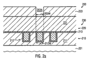
図2aは基板201を備えた半導体デバイス200の断面図を模式的に示しており、基板201の上方にはメタライゼーションシステム230が形成され得る。メタライゼーションシステム230は任意の数のメタライゼーション層を備えていてよく、ここでは便宜上、第1のメタライゼーション層220及び第2のメタライゼーション層210が図2aに示されている。例えば幾つかの例示的な実施形態では、メタライゼーションシステム230は洗練された半導体デバイスの相互接続構造を代表していてよく、その半導体デバイスにおいては、回路要素(図示せず)は概ね50nm以下の臨界寸法を有していてよい。半導体デバイス100を参照して前述したように、メタライゼーションシステム230の下方に位置していてよい適切な半導体材質の内部及び上方には、対応する回路要素が形成されていてよい。また、メタライゼーション層210,220は同様の構造を有していてよく、図1a及び1bを参照して説明したデバイス100の層110,120について論じられたとおりである。例えばメタライゼーション層210は、低k誘電体材質等のような誘電体材質211を備えていてよく、誘電体材質211内には、少なくとも図2aに示されるデバイス部分においては「狭ピッチ(narrow pitch)」の金属線を代表し得る金属線212が埋め込まれていてよい。即ち、金属線212は、メタライゼーション層210の臨界寸法を代表し得る幅212Wを有していてよく、洗練された応用においては、臨界寸法は概ね100nm以下である。しかし、他の例示的な実施形態においては、金属線212は、全体的な設計規則及び考慮中のメタライゼーションレベルに応じて、より大きな幅を有していてよいことが理解されるべきである。また、エッチング停止層213、例えばシリコン窒化物層、シリコンカーバイド、窒素豊富シリコンカーバイド層、又は他の適切な材質が、適切なエッチング停止能力を有するように、そして必要であれば前述したように銅閉じ込め特性に有効なように設けられていてよい。図示される製造段階においては、メタライゼーション層220はパターニングされていない誘電体材質221の形態で設けられてよく、誘電体材質221は、その内部に幅広の金属線を少なくとも密集した金属線212の上方に形成するために必要な任意の適切な組成を有していてよい。更に、図示される製造段階においては、例えばレジストマスクの形態にあるエッチングマスク203が誘電体材質221の上方に設けられてよく、エッチングマスク203は、誘電体材質221内に形成されることになるビア開口の目標横方向寸法に対応する横方向寸法203Wを有するマスク開口203Aを備えている。即ち、幅203Wは対応するビア開口の底でのその幅に実質的に一致していてよく、それにより、破線で示されるように、任意の隣接する金属線212に干渉することなしに、金属線212の1つへの確実な接続を可能にしている。例えば幅203Wは、金属線212の対応する幅212Wに実質的に等しいか又はそれよりも小さくてよい。
FIG. 2 a schematically shows a cross-sectional view of a
図2aに示される半導体デバイス200は、半導体デバイス100を参照して説明したようなプロセス技術に基いて形成することができる。従って幾つかの例示的な実施形態では、従来のプロセスとの高度な互換性が達成され得る。例えば、エッチングマスク203は十分に確立されたプロセス技術に基いて形成することができるが、ここでは、図1bに示される不規則性122Cのような任意の堆積関連の不規則性を抑えるためにしばしば用いられることがある横方向サイズが増大された付加的な層を必要とすることなしに、マスク開口203Aは幅212Wに対応するように設計されてよい。
The
図2bはエッチング環境204に曝露されるときの半導体デバイス200を模式的に示しており、エッチング環境204は、十分に確立されたエッチングレシピに基いて作り出されるエッチング環境を代表していてよい。従って、エッチングプロセス204の間、層221の材質が高度に異方性の様態で除去されてよく、それにより、マスク開口203Aの横方向サイズに実質的に対応する横方向サイズを有するビア開口221Vが得られる。幾つかの例示的な実施形態では、エッチングプロセス204は、ビア開口221Vの深さ221Dがビア開口221Vの最終的な深さ、即ち誘電体材質221の厚みの概ね3分の1又はそれよりも小さくなり得るように制御されてよい。エッチングプロセス204の対応する制御は、材質221に対する除去速度を決定すること及びエッチングプロセス204のプロセス時間を適切に調節することによって容易に達成することができる。
FIG. 2b schematically illustrates the
図2cは材質除去プロセス205Aの間における半導体デバイス200を模式的に示しており、材質除去プロセス205Aはエッチングマスク203の材質を除去するように設計される。例えば、プロセス205Aは酸素種を用いるプラズマ支援プロセスとして実行されてよい一方で、他の場合には、任意の他の適切なプラズマ支援エッチング環境が用いられてよく、そのエッチング環境においては、誘電体材質221のかなりの部分を除去することなしに有機材質を除去することができる。更に他の例示的な実施形態においては、プロセス205Aは、十分に確立された選択的エッチング薬品に基いて実行され得るウエット化学的レジスト除去プロセスを含んでいてよい。その結果、プロセス205Aの間、最初のエッチングマスク203は侵食され、それにより、幅203Eで示されるように開口203Aの横方向サイズを増大させることができる。増大された横方向幅203Eは、プロセス205Aのエッチング環境におけるエッチングマスク203の材質の除去速度を決定すること及びエッチング時間を制御することによって、効果的に調節され得ることが理解されるべきである。誘電体材質221に対するエッチングプロセス205Aの選択性に起因して、ビア開口221Vの最初の横方向幅は、少なくともその底では実質的に維持され得る。
FIG. 2c schematically illustrates the
図2dは更なるエッチングステップ204Bの間における半導体デバイス200を模式的に示しており、エッチングステップ204Bは、層221の材質がエッチングマスク203に対して選択的に除去され得るように、プロセス204A(図2b参照)と同じエッチングレシピに基いて行うことができる。幅203Eの増大に起因して、ビア開口221Vの幅もまたその上端で増大するであろう一方で、深さもまた221Eで示されるように増大するが、底部幅は最初の幅103W(図2c参照)に実質的に対応しているであろう。幾つかの例示的な実施形態では、エッチングプロセス204Bの異方性はプロセス204Aと比較してそれほど明白ではないであろうから、異なる横方向の幅203W及び203E(図2c参照)に起因する角又は段差の顕著な「丸まり(rounding)」が得られ、それにより、図2dに示されるように、多かれ少なかれ先細りの構造が得られる。
FIG. 2d schematically illustrates the
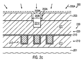
図2eは更なる例示的な実施形態に従う半導体デバイス200を模式的に示しており、その実施形態においては、必要な変化の程度(degree of graduation)及び先細りの程度に応じて図2c及び2dのプロセス205A、204Bを1回以上繰り返すことによって、更に明白な程度の先細りを達成することができる。例えば、図示されるように、デバイス200は更なるレジスト侵食プロセス205Bに曝されてよく、それによりマスク開口203Aの更に増大した横方向サイズ203Fを得ることができる。この目的のために、プロセス205A(図2c参照)に対して説明したのと同一の又は同等のプロセスレシピが用いられてよい。
FIG. 2e schematically illustrates a
図2fはビア221Vの深さを更に増大させるために更なるエッチングプロセス204Cに曝されるときの半導体デバイス200を模式的に示しており、図示される実施形態においては、ビア221Vはエッチング停止層213にまで下方向に拡張されてよい。しかし、全体的なプロセス戦略に応じてビア221Vの任意の他の深さが選択され得ることが理解されるべきである。例えば、誘電体材質221の上部内に溝が形成されることになる場合には、ビア開口221Vを形成するための最終的なエッチングステップが、対応する溝を得るための対応するエッチングステップと共通に実行されてよい。レジスト侵食/エッチングサイクルの所望のアンバー(amber)を形成し且つビア開口221Vの所望の深さを達成した後、エッチングマスク203を除去することによって更なる処理が継続されて良く、このことは十分に確立されたレシピによって達成することができ、その後、ビア開口221Vの上方に形成されることになる幅広の溝の横方向サイズを規定するために、更なるエッチングマスクが形成されてよい。この目的のために、場合によっては、対応するフィルム材質が表面形状を平坦化するように堆積させられてよく、そして平坦化された表面形状に基いて十分に確立されたリソグラフィ技術を用いて対応するエッチングマスクが形成されてよい。その後、例えば半導体デバイス100を参照して説明したように、ビア開口221V及び対応する幅広の溝は共通の堆積シーケンスにおいて充填されてよい。
FIG. 2f schematically illustrates the
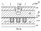
図2gは更なる例示的な実施形態に従う半導体デバイス200を模式的に示しており、その実施形態においては、スペーサ要素に基いてビア開口の明白な先細りを得ることができる。図示されるように、ビア開口221Vが、最初の幅221Jを有し且つ第1の深さ221Dを有するように誘電体材質221内に形成されてよく、第1の深さ221Dは、例えば、ビア開口221Vの最終的な深さの概ね40%〜60%を示してよい。また、図示される製造段階においては、スペーサ要素206Aがビア開口221Vの側壁上に形成されてよく、幾つかの例示的な実施形態では、スペーサ要素206Aは、誘電体材質221と同等のエッチング挙動を有する材質から構成されてよい。即ち、層221の材質を除去するように設計されたエッチングプロセスの間における除去速度は、スペーサ要素206Aの材質に対して、誘電体材質221と対比して概ねプラスマイナス10%の範囲内にあってよい。1つの例示的な実施形態では、スペーサ要素206Aは、誘電体材質221と実質的に同一な材質組成に基いて形成されてよい。このようにして、ビア開口221Vの更なるパターニングの間に、実質的に同一のエッチング挙動を達成することができる。また、図示される実施形態においては、必要であれば、全体的なプロセス要求に応じて、二酸化シリコン材質、シリコン窒化物材質等のようなエッチング停止ライナ206Bが、数nm乃至概ね10nm以上の厚みで設けられてよい。
FIG. 2g schematically shows a
図2gに示される半導体デバイス200は、以下のプロセスに基いて形成され得る。誘電体材質221を堆積させた後、レジストマスクのような適切なエッチングマスクが形成されてよく、エッチングマスクは、ビア開口221Vの最初の幅221Jに対応する横方向寸法を有する開口を備えていてよい。次いで、既に論じられたような十分に確立されたレシピに基いて異方性エッチングプロセスが実行されてよく、その結果、第1の深さ221Dまで延びるビア開口221Vが得られる。その後、レジストマスクは除去されてよく、そしてスペーサ層(図示せず)が場合によってはエッチング停止ライナ206Bとの組み合わせにおいて堆積させられてよく、このことは、十分に確立された堆積技術によって達成され得る。次いで、誘電体材質221と対比したスペーサ材質のエッチング挙動の類似性により、例えばビア開口221Vを形成するためにも用いられたであろうのと同様のエッチングレシピに基いて、スペーサ材質がエッチングされてよい。その結果、スペーサ層の材質が水平デバイス部分から及びビア開口221Vの中央から除去されてよく、ここでは、エッチング停止ライナ206Bが設けられている場合にはエッチング停止ライナ206Bで又はその内部でエッチングフロントの進行を確実に停止させることができる。この場合、特定の程度の「オーバエッチング(over etching)」が適用されてよく、その結果、ビア開口221Vの上部でのスペーサ要素206Aの明白な丸まり(rounding)が得られる。その後、幾つかの例示的な実施形態では、例えば適切な選択されたウエット化学的エッチングレシピ、プラズマ支援エッチングプロセス等によって、エッチング停止ライナ206Bの露出された部分が除去されてよい。他の例示的な実施形態においては、エッチング停止ライナ206Bが維持されると共に対応する溝エッチングマスクがライナ206B上に形成されてよい。
The
図2hは更に進んだ製造段階における半導体デバイス200を模式的に示している。図示されるように、エッチングマスク207が誘電体材質221の上方に形成されてよく、エッチングマスク207は、誘電体材質221の上部内に形成される溝221Tの位置及び横方向サイズを規定するために開口207Aを備えていてよい。例えば、溝221Tは、金属線212の幅212Wよりも大幅に大きいであろう幅221Wを有する幅広金属線を表してよい。幾つかの例示的な実施形態では、幅221Wは幅212Wの2倍又はそれよりも大きくてよく、それにより、前述したように増大された電流駆動能力を提供することができる。
FIG. 2h schematically shows the
エッチングマスク207は十分に確立されたプロセス戦略に基いて形成することができ、そのプロセスにおいては、必要であれば、適切なフィルム材質と溝221Tの横方向の位置及びサイズに従ってレジスト材質をパターニングするためのリソグラフィプロセスを実行することとによって、表面形状が平坦化されてよい。ビア開口221V(図2h参照)は必ずしも溝221Tの中央を中心としていなくてよく、従って、任意の適切な構造、即ちビア開口221Vと溝221Tの間での空間的関係が達成され得る。その後、例えば何らかの平坦化材質が設けられている場合にはその露出させられた部分を除去し、またエッチング停止ライナ206B(図2g)についてもその露出させられた部分をエッチングするために、半導体デバイス200はエッチングシーケンスに曝されてよい。その後、エッチングマスク207に基いて層221の材質を除去するように異方性エッチングプロセス204Dが実行されてよく、ここでは、ビア開口221Vはまた、誘電体材質221の下部内へ「移される(transferred)」。スペーサ要素206Aの存在により、ビア開口221Vの明白な先細りが達成され、その結果、ビア開口221Vの底部での減少させられた幅221Bを金属線212の幅212Wに適合させることができる。一方、ビア開口221Vは、顕著に増大された幅で溝221T内へと終端することができ、その増大された幅は幅221Jによって最初に規定されたものであってよく、ここでは、エッチングプロセス204Dの間に追加的な角の丸まり(corner rounding)が生じるので、ビア開口221Vの上部で最終的に得られる幅を更に増大し得ることが理解されるべきである。エッチングプロセス204Dの間、エッチング停止材質206Bは両側からアタックされ得るので、つまりスペーサ206Aを次第に除去すると共に層206Bの対向側で露出させられた材質221の部分を更に除去することによって材質が露出させられ得るので、エッチングプロセス204Dの間にエッチング停止ライナ206Bもまた除去されるであろうことが理解されるべきである。エッチングプロセス204Dの後、金属線212の表面部分を露出させるために、マスク207が除去されてよく、またエッチング停止213もビア開口221Vの範囲内で除去されてよい。
The
その結果、この場合にも、ビア開口221Vの明白な先細りを達成することができるので、伝導性バリア層を形成するための後続のプロセスシーケンスに対して大幅に強化された表面形状を提供することができ、また電気化学的堆積プロセスに基いて銅又は任意の他の高伝導性材質を充填することができる。
As a result, in this case as well, a clear taper of the via
図2iは更に進んだ製造段階における半導体デバイス200を模式的に示している。図示されるように、幅広の金属線222Lが先細りのビア222Vの上方に形成され、ビア222Vは、幅広の金属線222Lを下層のメタライゼーション層210の金属線212の1つに接続している。既に示したように、幅広の金属線222Lの幅222Wは幅212Wよりも著しく大きいであろうから、金属線222Lの高駆動電流能力を提供することができる。同様に、ビア222Vの幅222Bは金属線212の幅212Wに実質的に一致しているであろうから、増大された横方向サイズの追加的なコンタクト区域を必要とせずに、確実な電気的接続を可能にする。一方、ビア222Vの頂部での幅222Tは底部幅222Bよりも著しく大きいであろうから、前述したように、強化された表面状態を充填プロセスの間に提供することができる。幾つかの例示的な実施形態では、底部幅222Bは頂部幅222Tの概ね60%以下である。
FIG. 2 i schematically shows the
図2iに示される半導体デバイス200は、伝導性バリア材質222Aを形成するための十分に確立されたプロセス技術に基いて形成することができ、ここでは、対応するビア開口の明白な先細りによってもたらされる強化された表面形状もまた、全体的なプロセス均一性及び信頼性を高めることができる。その後、デバイス100を参照して既に説明したように、銅材質又は任意の他の高伝導性材質が電気化学的に堆積させられてよく、ここでは、底部幅222Bと比較して顕著に増大された横方向寸法222Wにもかかわらず、信頼性のある下から上への充填挙動(bottom to top fill behavior)を達成することができる。その後、例えばCMPによって任意の過剰な材質が除去されてよく、そして金属線222L及び誘電体材質221上にキャップ材質を形成することによって更なる処理が継続されてよい。続いて、任意の更なるメタライゼーション層が必要に応じて形成されてよい。
The
結果として、本開示は、例えば対応するマスク開口の異なる横方向サイズに基いて2つ以上のエッチングステップを形成するようにレジストマスクを断続的に侵食することでエッチングシーケンスを修正することによって、遷移ビアの明白な先細りが達成され得る技術及び半導体デバイスを提供する。他の場合には、エッチングプロセスはビア開口の「最大」横方向サイズで開始してよく、横方向サイズは、適切に寸法を決定されたスペーサ要素に基いて、更に進行したエッチングプロセスの間に減少させられてよい。 As a result, the present disclosure transitions by modifying the etching sequence, for example, by eroding the resist mask intermittently to form two or more etching steps based on different lateral sizes of the corresponding mask openings. Techniques and semiconductor devices are provided in which overt taper of the via can be achieved. In other cases, the etching process may begin with the “maximum” lateral size of the via opening, which is determined during the further etching process, based on appropriately dimensioned spacer elements. May be reduced.
本開示の更なる修正及び変更は、この明細書を考慮することによって当業者には明白になろう。従って、明細書は、例示的なものとしてのみ解釈されるべきであり、またここに開示される原理を実施する一般的な手法を当業者に教示することを目的としている。ここに示されまた説明される形態は目下のところ望ましい実施形態として解釈されるべきことが理解されるべきである。 Further modifications and variations of the present disclosure will become apparent to those skilled in the art from consideration of this specification. Accordingly, the specification is to be construed as illustrative only and is for the purpose of teaching those skilled in the art the general manner of carrying out the principles disclosed herein. It should be understood that the form shown and described herein is to be construed as the presently preferred embodiment.
Claims (21)
前記第1の横方向サイズを有する前記マスク開口に基き前記誘電体材質内で第1の深さまで延びるようにビア開口を形成することと、
前記マスク開口が第2の横方向サイズを有するように前記マスク開口を増大させることと、
前記第2の横方向サイズを有する前記マスク開口に基き第2の深さまで延びるように前記ビア開口を増大させることと、
前記誘電体材質内において前記ビア開口の上方に前記ビア開口に接続するように溝を形成することと、
前記ビア開口及び前記溝を金属含有材質で共通に充填することとを備えた方法であって、
前記ビア開口は前記第1のメタライゼーション層の下方に位置する第2のメタライゼーション層の金属領域まで延びる方法。 An etching mask comprising a mask opening having a first lateral size corresponding to a target lateral size at a bottom of a via to be formed in a dielectric material of a first metallization layer of a semiconductor device Forming above the dielectric material;
Forming a via opening to extend to a first depth within the dielectric material based on the mask opening having the first lateral size;
Increasing the mask opening such that the mask opening has a second lateral size;
Increasing the via opening to extend to a second depth based on the mask opening having the second lateral size;
Forming a groove to connect to the via opening above the via opening in the dielectric material;
Filling the via opening and the groove with a metal-containing material in common,
The via opening extends to a metal region of a second metallization layer located below the first metallization layer.
前記ビア開口の側壁上にスペーサ要素を形成することと、
前記第1のメタライゼーション層の下方に形成される第2のメタライゼーション層の金属領域まで延びるように前記ビア開口の深さを増大させることとを備えた方法。 Forming a via opening in the dielectric material of the first metallization layer of the semiconductor device extending to a first depth and having a first lateral size;
Forming a spacer element on a sidewall of the via opening;
Increasing the via opening depth to extend to a metal region of a second metallization layer formed below the first metallization layer.
前記第1のメタライゼーション層の下方に形成され、前記第1の幅よりも小さい第2の幅を有する第2の金属線を備えている第2のメタライゼーション層と、
前記第1の金属線から前記第2の金属線へ延びるビアとを備えた半導体デバイスであって、
前記ビアは前記第1の金属線での第1の横方向寸法と前記第2の金属線での第2の横方向寸法とを有しており、前記第2の横方向寸法は前記第1の横方向寸法の概ね60パーセント以下である半導体デバイス。 A first metallization layer formed above the substrate and comprising a metal line having a first width;
A second metallization layer comprising a second metal line formed below the first metallization layer and having a second width smaller than the first width;
A semiconductor device comprising a via extending from the first metal line to the second metal line,
The via has a first lateral dimension at the first metal line and a second lateral dimension at the second metal line, wherein the second lateral dimension is the first lateral dimension. A semiconductor device that is approximately 60 percent or less of the lateral dimension of
Applications Claiming Priority (5)
| Application Number | Priority Date | Filing Date | Title |
|---|---|---|---|
| DE102008063430.1A DE102008063430B4 (en) | 2008-12-31 | 2008-12-31 | Method for producing a metallization system of a semiconductor device with additionally tapered junction contacts |
| DE102008063430.1 | 2008-12-31 | ||
| US12/634,216 US8835303B2 (en) | 2008-12-31 | 2009-12-09 | Metallization system of a semiconductor device comprising extra-tapered transition vias |
| US12/634,216 | 2009-12-09 | ||
| PCT/EP2009/009308 WO2010076019A1 (en) | 2008-12-31 | 2009-12-29 | A metallization system of a semiconductor device comprising extra-tapered transition vias |
Publications (2)
| Publication Number | Publication Date |
|---|---|
| JP2012514319A true JP2012514319A (en) | 2012-06-21 |
| JP2012514319A5 JP2012514319A5 (en) | 2013-02-07 |
Family
ID=42234624
Family Applications (1)
| Application Number | Title | Priority Date | Filing Date |
|---|---|---|---|
| JP2011542726A Pending JP2012514319A (en) | 2008-12-31 | 2009-12-29 | Semiconductor device metallization system with specially tapered transition vias |
Country Status (6)
| Country | Link |
|---|---|
| US (1) | US8835303B2 (en) |
| JP (1) | JP2012514319A (en) |
| KR (1) | KR20130127013A (en) |
| CN (1) | CN102362343B (en) |
| DE (1) | DE102008063430B4 (en) |
| WO (1) | WO2010076019A1 (en) |
Families Citing this family (22)
| Publication number | Priority date | Publication date | Assignee | Title |
|---|---|---|---|---|
| FR2975826A1 (en) * | 2011-05-27 | 2012-11-30 | St Microelectronics Crolles 2 | Method for manufacturing integrated circuit, involves performing partial etching on layer through another layer until cavity crosses through layer, engraving partial layers in side walls of cavity, and completely removing former layer |
| JP2013021001A (en) * | 2011-07-07 | 2013-01-31 | Renesas Electronics Corp | Semiconductor device and semiconductor device manufacturing method |
| US8987916B2 (en) * | 2011-11-28 | 2015-03-24 | Freescale Semiconductor, Inc. | Methods and apparatus to improve reliability of isolated vias |
| JP5891846B2 (en) * | 2012-02-24 | 2016-03-23 | 富士通セミコンダクター株式会社 | Manufacturing method of semiconductor device |
| US8815752B2 (en) | 2012-11-28 | 2014-08-26 | Micron Technology, Inc. | Methods of forming features in semiconductor device structures |
| US9305886B2 (en) * | 2013-12-18 | 2016-04-05 | Globalfoundries Singapore Pte. Ltd. | Integrated circuits having crack-stop structures and methods for fabricating the same |
| US10163778B2 (en) | 2014-08-14 | 2018-12-25 | Taiwan Semiconductor Manufacturing Co., Ltd. | Structure and formation method of damascene structure |
| CN104505471B (en) * | 2014-12-22 | 2017-12-29 | 昆山工研院新型平板显示技术中心有限公司 | A kind of preparation method and mask plate of high aperture mask plate |
| KR20160120891A (en) | 2015-04-09 | 2016-10-19 | 삼성전자주식회사 | Semiconductor devices |
| US9536826B1 (en) * | 2015-06-15 | 2017-01-03 | Taiwan Semiconductor Manufacturing Co., Ltd. | Fin field effect transistor (finFET) device structure with interconnect structure |
| US9679850B2 (en) * | 2015-10-30 | 2017-06-13 | Taiwan Semiconductor Manufacturing Company Ltd. | Method of fabricating semiconductor structure |
| US9917027B2 (en) * | 2015-12-30 | 2018-03-13 | Globalfoundries Singapore Pte. Ltd. | Integrated circuits with aluminum via structures and methods for fabricating the same |
| CN107622992B (en) | 2016-07-14 | 2021-04-27 | 联华电子股份有限公司 | Semiconductor element and manufacturing method thereof |
| US10276485B2 (en) * | 2017-08-02 | 2019-04-30 | Taiwan Semiconductor Manufacturing Co., Ltd. | Method for forming a homogeneous bottom electrode via (BEVA) top surface for memory |
| US10998259B2 (en) * | 2017-08-31 | 2021-05-04 | Taiwan Semiconductor Manufacturing Company, Ltd. | Semiconductor device and method of manufacture |
| US10522394B2 (en) * | 2017-09-25 | 2019-12-31 | Marvell World Trade Ltd. | Method of creating aligned vias in ultra-high density integrated circuits |
| US10566411B2 (en) * | 2017-12-07 | 2020-02-18 | Globalfoundries Inc. | On-chip resistors with direct wiring connections |
| KR20200016472A (en) | 2018-08-07 | 2020-02-17 | 삼성전자주식회사 | Semiconductor device and method for fabricating the same |
| WO2020140202A1 (en) | 2019-01-02 | 2020-07-09 | Yangtze Memory Technologies Co., Ltd. | Method for forming dual damascene interconnect structure |
| CN112151497B (en) * | 2019-06-28 | 2023-08-22 | 台湾积体电路制造股份有限公司 | Semiconductor structure and method for forming semiconductor structure |
| US20210020455A1 (en) * | 2019-07-17 | 2021-01-21 | Nanya Technology Corporation | Conductive via structure |
| US11652049B2 (en) | 2021-03-10 | 2023-05-16 | Taiwan Semiconductor Manufacturing Co., Ltd. | Semiconductor device and method of forming thereof |
Citations (9)
| Publication number | Priority date | Publication date | Assignee | Title |
|---|---|---|---|---|
| US4902377A (en) * | 1989-05-23 | 1990-02-20 | Motorola, Inc. | Sloped contact etch process |
| JPH03257822A (en) * | 1990-03-07 | 1991-11-18 | Sanyo Electric Co Ltd | Manufacture of semiconductor device |
| JPH06260442A (en) * | 1992-11-27 | 1994-09-16 | Mitsubishi Electric Corp | Semiconductor device and manufacture thereof |
| JPH10163316A (en) * | 1996-12-04 | 1998-06-19 | Sony Corp | Formation of buried wiring in semiconductor device |
| JP2000260873A (en) * | 1999-01-08 | 2000-09-22 | Nec Corp | Forming method for contact or interconnection on semiconductor device |
| JP2001358213A (en) * | 2000-06-13 | 2001-12-26 | Nec Corp | Method for manufacturing semiconductor device having taper-like through hole |
| JP2003060035A (en) * | 2001-06-27 | 2003-02-28 | Hynix Semiconductor Inc | Method for forming dual damascene wiring |
| JP2006332503A (en) * | 2005-05-30 | 2006-12-07 | Fujitsu Ltd | Semiconductor device and method of manufacturing same |
| JP2007149773A (en) * | 2005-11-24 | 2007-06-14 | Mitsumi Electric Co Ltd | Method of manufacturing semiconductor device |
Family Cites Families (14)
| Publication number | Priority date | Publication date | Assignee | Title |
|---|---|---|---|---|
| US4472240A (en) * | 1981-08-21 | 1984-09-18 | Tokyo Shibaura Denki Kabushiki Kaisha | Method for manufacturing semiconductor device |
| US4698128A (en) * | 1986-11-17 | 1987-10-06 | Motorola, Inc. | Sloped contact etch process |
| JP3427534B2 (en) * | 1995-01-11 | 2003-07-22 | ソニー株式会社 | Forming connection holes |
| US6025259A (en) * | 1998-07-02 | 2000-02-15 | Advanced Micro Devices, Inc. | Dual damascene process using high selectivity boundary layers |
| US6239017B1 (en) * | 1998-09-18 | 2001-05-29 | Industrial Technology Research Institute | Dual damascene CMP process with BPSG reflowed contact hole |
| TW430943B (en) * | 1999-01-08 | 2001-04-21 | Nippon Electric Co | Method of forming contact or wiring in semiconductor device |
| TW424301B (en) * | 1999-10-02 | 2001-03-01 | Taiwan Semiconductor Mfg | Manufacturing method for dual damascene |
| US6440847B1 (en) * | 2001-04-30 | 2002-08-27 | Taiwan Semiconductor Manufacturing Company | Method for forming a via and interconnect in dual damascene |
| US6861347B2 (en) * | 2001-05-17 | 2005-03-01 | Samsung Electronics Co., Ltd. | Method for forming metal wiring layer of semiconductor device |
| US6605540B2 (en) * | 2001-07-09 | 2003-08-12 | Texas Instruments Incorporated | Process for forming a dual damascene structure |
| KR100454128B1 (en) * | 2002-04-02 | 2004-10-26 | 삼성전자주식회사 | Inter Metal Dielectric Pattern And Method Of Forming The Same |
| KR100529676B1 (en) * | 2003-12-31 | 2005-11-17 | 동부아남반도체 주식회사 | Method for fabricating dual damascene pattern |
| US8264086B2 (en) * | 2005-12-05 | 2012-09-11 | Taiwan Semiconductor Manufacturing Company, Ltd. | Via structure with improved reliability |
| DE102006025405B4 (en) * | 2006-05-31 | 2018-03-29 | Globalfoundries Inc. | Method for producing a metallization layer of a semiconductor device with different thickness metal lines |
-
2008
- 2008-12-31 DE DE102008063430.1A patent/DE102008063430B4/en active Active
-
2009
- 2009-12-09 US US12/634,216 patent/US8835303B2/en active Active
- 2009-12-29 WO PCT/EP2009/009308 patent/WO2010076019A1/en active Application Filing
- 2009-12-29 KR KR1020117016628A patent/KR20130127013A/en not_active Application Discontinuation
- 2009-12-29 CN CN200980157543.1A patent/CN102362343B/en active Active
- 2009-12-29 JP JP2011542726A patent/JP2012514319A/en active Pending
Patent Citations (9)
| Publication number | Priority date | Publication date | Assignee | Title |
|---|---|---|---|---|
| US4902377A (en) * | 1989-05-23 | 1990-02-20 | Motorola, Inc. | Sloped contact etch process |
| JPH03257822A (en) * | 1990-03-07 | 1991-11-18 | Sanyo Electric Co Ltd | Manufacture of semiconductor device |
| JPH06260442A (en) * | 1992-11-27 | 1994-09-16 | Mitsubishi Electric Corp | Semiconductor device and manufacture thereof |
| JPH10163316A (en) * | 1996-12-04 | 1998-06-19 | Sony Corp | Formation of buried wiring in semiconductor device |
| JP2000260873A (en) * | 1999-01-08 | 2000-09-22 | Nec Corp | Forming method for contact or interconnection on semiconductor device |
| JP2001358213A (en) * | 2000-06-13 | 2001-12-26 | Nec Corp | Method for manufacturing semiconductor device having taper-like through hole |
| JP2003060035A (en) * | 2001-06-27 | 2003-02-28 | Hynix Semiconductor Inc | Method for forming dual damascene wiring |
| JP2006332503A (en) * | 2005-05-30 | 2006-12-07 | Fujitsu Ltd | Semiconductor device and method of manufacturing same |
| JP2007149773A (en) * | 2005-11-24 | 2007-06-14 | Mitsumi Electric Co Ltd | Method of manufacturing semiconductor device |
Also Published As
| Publication number | Publication date |
|---|---|
| KR20130127013A (en) | 2013-11-22 |
| CN102362343A (en) | 2012-02-22 |
| DE102008063430B4 (en) | 2016-11-24 |
| WO2010076019A1 (en) | 2010-07-08 |
| US8835303B2 (en) | 2014-09-16 |
| US20100164121A1 (en) | 2010-07-01 |
| CN102362343B (en) | 2015-03-25 |
| DE102008063430A1 (en) | 2010-07-08 |
Similar Documents
| Publication | Publication Date | Title |
|---|---|---|
| JP2012514319A (en) | Semiconductor device metallization system with specially tapered transition vias | |
| US10643895B2 (en) | Self-aligned interconnects formed using subtractive techniques | |
| US8420533B2 (en) | Metallization system of a semiconductor device comprising rounded interconnects formed by hard mask rounding | |
| US8048796B2 (en) | Microstructure device including a metallization structure with self-aligned air gaps formed based on a sacrificial material | |
| US20070077761A1 (en) | Technique for forming a copper-based metallization layer including a conductive capping layer | |
| US7745327B2 (en) | Method of forming a copper-based metallization layer including a conductive cap layer by an advanced integration regime | |
| US8377820B2 (en) | Method of forming a metallization system of a semiconductor device by using a hard mask for defining the via size | |
| KR20210000732A (en) | Via prefilling of fully aligned vias | |
| KR20110003562A (en) | Method of reducing erosion of a metal cap layer during via patterning in semiconductor devices | |
| US20170256449A1 (en) | Methods of forming conductive structures with different material compositions in a metallization layer | |
| US8492269B2 (en) | Hybrid contact structure with low aspect ratio contacts in a semiconductor device | |
| KR20080033300A (en) | Dry etchback of interconnect contacts | |
| US20030181034A1 (en) | Methods for forming vias and trenches with controlled SiC etch rate and selectivity | |
| US8383510B2 (en) | Semiconductor device comprising metallization layers of reduced interlayer capacitance by reducing the amount of etch stop materials | |
| US8658494B2 (en) | Dual contact metallization including electroless plating in a semiconductor device | |
| US20100052175A1 (en) | Reducing leakage and dielectric breakdown in dielectric materials of metallization systems of semiconductor devices by forming recesses | |
| US20080206986A1 (en) | Method of forming a copper-based metallization layer including a conductive cap layer by an advanced integration regime | |
| US7592258B2 (en) | Metallization layer of a semiconductor device having differently thick metal lines and a method of forming the same | |
| US20090294921A1 (en) | Semiconductor device comprising metal lines with a selectively formed dielectric cap layer | |
| US20090108462A1 (en) | Dual integration scheme for low resistance metal layers | |
| KR100752174B1 (en) | Method for forming copper metallization layer in semiconductor device using two seed layers | |
| US20070178690A1 (en) | Semiconductor device comprising a metallization layer stack with a porous low-k material having an enhanced integrity | |
| CN113594133A (en) | Semiconductor structure and forming method thereof | |
| JP2005129937A (en) | Low k integrated circuit interconnection structure | |
| JP2007184347A (en) | Semiconductor device and manufacturing method thereof |
Legal Events
| Date | Code | Title | Description |
|---|---|---|---|
| A521 | Written amendment |
Free format text: JAPANESE INTERMEDIATE CODE: A523 Effective date: 20121212 |
|
| A621 | Written request for application examination |
Free format text: JAPANESE INTERMEDIATE CODE: A621 Effective date: 20121212 |
|
| A977 | Report on retrieval |
Free format text: JAPANESE INTERMEDIATE CODE: A971007 Effective date: 20140205 |
|
| A131 | Notification of reasons for refusal |
Free format text: JAPANESE INTERMEDIATE CODE: A131 Effective date: 20140212 |
|
| A521 | Written amendment |
Free format text: JAPANESE INTERMEDIATE CODE: A523 Effective date: 20140512 |
|
| A02 | Decision of refusal |
Free format text: JAPANESE INTERMEDIATE CODE: A02 Effective date: 20141104 |