JP2012504875A - Optoelectronic semiconductor device manufacturing method and optoelectronic semiconductor device - Google Patents
Optoelectronic semiconductor device manufacturing method and optoelectronic semiconductor device Download PDFInfo
- Publication number
- JP2012504875A JP2012504875A JP2011530360A JP2011530360A JP2012504875A JP 2012504875 A JP2012504875 A JP 2012504875A JP 2011530360 A JP2011530360 A JP 2011530360A JP 2011530360 A JP2011530360 A JP 2011530360A JP 2012504875 A JP2012504875 A JP 2012504875A
- Authority
- JP
- Japan
- Prior art keywords
- layer
- semiconductor
- growth substrate
- solder
- support
- Prior art date
- Legal status (The legal status is an assumption and is not a legal conclusion. Google has not performed a legal analysis and makes no representation as to the accuracy of the status listed.)
- Pending
Links
Images
Classifications
-
- H—ELECTRICITY
- H10—SEMICONDUCTOR DEVICES; ELECTRIC SOLID-STATE DEVICES NOT OTHERWISE PROVIDED FOR
- H10H—INORGANIC LIGHT-EMITTING SEMICONDUCTOR DEVICES HAVING POTENTIAL BARRIERS
- H10H20/00—Individual inorganic light-emitting semiconductor devices having potential barriers, e.g. light-emitting diodes [LED]
- H10H20/01—Manufacture or treatment
- H10H20/011—Manufacture or treatment of bodies, e.g. forming semiconductor layers
- H10H20/018—Bonding of wafers
-
- H—ELECTRICITY
- H10—SEMICONDUCTOR DEVICES; ELECTRIC SOLID-STATE DEVICES NOT OTHERWISE PROVIDED FOR
- H10H—INORGANIC LIGHT-EMITTING SEMICONDUCTOR DEVICES HAVING POTENTIAL BARRIERS
- H10H20/00—Individual inorganic light-emitting semiconductor devices having potential barriers, e.g. light-emitting diodes [LED]
- H10H20/80—Constructional details
- H10H20/81—Bodies
- H10H20/815—Bodies having stress relaxation structures, e.g. buffer layers
-
- H—ELECTRICITY
- H10—SEMICONDUCTOR DEVICES; ELECTRIC SOLID-STATE DEVICES NOT OTHERWISE PROVIDED FOR
- H10H—INORGANIC LIGHT-EMITTING SEMICONDUCTOR DEVICES HAVING POTENTIAL BARRIERS
- H10H20/00—Individual inorganic light-emitting semiconductor devices having potential barriers, e.g. light-emitting diodes [LED]
- H10H20/80—Constructional details
- H10H20/84—Coatings, e.g. passivation layers or antireflective coatings
- H10H20/841—Reflective coatings, e.g. dielectric Bragg reflectors
Landscapes
- Led Devices (AREA)
- Semiconductor Lasers (AREA)
- Led Device Packages (AREA)
Abstract
本発明は、オプトエレクトロニクス半導体素子の製造方法において、成長基板上にエピタキシャル層列を成長させるステップと、前記エピタキシャル層列の成長基板とは反対側表面にコンタクト層とバリア層を被着するステップと、前記エピタキシャル層列内に複数のトレンチを形成することによって前記エピタキシャル層列を個別の半導体に構造化するステップと、前記トレンチ内に露出する半導体の少なくとも側方縁部に誘電層)を被着するステップと、前記半導体間のトレンチでハンダ層の第1部分を半導体へ被着するステップと、ハンダ層の第2部分を支持体に被着するステップと、前記半導体を成長基板とは反対側にてハンダ層を用いて支持体に接続させるステップを有し、ハンダ層の第1部分と第2部分が相互に溶融され半導体間の複数のトレンチがハンダ層によって充填され、エピタキシャル成長基板が剥離される。 The present invention relates to a method of manufacturing an optoelectronic semiconductor device, the step of growing an epitaxial layer sequence on a growth substrate, and the step of depositing a contact layer and a barrier layer on the surface of the epitaxial layer sequence opposite to the growth substrate; Structuring the epitaxial layer sequence into individual semiconductors by forming a plurality of trenches in the epitaxial layer sequence, and depositing a dielectric layer on at least a lateral edge of the semiconductor exposed in the trench Applying a first portion of the solder layer to the semiconductor in a trench between the semiconductor, applying a second portion of the solder layer to the support, and providing the semiconductor on the opposite side of the growth substrate The solder layer is used to connect to the support, and the first portion and the second portion of the solder layer are melted together to form a semiconductor A plurality of trenches are filled by the solder layer, the epitaxial growth substrate is peeled off.
Description
本発明は、オプトエレクトロニクス半導体素子を製造するための方法並びにオプトエレクトロニクス半導体素子に関している。 The present invention relates to a method for manufacturing an optoelectronic semiconductor device and an optoelectronic semiconductor device.
本特許出願は、独国特許出願102008050573.0号に基づく優先権を主張するものであり、当該基礎出願の開示事項を本願発明に取り込むものである。 This patent application claims priority based on the German patent application 102008050573.0, and incorporates the disclosure of the basic application into the present invention.
国際公開第03/065420号パンフレットには、エピタキシャル層列が成長基板上でエピタキシャルに成長され、引き続きエピタキシャル層列が成長基板とは反対側でハンダ層を用いて支持体に接合され、その後で成長基板がエピタキシャル層列から分離される、オプトエレクトロニクス半導体素子の製造方法が開示されている。このように製造されたいわゆる薄膜半導体素子は、次のような利点を有している。すなわち、成長基板に課する結晶構造と格子定数に対する厳しい設定を充たす必要なしで、支持体に対する材料として、良好な熱特性と電気的特性を備えた低コストな材料が選択できる利点である。さらにこの方法は次のような利点も有している。すなわち、通常は高価な成長基板、例えばGaN基板若しくはサファイア基板を、窒化物化合物半導体の成長のために再利用することが可能なことである。 In WO 03/064420, an epitaxial layer sequence is grown epitaxially on a growth substrate, and the epitaxial layer sequence is subsequently bonded to a support using a solder layer on the opposite side of the growth substrate and then grown A method of manufacturing an optoelectronic semiconductor device is disclosed in which the substrate is separated from the epitaxial layer sequence. The so-called thin film semiconductor device manufactured in this way has the following advantages. That is, it is an advantage that a low-cost material having good thermal characteristics and electrical characteristics can be selected as a material for the support without having to satisfy strict settings for the crystal structure and lattice constant imposed on the growth substrate. Further, this method has the following advantages. In other words, a normally expensive growth substrate, such as a GaN substrate or a sapphire substrate, can be reused for the growth of nitride compound semiconductors.
独国特許出願公開第10 2005 029 246 A1明細書からは、半導体チップを支持体に接合するのに使用することのできる適切なハンダ層列が公知である。 From DE 10 2005 029 246 A1 a suitable solder layer sequence is known which can be used to bond a semiconductor chip to a support.
本発明の課題は、良好な光学的特性及び/又は機械的特性の点で秀でている、オプトエレクトロニクス半導体素子のより良好な製造方法の提供とそのような良好なオプトエレクトロニクス半導体素子を提供することである。 The object of the present invention is to provide a better manufacturing method of an optoelectronic semiconductor device which is excellent in terms of good optical properties and / or mechanical properties and to provide such a good optoelectronic semiconductor device. That is.
上記課題は請求項1の特徴部分に記載の本発明によるオプトエレクトロニクス半導体素子の製造方法並びに請求項10の特徴部分に記載の本発明によるオプトエレクトロニクス半導体素子によって解決される。本発明の有利な実施例及び改善例は、従属請求項に記載されている。
The object is solved by a method for producing an optoelectronic semiconductor device according to the invention as defined in the characterizing portion of
本発明によるオプトエレクトロニクス半導体素子の製造方法では、まずエピタキシャル層列が成長基板上でエピタキシャル成長される。 In the method of manufacturing an optoelectronic semiconductor device according to the present invention, an epitaxial layer sequence is first epitaxially grown on a growth substrate.
このエピタキシャル層列は有利には窒化物系化合物半導体に基づいている。この「窒化物系化合物半導体に基づく」とは、本願との関連では、半導体層列若しくはその少なくとも1つの層がIII族窒化物系化合物半導体材料、有利にはInxAlyGa1-x-yNを含んでいることを意味する。この場合、0≦x≦1、0≦y≦1、x+y≦1である。但しこれらの材料は必ずしも前記関係式で数字的に表される組成を正確に有するものではないことを述べておく。それどころかInxAlyGa1-x-yN材料の物理的特性を実質的に代えることのない1つ若しくはそれ以上のドーパントや付加的な成分も有し得る。しかしながら簡素化を図るために、前記関係式にはたとえそれらが僅かな量の別の物質によって部分的に置き換え可能であったとしても結晶格子の主要な構成成分(In,Al,Ga,N)しか含ませない。
This epitaxial layer sequence is preferably based on a nitride-based compound semiconductor. And the "nitride-based compound semiconductor-based", in the context of the present application, the semiconductor layer sequence or at least one layer III nitride compound semiconductor material, preferably In x Al y Ga 1-xy N Is included. In this case, 0 ≦ x ≦ 1, 0 ≦ y ≦ 1, and x + y ≦ 1. However, it should be noted that these materials do not necessarily have the exact composition expressed numerically in the above relational expression. Rather In x Al y Ga 1-xy
オプトエレクトロニクス半導体素子のエピタキシャル層列では例えば成長基板に向いた側に、1つ若しくは複数のn型ドーピング層を含んだn型領域が含まれる。それに対して成長基板とは反対側のエピタキシャル層列には、1つ若しくは複数のp型ドーピング層を含んだp型領域が含まれる。このn型領域とp型領域は、それぞれ1つまたはそれ以上のドーピングされていない層も含み得る。 An epitaxial layer sequence of an optoelectronic semiconductor element includes an n-type region including one or more n-type doping layers, for example on the side facing the growth substrate. On the other hand, the epitaxial layer sequence opposite to the growth substrate includes a p-type region including one or more p-type doping layers. Each of the n-type region and the p-type region may also include one or more undoped layers.
n型領域とp型領域の間には、有利には活性層が設けられる。この活性層とは、LED又は半導体レーザーのビーム放射層であり得る。この活性層は例えばpn接合部として、あるいはダブルへテロ構造として、あるいは単一量子井戸構造若しくは多重量子井戸構造として形成され得る。この場合の量子井戸構造には、電荷担体が閉じ込め(Confinement)によってそのエネルギー状態の量子化を被るような構造を含むが、量子化の次元の数に関する情報は何も含まれない。それによりここではとりわけ、量子井戸、量子細線、量子ドット、並びにこれらの構造のあらゆる組み合わせが含まれる。 An active layer is preferably provided between the n-type region and the p-type region. This active layer may be a beam emitting layer of an LED or a semiconductor laser. This active layer can be formed, for example, as a pn junction, as a double heterostructure, or as a single quantum well structure or a multiple quantum well structure. The quantum well structure in this case includes a structure in which the charge carrier undergoes quantization of its energy state by confinement, but does not include any information on the number of dimensions of quantization. Thereby, here, among others, quantum wells, quantum wires, quantum dots, and any combination of these structures are included.
例えば窒化物系化合物半導体材料からなるエピタキシャル層列の場合には、成長基板は、特にサファイア基板か又は代替的にGaN基板であり得る。 In the case of an epitaxial layer sequence made of, for example, a nitride-based compound semiconductor material, the growth substrate can in particular be a sapphire substrate or alternatively a GaN substrate.
成長基板上へのエピタキシャル層列の成長後は有利にはコンタクト層、特に反射性のコンタクト層がエピタキシャル層列へ被着される。このコンタクト層は半導体材料の電気的な接続のために用いられており、特に半導体材料を用いたオームコンタクトの形成に用いられる。コンタクト層は例えばAl,Ag,Au,Ptなどを含み得るか、又はそれらから形成される。また場合によってはこれらのコンタクト層はフォトリソグラフィ技術によって構造化されてもよい。 After growth of the epitaxial layer sequence on the growth substrate, a contact layer, in particular a reflective contact layer, is preferably applied to the epitaxial layer sequence. This contact layer is used for electrical connection of semiconductor materials, and is particularly used for forming ohmic contacts using semiconductor materials. The contact layer can include or be formed from, for example, Al, Ag, Au, Pt, and the like. In some cases, these contact layers may be structured by photolithography techniques.
有利には前記コンタクト層上にはバリア層が被着される。このバリア層は特に次のような機能、すなわち後から被着されるハンダ層の材料がコンタクト層内へ拡散するのを防止する機能を有している。 A barrier layer is preferably deposited on the contact layer. This barrier layer particularly has the following function, that is, the function of preventing the material of the solder layer deposited later from diffusing into the contact layer.
後続の方法ステップにおいては、エピタキシャル層列内にトレンチを形成することによってエピタキシャル層列を、個別の半導体に構造化する。このトレンチによれば、エピタキシャル層列が有利には完全に分離される。つまりこれらのトレンチは、エピタキシャル層列の上に被着されるコンタクト層とバリア層も含めて成長基板とは反対側のエピタキシャル層列表面から成長基板の所まで延在している。 In subsequent method steps, the epitaxial layer sequence is structured into individual semiconductors by forming trenches in the epitaxial layer sequence. With this trench, the epitaxial layer sequence is advantageously completely separated. That is, these trenches extend from the surface of the epitaxial layer sequence opposite to the growth substrate, including the contact layer and barrier layer deposited on the epitaxial layer sequence, to the growth substrate.
前記トレンチは例えばエッチングプロセスを用いて形成可能である。 The trench can be formed using, for example, an etching process.
トレンチによって分離された半導体は、それぞれ側方縁部を有しており、これらの側方縁部がトレンチと接している。さらなる方法ステップにおいては、誘電層が少なくともトレンチ内へ露出した半導体側方縁部に被着される。誘電層は特にトレンチ内で露出した成長基板も覆う。たとえば誘電層はまず成長基板からの接合部と半導体上にフルフラットに被着され、それによって誘電層が半導体とその上に被着されるコンタクト層及びバリア層と共に覆い、さらに半導体の側縁部と、トレンチ内に露出した成長基板を覆う。半導体との電気的な接続を可能にするために、誘電層は、有利には、事前に被着されるバリア層内に開口部が形成されるように構造化される。 Each of the semiconductors separated by the trench has side edges, and these side edges are in contact with the trench. In a further method step, a dielectric layer is deposited at least on the semiconductor lateral edge exposed into the trench. The dielectric layer also covers the growth substrate exposed in particular in the trench. For example, the dielectric layer is first deposited flat on the junction from the growth substrate and the semiconductor, thereby covering the dielectric layer together with the semiconductor and the contact and barrier layers deposited thereon, and the side edges of the semiconductor. And the growth substrate exposed in the trench. In order to allow electrical connection with the semiconductor, the dielectric layer is advantageously structured such that openings are formed in the pre-deposited barrier layer.
前記誘電層は有利には窒化珪素層、例えば非化学量論的組成物、SiNx、又は二酸化珪素、例えばSiO2またはSiO2:P2O5などである。 The dielectric layer is preferably a silicon nitride layer, such as a non-stoichiometric composition, SiN x , or silicon dioxide, such as SiO 2 or SiO 2 : P 2 O 5 .
有利な実施例によれば、誘電層の被着と場合によっては誘電層の構造化の後で接着層及び/又は湿潤層が当該誘電層の上に設けられてもよい。この接着層及び/又は湿潤層は、誘電層に続くハンダ層の固着及び/又は濡れを向上させる機能を有している。前記接着層及び/又は湿潤層は例えばTiを含むか若しくはTiから形成され得る。 According to an advantageous embodiment, an adhesion layer and / or a wetting layer may be provided on the dielectric layer after the deposition of the dielectric layer and possibly the structuring of the dielectric layer. This adhesive layer and / or wetting layer has a function of improving the adhesion and / or wetting of the solder layer following the dielectric layer. The adhesive layer and / or the wetting layer may contain Ti or be made of Ti, for example.
それに続いてハンダ層の第1の部分が半導体上に被着され、トレンチ内では半導体の間に被着される。ハンダ層の第1の部分は、有利にはフルフラットで成長基板からの接合部と半導体と既に被着されている層上に被着される。このハンダ層の第1の部分は、半導体と、当該半導体の側縁部を越えて、半導体間のトレンチ内で、事前に被着された層を越えて延在している。 Subsequently, a first part of the solder layer is deposited on the semiconductor and in the trench between the semiconductors. The first part of the solder layer is preferably deposited on a layer that has already been deposited flat and flat with the junction from the growth substrate and the semiconductor. The first portion of the solder layer extends beyond the pre-deposited layer in the trench between the semiconductor and beyond the semiconductor and the side edges of the semiconductor.
ハンダ層の第1の部分は必ずしも個別化された層である必要はなく、それは複数のハンダ構成要素から成る層列であってもよい。例えばハンダ層は、そのもとで配置される接着層及び/又は湿潤層として、Ti層やAu層を含んでいてもよい。Sn層はハンダの第1の構成要素を表し、これは半導体を後で支持体に接着させるものである。それに続くTi層はバリア層を形成し、Au層は酸化保護膜として用いられる。このAuからなる酸化保護膜とSn層との間に配置されるTiからなるバリア層は、Snが後続のAu層内へ拡散することを防いでいる。 The first part of the solder layer need not necessarily be an individualized layer, it may be a layer sequence consisting of a plurality of solder components. For example, the solder layer may include a Ti layer or an Au layer as an adhesive layer and / or a wet layer disposed under the solder layer. The Sn layer represents the first component of the solder, which later bonds the semiconductor to the support. The subsequent Ti layer forms a barrier layer, and the Au layer is used as an oxidation protection film. The barrier layer made of Ti disposed between the oxidation protection film made of Au and the Sn layer prevents Sn from diffusing into the subsequent Au layer.
ハンダ層の第2の部分は、支持体に被着される。これは後で半導体と接着されてもよい。例えば前記支持体はゲルマニウム支持体であってもよい。半導体層の第2の部分は、例えばAuを有していてもよい。支持体と、ハンダ層の第2の部分との間には、1つ又は複数の介在層が設けられてもよい。 The second part of the solder layer is applied to the support. This may later be bonded to the semiconductor. For example, the support may be a germanium support. The second portion of the semiconductor layer may include Au, for example. One or more intervening layers may be provided between the support and the second portion of the solder layer.
特に支持体にはコンタクト層が被着可能である。このコンタクト層は例えばゲルマニウム支持体の半導体材料を後続の金属化層に接続させる。コンタクト層上には半導体上のように接着層及び/又は湿潤層が設けられていてもよい。例えばそれらはPt層やSn層からなる層列であってもよい。 In particular, a contact layer can be applied to the support. This contact layer, for example, connects the semiconductor material of the germanium support to the subsequent metallization layer. An adhesive layer and / or a wet layer may be provided on the contact layer as on a semiconductor. For example, they may be a layer sequence composed of a Pt layer or a Sn layer.
引き続き半導体は、成長基板とは反対側においてハンダ層を用いて支持体と接合される。 The semiconductor is subsequently bonded to the support using a solder layer on the side opposite the growth substrate.
ハンダ過程においては、成長基板からなる接合部と半導体上に被着されているハンダ層の第1部分と、支持体に被着されているハンダ層の第2部分が相互に溶融される。例えばハンダ層の第1部分がSnを含み、ハンダ層の第2部分はAuを含んでいてもよい。この場合はハンダ層の第1部分とハンダ層の第2部分が、ハンダ過程の間に、溶融されAuSn合金となる。 In the soldering process, the bonding portion made of the growth substrate, the first portion of the solder layer deposited on the semiconductor, and the second portion of the solder layer deposited on the support are melted together. For example, the first part of the solder layer may contain Sn and the second part of the solder layer may contain Au. In this case, the first part of the solder layer and the second part of the solder layer are melted into an AuSn alloy during the soldering process.
前記ハンダ過程においては、半導体間のトレンチがハンダ層によって充填される。ハンダ層の第1部分とハンダ層の第2部分の分量は、次のように設定される。すなわち当該のハンダ過程において、十分なハンダ材料が形成され、かつ半導体の間のトレンチが完全に充填され得るように設定される。そしてハンダ過程の後では、複数の半導体が有利には成長基板とは対向する側において支持体と接合される。半導体の間に存在する元の複数のトレンチがハンダ層によって完全に充填されることによって、そのように形成された接合部は、半導体間で不要な中空空間を何も持たないように形成される。 In the soldering process, the trench between the semiconductors is filled with a solder layer. The amounts of the first part of the solder layer and the second part of the solder layer are set as follows. That is, the soldering process is set so that a sufficient solder material is formed and the trench between the semiconductors can be completely filled. After the soldering process, the plurality of semiconductors are advantageously bonded to the support on the side facing the growth substrate. The original plurality of trenches existing between the semiconductors are completely filled with the solder layer, so that the junctions so formed are formed so as to have no unnecessary hollow spaces between the semiconductors. .
さらなる後続の方法ステップでは、成長基板が半導体から剥離される。この成長基板の剥離は、当該成長基板がサファイア基板のケースでよく用いられる、レーザーリフトオフ技法を用いて行われる。このレーザーリフトオフ技法のもとでは、半導体材料が基板を貫通するレーザービームを当てられる。その場合半導体層内におけるレーザービームの吸収は、基板内においてよりも多くなる。このレーザービームは、半導体材料内への高い吸収に基づいて境界面近傍で半導体層内へ吸収され、そこで材料の分解が引き起こされる。この材料分解によって半導体は成長基板から分離される。 In a further subsequent method step, the growth substrate is stripped from the semiconductor. The growth substrate is peeled off by using a laser lift-off technique, which is often used in the case of a sapphire substrate. Under this laser lift-off technique, a semiconductor material is irradiated with a laser beam that penetrates the substrate. In that case, the absorption of the laser beam in the semiconductor layer is greater than in the substrate. This laser beam is absorbed into the semiconductor layer in the vicinity of the interface due to high absorption into the semiconductor material, where it causes decomposition of the material. The semiconductor is separated from the growth substrate by this material decomposition.
支持体と半導体からなる接合部は、成長基板の剥離の際に、半導体間のトレンチを充填しているハンダ層によって安定化される。特に、少なくとも半導体の側縁部に被着された誘電層が、成長基板の剥離過程においてハンダ層によって安定化され保護される。 The joint made of the support and the semiconductor is stabilized by the solder layer filling the trench between the semiconductors when the growth substrate is peeled off. In particular, at least the dielectric layer deposited on the side edge of the semiconductor is stabilized and protected by the solder layer during the growth substrate peeling process.
本発明による方法の有利な構成例によれば、誘電層の被着の後、及び特に接着層及び/又は湿潤層及び後続のハンダ層の被着の前に、ミラー層が当該誘電層に被着される。このミラー層は特に金属又は金属化結合部を有し得る。例えばこのミラー層は、例えばAg,Pt,Al,Rhを含み得るか又はそれらから形成され得る。ミラー層は、事前に被着された誘電層のように少なくとも半導体の側縁部を越えて延在する。誘電層によってミラー層は半導体側縁部から絶縁され、そのようにして半導体のp型領域とn型領域の間で短絡が回避される。誘電層上のミラー層は、完成されたオプトエレクトロニクス半導体素子において次のような利点をもたらす。すなわち、ビームを放射する活性層から半導体側縁部方向へ放射される電磁ビームが戻されるように反射され、場合によっては1つ若しくは複数のさらなる反射の後で半導体においてビーム出射側から出力結合される。このようにしてビーム出射側からの電磁ビームの出力結合が向上する。 According to an advantageous embodiment of the method according to the invention, the mirror layer is applied to the dielectric layer after the deposition of the dielectric layer and in particular before the deposition of the adhesive layer and / or the wetting layer and the subsequent solder layer. Worn. This mirror layer may in particular have a metal or metallized joint. For example, the mirror layer can comprise or be formed from, for example, Ag, Pt, Al, Rh. The mirror layer extends at least beyond the side edges of the semiconductor, like a pre-deposited dielectric layer. The mirror layer is insulated from the semiconductor side edge by the dielectric layer, thus avoiding a short circuit between the p-type region and the n-type region of the semiconductor. The mirror layer on the dielectric layer provides the following advantages in the finished optoelectronic semiconductor device. That is, an electromagnetic beam radiated from the active layer emitting the beam toward the semiconductor side edge is reflected back, and in some cases after one or more further reflections, the semiconductor is outcoupled from the beam exit side. The In this way, the output coupling of the electromagnetic beam from the beam emission side is improved.
このようなミラー層による半導体側縁部領域におけるビーム出力結合の向上は、エッチングプロセスによって形成された半導体側縁部が傾斜している場合、つまり元の成長基板に対して直角ではなくて斜めに傾むくようにエッチングされている場合には特に効果的となる。 The improvement of beam output coupling in the semiconductor side edge region by such a mirror layer is achieved when the semiconductor side edge formed by the etching process is inclined, that is, not at right angles to the original growth substrate. This is particularly effective when etching is performed so as to be inclined.
ミラー層の被着の後では、有利には、例えば接着層及び/又は湿潤層並びに後続のハンダ層が被着される前に、保護層を当該ミラー層に被着してもよい。この保護層は、後に続くその他の層、例えばハンダ層との不都合な相互作用からミラー層を保護するためのものである。この保護層は、特に窒化珪素若しくは二酸化珪素からなる誘電層であってもよい。例えば前記保護層は、事前に被着された誘電層(この誘電層の上にミラー層が配置されている)と同じ材料から形成されていてもよい。しかしながら前記保護層は必ずしも電気的な絶縁性を備えている必要はない。そのため前記保護層は、例えば金属であってもよいし、例えばTiW(N,Ti,Niなどを有し得る)のような金属化合物であってもよい。 After application of the mirror layer, a protective layer may advantageously be applied to the mirror layer, for example before the adhesive layer and / or the wetting layer and the subsequent solder layer are applied. This protective layer is intended to protect the mirror layer from adverse interactions with other subsequent layers, such as solder layers. This protective layer may in particular be a dielectric layer made of silicon nitride or silicon dioxide. For example, the protective layer may be made of the same material as a pre-deposited dielectric layer (a mirror layer is disposed on the dielectric layer). However, the protective layer is not necessarily provided with electrical insulation. Therefore, the protective layer may be a metal, for example, or a metal compound such as TiW (which may have N, Ti, Ni, etc.).
当該方法の有利な実施例によれば、ハンダ層は、成長基板の剥離後に、半導体の間のトレンチから除去される。この半導体の間のトレンチからのハンダ層の除去は、特にエッチングプロセスを用いて行われてもよい。このエッチングは、元の成長基板の支持体に対向している側から行われる。 According to an advantageous embodiment of the method, the solder layer is removed from the trench between the semiconductors after the growth substrate has been stripped. This removal of the solder layer from the trenches between the semiconductors may be performed in particular using an etching process. This etching is performed from the side facing the support of the original growth substrate.
別の有利な実施例によれば、ハンダ層は、成長基板の剥離後も半導体チップ間のトレンチ内に残される。つまりトレンチから除去されない。そのようなケースでは、半導体チップはその上に被着される層と共に、特に側縁部においてハンダ層によって保護され安定化する。さらにトレンチがハンダ層で充填されることによってさらなるプロセスステップ(例えばフォトリソグラフィ技法における塗布プロセスなど)が容易となる。 According to another advantageous embodiment, the solder layer is left in the trench between the semiconductor chips after the growth substrate has been stripped. That is, it is not removed from the trench. In such a case, the semiconductor chip is protected and stabilized by a solder layer, particularly at the side edges, along with the layer deposited thereon. Furthermore, the trench is filled with a solder layer, which facilitates further process steps (such as a coating process in photolithography techniques).
個々の半導体の間のトレンチでは、支持体と被着された半導体からなる接合部が引き続き個別の半導体素子のために分断される。このようにして、1つ若しくはそれ以上の半導体を含んでいる、複数の半導体素子が形成される。ハンダ層が事前にトレンチから除去されないケースでは、ハンダ層がエピタキシャル層列を有利には半導体チップ取付けの際の機械的な破損から保護する。 In the trenches between the individual semiconductors, the support and the bonded semiconductor junction are subsequently divided for the individual semiconductor elements. In this way, a plurality of semiconductor elements including one or more semiconductors are formed. In the case where the solder layer is not previously removed from the trench, the solder layer advantageously protects the epitaxial layer sequence from mechanical damage during semiconductor chip attachment.
前述したような方法を用いることによって、ハンダ層を用いて支持体の主要平面と接合されている少なくとも1つの半導体を備えたオプトエレクトロニクス半導体素子が製造され得る。ここでは、支持体の主要平面に対して斜め方向若しくは直角方向に延在する半導体側縁部が誘電層を備えており、さらにそれらの誘電層上にはミラー層が被着されている。このミラー層は次のような利点を有する。すなわち、側縁部方向に放射される電磁ビームが戻るように反射され、有利にはビーム出射側において、半導体から有利な出力結合が生じるようになる。これにより、不都合な横方向への放射は、このようにして強化された垂直方向への放射のために低減される。 By using the method as described above, an optoelectronic semiconductor device comprising at least one semiconductor bonded to the main plane of the support using a solder layer can be produced. Here, the semiconductor side edge extending in an oblique direction or a right angle direction with respect to the main plane of the support body is provided with a dielectric layer, and a mirror layer is deposited on these dielectric layers. This mirror layer has the following advantages. That is, the electromagnetic beam radiated in the direction of the side edge is reflected back, and advantageous output coupling from the semiconductor occurs, preferably on the beam exit side. Thereby, inconvenient lateral radiation is reduced due to thus enhanced vertical radiation.
オプトエレクトロニクス半導体素子、特に半導体と該半導体に被着される層のさらに別の有利な実施例は、本発明による方法に関連して説明してきた前述の有利な実施例と同じように得ることができる。 Further advantageous embodiments of the optoelectronic semiconductor element, in particular the semiconductor and the layers deposited on the semiconductor, can be obtained in the same way as the previously described advantageous embodiments described in connection with the method according to the invention. it can.
このオプトエレクトロニクス半導体素子は、特に成長基板から開放される。このオプトエレクトロニクス半導体素子は有利には、エピタキシャル層列が、成長基板とは同一でない支持体と接合されているいわゆる薄膜半導体素子である。 This optoelectronic semiconductor element is in particular free from the growth substrate. This optoelectronic semiconductor element is preferably a so-called thin-film semiconductor element in which the epitaxial layer sequence is bonded to a support that is not identical to the growth substrate.
特に支持体に対向しているオプトエレクトロニクス半導体素子の主要面がエピタキシャル層列のn型領域側で、ビーム出力結合面として用いられ得る。良好なビーム出力結合を得るために、支持体に対向している半導体表面が所望のように構造化されるかないしは形成される。 In particular, the main surface of the optoelectronic semiconductor element facing the support can be used as the beam output coupling surface on the n-type region side of the epitaxial layer sequence. In order to obtain good beam output coupling, the semiconductor surface opposite the support is structured or formed as desired.
以下の明細書では、本発明によるオプトエレクトロニクス半導体素子の製造方法並びにオプトエレクトロニクス半導体素子を、図1〜図12に描写された実施例に基づいて詳細に説明する。 In the following specification, a method of manufacturing an optoelectronic semiconductor device and an optoelectronic semiconductor device according to the present invention will be described in detail based on the embodiments depicted in FIGS.
前記図面中、同じ構成要素ないし同じ機能の構成要素には、同じ符号が付されている。なおこれらの図面中に描写されている構成要素並びにそれらの構成要素相互間のサイズ比は必ずしも縮尺どおりではないことを述べておく。 In the drawings, the same components or components having the same functions are denoted by the same reference numerals. It should be noted that the components depicted in these drawings and the size ratios between those components are not necessarily to scale.
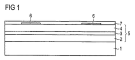
図1に示されている、本発明によるオプトエレクトロニクス半導体素子の製造方法の第1実施例の介在ステップにおいては、エピタキシャル層列5が成長基板1上でエピタキシャルに成長される。
In the intervening step of the first embodiment of the method for manufacturing an optoelectronic semiconductor device according to the invention shown in FIG. 1, an
これらのエピタキシャル層列5は、例えば窒化物化合物半導体に基づく半導体層列であってもよい。前記エピタキシャル層列5は、成長基板1の側にn型領域2を有し、成長基板1とは反対側にp型領域4を有している。前記n型領域2は、1つまたは複数のn型ドープされた層を含み、前記p型領域4は、1つまたは複数のp型ドープされた層を含んでいる。n型領域2とp型領域4の間には、活性層3、特に電磁ビームを放射する活性層3が含まれている。エピタキシャル層列5は、n型領域2と、活性層3と、p型領域4においてそれぞれ1つ若しくは複数のドープされていない層を含んでいてもよい。
These
前記成長基板1は、例えばサファイア又はGaNからなるウエハであってもよい。
The
エピタキシャル層列5の上にはコンタクト層6が被着されている。これらのコンタクト層6は、後の段階で、個々の半導体毎に電気的なコンタクトが形成されるように既に構造化されている。前記コンタクト層6は有利には反射型乃至ミラー型のコンタクト層であってもよい。このミラー型コンタクト層6は、例えばAl,Ag,Auを含むかそれらから形成されていてもよい。金属性のコンタクト層6は、p型領域4の半導体材料への電気的な接続部を形成し、有利にはコンタクト層の方向に放射されたビームをビーム出射側の方向に反射すべく、活性層3から放射されたビームを反射する。この場合のビーム出射側とは、以下の明細書でも説明するように、完成したオプトエレクトロニクス半導体素子において、もとの成長基板1の側に設けられている。
A
前記コンタクト層6の上方にはバリア層7が被着される。このバリア層7は、引き続き被着される層、特にハンダ層の構成要素の拡散成分からコンタクト層6を保護するための拡散ストッパーとして用いられている。このバリア層7としては例えばTiW(n型層)が適している。
A
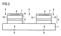
図2に示されている当該方法の介在ステップにおいては、エピタキシャル層列5が複数の個別の半導体8に構造化されている。その際には、複数のトレンチ9がエピタキシャル層列5内に形成される。これらのトレンチ9は、成長基板1の上に被着されるコンタクト層6及びバリア層7も含めて成長基板1とは反対側のエピタキシャル層列5の側から、成長基板1の所まで延在している。これらのトレンチ9は、例えばエッチング技法によって形成されてもよい。
In the intervening step of the method shown in FIG. 2, the
前記トレンチ9内では半導体8の側方縁部10が露出している。これらの側方縁部10は、必ずしも図2に示されているように、成長基板1に対して垂直方向に延在している必要はなく、例えば成長基板1に対して傾斜した方向に延在していてもよい。
In the
図3に示されている当該方法の介在ステップにおいては、前記半導体8の上方に誘電層11が被着される。この誘電層11は、例えば半導体8の側方縁部10を越えて延在し、後から被着されるさらなる層に対する電気的な絶縁を実現している。これらの誘電層11は次のように構造化されている。すなわち、成長基板1とは反対側の半導体8表面の少なくとも一部が当該誘電層11から開放され、それによって、コンタクト層6とバリア層7を備えた当該半導体8とさらなる導電層との電気的な接続が可能となるように構造化されている。図3に示されているように、誘電層11は半導体8の縁部領域から半導体8の側方縁部10を越えて延在し、さらにこれらの半導体8の間のトレンチ9領域においては成長基板1も覆っている。誘電層11は例えば非化学量論的な組成のSiNxなどの窒化珪素系の層であってもよいし、SiO2、SiO2:P2O2などの二酸化珪素系の層であってもよい。
In the intervening step of the method shown in FIG. 3, a
前記誘電層11の上には接着層及び/又は湿潤層として用いられる層12と、ハンダ層の第1部分13aが被着される。この接着層及び/又は湿潤層12とハンダ層はそれぞれ1つ若しくは複数の部分層から形成されていてもよい。前記接着層及び/又は湿潤層12は、例えばTiを含むか又はTiから形成されていてもよい。
On the
前記ハンダ層の第1部分13aは、有利にはSn,Ti,Auの順番で3つの部分層を含んでいる。但しこれらの3つの部分層は、見易くする理由から図3では個別に描写していない。前記接着層及び/又は湿潤層12に続くSn部分層は、ハンダ層の第1の構成要素としてSnを含んでいる。この第1の構成要素は、その後の時点でハンダ層の第1部分13aと第2部分13bの溶融の際に生じる。Snからなる部分層は、有利にはTiからなる拡散ストッパーとAuからなる酸化保護膜を備えている。Auからなる酸化保護膜は、Sn層を酸化から保護している。この場合Sn層とAu層の間に設けられるTi層が、Au層内へのSnの拡散を阻止する。
The
前記接着層及び/又は湿潤層12並びにハンダ層の第1部分13aは、有利には成長基板1と半導体8と事前に被着された層からなる接合部全体の上方に配設されている。つまり前記接着層及び/又は湿潤層12とハンダ層第1部分13aは、誘電層11から開放されているバリア層7の領域と、半導体の側方縁部10上方の誘電層11と、前記半導体の間のトレンチ9領域の誘電層11を覆っている。
The adhesive layer and / or the
ハンダ層の第2部分13bは、支持体14に設けられており、この支持体14は、成長基板1とは反対側の半導体に接続されるべきものである。
The
支持体14に設けられる半導体層の第2部分13bは、例えばAu層であってもよい。後の時点のハンダ過程において、半導体8の上方のハンダ層の第1部分13aと、支持体14下方のハンダ層の第2部分13bは相互に溶融され、金属性合金からなるハンダ層となる。例えばハンダ層の第1部分13aは、専らSnを含み、ハンダ層の第2部分13bはAuを含んでいてもよい。その場合にはハンダ層のこれらの2つの成分がハンダ過程において溶融されてAuSn合金となる。
The
例えばゲルマニウム支持体であり得る支持体14と、ハンダ層の第2の部分13bとの間には、有利にはさらなる層15,16,17が設けられていてもよい。支持体14は、有利には、金属若しくは金属性合金からなるコンタクト層15を備えていてもよく、この層15は支持体14との電気的なコンタクトを形成する。さらにこのコンタクト層15には、接着層16及び/又は湿潤層17が続いて設けられてもよい。前記接着層16は例えばTiを含み、前記湿潤層17は例えばPtを含んでいてもよい。
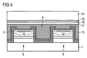
図4には、一方の側では支持体14から半導体8までの接合部が示され他方の側では成長基板1から半導体8までの接合部が示されている。ハンダ層の第1部分13aとハンダ層の第2部分13bは、ここでは溶融されて1つのハンダ層13となっている。
FIG. 4 shows the junction from the
このハンダ層13は、特にAuSnを含み得る。この接合部は、場合によっては、ハンダ系の層内に挿入される介在層、例えばTi層のようなさらなる構成要素を含んでいてもよい。
This
ハンダ過程においては、半導体の間にあるトレンチ9が有利にはハンダ層13によって完全に充たされる。事前に被着されるハンダ層の層厚さは、次のように選定される。すなわち、半導体8の間のトレンチ9を完全に充たすことのできる十分な厚みのハンダ層13が形成されるように選定される。半導体8の間のトレンチ9の充填によって、安定した接合部が支持体14と半導体8との間に形成され、この形成は後に続く半導体8からの成長基板1の剥離のために有利となる。さらに支持体14と半導体8との間に十分な分量で流入するハンダ13は、場合によって存在する、継ぎ目領域表面の凹凸を調整できる利点をもたらす。このハンダ層13によって特に半導体8の側方縁部10上方の誘電層11も安定化される。
In the soldering process, the
図5に示されている本発明による方法の介在ステップでは、成長基板1が半導体8から剥離される。特にサファイアからなる成長基板のケースでは、この剥離ステップがレーザーリフトオフ技法を用いて行うことが可能である。このレーザーリフトオフ技法自体は、冒頭において援用した国際公開第03/065420号パンフレットからも公知であるので、ここでの詳細な説明は省く。GaNからなる成長基板のケースでは、成長基板の剥離は例えば水素イオンのイオン打ち込みとそれに続く温度処理によって行われる。
In the intervening step of the method according to the invention shown in FIG. 5, the
またハンダ層13は、図6に示されているように、半導体8の間のトレンチ9からの成長基板の剥離後に除去されてもよい。このハンダ層13の除去は、例えばエッチングプロセスを用いて行われてもよい。また代替的に、ハンダ層13を半導体の間のトレンチ9から除去しないことも可能である。そのようなケースでは、残留するハンダ層13が有利には安定化層と保護層として機能する。
Further, the
もとの成長基板に向いた側の半導体8表面18は(この表面は完成後のオプトエレクトロニクス半導体素子においてビーム出力結合面として用いられる)、さらなるエッチングプロセスによって、半導体8の内部における多重の全反射を沮止し、そのようにしてビーム出力を向上させるための処理を施されてもよい。支持体14に対向する側の半導体8表面には、さらに別のコンタクト層20が被着されてもよい。これにより、半導体8のn型領域に対する電気的なコンタクトが形成される。
The
半導体8とその上に設けられる支持体14は、さらなる方法ステップにおいて半導体チップ間のトレンチに沿ったカッティングによって(これは図6において波線19によって示されている)、1つ若しくは複数の半導体8を備えた個別のオプトエレクトロニクス半導体素子に個別化される。
The
このようにして製造されたオプトエレクトロニクス半導体素子は図7に示されている。ここでのオプトエレクトロニクス半導体素子は、LED又は半導体レーザーであり得る。 An optoelectronic semiconductor device manufactured in this way is shown in FIG. The optoelectronic semiconductor element here can be an LED or a semiconductor laser.
このオプトエレクトロニクス半導体素子は成長基板1を有していないことによって、半導体8内で発生した熱は支持体14から効果的に放出され得る。半導体8の側方縁部の誘電層11によって、当該側方縁部10に対する短絡の危険性が低減される。
Since the optoelectronic semiconductor element does not have the
本発明による方法のさらなる実施例においても、第1の方法ステップは、図1及び図2に基づいて説明した方法ステップに相当するので、ここでの説明の繰り返しは省く。 In a further embodiment of the method according to the invention, the first method step corresponds to the method step described on the basis of FIGS. 1 and 2, so that the description is not repeated here.
図8には、ハンダ過程の実施前の支持体14と成長基板1並びに該成長基板上に被着される層列が示されている。
FIG. 8 shows the
コンタクト層15と、接着層16と、湿潤層17と、ハンダ層の第2部分13bとを備えた支持体14の層列は、図3に示された層列に相当している。
The layer sequence of the
成長基板1に被着される層列は、当該実施例においては、図3に示されている実施例と次の点で異なっている。すなわち誘電層11に対して、ハンダ層の第1部分13aに対する接着層及び/又は湿潤層12の被着前に、ミラー層21が被着されている点である。このミラー層21は、その下方に存在する誘電層11のように構造化されている。すなわち、ミラー層21は有利には成長基板1に対向する側の半導体8表面から半導体8の側方縁部10に沿って延在し、さらに半導体8の間のトレンチ9領域において誘電層の上方を延在している。
The layer sequence deposited on the
前記ミラー層21は、例えばAg,Pt,Al及び/又はRhを含んでいてもよいし、それらから形成されていてもよい。例えばミラー層はPtとAgからなる2つの部分層を含んでいてもよい。
The
ミラー層21には保護層22が被着される。この保護層22は、それに続く層とミラー層21との不所望な反応からミラー層21を保護し、及び/又はそれに続く層の構成要素のミラー層21内への拡散からミラー層21を保護している。保護層22は、誘電層11のように、例えば窒化珪素若しくは二酸化珪素からなる層であってもよい。しかしながら前記保護層22は、金属若しくは金属性合金を有するものであってもよい。この保護層22は、その下方に存在するミラー層21とその下の誘電層11と同じように構造化され得る。
A
前記保護層22の上には、図3に示されている実施例のように、接着層及び/又は湿潤層12とハンダ層の第1部分13aとが被着されている。
On the
図9、図10,図11に示されている方法ステップは、その実施と有利な構成例に関して、図4、図5、図6に基づいて説明した第1実施例に相応するものなので、ここでの詳細な再度の説明は省く。 The method steps shown in FIGS. 9, 10 and 11 correspond to the first embodiment described with reference to FIGS. 4, 5 and 6 in terms of its implementation and advantageous configuration examples. A detailed description of the above will be omitted.
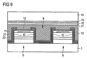
図9に示されている介在ステップにおいては、支持体14が、成長基板1と半導体8からなる接合部と接続され、この場合ハンダ層の第1部分とハンダ層の第2部分が溶融されてハンダ層13になる。このハンダ層13は、半導体8の間のトレンチ9を完全に充たしている。
In the intervening step shown in FIG. 9, the
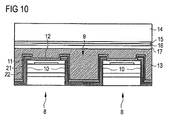
図10に示されている介在ステップでは、成長基板が半導体8から剥離されている。
In the intervening step shown in FIG. 10, the growth substrate is separated from the
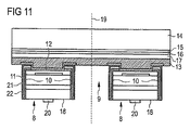
図11に示されている介在ステップでは、ハンダ層13が、半導体8の間のトレンチ9から除去され、さらに支持体14は、場合によって半導体8の間のトレンチ9に沿った分断によって個々の半導体素子に個別化されている。
In the intervening step shown in FIG. 11, the
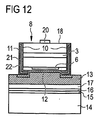
そのようにして製造されたオプトエレクトロニクス半導体素子は図12に示されている。このオプトエレクトロニクス半導体素子の半導体8は、成長基板を有していないだけではなく、有利には、もとの成長基板とは反対側において支持体14と接続される。この支持体14は、特にその熱的特性と電気的特性に関してその際の成長基板に対する結晶構造化と格子定数への厳しい要求を満たすことなく最適化され得る。特に前記支持体14はゲルマニウム支持体であってもよい。
The optoelectronic semiconductor device thus manufactured is shown in FIG. The
オプトエレクトロニクス半導体素子の半導体8の側方縁部10は、有利には、ミラー層21に基づいて半導体8の活性層3から放射される電磁ビームに対して高い反射性を有し得る。この活性層3から側方縁部10方向に放射される電磁ビームは、有利にはミラー層21によって反射され、場合によっては、1つ若しくは複数のさらなる反射の後で半導体8のビーム出射側18から出力される。さらに支持体14の方向へ放射されるビームが有利には反射性コンタクト層6によってビーム出力結合面18の方向へ反射される。それ故にこのオプトエレクトロニクス半導体素子は、ビーム出力結合側方向へのより良好な光出力によって抜きんでる。
The
当該方法並びにオプトエレクトロニクス半導体素子のさらなる利点及び有利な改善例は、先に説明した第1実施例に相応する。 Further advantages and advantageous improvements of the method and of the optoelectronic semiconductor device correspond to the first embodiment described above.
本発明は、実施例の記載によって限定されない。むしろ、あらゆる新規な特性とその新規な特性の組み合わせが本発明に包含される。例え、その特性または組み合わせそのものが、特許請求の範囲あるいは実施例に明確に定義されていなかったとしても、特許請求の範囲に記載されたあらゆる特性の組み合わせが本発明に包含される。 The present invention is not limited by the description of the examples. Rather, all novel properties and combinations of the novel properties are encompassed by the present invention. Even if the characteristics or combinations themselves are not clearly defined in the claims or examples, all combinations of the characteristics described in the claims are included in the present invention.
Claims (15)
成長基板(1)上にエピタキシャル層列(5)を成長させるステップと、
前記エピタキシャル層列(5)の成長基板(1)とは反対側表面に、コンタクト層(6)とそれに続くバリア層(7)とを被着するステップと、
前記エピタキシャル層列(5)内に複数のトレンチを形成することによって前記エピタキシャル層列(5)を個別の半導体(8)に構造化するステップと、
前記トレンチ内に露出する半導体(8)の少なくとも側方縁部(10)に、誘電層(11)を被着するステップと、
前記半導体(8)の間のトレンチ(9)内でハンダ層(13)の第1部分(13a)を半導体(8)へ被着するステップと、
ハンダ層(13)の第2部分(13b)を支持体(14)に被着するステップと、
前記半導体(8)を、成長基板(1)とは反対側において、ハンダ層(13)を用いて支持体(14)に接続させるステップとを有し、この場合、ハンダ層(13)の第1部分(13a)と第2部分(13b)とが相互に溶融され、半導体(8)間の複数のトレンチ(9)がハンダ層(13)によって充填され、さらに、
成長基板(1)を剥離するステップとを有することを特徴とする方法。 In the manufacturing method of the optoelectronic semiconductor element,
Growing an epitaxial layer sequence (5) on a growth substrate (1);
Depositing a contact layer (6) and a subsequent barrier layer (7) on the surface of the epitaxial layer sequence (5) opposite to the growth substrate (1);
Structuring the epitaxial layer sequence (5) into individual semiconductors (8) by forming a plurality of trenches in the epitaxial layer sequence (5);
Depositing a dielectric layer (11) on at least the side edge (10) of the semiconductor (8) exposed in the trench;
Depositing the first part (13a) of the solder layer (13) on the semiconductor (8) in the trench (9) between the semiconductors (8);
Applying the second part (13b) of the solder layer (13) to the support (14);
Connecting the semiconductor (8) to the support (14) using a solder layer (13) on the side opposite to the growth substrate (1). In this case, the first step of the solder layer (13) The first part (13a) and the second part (13b) are melted together, and a plurality of trenches (9) between the semiconductors (8) are filled with the solder layer (13),
Peeling off the growth substrate (1).
前記半導体(8)が、ハンダ層(13)を用いて支持体(14)の主平面と接続されており、
前記半導体(8)の側方縁部(10)が誘電層(11)を備えており、さらに該誘電層(11)にミラー層(21)が被着されていることを特徴とする、オプトエレクトロニクス半導体素子。 An optoelectronic semiconductor device comprising a semiconductor (8),
The semiconductor (8) is connected to the main plane of the support (14) using a solder layer (13);
The semiconductor (8) includes a dielectric layer (11) at a lateral edge (10), and a mirror layer (21) attached to the dielectric layer (11). Electronics semiconductor element.
Applications Claiming Priority (3)
| Application Number | Priority Date | Filing Date | Title |
|---|---|---|---|
| DE102008050573A DE102008050573A1 (en) | 2008-10-06 | 2008-10-06 | Method for producing an optoelectronic semiconductor component and optoelectronic semiconductor component |
| DE102008050573.0 | 2008-10-06 | ||
| PCT/DE2009/001269 WO2010040331A1 (en) | 2008-10-06 | 2009-09-08 | Method for producing an optoelectronic semiconductor component and optoelectronic semiconductor component |
Publications (2)
| Publication Number | Publication Date |
|---|---|
| JP2012504875A true JP2012504875A (en) | 2012-02-23 |
| JP2012504875A5 JP2012504875A5 (en) | 2012-10-25 |
Family
ID=41522173
Family Applications (1)
| Application Number | Title | Priority Date | Filing Date |
|---|---|---|---|
| JP2011530360A Pending JP2012504875A (en) | 2008-10-06 | 2009-09-08 | Optoelectronic semiconductor device manufacturing method and optoelectronic semiconductor device |
Country Status (7)
| Country | Link |
|---|---|
| US (1) | US8367438B2 (en) |
| EP (1) | EP2332183A1 (en) |
| JP (1) | JP2012504875A (en) |
| KR (1) | KR20110082540A (en) |
| CN (1) | CN102171845B (en) |
| DE (1) | DE102008050573A1 (en) |
| WO (1) | WO2010040331A1 (en) |
Cited By (4)
| Publication number | Priority date | Publication date | Assignee | Title |
|---|---|---|---|---|
| JP2018508971A (en) * | 2014-12-19 | 2018-03-29 | グロ アーベーGlo Ab | Method for generating a light emitting diode array on a backplane |
| US10693051B2 (en) | 2016-04-04 | 2020-06-23 | Glo Ab | Through backplane laser irradiation for die transfer |
| JP2021170596A (en) * | 2020-04-15 | 2021-10-28 | 国立大学法人東海国立大学機構 | Manufacturing method of gallium nitride semiconductor device |
| JP2021170594A (en) * | 2020-04-15 | 2021-10-28 | 株式会社デンソー | Semiconductor chips and their manufacturing methods |
Families Citing this family (13)
| Publication number | Priority date | Publication date | Assignee | Title |
|---|---|---|---|---|
| US6909111B2 (en) * | 2000-12-28 | 2005-06-21 | Semiconductor Energy Laboratory Co., Ltd. | Method of manufacturing a light emitting device and thin film forming apparatus |
| JP5754173B2 (en) * | 2011-03-01 | 2015-07-29 | ソニー株式会社 | Light emitting unit and display device |
| TW201318215A (en) * | 2011-10-18 | 2013-05-01 | Chi Mei Lighting Tech Corp | Light-emitting diode and manufacturing method thereof |
| TW201351699A (en) * | 2012-06-05 | 2013-12-16 | Lextar Electronics Corp | Light-emitting diode and manufacturing method thereof |
| DE102012107921A1 (en) * | 2012-08-28 | 2014-03-06 | Osram Opto Semiconductors Gmbh | Method for producing an optoelectronic semiconductor chip |
| DE102013103079A1 (en) * | 2013-03-26 | 2014-10-02 | Osram Opto Semiconductors Gmbh | Optoelectronic semiconductor chip and method for producing an optoelectronic semiconductor chip |
| DE102013109316A1 (en) | 2013-05-29 | 2014-12-04 | Osram Opto Semiconductors Gmbh | Method for producing a plurality of optoelectronic semiconductor chips and optoelectronic semiconductor chip |
| DE102013107531A1 (en) * | 2013-07-16 | 2015-01-22 | Osram Opto Semiconductors Gmbh | Optoelectronic semiconductor chip |
| KR102327141B1 (en) * | 2014-11-19 | 2021-11-16 | 삼성전자주식회사 | Pre-package and manufacturing method of semiconductor package using the same |
| KR20170133347A (en) * | 2015-03-30 | 2017-12-05 | 소니 세미컨덕터 솔루션즈 가부시키가이샤 | Light emitting device, light emitting unit, light emitting panel device, and driving method of light emitting panel device |
| DE102017106508A1 (en) * | 2017-03-27 | 2018-09-27 | Osram Opto Semiconductors Gmbh | Optoelectronic semiconductor device and manufacturing method |
| CN107910405B (en) * | 2017-09-27 | 2019-08-23 | 华灿光电(浙江)有限公司 | Manufacturing method of light emitting diode chip |
| CN111769438B (en) * | 2019-04-02 | 2021-10-15 | 苏州长瑞光电有限公司 | Surface emitting laser device |
Citations (4)
| Publication number | Priority date | Publication date | Assignee | Title |
|---|---|---|---|---|
| JPH07106631A (en) * | 1993-09-29 | 1995-04-21 | Sanken Electric Co Ltd | Semiconductor light emission element |
| US20060237735A1 (en) * | 2005-04-22 | 2006-10-26 | Jean-Yves Naulin | High-efficiency light extraction structures and methods for solid-state lighting |
| JP2007103460A (en) * | 2005-09-30 | 2007-04-19 | Sanyo Electric Co Ltd | Semiconductor laser device and its manufacturing method |
| JP2008118125A (en) * | 2006-10-13 | 2008-05-22 | Sanyo Electric Co Ltd | Semiconductor light emitting device, lighting device, and method for manufacturing semiconductor light emitting device |
Family Cites Families (14)
| Publication number | Priority date | Publication date | Assignee | Title |
|---|---|---|---|---|
| US5972157A (en) * | 1995-11-20 | 1999-10-26 | Alliedsignal Inc. | Joining of rough carbon-carbon composites with high joint strength |
| DE10059532A1 (en) * | 2000-08-08 | 2002-06-06 | Osram Opto Semiconductors Gmbh | Semiconductor chip for use with a luminous diode in optoelectronics, has an active layer with a zone to emit photons fixed on a fastening side on a carrier body |
| US20020017652A1 (en) * | 2000-08-08 | 2002-02-14 | Stefan Illek | Semiconductor chip for optoelectronics |
| TWI226139B (en) | 2002-01-31 | 2005-01-01 | Osram Opto Semiconductors Gmbh | Method to manufacture a semiconductor-component |
| KR101030068B1 (en) * | 2002-07-08 | 2011-04-19 | 니치아 카가쿠 고교 가부시키가이샤 | Nitride semiconductor device manufacturing method and nitride semiconductor device |
| US6929966B2 (en) * | 2002-11-29 | 2005-08-16 | Osram Opto Semiconductors Gmbh | Method for producing a light-emitting semiconductor component |
| DE10307280B4 (en) * | 2002-11-29 | 2005-09-01 | Osram Opto Semiconductors Gmbh | Method for producing a light-emitting semiconductor component |
| US7372077B2 (en) * | 2003-02-07 | 2008-05-13 | Sanyo Electric Co., Ltd. | Semiconductor device |
| JP4868709B2 (en) * | 2004-03-09 | 2012-02-01 | 三洋電機株式会社 | Light emitting element |
| US7208334B2 (en) * | 2004-03-31 | 2007-04-24 | Kabushiki Kaisha Toshiba | Method of manufacturing semiconductor device, acid etching resistance material and copolymer |
| CN100388517C (en) * | 2004-07-08 | 2008-05-14 | 夏普株式会社 | Nitride-based compound semiconductor light-emitting element and manufacturing method thereof |
| JP4906256B2 (en) * | 2004-11-10 | 2012-03-28 | 株式会社沖データ | Manufacturing method of semiconductor composite device |
| DE102005029246B4 (en) | 2005-03-31 | 2023-06-22 | OSRAM Opto Semiconductors Gesellschaft mit beschränkter Haftung | Semiconductor chip with a solder layer sequence and method for soldering a semiconductor chip |
| KR100856230B1 (en) * | 2007-03-21 | 2008-09-03 | 삼성전기주식회사 | Light emitting device, manufacturing method and monolithic light emitting diode array |
-
2008
- 2008-10-06 DE DE102008050573A patent/DE102008050573A1/en not_active Ceased
-
2009
- 2009-09-08 EP EP09740635A patent/EP2332183A1/en not_active Withdrawn
- 2009-09-08 WO PCT/DE2009/001269 patent/WO2010040331A1/en not_active Ceased
- 2009-09-08 US US13/122,578 patent/US8367438B2/en not_active Expired - Fee Related
- 2009-09-08 KR KR1020117010118A patent/KR20110082540A/en not_active Withdrawn
- 2009-09-08 CN CN200980139340XA patent/CN102171845B/en not_active Expired - Fee Related
- 2009-09-08 JP JP2011530360A patent/JP2012504875A/en active Pending
Patent Citations (4)
| Publication number | Priority date | Publication date | Assignee | Title |
|---|---|---|---|---|
| JPH07106631A (en) * | 1993-09-29 | 1995-04-21 | Sanken Electric Co Ltd | Semiconductor light emission element |
| US20060237735A1 (en) * | 2005-04-22 | 2006-10-26 | Jean-Yves Naulin | High-efficiency light extraction structures and methods for solid-state lighting |
| JP2007103460A (en) * | 2005-09-30 | 2007-04-19 | Sanyo Electric Co Ltd | Semiconductor laser device and its manufacturing method |
| JP2008118125A (en) * | 2006-10-13 | 2008-05-22 | Sanyo Electric Co Ltd | Semiconductor light emitting device, lighting device, and method for manufacturing semiconductor light emitting device |
Cited By (6)
| Publication number | Priority date | Publication date | Assignee | Title |
|---|---|---|---|---|
| JP2018508971A (en) * | 2014-12-19 | 2018-03-29 | グロ アーベーGlo Ab | Method for generating a light emitting diode array on a backplane |
| US10693051B2 (en) | 2016-04-04 | 2020-06-23 | Glo Ab | Through backplane laser irradiation for die transfer |
| JP2021170596A (en) * | 2020-04-15 | 2021-10-28 | 国立大学法人東海国立大学機構 | Manufacturing method of gallium nitride semiconductor device |
| JP2021170594A (en) * | 2020-04-15 | 2021-10-28 | 株式会社デンソー | Semiconductor chips and their manufacturing methods |
| JP7477835B2 (en) | 2020-04-15 | 2024-05-02 | 株式会社デンソー | Semiconductor chip manufacturing method |
| JP7553915B2 (en) | 2020-04-15 | 2024-09-19 | 国立大学法人東海国立大学機構 | Method for manufacturing a gallium nitride semiconductor device |
Also Published As
| Publication number | Publication date |
|---|---|
| CN102171845B (en) | 2013-07-31 |
| EP2332183A1 (en) | 2011-06-15 |
| CN102171845A (en) | 2011-08-31 |
| US8367438B2 (en) | 2013-02-05 |
| US20110186953A1 (en) | 2011-08-04 |
| DE102008050573A1 (en) | 2010-04-08 |
| WO2010040331A1 (en) | 2010-04-15 |
| KR20110082540A (en) | 2011-07-19 |
Similar Documents
| Publication | Publication Date | Title |
|---|---|---|
| JP2012504875A (en) | Optoelectronic semiconductor device manufacturing method and optoelectronic semiconductor device | |
| JP5883118B2 (en) | Optoelectronic semiconductor chip | |
| KR101623986B1 (en) | Optoelectronic component and method for producing a plurality of optoelectronic components | |
| CN107924974B (en) | Optoelectronic semiconductor component and method for the production thereof | |
| KR101457247B1 (en) | Photoelectric device | |
| TWI317180B (en) | Optoelectronic component, device with several optoelectronic components and method to produce an optoelectronic component | |
| KR102276207B1 (en) | Semiconductor light-emitting element and semiconductor light-emitting device | |
| JP5759004B2 (en) | Optoelectronic semiconductor chip | |
| US8088649B2 (en) | Radiation-emitting semiconductor body with carrier substrate and method for the producing the same | |
| JP6419077B2 (en) | Wavelength conversion light emitting device | |
| KR101325397B1 (en) | Method for laterally cutting through a semiconductor wafer and optoelectronic component | |
| KR20110019416A (en) | Optoelectronic component and method for the production thereof | |
| JP2000277804A (en) | Method for manufacturing nitride semiconductor device, nitride semiconductor device, and light emitting device | |
| KR20150056559A (en) | Optoelectronic semiconductor chip having a plurality of active regions arranged alongside one another | |
| EP2601692A1 (en) | Light-emitting diode chip | |
| US20170236980A1 (en) | Optoelectronic Semiconductor Chip and Method for Producing the Same | |
| KR101249432B1 (en) | Method for producing a thin-film semiconductor chip | |
| JP2009510733A (en) | Optoelectronic semiconductor chip and method for manufacturing the chip | |
| JP4570683B2 (en) | Nitride compound semiconductor light emitting device manufacturing method | |
| TW201618327A (en) | Photoelectric semiconductor wafer and method of manufacturing same |
Legal Events
| Date | Code | Title | Description |
|---|---|---|---|
| A521 | Request for written amendment filed |
Free format text: JAPANESE INTERMEDIATE CODE: A523 Effective date: 20120904 |
|
| A621 | Written request for application examination |
Free format text: JAPANESE INTERMEDIATE CODE: A621 Effective date: 20120904 |
|
| A977 | Report on retrieval |
Free format text: JAPANESE INTERMEDIATE CODE: A971007 Effective date: 20130814 |
|
| A131 | Notification of reasons for refusal |
Free format text: JAPANESE INTERMEDIATE CODE: A131 Effective date: 20130819 |
|
| A601 | Written request for extension of time |
Free format text: JAPANESE INTERMEDIATE CODE: A601 Effective date: 20131106 |
|
| A602 | Written permission of extension of time |
Free format text: JAPANESE INTERMEDIATE CODE: A602 Effective date: 20131113 |
|
| A521 | Request for written amendment filed |
Free format text: JAPANESE INTERMEDIATE CODE: A523 Effective date: 20140204 |
|
| A02 | Decision of refusal |
Free format text: JAPANESE INTERMEDIATE CODE: A02 Effective date: 20140303 |