JP2012504235A - Nitrogen oxide gas sensor with long-term signal stability - Google Patents
Nitrogen oxide gas sensor with long-term signal stability Download PDFInfo
- Publication number
- JP2012504235A JP2012504235A JP2011528952A JP2011528952A JP2012504235A JP 2012504235 A JP2012504235 A JP 2012504235A JP 2011528952 A JP2011528952 A JP 2011528952A JP 2011528952 A JP2011528952 A JP 2011528952A JP 2012504235 A JP2012504235 A JP 2012504235A
- Authority
- JP
- Japan
- Prior art keywords
- film
- type semiconductor
- metal oxide
- gas sensor
- semiconductor metal
- Prior art date
- Legal status (The legal status is an assumption and is not a legal conclusion. Google has not performed a legal analysis and makes no representation as to the accuracy of the status listed.)
- Ceased
Links
Images


Classifications
-
- G—PHYSICS
- G01—MEASURING; TESTING
- G01N—INVESTIGATING OR ANALYSING MATERIALS BY DETERMINING THEIR CHEMICAL OR PHYSICAL PROPERTIES
- G01N27/00—Investigating or analysing materials by the use of electric, electrochemical, or magnetic means
- G01N27/26—Investigating or analysing materials by the use of electric, electrochemical, or magnetic means by investigating electrochemical variables; by using electrolysis or electrophoresis
- G01N27/403—Cells and electrode assemblies
- G01N27/406—Cells and probes with solid electrolytes
- G01N27/407—Cells and probes with solid electrolytes for investigating or analysing gases
- G01N27/4073—Composition or fabrication of the solid electrolyte
- G01N27/4074—Composition or fabrication of the solid electrolyte for detection of gases other than oxygen
-
- G—PHYSICS
- G01—MEASURING; TESTING
- G01N—INVESTIGATING OR ANALYSING MATERIALS BY DETERMINING THEIR CHEMICAL OR PHYSICAL PROPERTIES
- G01N27/00—Investigating or analysing materials by the use of electric, electrochemical, or magnetic means
- G01N27/26—Investigating or analysing materials by the use of electric, electrochemical, or magnetic means by investigating electrochemical variables; by using electrolysis or electrophoresis
- G01N27/403—Cells and electrode assemblies
- G01N27/406—Cells and probes with solid electrolytes
- G01N27/4065—Circuit arrangements specially adapted therefor
Abstract
本発明は、一酸化窒素と二酸化窒素とを同時に測定し、測定精度及び長期安定性を確保できる窒素酸化物ガスセンサーを提供する。すなわち、酸素イオン伝導性の固体電解質と、固体電解質と接し、p型半導体金属酸化物で形成された第1膜と、固体電解質と接し、p型半導体金属酸化物で形成された第2膜と、第1膜及び第2膜のうち少なくとも一つに含まれたn型半導体金属酸化物と、第1ノードは、第1膜と電気的に連結され、第2ノードは、第2膜と電気的に連結され、第1膜及び第2膜に電流を印加する電源と、第1ノードと第2ノードとの電位差を測定する測定部と、を備える窒素酸化物ガスセンサーである。
【選択図】図1The present invention provides a nitrogen oxide gas sensor capable of simultaneously measuring nitrogen monoxide and nitrogen dioxide and ensuring measurement accuracy and long-term stability. Specifically, an oxygen ion conductive solid electrolyte, a first film in contact with the solid electrolyte and formed of p-type semiconductor metal oxide, and a second film in contact with the solid electrolyte and formed of p-type semiconductor metal oxide The n-type semiconductor metal oxide included in at least one of the first film and the second film is electrically connected to the first film, and the second node is electrically connected to the second film. The nitrogen oxide gas sensor includes a power source for applying current to the first film and the second film, and a measurement unit for measuring a potential difference between the first node and the second node.
[Selection] Figure 1
Description
本発明は、窒素酸化物ガスセンサーに係り、特に長期安定性を確保できる窒素酸化物ガスセンサーに関する。 The present invention relates to a nitrogen oxide gas sensor, and more particularly to a nitrogen oxide gas sensor that can ensure long-term stability.
窒素酸化物ガスは、一酸化窒素(NO)、二酸化窒素(NO2)及び亜酸化窒素(N2O)を含めてNOxとして表示する。そのうち、一酸化窒素及び二酸化窒素が窒素酸化物ガスのほとんどを占め、それらは、大気汚染源として作用して、その濃度を測定して排出量を適切に制御する必要がある。 Nitrogen oxide gas is displayed as NOx including nitric oxide (NO), nitrogen dioxide (NO 2 ), and nitrous oxide (N 2 O). Of these, nitric oxide and nitrogen dioxide account for most of the nitrogen oxide gas, which acts as an air pollution source and needs to measure its concentration to control emissions appropriately.
既存の窒素酸化物の濃度を測定する方法としては、平衡電位を利用する方法がある。この方法では、固体電解質に、固体の硝酸塩を感知電極として形成するとともに、固体電解質内のイオン活動度を一定にする貴金属電極を形成して、電気化学セルを形成することで、このセルで発生する起電力を利用して窒素酸化物の濃度を測定する。しかし、この方法では、感知電極の溶融点が低く、高温のガスに対して適用しがたいという限界がある。 As a method for measuring the concentration of existing nitrogen oxides, there is a method using an equilibrium potential. In this method, solid nitrate is formed as a sensing electrode on the solid electrolyte, and a noble metal electrode that makes the ionic activity in the solid electrolyte constant is formed to form an electrochemical cell. The concentration of nitrogen oxides is measured using the electromotive force. However, this method has a limitation that the sensing electrode has a low melting point and is difficult to apply to a high-temperature gas.
窒素酸化物の濃度を測定する他の方法としては、電流式センサーがある。これは、酸素ポンピングセルを利用して二酸化窒素を一酸化窒素に変換し、この一酸化窒素を分解して得られた酸素イオンによる電流を測定して、窒素酸化物の濃度を測定するものである。しかし、この方法では、酸素ポンピングセルを利用せねばならない構造的限界があり、酸素イオンによる電流測定自体が、温度による変化が大きく、濃度が数百ppm以下である条件では、測定電流が非常に小さくなって、窒素酸化物の総量を測定しがたいという限界がある。 Another method for measuring the concentration of nitrogen oxide is a current sensor. This is to measure the concentration of nitrogen oxides by converting nitrogen dioxide into nitrogen monoxide using an oxygen pumping cell and measuring the current due to oxygen ions obtained by decomposing the nitrogen monoxide. is there. However, this method has a structural limitation that requires the use of an oxygen pumping cell, and the current measurement using oxygen ions itself is very changeable with temperature, and the measurement current is very low under conditions where the concentration is several hundred ppm or less. There is a limit that it becomes difficult to measure the total amount of nitrogen oxides.
窒素酸化物の濃度を測定するさらに他の方法としては、混合電位方式がある。これは、酸素イオン伝導性の固体電解質の一側面に金属酸化物で感知電極を形成し、固体電解質の他側面に貴金属で基準電極を形成して、感知電極と基準電極との電位差を測定するものである。すなわち、前記感知電極は、窒素酸化物と酸素とに対する反応性を有するが、基準電極は、酸素にのみ反応性を有するので、ガス中に含まれた窒素酸化物の濃度によって、感知電極と基準電極との電位差が発生するので、この電位差を測定することで、窒素酸化物の濃度を測定する。しかし、この方式の場合、二酸化窒素と一酸化窒素との分解反応によって発生する起電力符号の差によって、二酸化窒素と一酸化窒素とが混在する窒素酸化物ガスに対しては、測定精度が非常に低下するという問題がある。 As yet another method for measuring the concentration of nitrogen oxide, there is a mixed potential method. In this method, a sensing electrode is formed with a metal oxide on one side of an oxygen ion conductive solid electrolyte, a reference electrode is formed with a noble metal on the other side of the solid electrolyte, and a potential difference between the sensing electrode and the reference electrode is measured. Is. That is, the sensing electrode has reactivity with nitrogen oxides and oxygen, but the reference electrode has reactivity only with oxygen, and therefore, the sensing electrode and the reference electrode depend on the concentration of nitrogen oxides contained in the gas. Since a potential difference with the electrode is generated, the concentration of nitrogen oxides is measured by measuring this potential difference. However, in this method, the measurement accuracy is very high for nitrogen oxide gas in which nitrogen dioxide and nitrogen monoxide are mixed due to the difference in electromotive force sign generated by the decomposition reaction between nitrogen dioxide and nitric oxide. There is a problem that it drops.
この問題を解決するために、窒素酸化物を一つのガス形態に変換する変換セルを利用する方法が提案されているが、窒素酸化物の全体を一酸化窒素または二酸化窒素に変換するのには限界があり、窒素酸化物の全体濃度を測定しがたいという問題がある。 In order to solve this problem, a method using a conversion cell that converts nitrogen oxides into a single gas form has been proposed, but in order to convert the entire nitrogen oxides into nitrogen monoxide or nitrogen dioxide. There is a limit and there is a problem that it is difficult to measure the total concentration of nitrogen oxides.
本発明の目的は、一酸化窒素と二酸化窒素とを同時に測定し、測定精度及び長期安定性を確保できる窒素酸化物ガスセンサーを提供するところにある。 An object of the present invention is to provide a nitrogen oxide gas sensor capable of simultaneously measuring nitrogen monoxide and nitrogen dioxide and ensuring measurement accuracy and long-term stability.
前記目的を達成するために、本発明は、酸素イオン伝導性の固体電解質と、前記固体電解質と接し、p型半導体金属酸化物で形成された第1膜と、前記固体電解質と接し、p型半導体金属酸化物で形成された第2膜と、前記第1膜及び第2膜のうち少なくとも一つに含まれたn型半導体金属酸化物と、第1ノードは、前記第1膜と電気的に連結され、第2ノードは、前記第2膜と電気的に連結され、前記第1膜及び第2膜に電流を印加する電源と、前記第1ノードと第2ノードとの電位差を測定する測定部と、を備える窒素酸化物ガスセンサーを提供する。 To achieve the above object, the present invention provides an oxygen ion conductive solid electrolyte, a first film in contact with the solid electrolyte, formed of a p-type semiconductor metal oxide, in contact with the solid electrolyte, and p-type. A second film formed of a semiconductor metal oxide; an n-type semiconductor metal oxide included in at least one of the first film and the second film; and a first node electrically connected to the first film. The second node is electrically connected to the second film and measures a potential difference between the first node and the second node and a power source for applying a current to the first film and the second film. And a nitrogen oxide gas sensor comprising a measurement unit.
本発明の他の特徴によれば、前記n型半導体金属酸化物は、前記第1膜及び第2膜のうち少なくとも一つの前記p型半導体金属酸化物と混合される。 The n-type semiconductor metal oxide may be mixed with at least one of the first and second films of the p-type semiconductor metal oxide.
本発明のさらに他の特徴によれば、前記n型半導体金属酸化物は、前記第1膜及び第2膜のうち少なくとも一つの前記p型半導体金属酸化物と固溶体化される。 According to still another aspect of the present invention, the n-type semiconductor metal oxide is solid-solutioned with at least one of the first and second films.
本発明のさらに他の特徴によれば、前記第1膜及び第2膜のうち、前記n型半導体金属酸化物を含む膜は、p型半導体金属酸化物で形成された膜と、前記n型半導体金属酸化物を含むバッファ膜との積層体で形成される。 According to still another aspect of the present invention, the film including the n-type semiconductor metal oxide among the first film and the second film includes a film formed of a p-type semiconductor metal oxide, and the n-type semiconductor metal oxide. It is formed of a stacked body with a buffer film containing a semiconductor metal oxide.
本発明のさらに他の特徴によれば、前記バッファ膜は、前記n型半導体金属酸化物とp型半導体金属酸化物との固溶体で形成される。 The buffer film may be formed of a solid solution of the n-type semiconductor metal oxide and the p-type semiconductor metal oxide.
本発明のさらに他の特徴によれば、前記バッファ膜は、前記n型半導体金属酸化物とp型半導体金属酸化物との混合物で形成される。 The buffer film may be formed of a mixture of the n-type semiconductor metal oxide and the p-type semiconductor metal oxide.
本発明のさらに他の特徴によれば、前記第1膜の前記固体電解質に対向した面に形成され、導電性金属で形成された第1電極をさらに備える。 According to still another aspect of the present invention, it further includes a first electrode formed on a surface of the first film facing the solid electrolyte and made of a conductive metal.
本発明のさらに他の特徴によれば、前記固体電解質と接し、導電性金属で形成され、前記電源に対して前記第1膜と並列に連結された第3膜をさらに備える。 According to still another aspect of the present invention, the apparatus further includes a third film that is in contact with the solid electrolyte, is formed of a conductive metal, and is connected to the power supply in parallel with the first film.
本発明のさらに他の特徴によれば、前記第1電極及び第3膜は、一体に形成される。 According to still another aspect of the present invention, the first electrode and the third film are integrally formed.
本発明のさらに他の特徴によれば、前記第1電極及び第3膜は、貴金属で形成される。 According to still another aspect of the present invention, the first electrode and the third film are made of a noble metal.
本発明のさらに他の特徴によれば、前記第2膜の前記固体電解質に対向した面に形成され、導電性金属で形成された第2電極をさらに備える。 According to still another aspect of the present invention, the apparatus further includes a second electrode formed on a surface of the second film facing the solid electrolyte and made of a conductive metal.
本発明のさらに他の特徴によれば、前記固体電解質と接し、導電性金属で形成され、前記電源に対して前記第2膜と並列に連結された第4膜をさらに備える。 According to still another aspect of the present invention, the apparatus further includes a fourth film that is in contact with the solid electrolyte, is formed of a conductive metal, and is connected to the power supply in parallel with the second film.
本発明のさらに他の特徴によれば、前記第2電極及び第4膜は、一体に形成される。 According to still another feature of the present invention, the second electrode and the fourth film are integrally formed.
本発明のさらに他の特徴によれば、前記第2電極及び第4膜は、貴金属で形成される。 According to still another aspect of the present invention, the second electrode and the fourth film are made of a noble metal.
本発明によれば、第1膜及び第2膜により一酸化窒素と二酸化窒素とを同時に測定できる。 According to the present invention, nitrogen monoxide and nitrogen dioxide can be simultaneously measured by the first film and the second film.
また、第1膜と並列に連結された第3膜、第2膜と並列に連結された第4膜により測定精度を高めることができる。 In addition, measurement accuracy can be improved by the third film connected in parallel with the first film and the fourth film connected in parallel with the second film.
そして、第1膜にp型半導体金属酸化物、第2膜に他のp型半導体金属酸化物を使用し、これに加えて、第1膜及び第2膜のうち少なくとも一つにn型半導体金属酸化物を含むことで、長期安定性を確保できる。 In addition, a p-type semiconductor metal oxide is used for the first film, and another p-type semiconductor metal oxide is used for the second film. In addition, at least one of the first film and the second film is an n-type semiconductor. Long-term stability can be ensured by including a metal oxide.
以下、本発明の望ましい実施形態を説明する。しかし、本発明の実施形態は、色々な他の形態に変形され、本発明の範囲が後述する実施形態により限定されるものと解釈されてはならない。本発明の実施形態は、当業者に本発明をより完全に説明するために提供されるものである。 Hereinafter, preferred embodiments of the present invention will be described. However, the embodiments of the present invention can be modified into various other forms, and the scope of the present invention should not be construed as being limited by the embodiments described below. Rather, these embodiments are provided so that this disclosure will be thorough and complete, and will fully convey the concept of the invention to those skilled in the art.
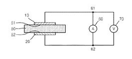
図1は、本発明の望ましい一実施形態による窒素酸化物ガスセンサーを示す概略図である。 FIG. 1 is a schematic view illustrating a nitrogen oxide gas sensor according to an exemplary embodiment of the present invention.
図1を参照すれば、本発明の望ましい一実施形態による窒素酸化物ガスセンサーは、酸素イオン伝導性の固体電解質50、この固体電解質50に接する第1膜10及び第2膜20、電源60及び測定部70を備える。
Referring to FIG. 1, a nitrogen oxide gas sensor according to a preferred embodiment of the present invention includes an oxygen ion conductive
酸素イオン伝導性の固体電解質50は、高温で酸素イオンの伝導が可能なものであって、安定化ジルコニア、CeO2またはThO2で形成される。前記安定化ジルコニアとしては、特にYSZ(Yttria−stabilized
Zirconia:イットリア安定化ジルコニア)が使われる。
The oxygen ion conductive
Zirconia: yttria stabilized zirconia) is used.
かかる固体電解質50の第1領域51には第1膜10が接し、第2領域52には第2膜20が接するようにする。
The
前記第1膜10及び第2膜20は、それらに電源が印加された時に、窒素酸化物と酸素とに対して反応性を有する物質で形成するが、第1膜10は、p型半導体金属酸化物で形成し、第2膜20も、p型半導体金属酸化物で形成する。この時、前記第2膜20は、第1膜10とは異なるp型半導体金属酸化物で形成されるが、必ずしもこれに限定されるものではない。
The
前記第1膜10は、p型半導体金属酸化物で形成されるが、例えば、CuO,NiO,CoO,Cr2O3,Cu2O,MoO2,Ag2O,Bi2O3,Pr2O3,MnO及びLaCoO3からなる群から選択された少なくとも一つ以上の物質、またはそれらの物質を少なくとも二つ以上混合した混合物、またはそれらの物質のうち少なくとも一つと、前記酸素イオン伝導性の固体電解質物質とを混合した混合物を含む。本発明の望ましい一実施形態において、前記第1膜10は、かかるp型半導体金属酸化物のうちNiOを使用することが望ましい。
The
前記固体電解質50の第2領域52には、第2膜20が接する。前記第2膜20も、p型半導体金属酸化物で形成されるが、例えば、CuO,NiO,CoO,Cr2O3,Cu2O,MoO2,Ag2O,Bi2O3,Pr2O3,MnO及びLaCoO3からなる群から選択された少なくとも一つ以上の物質、またはそれらの物質を少なくとも二つ以上混合した混合物、またはそれらの物質のうち少なくとも一つと、前記酸素イオン伝導性の固体電解質物質とを混合した混合物を含む。本発明の望ましい一実施形態によれば、前記第2膜20は、前記第1膜10とは異なるp型半導体金属酸化物で形成され、CuOまたはLaCoO3で形成される。
The
図1において、第1領域51と第2領域52とは、固体電解質50において互いに対向した領域であるが、本発明は、必ずしもこれに限定されるものではなく、固体電解質50の同一平面上の他の領域に位置してもよい。ただし、前記第1領域51と第2領域52とは、互いに重ならないようにすることが望ましい。これについてのさらに詳細な実施形態は後述する。
In FIG. 1, the
かかる第1膜10と第2膜20とは、電源60の第1ノード61及び第2ノード62にそれぞれ電気的に連結されて、一定した電流を印加する。
The
本発明において、前記第1膜10は正の電極として、第2膜20は負の電極として使用できる。
正の電極である第1膜10と固体電解質50との界面には、酸素イオンが酸素ガスに変換するアノード反応が起こり、同時にNOガスが存在する場合、下記反応式1に表すように、NOによるアノード反応が起こり、一定した電流を流すための電圧の大きさを減少させる。この時、第1膜10には、アノード分極が加えられたので、NOに対する反応は増加し、NO2に対する反応は減少する。
In the present invention, the
When the anode reaction in which oxygen ions are converted into oxygen gas occurs at the interface between the
[反応式1]

負の電極である第2膜20と固体電解質50との界面には、酸素ガスが酸素イオンに変換するカソード反応が起こり、同時にNO2ガスが存在する場合、下記反応式2に表すように、NO2によるカソード反応が起こり、一定した電流を流すための電圧の大きさを減少させる。この時、第2膜20には、カソード分極が加えられたので、NO2に対する反応は増加し、NOに対する反応は減少する。
When the cathode reaction in which oxygen gas is converted into oxygen ions occurs at the interface between the negative electrode
[反応式2]
このように、本発明によれば、NOとNO2との混合ガスが存在する場合、二つのガスのいずれに対する測定精度も向上させることができる。 Thus, according to the present invention, when a mixed gas of NO and NO 2 exists, the measurement accuracy for any of the two gases can be improved.
そして、前記第1ノード61及び第2ノード62には、測定部70が連結され、第1ノード61と第2ノード62との電位差を測定する。
A measuring
前記のような構造で、高温状態で窒素酸化物混合ガスに第1膜10及び第2膜20が露出されれば、窒素酸化物ガス内の二酸化窒素及び一酸化窒素の濃度によって電位差が変化しつつ、二酸化窒素と一酸化窒素との濃度和を測定できる。
If the
一方、前記のように、第1膜10と第2膜20とがp型半導体金属酸化物で形成される場合には、センサーの測定不安定性が引き起こされる。これは、第1膜10及び第2膜20がいずれもp型半導体金属酸化物を使用するため、電子の濃度より正孔の濃度が高くなり、これによって、電子の不足によりガス反応速度が次第に遅くなって、一定した電流のための電圧が経時的に上昇するためであると考えられる。かかる問題点を解決するために、感知物質であるp型半導体金属酸化物の電子濃度を高めねばならないが、本発明では、第1膜10及び第2膜20のうち少なくとも一つをp型半導体金属酸化物とn型半導体金属酸化物との固溶体、もしくはp型半導体金属酸化物とn型半導体金属酸化物との混合物として製作するか、または第1膜10及び第2膜20のうち少なくとも一つと固体電解質50との間にn型半導体金属酸化物が含まれたバッファ膜11を介在させた。この時のn型半導体金属酸化物としては、ZnO,MgO,Al2O3,SiO2,V2O5,Fe2O3,SrO,BaO,TiO2,BaTiO3,CeO2,Nb2O5,Ta2O5,Ga2O3及びWO3からなる群から選択される少なくとも一つの金属酸化物、またはそれらの混合物を含む。本発明の望ましい一実施形態によれば、前記n型半導体金属酸化物としてはZnOを使用する。
On the other hand, as described above, when the
したがって、図1による実施形態の場合、第1膜10をp型半導体金属酸化物とn型半導体金属酸化物とを混合させて製作するか、またはp型半導体金属酸化物とn型半導体金属酸化物とを固溶体化して製作する。これにより、第1膜10の長期安定性を確保できる。これは、第1膜10だけでなく、第2膜20にも同一に適用可能なものであって、第2膜20にのみn型半導体金属酸化物を混合または固溶体化させるか、または第1膜10及び第2膜20にいずれもn型半導体金属酸化物を混合または固溶体化させる。この時、前記p型半導体金属酸化物を主として混合または固溶体化してもよく、前記n型半導体金属酸化物を主として混合または固溶体化してもよい。
Therefore, in the embodiment according to FIG. 1, the
前記のようなn型半導体金属酸化物は、図2に示すように、p型半導体金属酸化物で形成された膜11と固体電解質50との間に介在させたバッファ膜12とし、第1膜10は膜11とバッファ膜12との積層体とすることができる。この時、p型半導体金属酸化物で形成された膜11は、前述したように、CuO,NiO,CoO,Cr2O3,Cu2O,MoO2,Ag2O,Bi2O3,Pr2O3,MnO及びLaCoO3からなる群から選択された少なくとも一つ以上の物質、またはそれらの物質を少なくとも二つ以上混合した混合物、またはそれらの物質のうち少なくとも一つと、前記酸素イオン伝導性の固体電解質物質とを混合した混合物で形成される。
As shown in FIG. 2, the n-type semiconductor metal oxide as described above is used as the
そして、バッファ膜12に使われるn型半導体金属酸化物としては、前述したように、ZnO,MgO,Al2O3,SiO2,V2O5,Fe2O3,SrO,BaO,TiO2,BaTiO3,CeO2,Nb2O5,Ta2O5,Ga2O3及びWO3からなる群から選択される少なくとも一つの金属酸化物、またはそれらの混合物を含む。本発明の望ましい一実施形態によれば、前記n型半導体金属酸化物としてはZnOを使用する。
As described above, the n-type semiconductor metal oxide used for the
前記バッファ膜11については、p型半導体金属酸化物とn型半導体金属酸化物との固溶体を使用するか、またはp型半導体金属酸化物とn型半導体金属酸化物との混合物を使用できる。例えば、p型半導体金属酸化物で形成された膜11としてNiOを使用し、ZnOをNiOに固溶させたNiO−ZnO固溶体をバッファ膜12として第1膜10を構成できる。この場合、前記バッファ膜12は、第1膜10の固体電解質50との機械的接合特性をさらに向上させる。
For the
このように、バッファ膜12をp型半導体金属酸化物で形成された膜11と固体電解質50との間に介在させることで、前述した実施形態のようにセンサーの測定不安定性を防止し、第1膜10の劣化を遅らせ、これによって長期安定性を確保できる。
Thus, by interposing the
図2による実施形態では、前記第1膜10のみをp型半導体金属酸化物で形成された膜11とバッファ膜12との積層体で形成されたものと図示したが、本発明は、必ずしもこれに限定されるものではなく、図示していないが、第2膜20もかかる積層体で形成されうることはいうまでもない。
In the embodiment according to FIG. 2, it is illustrated that only the
図1及び図2による実施形態において、前記第1膜10及び第2膜20は、第1ノード61及び第2ノード62とそれぞれワイヤーボンディングされる。すなわち、第1膜10及び第2膜20に導電性ポリマーやその他の導電性部材でボンディングパッドを形成した後、このボンディングパッドにワイヤー電力線を連結させる。
1 and 2, the
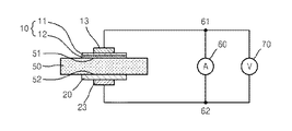
図3及び図4は、それぞれ本発明の望ましいさらに他の実施形態を示すものであって、それぞれ図1及び図2による実施形態において、第1膜10上には、第1電極13が形成され、第1電極13を第1ノード61に電気的に連結させたものであり、第2膜20上にも、第2電極23が形成され、第2電極23を第2ノード62に電気的に連結させたものである。前記第1電極13及び第2電極23は、電気伝導性金属で形成することが望ましいが、さらに望ましくは、腐食環境に耐えるように貴金属で形成する。貴金属としては、金(Au)、銀(Ag)、白金(Pt)、イリジウム(Ir)、パラジウム(Pd)及びそれらの合金から選択された少なくとも一つが適用可能であるが、望ましくは、金や白金が適用可能である。
FIGS. 3 and 4 show still other preferred embodiments of the present invention, respectively. In the embodiments according to FIGS. 1 and 2, a
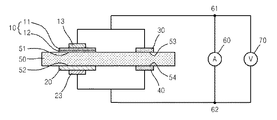
図5及び図6は、それぞれ本発明のさらに他の実施形態を示すものであって、それぞれ図1及び図2による実施形態において、前記固体電解質50の第3領域53と第4領域54とには、それぞれ第3膜30と第4膜40とが接するように設置したものである。第1膜10及び第2膜20は、前述した実施形態と同一であるので、以下では、第3膜30及び第4膜40を中心に説明する。
5 and 6 show still other embodiments of the present invention, respectively. In the embodiments according to FIGS. 1 and 2, respectively, the
第3領域53と第4領域54とは、図5及び図6に示すように互いに対向するが、必ずしもこれに限定されるものではなく、互いに重ならない限り、同一平面上に形成されてもよく、他の平面上に形成されてもよい。
The
前記第3膜30及び第4膜40は、電気伝導性金属で形成されることが望ましいが、さらに望ましくは、腐食環境に耐えるように貴金属で形成する。貴金属としては、金(Au)、銀(Ag)、白金(Pt)、イリジウム(Ir)、パラジウム(Pd)及びそれらの合金から選択された少なくとも一つが適用可能であるが、望ましくは、金や白金が適用可能である。前記のような第3膜30及び第4膜40は、強制的な電流印加により電極に発生する過剰電荷が、第1膜10及び第2膜20と固体電解質との界面に発生するのを、貴金属電極での酸素置換反応により通過させることで、センサー信号の安定性を保証する。
The
この時、前記第3膜30は、前記第1ノード61に電気的に連結して、前記電源60に対して前記第1膜10と並列に連結させる。そして、前記第4膜40は、前記第2ノード62に電気的に連結して、前記電源60に対して前記第2膜20と並列に連結させる。そして、前記第1ノード61及び第2ノード62には、測定部70が連結されて、第1ノード61と第2ノード62との電位差を測定する。
At this time, the
本発明では、このように、第1膜10と第3膜30、第2膜20と第4膜40がそれぞれ並列に連結されて、測定が進められるにつれて測定誤差を減らし、長期安定性を向上させる。これは、第1膜10と第3膜30、第2膜20と第4膜40がそれぞれ並列に連結されることで、測定用電極となる第1膜10と第2膜20とにおける固体電解質50に蓄積される過剰電荷を第3膜30と第4膜40とに分散させることによって可能になると見られるが、必ずしもかかる理由に起因するものと限定されず、その他の複合的または明らかにされていない理由により可能になるものと見られる。
In the present invention, as described above, the
前記第3膜30及び第4膜40は、図5及び図6に示すように、必ずしも単一の膜で存在するものではなく、それぞれが複数の膜で形成されうる。この時、複数の第3膜30は、互いに並列に連結することが望ましく、複数の第4膜40も、互いに並列に連結することが望ましい。
As shown in FIGS. 5 and 6, the
図7は、本発明の望ましいさらに他の実施形態を示すものである。図7に示した実施形態は、図1による実施形態のように、第1膜10と第2膜20とを固体電解質50に形成した後、この固体電解質50上に第1膜10及び第2膜20の少なくとも一部を覆うように、第1導電膜14及び第2導電膜24を薄膜として形成したものである。これらの第1導電膜14及び第2導電膜24は、導電性素材で薄膜状にパターニングでき、第1膜10及び第2膜20の配線の機能を兼ねる。したがって、前記第1導電膜14及び第2導電膜24は、腐食環境に耐えるように貴金属、例えば、金(Au)、銀(Ag)、白金(Pt)、イリジウム(Ir)、パラジウム(Pd)及びそれらの合金から選択された少なくとも一つで形成され、望ましくは、白金ペーストを塗布してパターニングできる。
FIG. 7 shows still another preferred embodiment of the present invention. In the embodiment shown in FIG. 7, after the
この場合、前記第1導電膜14のうち、第1膜10を覆う部分は、図3に示すように、第1膜10上の第1電極の機能を担い、第1導電膜14のうち、固体電解質50の第3領域53に接触する部分は、図5に示すように、第3膜の機能を担う。同様に、前記第2導電膜24のうち、第2膜20を覆う部分は、図3に示すように、第2膜20上の第2電極の機能を担い、第2導電膜24のうち、固体電解質50の第4領域54に接触する部分は、図5に示すように、第4膜の機能を担う。
In this case, the portion of the first
図7に示した第1膜10及び/または第2膜20は、図8に示すように、p型金属酸化物膜11及びバッファ膜12の積層体で形成されうる。その他の構造は、前述した図7の実施形態と同一であるので、省略する。
The
一方、前記第1膜10及び第2膜20は、図9に示すように、固体電解質50の同一平面である第1領域51及び第2領域52と接するように形成されうる。
Meanwhile, as shown in FIG. 9, the
かかる図9による実施形態は、図2ないし図9の実施形態にもいずれも適用可能であることはいうまでもない。 It goes without saying that the embodiment according to FIG. 9 can be applied to any of the embodiments shown in FIGS.
図1ないし図9による実施形態において、第1膜10及び第2膜20は、必ずしも単一の膜で存在するものではなく、それぞれが複数の膜で形成されうる。
In the embodiment according to FIGS. 1 to 9, the
この時、複数の第1膜10は、互いに並列に連結することが望ましく、複数の第2膜20も、互いに並列に連結することが望ましい。
At this time, the plurality of
図10は、図6のような構造を有する窒素酸化物ガスセンサーに対して、NOとNO2との混合ガスに対するセンシング結果を示すものである。CuOを第2膜20とし、第1膜10としては、p型半導体金属酸化物膜11としてNiOを使用し、バッファ膜12としては、ZnOをNiOに固溶させたNiO−ZnO固溶体を使用し、第1電極13、第2電極23、第3膜30及び第4膜40としてPtを使用した。そして、固体電解質50としてはYSZを使用したものである。
FIG. 10 shows a sensing result for a mixed gas of NO and NO 2 with respect to the nitrogen oxide gas sensor having the structure as shown in FIG. CuO is used as the
かかる構造のセンサーに対して、約700℃の温度で酸素分圧を20%とし、2.0μAの一定した電流を印加しつつ電圧を測定した。 With respect to the sensor having such a structure, the voltage was measured while applying a constant current of 2.0 μA at an oxygen partial pressure of 20% at a temperature of about 700 ° C.
図10に示すように、合計四つの試験例において、ほぼ均一な特性が得られ、経時的にも電位値が大きく変化しないということが分かる。 As shown in FIG. 10, it can be seen that substantially uniform characteristics are obtained in a total of four test examples, and the potential value does not change greatly over time.
このように、本発明によれば、窒素酸化物測定センサーを長時間使用する場合にも、その正確度を維持できる。 Thus, according to the present invention, even when the nitrogen oxide measuring sensor is used for a long time, the accuracy can be maintained.
Claims (14)
前記固体電解質と接し、p型半導体金属酸化物で形成された第1膜と、
前記固体電解質と接し、p型半導体金属酸化物で形成された第2膜と、
前記第1膜及び第2膜のうち少なくとも一つに含まれたn型半導体金属酸化物と、
第1ノードは、前記第1膜と電気的に連結され、第2ノードは、前記第2膜と電気的に連結され、前記第1膜及び第2膜に電流を印加する電源と、
前記第1ノードと第2ノードとの電位差を測定する測定部と、を備える窒素酸化物ガスセンサー。 An oxygen ion conductive solid electrolyte;
A first film in contact with the solid electrolyte and formed of a p-type semiconductor metal oxide;
A second film in contact with the solid electrolyte and formed of a p-type semiconductor metal oxide;
An n-type semiconductor metal oxide included in at least one of the first film and the second film;
A first node electrically connected to the first film; a second node electrically connected to the second film; and a power source for applying a current to the first film and the second film;
A nitrogen oxide gas sensor comprising: a measurement unit that measures a potential difference between the first node and the second node.
Applications Claiming Priority (5)
| Application Number | Priority Date | Filing Date | Title |
|---|---|---|---|
| KR10-2008-0096088 | 2008-09-30 | ||
| KR20080096088 | 2008-09-30 | ||
| PCT/KR2009/005613 WO2010038987A2 (en) | 2008-09-30 | 2009-09-30 | Nitrogen-oxide gas sensor with long signal stability |
| KR1020090093054A KR101052618B1 (en) | 2008-09-30 | 2009-09-30 | Nitrogen oxide gas sensor with long term signal stability |
| KR10-2009-0093054 | 2009-09-30 |
Publications (1)
| Publication Number | Publication Date |
|---|---|
| JP2012504235A true JP2012504235A (en) | 2012-02-16 |
Family
ID=42214393
Family Applications (1)
| Application Number | Title | Priority Date | Filing Date |
|---|---|---|---|
| JP2011528952A Ceased JP2012504235A (en) | 2008-09-30 | 2009-09-30 | Nitrogen oxide gas sensor with long-term signal stability |
Country Status (5)
| Country | Link |
|---|---|
| US (1) | US8399883B2 (en) |
| EP (1) | EP2330412A4 (en) |
| JP (1) | JP2012504235A (en) |
| KR (1) | KR101052618B1 (en) |
| WO (1) | WO2010038987A2 (en) |
Cited By (1)
| Publication number | Priority date | Publication date | Assignee | Title |
|---|---|---|---|---|
| JP2016535265A (en) * | 2013-10-31 | 2016-11-10 | シーメンス アクチエンゲゼルシヤフトSiemens Aktiengesellschaft | Gas sensor for detecting nitrogen oxides and method of operating such a gas sensor |
Families Citing this family (8)
| Publication number | Priority date | Publication date | Assignee | Title |
|---|---|---|---|---|
| US20120053861A1 (en) * | 2010-08-26 | 2012-03-01 | Baker Hughes Incorporated | On-line monitoring and prediction of corrosion in overhead systems |
| KR101436358B1 (en) * | 2010-09-03 | 2014-09-02 | 일진머티리얼즈 주식회사 | NOx gas sensor |
| KR101436359B1 (en) * | 2010-09-10 | 2014-09-02 | 일진머티리얼즈 주식회사 | Manufacturing method of NOx gas sensor and NOx gas sensor used thereby |
| DE102011009780A1 (en) * | 2011-01-28 | 2012-08-02 | Continental Automotive Gmbh | Sensor element and method for detecting a parameter of a gas mixture in a gas space |
| US9568448B2 (en) * | 2011-08-25 | 2017-02-14 | Georgia Tech Research Corporation | Gas sensors and methods of preparation thereof |
| EP2839509B1 (en) * | 2012-04-19 | 2020-05-27 | Carnegie Mellon University | A metal-semiconductor-metal (msm) heterojunction diode |
| WO2014039550A1 (en) | 2012-09-04 | 2014-03-13 | Carnegie Mellon University | A hot-electron transistor having metal terminals |
| GB2516932B (en) * | 2013-08-07 | 2018-12-26 | Nokia Technologies Oy | An apparatus and associated methods for water detection |
Citations (7)
| Publication number | Priority date | Publication date | Assignee | Title |
|---|---|---|---|---|
| JPH07198671A (en) * | 1993-12-29 | 1995-08-01 | Riken Corp | Nitrogen oxide sensor |
| JPH07225214A (en) * | 1994-02-14 | 1995-08-22 | Shimadzu Corp | Nox measuring apparatus |
| JPH08247992A (en) * | 1995-03-10 | 1996-09-27 | Riken Corp | Nitrogen oxide sensor |
| JPH11242014A (en) * | 1998-02-25 | 1999-09-07 | Toyota Central Res & Dev Lab Inc | Nitrogen oxide sensor |
| JPH11510908A (en) * | 1996-06-12 | 1999-09-21 | ローベルト ボツシユ ゲゼルシヤフト ミツト ベシユレンクテル ハフツング | Sensor for measuring the concentration of oxidizable components in gas mixtures |
| JP2000321238A (en) * | 1996-09-17 | 2000-11-24 | Riken Corp | Gas sensor |
| JP2001194337A (en) * | 2000-01-07 | 2001-07-19 | Tokuyama Corp | Method for measuring gas concentration |
Family Cites Families (19)
| Publication number | Priority date | Publication date | Assignee | Title |
|---|---|---|---|---|
| US6143165A (en) | 1994-07-28 | 2000-11-07 | Kabushiki Kaisha Riken | Nox sensor |
| JPH0947963A (en) | 1995-08-04 | 1997-02-18 | Mitsubishi Shindoh Co Ltd | Shape correcting device for buff polishing body |
| WO1997042495A1 (en) * | 1996-05-07 | 1997-11-13 | Sri International | Solid state electrochemical cell for measuring components of a gas mixture, and related measurement method |
| DE19623212A1 (en) | 1996-06-11 | 1997-12-18 | Bosch Gmbh Robert | Sensor for determining the concentration of oxidizable components in a gas mixture |
| KR20000068032A (en) * | 1997-01-20 | 2000-11-25 | 료끼 신이찌로 | Nitrogen oxides detection method, and sensor element for detection of nitrogen oxides |
| JP2000002686A (en) | 1998-06-15 | 2000-01-07 | Riken Corp | Conversion device for nitrogen oxides |
| JP3527949B2 (en) | 2001-07-31 | 2004-05-17 | 大阪大学長 | Nitrogen oxide sensor |
| US6598596B2 (en) | 2001-09-28 | 2003-07-29 | University Of Florida | Solid state potentiometric gaseous oxide sensor |
| DE10247144A1 (en) * | 2001-10-09 | 2003-05-22 | Riken Tokio Tokyo Kk | Gas detector element used for directly measuring the concentration of nitrogen oxides in vehicle exhaust gases, comprises a solid electrolyte substrate, a measuring electrode |
| CN100425981C (en) * | 2002-04-25 | 2008-10-15 | 日本科学技术社 | Detecting electrode and nitrogen oxide sensor using the same |
| US7678329B2 (en) * | 2004-09-24 | 2010-03-16 | Babcock & Wilcox Technical Services Y-12, Llc | NOx sensing devices having conductive oxide electrodes |
| EP1669747A1 (en) * | 2004-12-09 | 2006-06-14 | ETH Zürich | Formation of highly porous gas-sensing layers by deposition of nanoparticles produced by flame spray pyrolysis |
| JP4184364B2 (en) | 2005-07-08 | 2008-11-19 | 光明理化学工業株式会社 | Measuring method of nitrogen oxide concentration |
| US7828956B2 (en) * | 2006-01-09 | 2010-11-09 | Ford Global Technologies, Llc | Method for measuring concentrations of gas moieties in a gas mixture |
| JP5057018B2 (en) * | 2006-06-30 | 2012-10-24 | 独立行政法人産業技術総合研究所 | Electrochemical cell type gas sensor |
| KR100790884B1 (en) * | 2006-08-10 | 2008-01-02 | 삼성전자주식회사 | Gas sensor using carbon natotubes |
| EP1895295A3 (en) * | 2006-09-01 | 2010-01-20 | Sumitomo Electric Industries, Ltd. | Gas sensor and method of manufacturing the same |
| US20110168557A1 (en) * | 2008-09-30 | 2011-07-14 | Iljin Copper Foil Co., Ltd. | Nitrogen-oxide gas sensor |
| US20110210013A1 (en) * | 2010-02-26 | 2011-09-01 | General Electric Company | Selective gas sensor device and associated method |
-
2009
- 2009-09-30 EP EP09817997A patent/EP2330412A4/en not_active Withdrawn
- 2009-09-30 KR KR1020090093054A patent/KR101052618B1/en active IP Right Grant
- 2009-09-30 US US13/119,584 patent/US8399883B2/en active Active
- 2009-09-30 JP JP2011528952A patent/JP2012504235A/en not_active Ceased
- 2009-09-30 WO PCT/KR2009/005613 patent/WO2010038987A2/en active Application Filing
Patent Citations (7)
| Publication number | Priority date | Publication date | Assignee | Title |
|---|---|---|---|---|
| JPH07198671A (en) * | 1993-12-29 | 1995-08-01 | Riken Corp | Nitrogen oxide sensor |
| JPH07225214A (en) * | 1994-02-14 | 1995-08-22 | Shimadzu Corp | Nox measuring apparatus |
| JPH08247992A (en) * | 1995-03-10 | 1996-09-27 | Riken Corp | Nitrogen oxide sensor |
| JPH11510908A (en) * | 1996-06-12 | 1999-09-21 | ローベルト ボツシユ ゲゼルシヤフト ミツト ベシユレンクテル ハフツング | Sensor for measuring the concentration of oxidizable components in gas mixtures |
| JP2000321238A (en) * | 1996-09-17 | 2000-11-24 | Riken Corp | Gas sensor |
| JPH11242014A (en) * | 1998-02-25 | 1999-09-07 | Toyota Central Res & Dev Lab Inc | Nitrogen oxide sensor |
| JP2001194337A (en) * | 2000-01-07 | 2001-07-19 | Tokuyama Corp | Method for measuring gas concentration |
Cited By (1)
| Publication number | Priority date | Publication date | Assignee | Title |
|---|---|---|---|---|
| JP2016535265A (en) * | 2013-10-31 | 2016-11-10 | シーメンス アクチエンゲゼルシヤフトSiemens Aktiengesellschaft | Gas sensor for detecting nitrogen oxides and method of operating such a gas sensor |
Also Published As
| Publication number | Publication date |
|---|---|
| KR20100037007A (en) | 2010-04-08 |
| US20110163314A1 (en) | 2011-07-07 |
| US8399883B2 (en) | 2013-03-19 |
| EP2330412A4 (en) | 2013-01-16 |
| KR101052618B1 (en) | 2011-07-29 |
| WO2010038987A2 (en) | 2010-04-08 |
| WO2010038987A3 (en) | 2010-07-15 |
| EP2330412A2 (en) | 2011-06-08 |
Similar Documents
| Publication | Publication Date | Title |
|---|---|---|
| JP2012504235A (en) | Nitrogen oxide gas sensor with long-term signal stability | |
| JP2012504237A (en) | Nitrogen oxide gas sensor | |
| KR101052617B1 (en) | Nitrogen Oxide Gas Sensor | |
| JP6425309B2 (en) | CO sensor and method of manufacturing CO sensor | |
| JP5546923B2 (en) | Electrochemical cell | |
| JP4977621B2 (en) | Electrochemical cell and method for producing electrochemical cell | |
| KR20140109123A (en) | NOx GAS SENSOR | |
| KR20100036726A (en) | Nox gas sensor having | |
| JPH10123093A (en) | Solid electrolytic hydrogen sensor | |
| JP2511095B2 (en) | Electrode material | |
| CN106596685A (en) | Perovskite solid electrolyte current-type NO2 sensor and preparation method thereof | |
| KR100631276B1 (en) | pH sensing electrode having a solid-state electrolyte layer and pH measuring system containing same | |
| JP2000019152A (en) | Hydrogen gas sensor | |
| KR101133267B1 (en) | NOx gas sensor | |
| JP4465677B2 (en) | Hydrogen gas detector | |
| KR101455059B1 (en) | Nitrogen oxide gas sensor and method for measuring nitrogen oxide gas using the same | |
| KR101436358B1 (en) | NOx gas sensor | |
| JP4819239B2 (en) | Solid electrolyte type hydrogen / water vapor measuring method and measuring apparatus using hydrogen pump | |
| JP2005056839A (en) | Solid oxide fuel cell | |
| KR20100036727A (en) | Nox gas sensor | |
| JP2003166972A (en) | Hydrogen sensor | |
| JP2000292408A (en) | Sensor device | |
| JPH11148916A (en) | Gas sensor | |
| KR100884307B1 (en) | NOX Sensor | |
| JP2000009682A (en) | Solid-electrolyte thick-film lamination-type carbon monoxide sensor |
Legal Events
| Date | Code | Title | Description |
|---|---|---|---|
| A977 | Report on retrieval |
Free format text: JAPANESE INTERMEDIATE CODE: A971007 Effective date: 20120726 |
|
| A131 | Notification of reasons for refusal |
Free format text: JAPANESE INTERMEDIATE CODE: A131 Effective date: 20120803 |
|
| A521 | Written amendment |
Free format text: JAPANESE INTERMEDIATE CODE: A523 Effective date: 20121102 |
|
| A01 | Written decision to grant a patent or to grant a registration (utility model) |
Free format text: JAPANESE INTERMEDIATE CODE: A01 Effective date: 20121130 |
|
| A045 | Written measure of dismissal of application [lapsed due to lack of payment] |
Free format text: JAPANESE INTERMEDIATE CODE: A045 Effective date: 20130322 |