JP2012503784A - Polarization-maintaining large core hollow waveguide - Google Patents
Polarization-maintaining large core hollow waveguide Download PDFInfo
- Publication number
- JP2012503784A JP2012503784A JP2011527791A JP2011527791A JP2012503784A JP 2012503784 A JP2012503784 A JP 2012503784A JP 2011527791 A JP2011527791 A JP 2011527791A JP 2011527791 A JP2011527791 A JP 2011527791A JP 2012503784 A JP2012503784 A JP 2012503784A
- Authority
- JP
- Japan
- Prior art keywords
- waveguide
- dimension
- light
- electric field
- loss
- Prior art date
- Legal status (The legal status is an assumption and is not a legal conclusion. Google has not performed a legal analysis and makes no representation as to the accuracy of the status listed.)
- Withdrawn
Links
Images


Classifications
-
- G—PHYSICS
- G02—OPTICS
- G02B—OPTICAL ELEMENTS, SYSTEMS OR APPARATUS
- G02B6/00—Light guides; Structural details of arrangements comprising light guides and other optical elements, e.g. couplings
- G02B6/10—Light guides; Structural details of arrangements comprising light guides and other optical elements, e.g. couplings of the optical waveguide type
- G02B6/12—Light guides; Structural details of arrangements comprising light guides and other optical elements, e.g. couplings of the optical waveguide type of the integrated circuit kind
- G02B6/13—Integrated optical circuits characterised by the manufacturing method
-
- G—PHYSICS
- G02—OPTICS
- G02B—OPTICAL ELEMENTS, SYSTEMS OR APPARATUS
- G02B6/00—Light guides; Structural details of arrangements comprising light guides and other optical elements, e.g. couplings
- G02B6/24—Coupling light guides
- G02B6/42—Coupling light guides with opto-electronic elements
- G02B6/43—Arrangements comprising a plurality of opto-electronic elements and associated optical interconnections
-
- G—PHYSICS
- G02—OPTICS
- G02B—OPTICAL ELEMENTS, SYSTEMS OR APPARATUS
- G02B6/00—Light guides; Structural details of arrangements comprising light guides and other optical elements, e.g. couplings
- G02B6/10—Light guides; Structural details of arrangements comprising light guides and other optical elements, e.g. couplings of the optical waveguide type
- G02B6/105—Light guides; Structural details of arrangements comprising light guides and other optical elements, e.g. couplings of the optical waveguide type having optical polarisation effects
Abstract
【課題】偏光維持大コア中空導波路を提供する。
【解決手段】偏光をガイドするシステムおよび方法が開示される。1つのシステムは、ほぼ垂直な第1の寸法602および第2の寸法606を有する大コア中空導波路600を備える。第1および第2の寸法は、導波路内で光が移動する方向に直交する。第1の寸法の長さが第2の寸法の長さよりも大幅に大きいことによって、第1の寸法とほぼ平行な電界604を有する光波が、第2の寸法とほぼ平行な電界を有する光波よりも大幅に少ない損失で導波路を伝搬することを可能にする。A polarization maintaining large core hollow waveguide is provided.
Systems and methods for guiding polarization are disclosed. One system comprises a large core hollow waveguide 600 having a first dimension 602 and a second dimension 606 that are substantially perpendicular. The first and second dimensions are orthogonal to the direction in which the light moves within the waveguide. Because the length of the first dimension is significantly greater than the length of the second dimension, a light wave having an electric field 604 substantially parallel to the first dimension is more than a light wave having an electric field substantially parallel to the second dimension. Allows propagation through a waveguide with significantly less loss.
Description
本発明は、偏光維持大コア中空導波路に関する。 The present invention relates to a polarization maintaining large core hollow waveguide.
回路基板上のコンピュータチップ速度がますます増加するにつれて、チップ間通信における通信ボトルネックはより大きな問題になってきている。
1つの有望な解決策は、光ファイバーを使用して高速コンピュータチップを相互接続するというものである。
しかし、ほとんどの回路基板は多数の層を含んでおり、1ミクロン未満の製造公差を必要とする場合が多い。
光ファイバーを物理的に設置し、それらファイバーをチップに接続することは、回路基板製造プロセスに幅広く適合させるには、精密さが低くなり過ぎ、また時間がかかり過ぎる可能性がある。
光学信号が回路基板を迂回するようにし、また回路基板間でその経路を定めるには、複雑性が著しく追加される可能性がある。
したがって、広帯域データ転送が必要とされているにも関わらず、市場性のあるチップ間の光接続は架空のものであることが分かっている。
本発明の特徴および利点は、以下の詳細な説明を、一例として本発明の特徴を全体が例証する添付図面と併せ読むことによって明白になるであろう。
As computer chip speeds on circuit boards continue to increase, communication bottlenecks in chip-to-chip communication are becoming a greater problem.
One promising solution is to interconnect high speed computer chips using optical fibers.
However, most circuit boards contain multiple layers and often require manufacturing tolerances of less than 1 micron.
Physically installing the optical fibers and connecting them to the chip can be too inaccurate and time consuming to be widely adapted to the circuit board manufacturing process.
Complexity can be added significantly to allow the optical signal to bypass circuit boards and to route them between circuit boards.
Thus, it has been found that the marketable optical connection between chips is fictitious despite the need for broadband data transfer.
The features and advantages of the present invention will become apparent from the following detailed description, taken in conjunction with the accompanying drawings, which illustrate, by way of example, the features of the invention in its entirety.
本発明は、偏光維持大コア中空導波路を提供する。 The present invention provides a polarization maintaining large core hollow waveguide.
本発明の一形態は、導波路内で光が移動する方向にほぼ垂直であり、直交する第1の寸法(602)および第2の寸法(606)を有する大コア中空導波路(600)を備え、前記第1の寸法の長さが前記第2の寸法の長さよりも大幅に大きいことによって、前記第1の寸法とほぼ平行な電界(604)を有する光波が、前記第2の寸法とほぼ平行な電界を有する光波よりも大幅に少ない損失で前記導波路を伝搬することを可能にする偏光維持フォトニックガイドシステムを提供する。 One aspect of the present invention provides a large core hollow waveguide (600) having a first dimension (602) and a second dimension (606) orthogonal to and perpendicular to the direction in which light travels within the waveguide. And the light wave having an electric field (604) substantially parallel to the first dimension is caused by the length of the first dimension being significantly greater than the length of the second dimension. A polarization maintaining photonic guide system is provided that allows propagation through the waveguide with significantly less loss than a light wave having a substantially parallel electric field.
以下、図示される例示的実施形態について説明するが、それらについて記載するのに本明細書では特定の用語を使用する。
しかしながら、本発明の範囲はそれらによって限定されるものではないことが理解されるであろう。
Illustrative exemplary embodiments are described below, and specific terminology is used herein to describe them.
However, it will be understood that the scope of the invention is not limited thereby.
回路基板上のコンピュータチップ間に光接続を形成する1つの方法は、回路基板上に形成される光導波路を使用するというものである。
リソグラフィまたは類似のプロセスを使用して回路基板上に導波路を形成することができるため、光導波路は光ファイバー通信よりも優れている場合がある。
導波路は、一般的に、ポリマーおよび/または誘電体など、光学的にほぼ透明な材料を用いて回路基板上に形成される。
リソグラフィまたは類似のプロセスを使用して作られる光導波路は、回路基板上に実装されない他のタイプの基板上に形成することもできる。
例えば、1つまたは複数の光導波路を有するリボンケーブルを作成するため、光導波路(1つもしくは複数)がフレキシブル基板上に形成されてもよい。
本願にて開示される光導波路は、リソグラフィまたは類似のプロセスを使用して基板上に形成される。
この手法で光導波路を形成することで、今日の多層回路基板に使用される必要な物理的公差で構築される相互接続を提供することができる。
しかし、基板上導波路を形成するためにチップおよび回路基板の製造で使用することができるポリマー、誘電体、および他の材料では、一般的に、光ファイバーよりも著しく損失が大きい。
実際、基板上導波路の損失量は、光導波路の相互接続のアクセプタンスを制限する要因の1つであった。
導波路を構築するのに使用されるポリマーは、1cm当たり0.1dBの損失を有する場合がある。
対照的に、光ファイバーの損失は1km当たり約0.1dBである。
したがって、ポリマー導波路は光ファイバーよりも数桁分大きい損失を有する場合がある。
One method of forming an optical connection between computer chips on a circuit board is to use an optical waveguide formed on the circuit board.
Optical waveguides may be superior to optical fiber communications because waveguides can be formed on circuit boards using lithography or similar processes.
Waveguides are typically formed on circuit boards using optically substantially transparent materials such as polymers and / or dielectrics.
Optical waveguides made using lithography or similar processes can also be formed on other types of substrates that are not mounted on a circuit board.
For example, to create a ribbon cable having one or more optical waveguides, the optical waveguide (s) may be formed on a flexible substrate.
The optical waveguide disclosed herein is formed on a substrate using lithography or a similar process.
Forming optical waveguides in this manner can provide interconnects built with the necessary physical tolerances used in today's multilayer circuit boards.
However, polymers, dielectrics, and other materials that can be used in the manufacture of chips and circuit boards to form on-substrate waveguides are typically significantly more lossy than optical fibers.
In fact, the loss amount of the waveguide on the substrate is one of the factors that limit the acceptance of the interconnection of the optical waveguide.
The polymer used to construct the waveguide may have a loss of 0.1 dB per cm.
In contrast, the loss of the optical fiber is about 0.1 dB per km.
Thus, polymer waveguides may have losses that are orders of magnitude greater than optical fibers.
それに加えて、一般的な導波路は、通常、それらが伝える光の波長とほぼ比例する寸法を有するように製造される。
例えば、約1000nmの波長を有する光波を伝えるように構成された単一モード導波路は、指数がより高いコア領域については約1000nm〜5000nm(1μm〜5μm)の寸法を有し、指数がより低いクラッド領域に取り囲まれていてもよい。
多重モード導波路は、コア領域については20〜60μm程度の大きな寸法を有してもよい。
単一および多重モード導波路は両方とも、コアについては約0.2〜0.3の比較的高い開口数(NA)と、クラッドにおいては0.01〜0.02の屈折率コントラストとを有する。
開口数によって発光ファイバーからのビームの開きが決まる。
したがって、NAが大きいほど、ファイバー間の分離に比例して結合が貧弱になる。
したがって、このサイズの導波路の接続は高価かつ困難である可能性がある。
In addition, common waveguides are typically manufactured to have dimensions that are approximately proportional to the wavelength of light they transmit.
For example, a single mode waveguide configured to transmit a light wave having a wavelength of about 1000 nm has a dimension of about 1000 nm to 5000 nm (1 μm to 5 μm) for a higher index core region and a lower index It may be surrounded by the cladding region.
The multimode waveguide may have a large dimension of about 20 to 60 μm for the core region.
Both single and multimode waveguides have a relatively high numerical aperture (NA) of about 0.2-0.3 for the core and a refractive index contrast of 0.01-0.02 for the cladding. .
The numerical aperture determines the opening of the beam from the luminescent fiber.
Therefore, the larger the NA, the poorer the coupling is in proportion to the separation between the fibers.
Therefore, connecting waveguides of this size can be expensive and difficult.
ガイドされた光ビームの分割およびタッピングも、これらの導波路を使用して達成することは困難である。
導波路を作成し接続するコストにより、ほとんどの一般的な用途におけるそれらの使用がこれまで縮小されてきた。
本発明の1つの態様によれば、他の導波路および光学素子とより簡単に相互接続し、光導波路の損失量を大幅に低減することができる安価なフォトニックガイド素子が必要とされていることが認識されている。
Guided light beam splitting and tapping are also difficult to achieve using these waveguides.
The cost of creating and connecting waveguides has so far reduced their use in most common applications.
In accordance with one aspect of the present invention, there is a need for an inexpensive photonic guide element that can be more easily interconnected with other waveguides and optical elements and can significantly reduce the amount of loss in the optical waveguide. It is recognized that.
図1a〜1eは、フォトニックガイド素子を作る1つの方法を示す図である。
この光導波路は、中空コアと高反射性のクラッド層とで構成される。
これは、減衰全反射の原理に基づいて動作する。
これは、導波路のコアとクラッドとの間に形成される臨界角における全反射に依存する従来の光導波路とは異なる。
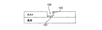
図1aは、基板104によって支持されているホスト層102を示す。
基板は多種多様なタイプの材料で構成されてもよい。
例えば、基板は、プラスチックなどの可撓性材料またはプリント回路基板材料であってもよい。
プラスチックまたは回路基板材料は、剛性または可撓性であるように構成することができる。
あるいは、基板は半導体で形成されてもよい。
1a-1e are diagrams illustrating one method of making a photonic guide element.
This optical waveguide is composed of a hollow core and a highly reflective cladding layer.
This works on the principle of attenuated total reflection.
This is different from conventional optical waveguides that rely on total internal reflection at the critical angle formed between the core and cladding of the waveguide.
FIG. 1 a shows the
The substrate may be composed of a wide variety of types of materials.
For example, the substrate may be a flexible material such as plastic or a printed circuit board material.
The plastic or circuit board material can be configured to be rigid or flexible.
Alternatively, the substrate may be formed of a semiconductor.
ホスト層102は基板材料の上に形成することができる。
ホスト層はまた、標準的なリソグラフィプロセスを使用して処理することができる、ポリマーまたは半導体材料などのタイプの可撓性材料であってもよい。
図1bに示されるように、チャネル106をホスト層に形成することができる。
例えば、ドライエッチングプロセスを使用してチャネルが形成されてもよい。
あるいは、鋳造またはスタンピングプロセスが使用されてもよい。
チャネルの形状は、長方形、正方形、円形、または光を効率的に伝送するために使用される他の何らかの幾何学形状とすることができる。
チャネルの高さ105および/または幅107は、フォトニックガイド素子内に向き付けられる光の波長よりも大幅に大きいことが可能である。
例えば、高さまたは幅は光の波長以上の50倍から100倍以上であってもよい。
The
The host layer may also be a type of flexible material, such as a polymer or semiconductor material, that can be processed using standard lithographic processes.
As shown in FIG. 1b, a
For example, the channel may be formed using a dry etching process.
Alternatively, a casting or stamping process may be used.
The shape of the channel can be rectangular, square, circular, or some other geometric shape used to efficiently transmit light.
The
For example, the height or width may be 50 times to 100 times or more of the wavelength of light.
フォトニックガイド素子内での光の散乱を容易に低減するため、チャネルの壁を平滑化して粗さを低減または排除することができる。
理想的には、壁に沿ったいかなる突出した形体も、光の波長よりも小さいものであるべきである。
チャネルの壁は熱リフロープロセスを使用して平滑化することができる。
このプロセスは、チャネルのエッチングまたはスタンピングによって残った不規則な粗い形体を大幅に低減もしくは排除することができる温度まで、ホストおよび基板材料を加熱することを伴う。
熱リフロープロセスが最適である温度は、ホスト102層および基板104層を形成するのに使用される材料のタイプに依存する。
別の可能性は、側壁の酸化と、それに続く酸化によって形成された酸化物のエッチングである。
In order to easily reduce light scattering within the photonic guide element, the channel walls can be smoothed to reduce or eliminate roughness.
Ideally, any protruding features along the wall should be smaller than the wavelength of light.
The channel walls can be smoothed using a thermal reflow process.
This process involves heating the host and substrate materials to a temperature that can significantly reduce or eliminate the irregular rough features left by channel etching or stamping.
The temperature at which the thermal reflow process is optimal depends on the type of material used to form the
Another possibility is the etching of oxides formed by side wall oxidation followed by oxidation.
チャネル内の反射率を増加させるため、クラッド層108(図1c)が、ホスト層102のチャネル106の内部を覆うために付加されてもよい。
クラッドは、理解されるように、電気めっき、無電解めっき、スパッタリング、または類似のプロセスを使用して形成することができる。
ホスト材料102が、ポリマーまたは低い融点を有する他の材料を含む場合、クラッドは、電気めっき、無電解めっき、スパッタリング、または熱蒸発などの低温プロセスを使用して適用されてもよい。
To increase reflectivity in the channel, a cladding layer 108 (FIG. 1c) may be added to cover the interior of the
The clad can be formed using electroplating, electroless plating, sputtering, or similar processes, as will be appreciated.
If the
クラッド108は、金属、誘電体、またはコヒーレント光の波長において実質的に反射性である他の材料の1つもしくは複数の層で構成することができる。
金属はそれらの反射率に基づいて選択することができる。
高反射性のクラッド層がチャネルを覆うことが望ましい。
例えば、クラッド層は、銀、金、アルミニウム、プラチナ、銅、または高反射性層を形成することができる他の何らかの金属もしくは合金を使用して形成されてもよい。
ホスト材料102に対するクラッド法金属の接着を助けるため、チタンなどの接着層も使用されてもよい。
クラッド層はまた、蒸着プロセス中に生じることがある反射性層の粗い異常を平滑化するため、熱リフローまたは類似のプロセスを施されてもよい。
平滑な鏡面仕上げをもたらすため、電解研磨も使用されてもよい。
The
Metals can be selected based on their reflectivity.
It is desirable that a highly reflective cladding layer covers the channel.
For example, the cladding layer may be formed using silver, gold, aluminum, platinum, copper, or some other metal or alloy that can form a highly reflective layer.
To help adhere the clad metal to the
The cladding layer may also be subjected to thermal reflow or a similar process to smooth out rough irregularities in the reflective layer that may occur during the deposition process.
Electropolishing may also be used to provide a smooth mirror finish.
フォトニックガイド素子が保護されないと、クラッド層108は時間の経過とともに酸化することがある。
反射性コーティングの酸化はその反射率を大幅に低減する可能性がある。
クラッド層の反射率の劣化を低減または排除するため、保護層110をクラッド層の上に形成してシーラントとして作用させることができる。
保護層は、コヒーレント光の波長においてほぼ透明な材料を含むことができる。
例えば、保護層は、反射性コーティングの上に気密接合を形成することができる、二酸化シリコンまたは他の何らかの材料で形成することができる。
さらに、保護層の厚さおよび指数は、損失がより大きい金属層から光ビームを分離することによって、導波路内の伝搬損失をさらに低減するように選択される。
If the photonic guide element is not protected, the
Oxidation of the reflective coating can significantly reduce its reflectivity.
In order to reduce or eliminate the deterioration of the reflectivity of the clad layer, the
The protective layer can include a material that is substantially transparent at the wavelength of the coherent light.
For example, the protective layer can be formed of silicon dioxide or some other material that can form a hermetic bond over the reflective coating.
Further, the thickness and index of the protective layer is selected to further reduce the propagation loss in the waveguide by separating the light beam from the more lossy metal layer.
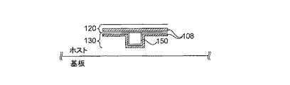
図1dに示されるように、チャネル106、クラッド層108、および保護層110は、フォトニックガイド素子のベース部分130を形成することができる。
蓋部分120は、蓋部分上の反射性コーティングを酸化から保護するように構成された、クラッド層124および保護層126と層状にされたカバー材料122で形成することができる。
クラッド層および保護層は、ベース部分において前述したのと同じ材料を使用して形成することができる。
あるいは、蓋部分の所望の性質に基づいて異なる材料が使用されてもよい。
As shown in FIG. 1d, the
The
The clad layer and the protective layer can be formed using the same material as described above in the base portion.
Alternatively, different materials may be used based on the desired properties of the lid portion.
カバー材料は、反射性コーティングおよび保護層を受け入れるように構成された材料で形成することができる。
フォトニックガイド素子を可撓性にすることができる可撓性材料が選択されてもよい。
例えば、フォトニックガイド素子は、電子素子または光学素子を相互接続するのに使用することができるリボンケーブルとして形成されてもよい。
The cover material can be formed of a material configured to receive the reflective coating and the protective layer.
A flexible material that can make the photonic guide element flexible may be selected.
For example, the photonic guide element may be formed as a ribbon cable that can be used to interconnect electronic or optical elements.
蓋部分120が形成された後、図1eに示されるように、蓋部分をベース部分130に積層または接合することができる。
蓋部分がベース部分に接合されると、大コア(large core)中空導波路150が形成される。
大コア中空導波路は、中空導波路の内部を覆うクラッド層108を有する。
クラッド層によって、光を金属コーティングの表面から反射させて、光が導波路を介して向き付けられるときの減衰を低減することが可能になる。
After the
When the lid portion is joined to the base portion, a large core
The large core hollow waveguide has a
The cladding layer allows light to be reflected from the surface of the metal coating to reduce attenuation when the light is directed through the waveguide.
大コア中空導波路を介して光ビームを伝搬させる際の1つの課題は、特にチップ間通信において、導波路が使用する空間の量である。
一般的な大コア中空導波路は、高さおよび幅がそれぞれ約150ミクロンの断面積を有することがある。
チップサイズが縮小されるにつれて、回路カード上で大コア中空導波路によって使用される面積は相当な大きさになり得る。
それに加えて、図1eの例に示される導波路などの中空金属導波路において、特定の偏光を維持することは困難な場合がある。
多くのタイプの光学チップ部品は、特定の偏光を使用するように設計されている。
導波路を通過する間に生じる偏光の何らかの実質的な変化は、チップ部品における相当量の光学損失をもたらす場合がある。
One challenge in propagating a light beam through a large core hollow waveguide is the amount of space used by the waveguide, especially in chip-to-chip communication.
A typical large core hollow waveguide may have a cross-sectional area of about 150 microns in height and width each.
As the chip size is reduced, the area used by the large core hollow waveguide on the circuit card can become substantial.
In addition, it may be difficult to maintain a specific polarization in a hollow metal waveguide, such as the waveguide shown in the example of FIG. 1e.
Many types of optical chip components are designed to use specific polarizations.
Any substantial change in polarization that occurs while passing through the waveguide may result in a significant amount of optical loss in the chip component.
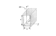
本発明の一実施形態によれば、図2の例示的実施形態に示されるような大コア中空導波路は、特定の偏光状態を維持するように設計することができる。
一実施形態では、光ビームの特定の偏光状態は、光波の偏光に対する中空金属導波路の第1の寸法(dimension)(a)と第2の寸法(b)とのアスペクト比を制御することによって維持することができる。
電磁波の伝搬の原理を簡単に概観することで、この原理を理解する助けとなり得る。
According to one embodiment of the present invention, a large core hollow waveguide as shown in the exemplary embodiment of FIG. 2 can be designed to maintain a particular polarization state.
In one embodiment, the specific polarization state of the light beam is controlled by controlling the aspect ratio of the first dimension (a) and the second dimension (b) of the hollow metal waveguide to the polarization of the light wave. Can be maintained.
A brief overview of the principles of electromagnetic wave propagation can help understand this principle.
マクスウェルの方程式によって理解できるように、電磁波は電界Eおよび磁界Hを伴って空気中を伝搬する。
電界および磁界は互いに直交し、それら両方が一般に伝搬方向に対して直交する。
電界の方向は一般的に「偏波」と称される。
例えば、電界がx軸で偏波すると言われる場合、磁界はx軸に直交するy軸に向き付けられる。
これはEXおよびHYと表すことができる。
次に、電磁波はz軸に沿って伝搬することができる。
電磁波はモードの形で伝搬することもできる。
モードはpおよびqと表すことができ、それぞれx軸およびy軸に沿ったモードプロファイルにおけるローブの数を表す。
これにより、電界がx軸にある場合にz軸に沿って移動する光波がEX pqおよびHY pqと表される。
最低次モードはp=1およびq=1、すなわちEX 11およびHY 11である。
電界がY次元にある状態で移動する光波の場合、モードはEY pqおよびHX pqと表される。
As can be understood from Maxwell's equations, electromagnetic waves propagate in the air with an electric field E and a magnetic field H.
The electric and magnetic fields are orthogonal to each other, and both are generally orthogonal to the propagation direction.
The direction of the electric field is generally referred to as “polarization”.
For example, if the electric field is said to be polarized on the x axis, the magnetic field is directed to the y axis, which is orthogonal to the x axis.
This can be expressed as E X and H Y.
The electromagnetic wave can then propagate along the z-axis.
Electromagnetic waves can also propagate in the form of modes.
Modes can be expressed as p and q, representing the number of lobes in the mode profile along the x-axis and y-axis, respectively.
Thereby, when the electric field is on the x-axis, the light waves that move along the z-axis are expressed as E X pq and H Y pq .
The lowest order modes are p = 1 and q = 1, ie E X 11 and H Y 11 .
For light waves that move with the electric field in the Y dimension, the modes are denoted E Y pq and H X pq .
大コア中空導波路内の電界の伝搬損失を導き出すことができる。
空のコア(ncore=1)では、電界がx次元およびy次元にある場合の損失定数αは次式を有する。
The propagation loss of the electric field in the large core hollow waveguide can be derived.
For an empty core (n core = 1), the loss constant α when the electric field is in the x and y dimensions has the following equation:

式中、λは光の波長、nはクラッド材料の複素屈折率、pおよびqは電界のモード、aおよびbはそれぞれx方向およびy方向の導波路の寸法である。
第1項は(a)の分だけ分離された垂直壁によって引き起こされる伝搬損失を表し、第2項は(b)の分だけ分離された水平壁によって引き起こされる伝搬損失を表す。
αの次元の数は長さの逆数であることに留意されたい。
dB/長さ単位の伝搬損失はdB/長さ=8.686αによって与えられる。
Where λ is the wavelength of light, n is the complex refractive index of the cladding material, p and q are the modes of the electric field, and a and b are the dimensions of the waveguides in the x and y directions, respectively.
The first term represents the propagation loss caused by the vertical wall separated by (a), and the second term represents the propagation loss caused by the horizontal wall separated by (b).
Note that the number of dimensions of α is the reciprocal of the length.
The propagation loss in dB / length is given by dB / length = 8.666α.
分子におけるn2値は1つの次元のみと関連しているため、その次元の損失は著しく多い可能性がある。
例えば、銀のクラッドが使用される場合、λ=850nmの波長におけるn2の値は約32である。
金または銅のクラッドが使用されると、同じ波長におけるn2の値はそれぞれ約31および29である。
a=b(正方形の導波路)であり、かつEYモードのとき、上述の式の2番目から推定されるように、垂直(即ち、電界に対して平行)壁が引き起こす損失は水平(即ち、電界に対して垂直)壁の約30分の1である。
EXモードが使用される場合、水平壁が引き起こす損失は垂直壁の約30分の1である。
したがって、正方形の導波路の場合、電界と平行な壁が引き起こす伝搬損失は電界に垂直な壁よりも大幅に少ない。
Since n 2 values in a numerator are associated with only one dimension, the loss of that dimension can be significant.
For example, if a silver cladding is used, the value of n 2 at a wavelength of λ = 850 nm is about 32.
If gold or copper cladding is used, the value of n 2 at the same wavelength is about 31 and 29, respectively.
When a = b (square waveguide) and in EY mode, the loss caused by the vertical (ie parallel to the electric field) wall is horizontal (ie , Perpendicular to the electric field) about one-third of the wall.
If E X mode is used, losses caused by the horizontal walls is 1 to about 30 minutes of the vertical walls.
Thus, in the case of a square waveguide, the propagation loss caused by the wall parallel to the electric field is significantly less than the wall perpendicular to the electric field.
結果として、損失は導波路パラメータの変化に対して異なる感度を有する。
即ち、垂直に偏波されたEYモードが使用されるとき、垂直壁間の距離(パラメータa)の変化に伴う損失量の変化は比較的少ない。
しかし、損失は水平壁間の距離(パラメータb)に伴ってはるかに大幅に(約30倍の率で)変化する。
したがって、導波路寸法(a)を大幅に低減させ、その結果として生じる、導波路寸法(b)のわずかな増加に伴う損失量の増加を補償することができる。
低減された高さまたは幅は導波路が占める面積を減少させるので、偏光を用いた操作によって原理上はチップ上の面積の相当量を節約することができる。
As a result, the loss has a different sensitivity to changes in the waveguide parameters.
That is, when the E Y mode is vertically polarized wave is used, the change in loss due to the change in the distance of the vertical walls (parameter a) is relatively small.
However, the loss varies much more (at a rate of about 30 times) with the distance between the horizontal walls (parameter b).
Therefore, the waveguide dimension (a) can be greatly reduced, and the resulting increase in loss accompanying a slight increase in the waveguide dimension (b) can be compensated.
Since the reduced height or width reduces the area occupied by the waveguide, operation with polarized light can in principle save a considerable amount of area on the chip.
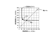
例えば、図3は、ミクロン単位で測定した幅(a)および高さ(b)を有する導波路のサイズに対する一定損失のラインを示すグラフである。
この例における一定損失のラインは0.0015dB/cmの値である。
正方形の導波路302がグラフ上にマークされて、幅および高さ150ミクロンを示している。
大幅に低減された幅(〜65ミクロン)と比較的小さな高さの増加(〜170ミクロン)を有する長方形の導波路304は、正方形の導波路とほぼ同じ伝搬損失を有することができる。
長方形の導波路の断面積は、正方形の導波路の場合の22,500平方ミクロンから長方形の導波路の場合の11,050平方ミクロンまで低減されている。
したがって、長方形の導波路の面積は正方形の導波路の2分の1未満であり、正方形の導波路を伝搬される光とほぼ類似の損失量を有する。
For example, FIG. 3 is a graph showing a line of constant loss versus the size of a waveguide having width (a) and height (b) measured in microns.
The constant loss line in this example has a value of 0.0015 dB / cm.
A
A
The cross-sectional area of the rectangular waveguide is reduced from 22,500 square microns for the square waveguide to 11,050 square microns for the rectangular waveguide.
Accordingly, the area of the rectangular waveguide is less than half that of the square waveguide, and the loss amount is almost similar to that of light propagated through the square waveguide.
一般に、EX pqおよびEY pqモードタイプ両方の損失は同じスケーリング則に従う。
損失は光の波長の二乗に比例して増加し、導波路寸法の三乗に反比例して低減される(伝搬損失)〜(λ2/(導波路寸法)3)。
しかし、損失に対する第1の導波路寸法および第2の導波路寸法(幅および高さ)の寄与は不均等である。
所与のモードタイプ(固定の偏波)の場合、電界と平行な壁による損失は比較的小さいが、電界に垂直な壁による損失は比較的大きい。
上述したように、2つの損失タイプの比はn2 cladの絶対値付近である。
したがって、電界と平行な壁は比較的低損失の壁と見なすことができ、電界に垂直な壁は比較的高損失の壁と見なすことができる。
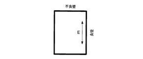
このことは、電界Eを有する大コア中空導波路を示す図4に概略的に示される。
電界と平行な導波路の壁の損失は電界に垂直な壁よりも大幅に低い。
したがって、長方形の導波路を使用すると、損失を最小限に抑えるため、電界が導波路の長壁と平行な方向にある状態で電磁波を伝搬させることができる。
In general, the losses for both E X pq and E Y pq mode types follow the same scaling law.
The loss increases in proportion to the square of the wavelength of light and is reduced in inverse proportion to the cube of the waveguide dimension (propagation loss) to (λ 2 / (waveguide dimension) 3 ).
However, the contributions of the first and second waveguide dimensions (width and height) to the loss are unequal.
For a given mode type (fixed polarization), the loss due to walls parallel to the electric field is relatively small, but the loss due to walls perpendicular to the electric field is relatively large.
As described above, the ratio of the two loss types is near the absolute value of n 2 clad .
Therefore, a wall parallel to the electric field can be regarded as a relatively low-loss wall, and a wall perpendicular to the electric field can be regarded as a relatively high-loss wall.
This is shown schematically in FIG. 4 which shows a large core hollow waveguide with an electric field E.
The loss of the waveguide wall parallel to the electric field is significantly lower than the wall perpendicular to the electric field.
Therefore, when a rectangular waveguide is used, electromagnetic waves can be propagated in a state where the electric field is in a direction parallel to the long wall of the waveguide in order to minimize loss.
赤外光または可視光のビームなど、長方形の大コア中空導波路内を伝搬される電磁波は、電界の垂直方向の損失が平行方向に対して大幅に大きくなる。
これによって、ビームが導波路を移動するにつれて平行方向で大きく偏光される。
実質的に不規則に偏光されるビームを長方形の大コア中空導波路を介して伝送することによって、導波路の長壁に垂直なビームにおける電磁波の損失が比較的高くなる。
既に長壁に平行に偏光されているビームは、比較的低い損失量で導波路を移動する際にその偏光が維持される。
これによって、特定のタイプの偏光に依存する光学部品を通信アーキテクチャに使用することが可能になる。
An electromagnetic wave propagating through a rectangular large-core hollow waveguide, such as an infrared light beam or a visible light beam, has a large loss in the vertical direction of the electric field with respect to the parallel direction.
This greatly polarizes in the parallel direction as the beam moves through the waveguide.
By transmitting a substantially randomly polarized beam through a rectangular large core hollow waveguide, the loss of electromagnetic waves in the beam perpendicular to the long wall of the waveguide is relatively high.
A beam that is already polarized parallel to the long wall maintains its polarization as it travels through the waveguide with a relatively low loss.
This allows optical components that depend on a particular type of polarization to be used in the communication architecture.
偏光および非対称の長方形の導波路を用いた操作によってさらなる利益を付加することができる。
長方形の導波路の一次元は、全体の吸収損失に影響を及ぼすことなく著しく低減させることができる。
これによって、コンピュータ回路ボードおよび/またはコンピュータチップ上の面積の相当量を節約することができる。
導波路の幅を低減し、その高さを増加させることによって、回路基板で使用される全体面積が低減され、それによってより小さな回路基板を使用することが可能になる。
Additional benefits can be added by manipulating with polarized and asymmetric rectangular waveguides.
One dimension of the rectangular waveguide can be significantly reduced without affecting the overall absorption loss.
This can save a considerable amount of area on the computer circuit board and / or computer chip.
By reducing the width of the waveguide and increasing its height, the overall area used on the circuit board is reduced, thereby allowing the use of smaller circuit boards.
伝搬損失は平行な壁と垂直の壁とで異なるので、異なるタイプの誘電体コーティングを壁に使用することが有益な場合がある。
例えば、第1のタイプの誘電体コーティングは、導波路を介して伝搬される光の電界と平行な導波路壁に使用されてもよい。
第2のタイプの誘電体コーティングは、電界に垂直な壁に使用することができる。
誘電体コーティングによって、電界を金属クラッドに侵入させて所望に応じて侵入を最大化あるいは最小化することを可能にする、2つの波の間の付加的なインターフェースがもたらされる。
誘電体コーティングの最適な厚さは、導波路を伝搬する光波のs偏光およびp偏光の反射率を最大限にするように選択することができる。
Since propagation losses are different between parallel and vertical walls, it may be beneficial to use different types of dielectric coatings on the walls.
For example, a first type of dielectric coating may be used on a waveguide wall parallel to the electric field of light propagating through the waveguide.
A second type of dielectric coating can be used on the walls perpendicular to the electric field.
The dielectric coating provides an additional interface between the two waves that allows the electric field to penetrate the metal cladding and maximize or minimize penetration as desired.
The optimal thickness of the dielectric coating can be selected to maximize the reflectivity of the s-polarized light and the p-polarized light traveling through the waveguide.
堅牢な通信アーキテクチャを構築するためには、直線セグメントにおける低い伝搬損失は一般的に不十分である。
チップと基板との間で光学信号の経路を定める目的で、湾曲した導波路セグメントを介して所望の伝送を得ることが必要なことがある。
これらの湾曲したセグメントを使用して、導波路に屈曲を形成することができる。
曲率半径Rを有する大コア中空導波路500の例示的実施形態が図5に示される。
直線の導波路と同様に、湾曲した導波路は、第1の寸法504とそれよりも大幅に大きい第2の寸法506を含むことができる。
導波路の曲率半径Rと伝搬されるビームの波長λとの比が1よりもはるかに大きい場合(R/λ>>1)、電界502が屈曲面に対して垂直である光ビームの最低次モードについての伝搬損失の解を、いくつかの近次式を用いて分析的に求めて、次の結果を得ることができる。
In order to build a robust communication architecture, low propagation loss in the straight line segment is generally insufficient.
In order to route the optical signal between the chip and the substrate, it may be necessary to obtain the desired transmission through a curved waveguide segment.
These curved segments can be used to form a bend in the waveguide.
An exemplary embodiment of a large core
Similar to a straight waveguide, a curved waveguide can include a
If the ratio between the radius of curvature R of the waveguide and the wavelength λ of the propagated beam is much greater than 1 (R / λ >> 1), the lowest order of the light beam in which the
例えば、銀のクラッドを有し、波長850nmの光ビームを伝搬する大コア中空導波路を使用すると(nclad=0.152+i×5.678)、損失は次式のとおりである。 For example, when a large core hollow waveguide having a silver cladding and propagating a light beam having a wavelength of 850 nm is used (n clad = 0.152 + i × 5.678), the loss is as follows.
式中、半径Rはセンチメートル単位で測定される。
したがって、損失αは単位長さ当たりの損失であり、屈曲半径に反比例する。
ほとんどの幾何学形状の場合、屈曲の線形長さは半径に比例する。
その結果、大コア中空金属導波路において、1つの屈曲当たりの合計損失は屈曲半径にはほぼ依存しない。
銀コーティングした導波路におけるEZ 11モードでは、電界が屈曲面に垂直な場合、90°の屈曲を通過した後の合計損失は約0.06dBである。
図5の中の例示的図面では、屈曲面は湾曲した導波路の床507(または天井)と平行な面である。
したがって、偏光波の電界502は湾曲した導波路の床および天井に垂直である。
Where the radius R is measured in centimeters.
Therefore, the loss α is a loss per unit length and is inversely proportional to the bending radius.
For most geometric shapes, the linear length of bending is proportional to the radius.
As a result, in a large core hollow metal waveguide, the total loss per bend is almost independent of the bend radius.
In the E Z 11 mode in a silver coated waveguide, the total loss after passing through a 90 ° bend is approximately 0.06 dB when the electric field is perpendicular to the bend plane.
In the exemplary drawing in FIG. 5, the curved surface is a plane parallel to the curved waveguide floor 507 (or ceiling).
Thus, the
Erモードでは、電界は動径座標に沿っている。
換言すれば、屈曲面と平行(床507に垂直)である。
電界が屈曲面と平行である光ビームの最低次モードについての伝搬損失の解を、いくつかの近次式を用いて分析的に求めて、次の結果を得ることができる。
In the Er mode, the electric field is along the radial coordinate.
In other words, it is parallel to the bent surface (perpendicular to the floor 507).
The solution of the propagation loss for the lowest order mode of the light beam whose electric field is parallel to the curved surface can be analytically determined using several near-order equations to obtain the following results.
電界が屈曲面と平行であるこの損失係数は、概して、EZモードの場合よりも大きいn2 cladの因数である。
したがって、直線の導波路を光ビームが伝搬する場合と同様に、電界が導波路壁(この場合、伝搬損失の大半に関与する外側の湾曲壁)に垂直である伝搬における損失は、電界が壁と平行である伝搬よりもはるかに大きくなる。
850nmの銀のクラッドの場合、次式のとおりである。
This loss factor, where the electric field is parallel to the bent surface, is generally a factor of n 2 clad that is greater than in the EZ mode.
Thus, as in the case of a light beam propagating through a straight waveguide, loss in propagation where the electric field is perpendicular to the waveguide wall (in this case, the outer curved wall responsible for most of the propagation loss) Much larger than the propagation that is parallel to.
In the case of a 850 nm silver clad,
式中、半径Rはセンチメートル単位で測定される。
90°の屈曲の合計吸収損失は約2.1dBである。
これらの損失は理論下限値であることに留意されたい。
実際には、側壁の散乱および他の効果と関連する付加的な損失もある。
しかし、全体損失は一般的にこれらの理論値以上である。
Where the radius R is measured in centimeters.
The total absorption loss for a 90 ° bend is about 2.1 dB.
Note that these losses are lower theoretical limits.
In practice, there are also additional losses associated with side wall scattering and other effects.
However, the overall loss is generally above these theoretical values.
したがって、大コア中空金属化導波路に90°の屈曲を5つ含む通信アーキテクチャの場合、電界が屈曲面に垂直である偏光ビームは約0.06×5=0.3dBの損失を有する。
電界が屈曲面と平行である偏光ビームの場合、損失は約2.1×5=10.5dBである。
後者の損失量は、一般に、低出力レーザーまたは発光ダイオードを使用して通信するチップ間通信において保持することができない。
したがって、大コア中空導波路を介して伝送される偏光スクランブルビームによって、屈曲面と平行な電界が大幅に損失した光ビームがもたらされる。
したがって、屈曲を有する大コア中空導波路を使用するとき、図5に示されるように、屈曲面にほぼ垂直な偏光を使用して損失を制限することが有益である。
円筒座標φ、r、およびzを使用して、円筒座標系の軸線が示される。
Thus, for a communication architecture that includes five 90 ° bends in a large core hollow metallized waveguide, a polarized beam whose electric field is perpendicular to the bend has a loss of about 0.06 × 5 = 0.3 dB.
For a polarized beam whose electric field is parallel to the curved surface, the loss is about 2.1 × 5 = 10.5 dB.
The latter amount of loss generally cannot be preserved in chip-to-chip communications that communicate using low power lasers or light emitting diodes.
Therefore, the polarization scrambled beam transmitted through the large core hollow waveguide provides a light beam in which the electric field parallel to the bent surface is greatly lost.
Therefore, when using a large core hollow waveguide with a bend, it is beneficial to limit the loss using polarized light approximately perpendicular to the bend as shown in FIG.
The cylindrical coordinates φ, r, and z are used to indicate the axis of the cylindrical coordinate system.
導波路の屈曲を介する一般的な伝搬損失と直線の導波路における一般的な伝搬損失との比は、およそ、(導波路幅)3/(波長)2/(曲率半径)である。
導波路幅約100マイクロメートル、波長約1マイクロメートル、および半径約10,000マイクロメートル(1cm)の場合、比は約100である。
したがって、屈曲損失は直線損失の約2倍程度である。
したがって、大コア中空金属化導波路の屈曲の数を制限することで、通信アーキテクチャの損失量は相当量減少する。
しかし、湾曲が必要なとき、光ビームが導波路の屈曲面に垂直な電界偏波を有する長方形の導波路を使用することで、損失を最小限に抑えることができる。
The ratio of typical propagation loss through waveguide bending to typical propagation loss in a straight waveguide is approximately (waveguide width) 3 / (wavelength) 2 / (curvature radius).
For a waveguide width of about 100 micrometers, a wavelength of about 1 micrometer, and a radius of about 10,000 micrometers (1 cm), the ratio is about 100.
Therefore, the bending loss is about twice the linear loss.
Therefore, by limiting the number of bends in the large core hollow metallized waveguide, the amount of communication architecture loss is significantly reduced.
However, when bending is required, the loss can be minimized by using a rectangular waveguide in which the light beam has an electric field polarization perpendicular to the bending surface of the waveguide.
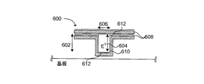
長方形の導波路で利用可能なより低い損失および偏光の維持を利用するため、図6に示されるように、非常に長い第1の次元(dimension)602を有する大コア中空金属化導波路600が形成されてもよい。
第2の次元606は第1の次元に対して相対的に垂直であることができる。
ほぼ直線の導波路の場合、偏光を使用して、電界EY604が導波路の細長い次元602とほぼ平行である偏光ビームを伝送することができる。
湾曲した導波路の場合、電界が屈曲面に垂直であるEZ偏光ビームを湾曲した導波路を介して向き付けることができる。
In order to take advantage of the lower loss and polarization maintenance available with rectangular waveguides, a large core hollow metallized
The
For a substantially straight waveguide, polarization can be used to transmit a polarized beam whose
In the case of a curved waveguide, an EZ polarized beam whose electric field is perpendicular to the bending surface can be directed through the curved waveguide.
導波路600の第1および第2の次元は、導波路内で光が移動する方向に直交することができる。
電界が第1の次元とほぼ平行な光波が、第2の次元とほぼ平行な電界を有する光波よりも大幅に少ない損失で導波路を伝搬できるようにするため、第1の次元602に沿った導波路壁の長さは、第2の次元606に沿った導波路壁の長さよりも大幅に大きくすることが可能である。
例えば、1つの例示的実施形態では、導波路の第1の次元の細長い壁は約170マイクロメートルの長さを有することができる。
第2の次元の壁は約65マイクロメートルの長さを有することができる。
この例では、導波路を介して移動する光ビームの伝搬損失は、導波路の第1の次元の三乗の逆数に応じて減少する。
The first and second dimensions of the
Along the
For example, in one exemplary embodiment, the first dimension elongated wall of the waveguide can have a length of about 170 micrometers.
The second dimension wall can have a length of about 65 micrometers.
In this example, the propagation loss of the light beam traveling through the waveguide decreases with the inverse of the cube of the first dimension of the waveguide.
電界と平行な壁の誘電体コーティング610は、選択された厚さでクラッド608の上に付加することができる。
誘電体コーティング612も、第2の次元606に対する壁上で、選択された厚さでクラッドの上に付加することができる。
クラッドの厚さは、電磁波がクラッドと相互作用する際の損失を最小限に抑えるように選択することができる。
A
A
The thickness of the cladding can be selected to minimize losses when electromagnetic waves interact with the cladding.
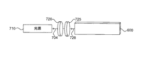
図7aは、長方形の大コア金属化中空導波路600を含むフォトニックガイド素子のブロック図を示す。
フォトニックガイド素子は光源710に結合することができる。
光源は、発光ダイオード、レーザー、または光ビーム704を放射するように動作可能な他のタイプの発光素子であることができる。
単一モードレーザーは多重モードレーザーよりも大幅に高価な場合がある。
したがって、多重モードレーザーを光源として使用することで、システム全体のコストを大幅に低減することができる。
しかし、多重モードレーザーを使用することの1つの欠点は、レーザー光の相当な部分が、光が放射される方向に対してかなり大きな角度でレーザーから放射される場合がある点である。
レーザー光線の高次モードは、レーザーから光が放射されるよりも大きな角度に相当する。
大角度で放射される光は、大コア中空導波路600内でより多数回反射することになる。
反射の数が多いほど、導波路内でより多量の光が減衰する。
したがって、高次モードは導波路内で大幅に減衰することがある。
FIG. 7 a shows a block diagram of a photonic guide element that includes a rectangular large core metallized
A photonic guide element can be coupled to the
The light source can be a light emitting diode, a laser, or other type of light emitting element operable to emit a
Single mode lasers can be significantly more expensive than multimode lasers.
Therefore, the cost of the entire system can be significantly reduced by using a multimode laser as the light source.
However, one drawback of using a multimode laser is that a significant portion of the laser light may be emitted from the laser at a fairly large angle with respect to the direction in which the light is emitted.
The higher order mode of the laser beam corresponds to a larger angle than the light emitted from the laser.
Light emitted at a large angle will be reflected more times within the large core
The greater the number of reflections, the more light is attenuated in the waveguide.
Therefore, higher order modes can be significantly attenuated in the waveguide.
反射面を有する中空導波路は固体導波路とは異なるように動作する。
中空導波路は、光ファイバーなどの固体導波路で一般的に起こるように、全反射ではなく反射層(1つまたは複数)からの反射によって光をガイドする。
理解されるように、中空導波路内の光は、全反射に必要な角度よりも小さい角度で反射されることがある。
A hollow waveguide with a reflective surface operates differently than a solid waveguide.
Hollow waveguides guide light by reflection from the reflective layer (s) rather than total reflection, as typically occurs in solid state waveguides such as optical fibers.
As will be appreciated, the light in the hollow waveguide may be reflected at an angle less than that required for total reflection.
光源710から放射される高次モードの減衰を克服するため、光源からの光ビーム704の経路内にコリメータ720を配置することができる。
一実施形態では、光源は多重モードレーザーであってもよい。
多重モード光を放射するように動作可能な他のタイプの光エミッタも使用されてもよい。
コリメータは、反射防止コーティングを有するボールレンズなどのコリメーティングレンズであることができる。
コリメータは、光源から放射された多重モードビームが大コア中空導波路600に入る前に平行ビームへとコリメートするように構成される。
コリメータは、発生するほぼあらゆる反射が、一般的に導波路壁に対して比較的浅い角度になるようにし、それによって導波路内の反射の数を最小限に抑え、したがって、中空導波路内の光の減衰を低減する。
その結果、中空導波路内で伝搬する低損失モードは非常に小さい開口数を有する。
この性質によって、余分な損失をほとんど伴わずに光学スプリッタをこれらの導波路に挿入することができる。
A
In one embodiment, the light source may be a multimode laser.
Other types of light emitters operable to emit multimode light may also be used.
The collimator can be a collimating lens such as a ball lens having an anti-reflective coating.
The collimator is configured to collimate the multimode beam emitted from the light source into a collimated beam before entering the large core
The collimator ensures that almost any reflection that occurs is generally at a relatively shallow angle with respect to the waveguide wall, thereby minimizing the number of reflections in the waveguide, and thus in the hollow waveguide. Reduce light attenuation.
As a result, the low loss mode propagating in the hollow waveguide has a very small numerical aperture.
This property allows optical splitters to be inserted into these waveguides with little extra loss.
光ビーム704を偏光するのに偏光子725を使用することができる。
例えば、偏光子およびコリメータ720を使用して、長方形の導波路の長い寸法と平行な偏光EYを有する、偏光された多重モード光ビーム728を形成することができる。
波長850nmのビームを、0.001dB/cm程度の損失で、反射性コーティングを有する長方形の大コア導波路を介して伝送することができる。
コリメーティングレンズを使用して、多重モードコヒーレント光が大コア導波路を通るように向き付けることで、フォトニックガイド素子全体のコストを大幅に低減することもできる。
多重モードレーザーはそれらの単一モードの等価物よりも大幅に安価である。
A
For example, using a polarizer and a
A beam with a wavelength of 850 nm can be transmitted through a rectangular large core waveguide with a reflective coating with a loss of about 0.001 dB / cm.
By using a collimating lens and directing multimode coherent light through a large core waveguide, the cost of the entire photonic guide element can be significantly reduced.
Multimode lasers are significantly less expensive than their single mode equivalents.
したがって、導波路内に向き付けられた多重モードコヒーレント光をコリメートするように構成されたコリメータに内部反射面が結合された、長方形の大コア中空金属化導波路を備えるフォトニックガイド素子は、部品を1つまたは複数のプリント回路基板上で相互接続するための比較的安価で低損失の手段としての役割を果たすことができる。
ガイド素子が低損失であることによって、それら素子を、電子回路類を光学的に相互接続するなど、より一般的に汎用製品に使用されるものにすることができる。
Thus, a photonic guide element comprising a rectangular large core hollow metallized waveguide with an internal reflective surface coupled to a collimator configured to collimate multimode coherent light directed into the waveguide is a component. Can serve as a relatively inexpensive and low-loss means for interconnecting on one or more printed circuit boards.
The low loss of the guide elements can make them more commonly used in general purpose products, such as optically interconnecting electronic circuitry.
電子回路類は、回路群から伝送される電気信号が光学信号に、またはその逆に変換される電気回路類を含むことができる。
変換の必要なく光学信号を使用して直接通信することができる、光学回路類も使用することができる。
光学回路類は、所望のタイプの偏光を提供するように設計された光学部品を含んでもよい。
長方形の大コア中空金属化導波路を使用して、ビームが回路基板上の1つの部品から別の部品へと向き付けられる際に所望の偏光を維持することができる。
電子および光学回路類は単一の回路基板上に収められてもよい。
あるいは、電子および光学回路類は2つ以上の別個の回路基板上に位置してもよく、導波路を使用して基板を相互接続することができる。
傾斜させた半反射面を使用することによって、これらの導波路からの光学信号をタッピングし、向き付けることも比較的簡単である。
従来の導波路は開口数がより大きいため、これは従来の導波路の場合の方がむしろ困難である。
Electronic circuitry can include electrical circuitry in which electrical signals transmitted from a group of circuits are converted to optical signals or vice versa.
Optical circuitry that can communicate directly using optical signals without the need for conversion can also be used.
The optical circuitry may include optical components designed to provide the desired type of polarization.
A rectangular large core hollow metallized waveguide can be used to maintain the desired polarization as the beam is directed from one component to another on the circuit board.
Electronic and optical circuitry may be contained on a single circuit board.
Alternatively, the electronic and optical circuitry may be located on two or more separate circuit boards, and waveguides can be used to interconnect the boards.
By using an inclined semi-reflective surface, it is also relatively easy to tap and direct the optical signals from these waveguides.
This is rather difficult in the case of conventional waveguides because conventional waveguides have a higher numerical aperture.
例えば、図7bは、内部反射面を有する長方形の大コア中空導波路600を示す。
中空導波路は2つの回路基板740を光学的に結合するのに使用される。
上述したように、中空導波路のサイズが比較的大きいことによって、基板間で導波路を相互接続するコストを低減することができる。
導波路内の反射面は損失を低減して、コヒーレント光の低出力信号を、導波路を介して隣接した回路基板に伝送することができる。
回路基板の一方または両方の上に位置する安価な多重モードレーザーまたは他のタイプの発光素子を使用して、光を伝送することができる。
コリメーティングレンズを回路基板の一方または両方に含め、導波路に光学的に結合することができる。
コリメーティングレンズは、複数回の反射によって引き起こされる光の高次モードの損失を低減することができる。
長方形の導波路を使用することによって、損失をさらに低減し、第1の回路基板からの偏光ビームを維持し、第2の回路基板へと通信することができる。
長方形の中空導波路600の相互接続は、製造プロセスにおいて基板間に結合されるように構成されてもよい。
あるいは、中空導波路は、基板の製造後に基板に接続することができるコネクタおよび/またはケーブルとして形成されてもよい。
For example, FIG. 7b shows a rectangular large core
The hollow waveguide is used to optically couple the two
As described above, since the size of the hollow waveguide is relatively large, the cost of interconnecting the waveguides between the substrates can be reduced.
The reflective surface in the waveguide reduces the loss, and a low-power signal of coherent light can be transmitted to the adjacent circuit board through the waveguide.
An inexpensive multimode laser or other type of light emitting element located on one or both of the circuit boards can be used to transmit the light.
A collimating lens can be included on one or both of the circuit boards and optically coupled to the waveguide.
The collimating lens can reduce high-order mode loss of light caused by multiple reflections.
By using a rectangular waveguide, the loss can be further reduced, the polarized beam from the first circuit board can be maintained and communicated to the second circuit board.
The rectangular
Alternatively, the hollow waveguide may be formed as a connector and / or cable that can be connected to the substrate after manufacture of the substrate.
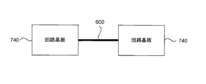
内部反射面を有する中空導波路600は、また、図7cに示されるように、単一の回路基板740上の電子部品745を相互接続するのに使用されてもよい。
上述したように、導波路の長方形の寸法によって、回路基板上で導波路用に使用される面積を低減し、最小限の損失で偏光ビームを通信することができる。
光学または電子部品は、偏光ビームを1つの導波路から別の導波路へと向け直すのに使用してもよい。
あるいは、90°の湾曲部748など、導波路の湾曲部を使用することができる。
一実施形態では、湾曲部は、光の波長よりも大幅に大きい曲線半径を有することができる。
湾曲した導波路を介して伝送される光ビームは、湾曲の面に垂直な方向の電界で偏光して、損失を最小限に抑えることができる。
A
As described above, the rectangular dimensions of the waveguide can reduce the area used for the waveguide on the circuit board and communicate the polarized beam with minimal loss.
Optical or electronic components may be used to redirect the polarized beam from one waveguide to another.
Alternatively, waveguide bends such as 90 °
In one embodiment, the curve may have a curve radius that is significantly greater than the wavelength of light.
A light beam transmitted through a curved waveguide can be polarized with an electric field in a direction perpendicular to the plane of curvature to minimize loss.
長方形の金属化大コア中空導波路はまた、複数の信号を向き付けられるようにするため、アレイ状に形成することができる。
例えば、図8aは、長方形の中空導波路830の一次元のアレイ800を示す。
上述したように、各導波路はクラッド層802を含むことができる。
クラッド層は、酸化を低減するため、保護層804でコーティングすることができる。
あるいは、保護層は、クラッド層における光ビームの吸収を低減するのに使用される誘電体層であってもよい。
導波路のアレイは、基板またはホスト材料808上に構築することができる。
一実施形態では、長方形の導波路のより長い寸法810は、導波路によって使用されるホスト材料上の面積を最小限に抑えるため、基板またはホスト材料から離れる方向に向き付けることができる。
光学信号の偏光モードは、損失を最小限に抑え、かつ導波路を介する偏光モードを維持するように選択することができる。
上述したように、長軸810と平行な電界を有する偏光モードを使用して、損失を最小限に抑え、かつ導波路を介する光学信号の偏光を維持することができる。
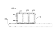
Rectangular metalized large core hollow waveguides can also be formed in an array to allow multiple signals to be directed.
For example, FIG. 8 a shows a one-
As described above, each waveguide can include a
The cladding layer can be coated with a
Alternatively, the protective layer may be a dielectric layer used to reduce light beam absorption in the cladding layer.
An array of waveguides can be built on the substrate or
In one embodiment, the
The polarization mode of the optical signal can be selected to minimize loss and maintain the polarization mode through the waveguide.
As described above, a polarization mode having an electric field parallel to the
図8bは、回路基板に結合された中空導波路830のアレイ800を示す。
回路基板は、アレイの各中空導波路を取り付けることができる基板808(図8a)として作用することができる。
一実施形態では、回路基板は光学バックプレーン825として構成することができる。
上述したように、コリメータを使用して、多重モードコヒーレント光を導波路それぞれに向き付けることができる。
光学スプリッタなどの結合素子822は、ガイドされた多重モードコヒーレント光ビームの少なくとも一部分を、選択された位置で導波路外へと向き付けるように構成することができる。
例えば、図8bに示されるように、結合素子を使用して、中空導波路内のコヒーレント光の少なくとも一部分を、回路基板の面外にある光学的に結合された大コア中空導波路824へと向けなおすことができる。
光学的に結合された導波路はバックプレーンに直交してもよいが、実質的にあらゆる角度が使用されてもよい。
FIG. 8b shows an
The circuit board can act as a substrate 808 (FIG. 8a) to which each hollow waveguide of the array can be attached.
In one embodiment, the circuit board can be configured as an
As described above, a collimator can be used to direct multimode coherent light to each waveguide.
A
For example, as shown in FIG. 8b, a coupling element is used to transfer at least a portion of the coherent light in the hollow waveguide to an optically coupled large core
The optically coupled waveguide may be orthogonal to the backplane, but virtually any angle may be used.
多重モードコヒーレント光を回路基板の面外に向けなおすことによって、ドーターボード820などの複数の回路カードをバックプレーン825に光学的に結合することが可能になる。
コヒーレント光信号上で符号化される高データ率の情報を、バックプレーンから複数のドーターボードへと向けなおすか、または分配することができる。
By redirecting the multimode coherent light out of the plane of the circuit board, a plurality of circuit cards such as the
High data rate information encoded on the coherent optical signal can be redirected or distributed from the backplane to multiple daughter boards.
反射性の内部コーティングを有する長方形の大コア中空導波路によって、高データ率の情報を複数の異なる基板へと伝送することが可能になる。
中空導波路の損失が低いことによって、図8bに示されるように、単一の光学信号の経路を他の複数の導波路内へと定めることが可能になる。
各導波路を介してガイドされる多重モードコヒーレント光ビームは、毎秒数十ギガビット以上の転送率でデータを運ぶことができる。
モードの指数はほぼ一貫しているので、光ビームは本質的に光の速度で伝搬し、結果として伝搬遅延はほぼ最小限になる。
中空導波路によって可能になる光接続によって、チップと回路基板との間のスループットを大幅に増加させるための安価な手段がもたらされる。
長方形の導波路を使用することによって、偏光された信号を維持し、回路基板上の導波路によって使用される面積を低減することが可能になるとともに、光学信号伝搬における大幅に低い損失が維持される。
A rectangular large core hollow waveguide with a reflective inner coating allows high data rate information to be transmitted to multiple different substrates.
The low loss of the hollow waveguide makes it possible to route a single optical signal into other waveguides, as shown in FIG. 8b.
A multimode coherent light beam guided through each waveguide can carry data at a transfer rate of several tens of gigabits per second or more.
Since the mode exponents are almost consistent, the light beam inherently propagates at the speed of light, resulting in nearly minimal propagation delay.
The optical connection made possible by the hollow waveguide provides an inexpensive means to significantly increase the throughput between the chip and the circuit board.
By using a rectangular waveguide, it is possible to maintain a polarized signal, reduce the area used by the waveguide on the circuit board, and maintain a significantly lower loss in optical signal propagation. The
別の実施形態では、図9のフローチャートに示されるような、偏光ビームを伝送する方法が開示される。
この方法は、光ビームを偏光して、電界を選択された方向に向き付けて偏光ビームを形成する動作910を含む。
付加的な動作920は偏光ビームを大コア中空金属化導波路に結合する。
導波路は、導波路内におけるビームの移動方向にほぼ垂直な第1および第2の寸法を有する。
第1の寸法の長さは第2の寸法の長さよりも大幅に大きい。
偏光ビームは、電界の選択された方向が第1の寸法とほぼ平行である、大コア中空金属化導波路内へと結合されて、電界が第2の寸法とほぼ平行である場合に比べて大幅に少ない損失で、偏光ビームを導波路に伝搬することが可能になる。
In another embodiment, a method for transmitting a polarized beam, as shown in the flowchart of FIG. 9, is disclosed.
The method includes an act 910 of polarizing a light beam and directing an electric field in a selected direction to form a polarized beam.
An
The waveguide has first and second dimensions that are substantially perpendicular to the direction of movement of the beam within the waveguide.
The length of the first dimension is significantly greater than the length of the second dimension.
The polarized beam is coupled into a large core hollow metallized waveguide where the selected direction of the electric field is approximately parallel to the first dimension, compared to when the electric field is approximately parallel to the second dimension. It is possible to propagate the polarized beam into the waveguide with significantly less loss.
上述の実施例は、本発明の原理を1つまたは複数の特定の応用例の形で例証するものであるが、発明の権限の行使することなく、かつ本発明の原理および概念から逸脱することなく、形態、使用法、および実施の詳細において多数の修正を行うことができることが、当業者には明白となるであろう。
したがって、以下に示す特許請求の範囲による場合を除いて、本発明は限定されないものとする。
The above-described embodiments illustrate the principles of the invention in the form of one or more specific applications, but depart from the principles and concepts of the invention without exercising its authority. However, it will be apparent to those skilled in the art that numerous modifications can be made in form, usage, and implementation details.
Accordingly, the invention is not limited except as by the following claims.
102・・・ホスト層,
104・・・基板,
105・・・チャネルの高さ,
106・・・チャネル,
107・・・チャネルの幅,
108,124・・・クラッド層,
110,126・・・保護層,
120・・・蓋部分,
122・・・カバー材料,
130・・・フォトニックガイド素子のベース部分,
150,500・・・大コア中空導波路,
502・・・電界,
504・・・第1の寸法,
506・・・第2の寸法,
600・・・大コア中空金属化導波路,
602・・・第1の次元,
604・・・電界,
606・・・第2の次元、
608・・・クラッド,
610,612・・・誘電体コーティング,
710・・・光源,
704・・・光ビーム,
720・・・コリメータ,
725・・・偏光子,
728・・・偏光された多重モード光ビーム,
740・・・回路基板,
745・・・電子部品,
748・・・湾曲部,
800・・・1次元のアレイ,
802・・・クラッド層,
804・・・保護層,
808・・・ホスト材料,
810・・・長方形の導波路のより長い寸法,
822・・・結合素子,
824・・・大コア中空導波路,
830・・・中空導波路
102: Host layer,
104... Substrate
105 ... height of the channel,
106... Channel
107 ... the width of the channel,
108, 124 ... clad layer,
110, 126 ... protective layer,
120 ... lid part,
122 ... Cover material,
130: Base portion of photonic guide element,
150,500 ... large core hollow waveguide,
502 ... Electric field,
504 ... first dimension,
506 ... second dimension,
600 ... large core hollow metallized waveguide,
602 ... first dimension,
604 ... Electric field,
606 ... second dimension,
608 ... clad,
610, 612 ... dielectric coating,
710 ... a light source,
704 ... a light beam,
720 ... collimator,
725 ... Polarizer,
728 ... Polarized multimode light beam,
740 ... circuit board,
745 ... electronic components,
748 ... curved portion,
800 ... one-dimensional array,
802 ... cladding layer,
804 ... Protective layer,
808 ... Host material,
810: longer dimension of rectangular waveguide,
822 ... coupling element,
824 ... large core hollow waveguide,
830 ... Hollow waveguide
Claims (15)
前記第1の寸法の長さが前記第2の寸法の長さよりも大幅に大きいことによって、前記第1の寸法とほぼ平行な電界(604)を有する光波が、前記第2の寸法とほぼ平行な電界を有する光波よりも大幅に少ない損失で前記導波路を伝搬することを可能にする
偏光維持フォトニックガイドシステム。 A large core hollow waveguide (600) having a first dimension (602) and a second dimension (606) perpendicular to and perpendicular to the direction of light travel in the waveguide;
Since the length of the first dimension is significantly greater than the length of the second dimension, light waves having an electric field (604) substantially parallel to the first dimension are substantially parallel to the second dimension. A polarization-maintaining photonic guide system that makes it possible to propagate through the waveguide with much less loss than a light wave with a strong electric field.
前記光波は、前記曲率の面に垂直な電界(502)によって偏光されて、前記導波路を介する前記光波の伝搬損失を低減する
請求項1に記載のシステム。 The large core hollow waveguide (500) is curved with a certain radius of curvature;
The system of claim 1, wherein the light wave is polarized by an electric field (502) perpendicular to the surface of curvature to reduce propagation loss of the light wave through the waveguide.
前記反射性コーティングは、
クラッド層として作用し、
光が前記反射性コーティングの表面から反射されて、反射の際に生じる損失を低減することを可能にする高反射率を提供する
請求項1に記載のシステム。 A reflective coating (608) covering the interior of the hollow waveguide;
The reflective coating is
Acts as a cladding layer,
The system of claim 1, wherein light is reflected from a surface of the reflective coating to provide a high reflectivity that allows to reduce losses that occur during reflection.
前記第2の寸法と平行な導波路内壁に適用される、第2の厚さを有する第2の誘電体コーティング(612)と
をさらに備える請求項3に記載のシステム。 A first dielectric coating (610) having a first thickness applied to an inner waveguide wall parallel to the first dimension;
The system of claim 3, further comprising: a second dielectric coating (612) having a second thickness applied to a waveguide inner wall parallel to the second dimension.
請求項4に記載のシステム。 The first thickness and the second thickness are selected to maximize the reflectivity of s-polarized light and p-polarized light of the light wave propagating in the large core hollow waveguide (600). Item 5. The system according to Item 4.
をさらに備える請求項1に記載のシステム。 The multimode light beam 704 directed into the hollow waveguide (600) is collimated so that the multimode light beam is reduced in the number of reflections of the multimode light inside the hollow waveguide. A collimator (720) configured to guide through a hollow waveguide to reduce loss of the multimode light beam through the waveguide.
The system of claim 1, further comprising:
導波路内で前記光ビームが移動する方向にほぼ垂直な第1の寸法(602)および第2の寸法(606)を有する大コア中空導波路(600)内へと前記偏光ビームを結合するステップであって、前記第1の寸法(602)の長さが前記第2の寸法(606)の長さよりも大幅に大きく、前記第1の寸法(602)とほぼ平行である前記電界(604)の前記選択された方向で、前記大コア中空金属化導波路(600)内へと前記偏光ビーム(728)が結合されて、前記電界が前記第2の寸法(606)とほぼ平行である場合よりも大幅に少ない損失で、前記偏光ビームが前記導波路を伝搬し、前記導波路から出力されて、偏光光ビームを提供することを可能にするステップと
を含む偏光ビームを伝送する方法。 Polarizing the light beam (704) such that the electric field (604) is directed in a selected direction to form a polarized beam (728);
Combining the polarized beam into a large core hollow waveguide (600) having a first dimension (602) and a second dimension (606) substantially perpendicular to the direction in which the light beam travels in the waveguide. The electric field (604) wherein the length of the first dimension (602) is significantly greater than the length of the second dimension (606) and is substantially parallel to the first dimension (602). The polarized beam (728) is coupled into the large core hollow metallized waveguide (600) in the selected direction, and the electric field is substantially parallel to the second dimension (606). Allowing the polarized beam to propagate through the waveguide and output from the waveguide to provide a polarized light beam with significantly less loss.
をさらに含み、
前記反射性コーティングは、
クラッド層として作用し、
光が前記反射性コーティングの表面から反射されて、反射の際に生じる損失を低減することを可能にする高反射率を提供する
請求項7に記載の方法。 Applying a substantially reflective coating (608) to the interior of the hollow waveguide (600);
The reflective coating is
Acts as a cladding layer,
The method of claim 7, wherein light is reflected from the surface of the reflective coating to provide a high reflectivity that allows to reduce losses that occur during reflection.
前記第2の寸法(606)とほぼ平行な導波路内壁に第2の厚さを有する誘電体コーティング(612)を適用するステップと
をさらに含む請求項8に記載の方法。 Applying a dielectric coating (610) having a first thickness to a waveguide inner wall substantially parallel to the first dimension (602);
Applying a dielectric coating (612) having a second thickness to an inner waveguide wall substantially parallel to the second dimension (606).
をさらに含む請求項9に記載の方法。 10. The method of claim 9, further comprising: selecting the first thickness and the second thickness so as to maximize reflectance of s-polarized light and p-polarized light of the light wave propagating in the waveguide. The method described.
さらに含む請求項7に記載の方法。 A multimode light beam directed into the hollow waveguide (600) is collimated so that the multimode light beam (728) has a reduced number of reflections of the multimode light inside the hollow waveguide. The method of claim 7, further comprising collimating (720) the polarization beam to guide through the hollow waveguide (600) to reduce loss of the multimode light beam through the waveguide. The method described.
前記導波路が、前記導波路内で光が移動する方向にほぼ直交する面にほぼ垂直な第1の寸法(504)および第2の寸法(506)を有し、前記第1の寸法(504)の長さが前記第2の寸法(506)の長さよりも大幅に大きいことによって、前記導波路の曲率の面にほぼ垂直な電界を有する光波が、前記曲率の面とほぼ平行な電界を有する光波よりも大幅に少ない損失で前記導波路を伝搬することを可能にする
偏光のフォトニックガイドシステム。 A curved large core hollow metal waveguide (500) having a radius of curvature significantly greater than the wavelength of light propagating in the waveguide;
The waveguide has a first dimension (504) and a second dimension (506) that are substantially perpendicular to a plane that is substantially orthogonal to the direction in which light travels within the waveguide, and the first dimension (504). ) Is significantly larger than the length of the second dimension (506), so that a light wave having an electric field substantially perpendicular to the surface of curvature of the waveguide has an electric field substantially parallel to the surface of curvature. A polarization photonic guide system that allows propagation through the waveguide with significantly less loss than a lightwave having.
をさらに備え、
前記反射性コーティングは、
クラッド層として作用し、
光が前記反射性コーティングの表面から反射されて、反射の際に生じる損失を低減することを可能にする高反射率を提供する
請求項12に記載のシステム。 Reflective coating (608) covering the inside of the hollow waveguide
Further comprising
The reflective coating is
Acts as a cladding layer,
The system of claim 12, wherein light is reflected from the surface of the reflective coating to provide a high reflectivity that allows to reduce losses that occur during reflection.
前記第2の寸法(606)と平行な導波路内壁に適用される、第2の厚さを有する第2の誘電体コーティング612と
をさらに備える請求項13に記載のシステム。 A first dielectric coating (610) having a first thickness applied to a waveguide inner wall parallel to the first dimension (602);
The system of claim 13, further comprising: a second dielectric coating 612 having a second thickness applied to a waveguide inner wall parallel to the second dimension (606).
をさらに備える請求項12に記載のシステム。 Collimating a multi-mode light beam (704) directed into the curved large core hollow waveguide (500) to direct the multi-mode coherent light beam inside the curved large core hollow waveguide (500) Guiding through the curved large core hollow waveguide (500) in a reduced number of reflections of the multimode coherent light so as to reduce the loss of the multimode coherent light beam through the waveguide. Configured collimator (720)
The system of claim 12, further comprising:
Applications Claiming Priority (1)
| Application Number | Priority Date | Filing Date | Title |
|---|---|---|---|
| PCT/US2008/077542 WO2010036245A1 (en) | 2008-09-24 | 2008-09-24 | Polarization maintaining large core hollow waveguides |
Related Child Applications (1)
| Application Number | Title | Priority Date | Filing Date |
|---|---|---|---|
| JP2012204132A Division JP2013015858A (en) | 2012-09-18 | 2012-09-18 | Polarization maintenance large core hollow waveguide |
Publications (1)
| Publication Number | Publication Date |
|---|---|
| JP2012503784A true JP2012503784A (en) | 2012-02-09 |
Family
ID=42059990
Family Applications (1)
| Application Number | Title | Priority Date | Filing Date |
|---|---|---|---|
| JP2011527791A Withdrawn JP2012503784A (en) | 2008-09-24 | 2008-09-24 | Polarization-maintaining large core hollow waveguide |
Country Status (6)
| Country | Link |
|---|---|
| US (1) | US20110150385A1 (en) |
| EP (1) | EP2326979A4 (en) |
| JP (1) | JP2012503784A (en) |
| KR (1) | KR20110063484A (en) |
| CN (1) | CN102165347A (en) |
| WO (1) | WO2010036245A1 (en) |
Cited By (1)
| Publication number | Priority date | Publication date | Assignee | Title |
|---|---|---|---|---|
| JP2015531922A (en) * | 2012-08-06 | 2015-11-05 | クォルコム・メムズ・テクノロジーズ・インコーポレーテッド | Channel waveguide system for sensing touch and / or gesture |
Families Citing this family (2)
| Publication number | Priority date | Publication date | Assignee | Title |
|---|---|---|---|---|
| US9568619B2 (en) | 2013-12-13 | 2017-02-14 | The Trustees of Princeton University Office of Technology and Trademark Licensing | Passive waveguide structures and integrated detection and/or imaging systems incorporating the same |
| US10705293B2 (en) | 2015-12-14 | 2020-07-07 | Intel Corporation | Substrate integrated waveguide |
Family Cites Families (10)
| Publication number | Priority date | Publication date | Assignee | Title |
|---|---|---|---|---|
| US4688892A (en) * | 1985-03-18 | 1987-08-25 | Laakmann Electro-Optics, Inc. | Hollow waveguides having disparate dielectric overcoatings |
| US4688893A (en) * | 1985-03-18 | 1987-08-25 | Laakmann Electro-Optics, Inc. | Hollow waveguide having plural layer dielectric |
| GB9027659D0 (en) * | 1990-12-20 | 1991-02-13 | Secr Defence | Optical device |
| GB9027658D0 (en) * | 1990-12-20 | 1991-02-13 | Secr Defence | Intensity dividing device |
| US5562838A (en) * | 1993-03-29 | 1996-10-08 | Martin Marietta Corporation | Optical light pipe and microwave waveguide interconnects in multichip modules formed using adaptive lithography |
| GB0201969D0 (en) * | 2002-01-29 | 2002-03-13 | Qinetiq Ltd | Integrated optics devices |
| US20030205065A1 (en) * | 2002-05-06 | 2003-11-06 | Yuji Matsuura | Method for making hollow glass optical waveguide |
| GB2404450A (en) * | 2003-07-26 | 2005-02-02 | Qinetiq Ltd | Variable optical attenuator with movable reflector and hollow core waveguides |
| GB0317630D0 (en) * | 2003-07-28 | 2003-08-27 | Qinetiq Ltd | Optical transmitter and receiver apparatus |
| IL157635A (en) * | 2003-08-28 | 2009-02-11 | Bruno Sfez | Lithographically built optical structures |
-
2008
- 2008-09-24 KR KR1020117006725A patent/KR20110063484A/en not_active Application Discontinuation
- 2008-09-24 EP EP08823464.6A patent/EP2326979A4/en not_active Withdrawn
- 2008-09-24 JP JP2011527791A patent/JP2012503784A/en not_active Withdrawn
- 2008-09-24 US US13/061,455 patent/US20110150385A1/en not_active Abandoned
- 2008-09-24 CN CN2008801312520A patent/CN102165347A/en active Pending
- 2008-09-24 WO PCT/US2008/077542 patent/WO2010036245A1/en active Application Filing
Cited By (1)
| Publication number | Priority date | Publication date | Assignee | Title |
|---|---|---|---|---|
| JP2015531922A (en) * | 2012-08-06 | 2015-11-05 | クォルコム・メムズ・テクノロジーズ・インコーポレーテッド | Channel waveguide system for sensing touch and / or gesture |
Also Published As
| Publication number | Publication date |
|---|---|
| WO2010036245A1 (en) | 2010-04-01 |
| EP2326979A4 (en) | 2016-07-06 |
| EP2326979A1 (en) | 2011-06-01 |
| KR20110063484A (en) | 2011-06-10 |
| US20110150385A1 (en) | 2011-06-23 |
| CN102165347A (en) | 2011-08-24 |
Similar Documents
| Publication | Publication Date | Title |
|---|---|---|
| US7477809B1 (en) | Photonic guiding device | |
| US7499615B2 (en) | System and methods for routing optical signals | |
| US8761550B2 (en) | Optical taps for circuit board-mounted optical waveguides | |
| US20150063745A1 (en) | Optical coupling module | |
| US8260101B2 (en) | System and method for an in-plane hollow metal waveguide optical power beam splitter | |
| US8811778B2 (en) | Systems and method for routing optical signals | |
| EP2286291A1 (en) | Optical splitter device | |
| JP2012503784A (en) | Polarization-maintaining large core hollow waveguide | |
| JP2004170668A (en) | Optical transmitting/receiving module, its manufacturing method and optical communication system | |
| KR101409307B1 (en) | Mems-based pellicle beamsplitter | |
| US9274297B2 (en) | Photonic waveguide | |
| JP2013015858A (en) | Polarization maintenance large core hollow waveguide | |
| JP2007187870A (en) | Optical module comprising structure of optical element embedded in substrate | |
| JP2001091773A (en) | Optical circuit module | |
| JP2004233606A (en) | Optical transmitter and receiver module and optoelectronic circuit device | |
| JP2001013341A (en) | Optical wiring substrate and its production |
Legal Events
| Date | Code | Title | Description |
|---|---|---|---|
| A131 | Notification of reasons for refusal |
Free format text: JAPANESE INTERMEDIATE CODE: A131 Effective date: 20120626 |
|
| A977 | Report on retrieval |
Free format text: JAPANESE INTERMEDIATE CODE: A971007 Effective date: 20120627 |
|
| A761 | Written withdrawal of application |
Free format text: JAPANESE INTERMEDIATE CODE: A761 Effective date: 20120920 |