JP2012500451A - Electrical connector assembly - Google Patents
Electrical connector assembly Download PDFInfo
- Publication number
- JP2012500451A JP2012500451A JP2011523021A JP2011523021A JP2012500451A JP 2012500451 A JP2012500451 A JP 2012500451A JP 2011523021 A JP2011523021 A JP 2011523021A JP 2011523021 A JP2011523021 A JP 2011523021A JP 2012500451 A JP2012500451 A JP 2012500451A
- Authority
- JP
- Japan
- Prior art keywords
- header
- electrical
- electrical cable
- circuit board
- printed circuit
- Prior art date
- Legal status (The legal status is an assumption and is not a legal conclusion. Google has not performed a legal analysis and makes no representation as to the accuracy of the status listed.)
- Pending
Links
- 239000004020 conductor Substances 0.000 claims description 15
- 239000000853 adhesive Substances 0.000 claims description 11
- 230000001070 adhesive effect Effects 0.000 claims description 11
- 238000003780 insertion Methods 0.000 claims description 8
- 230000037431 insertion Effects 0.000 claims description 8
- 239000011358 absorbing material Substances 0.000 claims description 4
- 238000002788 crimping Methods 0.000 claims description 2
- 238000000034 method Methods 0.000 description 14
- 230000005855 radiation Effects 0.000 description 10
- 239000000463 material Substances 0.000 description 9
- 229920001971 elastomer Polymers 0.000 description 5
- 239000006096 absorbing agent Substances 0.000 description 4
- 238000005476 soldering Methods 0.000 description 4
- 239000000945 filler Substances 0.000 description 3
- 229910052751 metal Inorganic materials 0.000 description 3
- 239000002184 metal Substances 0.000 description 3
- 230000000717 retained effect Effects 0.000 description 3
- 229910000679 solder Inorganic materials 0.000 description 3
- 230000002745 absorbent Effects 0.000 description 2
- 239000002250 absorbent Substances 0.000 description 2
- 238000005266 casting Methods 0.000 description 2
- 239000000919 ceramic Substances 0.000 description 2
- 210000000078 claw Anatomy 0.000 description 2
- 230000006835 compression Effects 0.000 description 2
- 238000007906 compression Methods 0.000 description 2
- 238000009826 distribution Methods 0.000 description 2
- 238000009429 electrical wiring Methods 0.000 description 2
- 238000003754 machining Methods 0.000 description 2
- RNFJDJUURJAICM-UHFFFAOYSA-N 2,2,4,4,6,6-hexaphenoxy-1,3,5-triaza-2$l^{5},4$l^{5},6$l^{5}-triphosphacyclohexa-1,3,5-triene Chemical compound N=1P(OC=2C=CC=CC=2)(OC=2C=CC=CC=2)=NP(OC=2C=CC=CC=2)(OC=2C=CC=CC=2)=NP=1(OC=1C=CC=CC=1)OC1=CC=CC=C1 RNFJDJUURJAICM-UHFFFAOYSA-N 0.000 description 1
- RYGMFSIKBFXOCR-UHFFFAOYSA-N Copper Chemical compound [Cu] RYGMFSIKBFXOCR-UHFFFAOYSA-N 0.000 description 1
- 239000004820 Pressure-sensitive adhesive Substances 0.000 description 1
- BQCADISMDOOEFD-UHFFFAOYSA-N Silver Chemical compound [Ag] BQCADISMDOOEFD-UHFFFAOYSA-N 0.000 description 1
- 238000010521 absorption reaction Methods 0.000 description 1
- NIXOWILDQLNWCW-UHFFFAOYSA-N acrylic acid group Chemical group C(C=C)(=O)O NIXOWILDQLNWCW-UHFFFAOYSA-N 0.000 description 1
- 239000003522 acrylic cement Substances 0.000 description 1
- 230000006978 adaptation Effects 0.000 description 1
- 229910052782 aluminium Inorganic materials 0.000 description 1
- XAGFODPZIPBFFR-UHFFFAOYSA-N aluminium Chemical compound [Al] XAGFODPZIPBFFR-UHFFFAOYSA-N 0.000 description 1
- 230000005540 biological transmission Effects 0.000 description 1
- 238000003486 chemical etching Methods 0.000 description 1
- 229920001940 conductive polymer Polymers 0.000 description 1
- 229910052802 copper Inorganic materials 0.000 description 1
- 239000010949 copper Substances 0.000 description 1
- 230000008021 deposition Effects 0.000 description 1
- 239000000806 elastomer Substances 0.000 description 1
- 230000005670 electromagnetic radiation Effects 0.000 description 1
- 238000005530 etching Methods 0.000 description 1
- 238000001125 extrusion Methods 0.000 description 1
- 239000003063 flame retardant Substances 0.000 description 1
- 238000005242 forging Methods 0.000 description 1
- 239000011521 glass Substances 0.000 description 1
- 238000001746 injection moulding Methods 0.000 description 1
- 238000004519 manufacturing process Methods 0.000 description 1
- 239000011159 matrix material Substances 0.000 description 1
- 150000002739 metals Chemical class 0.000 description 1
- 238000000465 moulding Methods 0.000 description 1
- 239000012811 non-conductive material Substances 0.000 description 1
- 229910052755 nonmetal Inorganic materials 0.000 description 1
- 150000002843 nonmetals Chemical class 0.000 description 1
- 239000002245 particle Substances 0.000 description 1
- 229920000642 polymer Polymers 0.000 description 1
- 239000002861 polymer material Substances 0.000 description 1
- 239000002952 polymeric resin Substances 0.000 description 1
- 229920002379 silicone rubber Polymers 0.000 description 1
- 239000004945 silicone rubber Substances 0.000 description 1
- 229910052709 silver Inorganic materials 0.000 description 1
- 239000004332 silver Substances 0.000 description 1
- 229920003002 synthetic resin Polymers 0.000 description 1
- 238000007740 vapor deposition Methods 0.000 description 1
Images


Classifications
-
- H—ELECTRICITY
- H01—ELECTRIC ELEMENTS
- H01R—ELECTRICALLY-CONDUCTIVE CONNECTIONS; STRUCTURAL ASSOCIATIONS OF A PLURALITY OF MUTUALLY-INSULATED ELECTRICAL CONNECTING ELEMENTS; COUPLING DEVICES; CURRENT COLLECTORS
- H01R13/00—Details of coupling devices of the kinds covered by groups H01R12/70 or H01R24/00 - H01R33/00
- H01R13/648—Protective earth or shield arrangements on coupling devices, e.g. anti-static shielding
- H01R13/658—High frequency shielding arrangements, e.g. against EMI [Electro-Magnetic Interference] or EMP [Electro-Magnetic Pulse]
- H01R13/6591—Specific features or arrangements of connection of shield to conductive members
- H01R13/6597—Specific features or arrangements of connection of shield to conductive members the conductive member being a contact of the connector
-
- H—ELECTRICITY
- H01—ELECTRIC ELEMENTS
- H01R—ELECTRICALLY-CONDUCTIVE CONNECTIONS; STRUCTURAL ASSOCIATIONS OF A PLURALITY OF MUTUALLY-INSULATED ELECTRICAL CONNECTING ELEMENTS; COUPLING DEVICES; CURRENT COLLECTORS
- H01R12/00—Structural associations of a plurality of mutually-insulated electrical connecting elements, specially adapted for printed circuits, e.g. printed circuit boards [PCB], flat or ribbon cables, or like generally planar structures, e.g. terminal strips, terminal blocks; Coupling devices specially adapted for printed circuits, flat or ribbon cables, or like generally planar structures; Terminals specially adapted for contact with, or insertion into, printed circuits, flat or ribbon cables, or like generally planar structures
- H01R12/70—Coupling devices
- H01R12/71—Coupling devices for rigid printing circuits or like structures
- H01R12/712—Coupling devices for rigid printing circuits or like structures co-operating with the surface of the printed circuit or with a coupling device exclusively provided on the surface of the printed circuit
-
- H—ELECTRICITY
- H01—ELECTRIC ELEMENTS
- H01R—ELECTRICALLY-CONDUCTIVE CONNECTIONS; STRUCTURAL ASSOCIATIONS OF A PLURALITY OF MUTUALLY-INSULATED ELECTRICAL CONNECTING ELEMENTS; COUPLING DEVICES; CURRENT COLLECTORS
- H01R13/00—Details of coupling devices of the kinds covered by groups H01R12/70 or H01R24/00 - H01R33/00
- H01R13/648—Protective earth or shield arrangements on coupling devices, e.g. anti-static shielding
- H01R13/658—High frequency shielding arrangements, e.g. against EMI [Electro-Magnetic Interference] or EMP [Electro-Magnetic Pulse]
- H01R13/6591—Specific features or arrangements of connection of shield to conductive members
- H01R13/6592—Specific features or arrangements of connection of shield to conductive members the conductive member being a shielded cable
-
- H—ELECTRICITY
- H01—ELECTRIC ELEMENTS
- H01R—ELECTRICALLY-CONDUCTIVE CONNECTIONS; STRUCTURAL ASSOCIATIONS OF A PLURALITY OF MUTUALLY-INSULATED ELECTRICAL CONNECTING ELEMENTS; COUPLING DEVICES; CURRENT COLLECTORS
- H01R13/00—Details of coupling devices of the kinds covered by groups H01R12/70 or H01R24/00 - H01R33/00
- H01R13/648—Protective earth or shield arrangements on coupling devices, e.g. anti-static shielding
- H01R13/658—High frequency shielding arrangements, e.g. against EMI [Electro-Magnetic Interference] or EMP [Electro-Magnetic Pulse]
- H01R13/6591—Specific features or arrangements of connection of shield to conductive members
- H01R13/6594—Specific features or arrangements of connection of shield to conductive members the shield being mounted on a PCB and connected to conductive members
Abstract
電気コネクタアセンブリは、プリント基板と、このプリント基板に連結されたヘッダーと、このヘッダーと嵌合するように構成された電気ケーブル端子と、を含む。プリント基板は、プリント基板グランドコンタクトを有する。ヘッダーは、絶縁ハウジング及びこのハウジング内に配置された複数のコンタクトピンを含む。ヘッダー及び電気ケーブル端子は、ヘッダー及び電気ケーブル端子が嵌合した構成にあるときに、電気ケーブル端子が、少なくとも1つのコンタクトピン及びプリント基板グランドコンタクトと電気的に接触するように構成されている。電気コネクタアセンブリは、ヘッダー及び電気ケーブル端子を少なくとも部分的に包囲する導電性シールド部を含んでもよい。
【選択図】図1The electrical connector assembly includes a printed circuit board, a header coupled to the printed circuit board, and electrical cable terminals configured to mate with the header. The printed circuit board has a printed circuit board ground contact. The header includes an insulating housing and a plurality of contact pins disposed within the housing. The header and the electrical cable terminal are configured such that the electrical cable terminal is in electrical contact with at least one contact pin and the printed circuit board ground contact when the header and the electrical cable terminal are in a configuration in which the header and the electrical cable terminal are fitted. The electrical connector assembly may include a conductive shield that at least partially surrounds the header and the electrical cable terminal.
[Selection] Figure 1
Description
本発明は、プリント基板と1つ以上の電気ケーブルとの間に相互接続部を提供するための高速電気コネクタアセンブリに関する。より詳細には、本発明は、電気コネクタアセンブリ内に含まれて、電磁干渉(EMI)放射からの適切な保護を提供することができる、シールド装置に関する。 The present invention relates to a high speed electrical connector assembly for providing an interconnect between a printed circuit board and one or more electrical cables. More particularly, the present invention relates to a shield apparatus that can be included in an electrical connector assembly to provide adequate protection from electromagnetic interference (EMI) radiation.
集積回路と他の回路基板の相互接続部、ケーブル又は電子装置は当該技術分野において既知である。そのような相互接続は典型的には、信号が相互接続部内又はプリント基板内の伝導体の中を伝搬するのに必要な延べ時間と比較して、特に回路のスイッチング速度(エッジレート又は信号立ち上がり時間とも呼ばれる)が低速であったときは、形成するのは困難ではなかった。回路のスイッチング速度に対するユーザの要求が高まるにつれ、電気的性能の観点で十分に機能し得る相互接続部の設計及び製造はより困難になってきている。 Interconnects between integrated circuits and other circuit boards, cables or electronic devices are known in the art. Such interconnects typically have a circuit switching speed (edge rate or signal rise), especially compared to the total time required for signals to propagate through conductors in the interconnect or printed circuit board. It was not difficult to form when it was slow (also called time). As user demands on circuit switching speed increase, it becomes more difficult to design and manufacture interconnects that can function well in terms of electrical performance.
更に、より高速のスイッチング速度は電磁干渉(EMI)によって制限される場合がある。EMIは外部源から放射される電磁放射線による妨害である。この妨害は、電気回路の有効性能を中断させ、妨害し、又は別の方法で低下させる若しくは制限する場合がある。この源は、急速に変化する電流をもたらす、人工的若しくは天然のいずれかの物体であり得る。 Furthermore, higher switching speeds may be limited by electromagnetic interference (EMI). EMI is a disturbance caused by electromagnetic radiation emitted from an external source. This disturbance may disrupt, interfere with, or otherwise reduce or limit the effective performance of the electrical circuit. This source can be either an artificial or natural object that provides a rapidly changing current.
高速回路、すなわち、少なくとも5GHzの伝送周波数の回路に必要なインピーダンス制御を提供するコネクタが開発された。これらのコネクタの多くは有用であるが、当該技術分野においては、密接に制御された電気的特性と、並びに、シグナルインテグリティの十分な制御を達成するための、電磁干渉(EMI)放射からの適切な保護と、を有するコネクタ設計に対する必要性が依然として存在する。 Connectors have been developed that provide the necessary impedance control for high speed circuits, ie, circuits with a transmission frequency of at least 5 GHz. Many of these connectors are useful, but in the art, appropriate from electromagnetic interference (EMI) radiation to achieve closely controlled electrical properties and sufficient control of signal integrity. There remains a need for a connector design with good protection.
1つの態様では、本発明は、プリント基板と、このプリント基板に連結されたヘッダーと、このヘッダーと嵌合するように構成された電気ケーブル端子と、を含む電気コネクタアセンブリを提供する。このプリント基板は、プリント基板グランドコンタクトを有する。ヘッダーは、絶縁ハウジング及び絶縁ハウジング内に配置された複数のコンタクトピンを含む。ヘッダー及び電気ケーブル端子は、ヘッダー及び電気ケーブル端子が嵌合した構成にあるときに、電気ケーブル端子が、少なくとも1つのコンタクトピン及びプリント基板グランドコンタクトと電気的に接触するように構成されている。 In one aspect, the present invention provides an electrical connector assembly that includes a printed circuit board, a header coupled to the printed circuit board, and an electrical cable terminal configured to mate with the header. This printed circuit board has a printed circuit board ground contact. The header includes an insulating housing and a plurality of contact pins disposed within the insulating housing. The header and the electrical cable terminal are configured such that the electrical cable terminal is in electrical contact with at least one contact pin and the printed circuit board ground contact when the header and the electrical cable terminal are in a configuration in which the header and the electrical cable terminal are fitted.
別の態様では、本発明は、プリント基板と、プリント基板に連結されたヘッダーと、ヘッダーと嵌合するように構成された電気ケーブル端子と、ヘッダー及び電気ケーブル端子を少なくとも部分的に包囲する導電性シールド部と、を含む、電気コネクタアセンブリを提供する。プリント基板は、プリント基板グランドコンタクトを有する。ヘッダーは、絶縁ハウジング及び絶縁ハウジング内に配置された複数のコンタクトピンを含む。ヘッダー及び電気ケーブル端子は、ヘッダー及び電気ケーブル端子が嵌合した構成にあるときに、電気ケーブル端子が、少なくとも1つのコンタクトピン及びプリント基板グランドコンタクトと電気的に接触するように構成されている。 In another aspect, the present invention provides a printed circuit board, a header coupled to the printed circuit board, an electrical cable terminal configured to mate with the header, and a conductive material that at least partially surrounds the header and the electrical cable terminal. And an electrical connector assembly. The printed circuit board has a printed circuit board ground contact. The header includes an insulating housing and a plurality of contact pins disposed within the insulating housing. The header and the electrical cable terminal are configured such that the electrical cable terminal is in electrical contact with at least one contact pin and the printed circuit board ground contact when the header and the electrical cable terminal are in a configuration in which the header and the electrical cable terminal are fitted.
別の態様では、本発明は、プリント基板と、プリント基板に連結されたヘッダーと、ヘッダーと嵌合するように構成された電気ケーブルアセンブリと、ヘッダー及び電気ケーブルアセンブリを少なくとも部分的に包囲する導電性シールド部と、を含む、電気コネクタアセンブリを提供する。プリント基板は、プリント基板グランドコンタクト及びプリント基板グランド要素を有する。導電性シールド部は、プリント基板グランド要素に連結される。ヘッダーは、絶縁ハウジング及びハウジング内に配置された複数のコンタクトピンを含む。電気ケーブルアセンブリは、電気ケーブル端子と、1つ以上の伝導体及び1つ以上の伝導体を包囲するグランドシールド部を含む電気ケーブルと、を含む。ヘッダー、電気ケーブルアセンブリ及び導電性シールド部は、電気ケーブル端子が、少なくとも1つのコンタクトピン及びプリント基板グランドコンタクトと電気的接触をするように構成され、導電性シールド部は、ヘッダー及び電気ケーブルアセンブリが嵌合した構成にあるときに、電気ケーブル端子及びグランドシールド部のうちの少なくとも1つと電気的接触をする。 In another aspect, the invention provides a printed circuit board, a header coupled to the printed circuit board, an electrical cable assembly configured to mate with the header, and a conductive that at least partially surrounds the header and the electrical cable assembly. And an electrical connector assembly. The printed circuit board has a printed circuit board ground contact and a printed circuit board ground element. The conductive shield is connected to the printed circuit board ground element. The header includes an insulating housing and a plurality of contact pins disposed within the housing. The electrical cable assembly includes an electrical cable terminal and an electrical cable that includes one or more conductors and a ground shield that surrounds the one or more conductors. The header, the electrical cable assembly, and the conductive shield are configured such that the electrical cable terminal is in electrical contact with at least one contact pin and the printed circuit board ground contact, and the conductive shield is configured with the header and the electrical cable assembly. When in the fitted configuration, it makes electrical contact with at least one of the electrical cable terminal and the ground shield.
上記の本発明の概要は、本発明の開示した実施形態それぞれ又は全ての実現形態を説明することを意図したものではない。添付図及び以下の詳細な説明により、例証的な実施形態を更に具体的に例示する。 The above summary of the present invention is not intended to describe each disclosed embodiment or every implementation of the present invention. The illustrative embodiments are more specifically illustrated by the accompanying drawings and the following detailed description.
以下に、好ましい実施形態について詳しく説明する中で、その一部を成す添付の図面を参照する。添付の図面は、実例として、本発明が実施されてもよい具体的な実施形態を示す。他の実施形態を使用してもよく、また本発明の範囲から逸脱することなく構造上又は論理上の変更を成してもよいことが理解されるものである。したがって、以下の詳細な説明は、限定的な意味で解釈されるべきではなく、また、本発明の範囲は、添付特許請求の範囲によって定義される。 In the following detailed description of preferred embodiments, reference is made to the accompanying drawings that form a part hereof. The accompanying drawings illustrate, by way of illustration, specific embodiments in which the invention may be practiced. It is understood that other embodiments may be used and structural or logical changes may be made without departing from the scope of the invention. The following detailed description is, therefore, not to be taken in a limiting sense, and the scope of the present invention is defined by the appended claims.
分かりやすくするために、本発明の態様は、本明細書では、2軸ケーブル及び2軸ケーブル端子と共に用いるものとして説明及び図示されている。しかし、このような実例は代表的なものに過ぎず、その他のタイプの電気ケーブル及びそれに付随する電気ケーブル端子を用いることができると理解されると共に、かつ、そのように意図されており、他のタイプとしては、同軸ケーブル、並びに、信号素子及びグランド素子を有するその他のケーブル構成が挙げられるが、これらに限定されない。 For clarity, aspects of the present invention are described and illustrated herein for use with biaxial cables and biaxial cable terminals. However, such examples are merely representative, and it is understood and intended that other types of electrical cables and their associated electrical cable terminals can be used. The types include, but are not limited to, coaxial cables and other cable configurations having signal and ground elements.
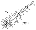
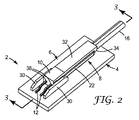
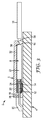
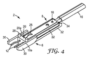
図1〜4は、本発明の態様による電気コネクタアセンブリの代表的な実施形態を示している。電気コネクタアセンブリ2は、プリント基板4と、プリント基板4に連結されたヘッダー6と、ヘッダー6と嵌合するように構成された電気ケーブル端子8と、を含む。ヘッダー6は、絶縁ハウジング10及び絶縁ハウジング10内に配置された複数のコンタクトピン12を含む。プリント基板4は、プリント基板グランドコンタクト14を含む。図3に最もよく示されるように、電気ケーブル端子8は、ヘッダー6及び電気ケーブル端子8が嵌合した構成にあるときに、コンタクトピン12及びプリント基板グランドコンタクト14と電気的に接触する。代替の実施形態において、電気ケーブル端子8は、少なくとも1つのコンタクトピン12及びプリント基板グランドコンタクト14と電気的に接触してもよい。
1-4 illustrate an exemplary embodiment of an electrical connector assembly according to aspects of the present invention. The
ヘッダー6及びプリント基板4と併せて用いることができる電気ケーブル端子は、米国特許第5,184,965号に記載されている同軸ケーブル用の遮蔽制御インピーダンス(SCI)コネクタと実質的に同様に構築することができる。特に、ヘッダー6及びプリント基板4と併せて用いることができる電気ケーブル端子の代表的な実施形態は、電気ケーブル端子8である。電気ケーブル端子8は、電気ケーブル端子8の前面8aが、絶縁ハウジング10の内壁20の前面20aに接するように、ヘッダー6に連結される。電気ケーブル端子8は、半田開口部18の使用を通じて、電気ケーブル16に連結される。電気ケーブル16は、単線ケーブル(例えば、単一同軸若しくは単一2軸)又は複数線ケーブル(例えば、複数同軸、複数2軸、又はツイストペア)であり得る。1つの実施形態では、電気ケーブル16は、1つ以上の伝導体及び1つ以上の伝導体を包囲するグランドシールド部を含む。図1〜4の実施形態では、電気ケーブル16は、2つの伝導体及び2つの伝導体を包囲するグランドシールド部を含む。
An electrical cable terminal that can be used in conjunction with the header 6 and the printed circuit board 4 is constructed substantially similar to a shielded controlled impedance (SCI) connector for coaxial cables described in US Pat. No. 5,184,965. can do. In particular, an exemplary embodiment of an electrical cable terminal that can be used in conjunction with the header 6 and the printed circuit board 4 is the
電気ケーブル端子8は、その中に取り付けられた内部コンタクト24を有する導電性ハウジング22を含む。内部コンタクト24はヘッダー6のコンタクトピン12と電気的接触をし、電気ケーブル端子8の長手方向軸に沿って存在するように構成される。各内部コンタクト24は、信号/電力コンタクトとして割り当てることができ、この場合には、内部コンタクト24は、電気ケーブル16の信号/電力コンダクタに電気的に接続されると共に、導電性ハウジング22から電気絶縁される。各内部コンタクト24は、グランドコンタクトとして割り当てることができ、この場合には、それは、電気ケーブル16のグランド導電体/シールド部に及び/又は導電性ハウジング22に電気的に接触する。
The
電気ケーブル端子8は、外部電気ケーブル端子グランドコンタクト26を更に含む。外部電気ケーブル端子グランドコンタクト26は、導電性ハウジング22の外側表面から延在し、図3に最も良く示されるように、ヘッダー6及び電気ケーブル端子8が嵌合した構成にあるとき、プリント基板4のグランドコンタクト14と電気的接触をするように構成される。図1〜4に示される電気コネクタアセンブリの代表的な実施形態において、プリント基板グランドコンタクト14は、単一のグランドパッドを含む。他の実施形態において、プリント基板グランドコンタクト14は、対象用途に好適であるように、1つ以上のグランドピン、導電性ストリップ又は複数のグランドパッドを含んでもよい。図示されている実施形態では、外部電気ケーブル端子グランドコンタクト26は、導電性ハウジング22から延在する弾性梁を含む。他の実施形態では、外部電気ケーブル端子グランドコンタクト26は、図示されたものとは異なる形体をとることができ、例えば、導電性ハウジング22から延在するヘルツバンプを含んでもよい。
The
更に図1〜4を参照して、ヘッダー6は、絶縁ハウジング10及び絶縁ハウジング10内に配置され、電気ケーブル端子8の内部コンタクト24と嵌合するために配列された複数のコンタクトピン12を含む。ヘッダー6のコンタクトピン12は、当該技術分野において既知のように、プリント基板4に接続される。コンタクトピン12は、プリント基板4の複数の電気配線(図示せず)のうちの1つ以上に電気的に接続するように構成される。ヘッダー6は、本明細書では、表面実装ピンヘッダーとして説明されているが、ヘッダー6は、貫通孔ピンヘッダー又は当該技術分野で既知のいずれか他の好適なタイプのヘッダーであってもよい。コンタクトピン12は、半田付け、プレス嵌め又はその他の任意の好適な方法によって、プリント基板4に接続され得る。図1〜4の実施形態では、ヘッダー6は、コンタクトピン12とプリント基板4との間の接続によって、並びに絶縁ハウジング10から延在する実装ポスト28によって、プリント基板4に固定される。実装ポスト28は、プリント基板4(図示せず)での孔内に挿入のために構成される。実装ポスト28は、プレス嵌め、接着剤又は他の好適な方法によって、プリント基板4内の孔に保持され得る。あるいは、ヘッダー6は、ヘッダー6をプリント基板4に固定するための追加の構造体を含んでもよく、又はコンタクトピン12とプリント基板4との間の接続のみによってプリント基板4に固定されてもよい。
1-4, the header 6 includes an insulating
ヘッダー6の絶縁ハウジング10は、2つの側壁30、側壁30間に配置された内壁20、内壁20から延在する弾性ラッチ32及び絶縁ハウジング10の底面10aから延在する実装ポスト28を含む。絶縁ハウジング10はモノリシックであり、しかし、別の方法として、スナップ嵌め、摩擦嵌め、機械的圧締め及び接着剤を含むがこれらに限定されない任意の好適な方法/構造体によって、複数の個々の要素(例えば、側壁30、内壁20、ラッチ32、及び実装ポスト28)として形成されてもよい。絶縁ハウジング10は、電気ケーブル端子8を受容しかつ位置決めするよう構成されており、これはラッチ32によって嵌合された構成に保持される。電気ケーブル端子8がヘッダー6内に挿入されるときに、電気ケーブル端子8の前側縁部8bは、ラッチ引き込み表面34と嵌合し、ラッチ32を電気ケーブル端子8の経路の外に偏向させる。電気ケーブル端子8が完全に挿入されると、ラッチ32は、元の(無偏向の)位置に戻り、ラッチフック部材36が、電気ケーブル端子8の後ろ側縁部8cと嵌合し、それによって、電気ケーブル端子がヘッダー6から抜けないようにする。電気ケーブル端子8は、電気ケーブル16を静かに引っ張りながら、単にラッチ32を(小型のツール又は爪で)偏向させて、電気ケーブル端子8の後ろ側縁部8cからラッチフック部材36を外すことによって、ヘッダー6から外すことができる。他の実施形態では、スナップ嵌め、摩擦嵌め、プレス嵌め、機械的圧締め及び接着剤が挙げられるが、これらに限らない任意の好適な方法/構造体によって、電気ケーブル端子8はヘッダー6の中に保持されることが可能である。絶縁ハウジング10の内壁20は、コンタクトピン12を位置決めし、保持するように構成された、複数のピン挿入開口部38を含む。コンタクトピン12は、プレス嵌め、摩擦嵌め、接着剤又はその他の好適な方法によって、挿入開口部38内に保持され得る。側壁30は、電気ケーブル端子8をヘッダー6内へ挿入するとき、電気ケーブル端子8の内部コンタクト24及びコンタクトピン12の整列を支援するように構成される。更に、側壁30は、ヘッダー6に安定性を提供するのを支援し、コンタクトピン12を損傷から保護する。
The insulating
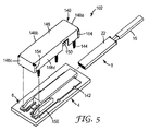
図5〜7は、本発明の態様による電気コネクタアセンブリの別の代表的な実施形態を図示する。電気コネクタアセンブリ102は、プリント基板4と、プリント基板4に連結されたヘッダー6と、ヘッダー6と嵌合するように構成された電気ケーブル端子8と、ヘッダー6及び電気ケーブル端子8を少なくとも部分的に包囲する導電性シールド部140と、を含む。プリント基板4、ヘッダー6及び電気ケーブル端子8はまた、図1〜4に図示され、上記において詳細に記載されている。この代表的な実施形態では、プリント基板4は更に、導電性シールド部140の第1の導電性シールド部グランドコンタクト144を受容するように構成された複数の孔142を含む。ヘッダー6及び電気ケーブル端子8が嵌合した構成にあるときに、電気ケーブル端子8は、コンタクトピン12及びプリント基板グランドコンタクト14と電気的に接触する。代替の実施形態において、電気ケーブル端子8は、少なくとも1つのコンタクトピン12及びプリント基板グランドコンタクト14と電気的に接触してもよい。
5-7 illustrate another exemplary embodiment of an electrical connector assembly according to aspects of the present invention. The
導電性シールド部140は、上壁146及び横方向に延在する側壁148a〜148d(本明細書においてまとめて「側壁148」と呼ばれる)を有する。図示された実施形態は、ヘッダー6の形状に実質的に対応する実質的に矩形の箱形の導電性シールド部140を画定する4つの側壁148を含むが、導電性シールド部140は、対象用途に好適な他の形状を画定する他の数の側壁を有してもよい。図示された実施形態において、上壁146、並びに側壁148b及び148dは、実質的に矩形の横断方向断面を画定するが、他の実施形態では、導電性シールド部140は、概ね曲線状の横断方向断面を有してもよい。側壁148の少なくとも1つは、電気ケーブル端子8の挿入及び抜取りを可能にするように構成される。図5〜7の実施形態では、側壁148aは、側壁148aが閉鎖位置(すなわち、上壁146に実質的に垂直に)と開放位置(すなわち、上壁146と実質的に平行)との間で旋回することができるように、上壁146から延在する。閉鎖位置では、側壁148aは、ヘッダー6及び電気ケーブル端子8を電磁干渉(EMI)放射から遮蔽するのに寄与する。開放位置では、側壁148aは、電気ケーブル端子8がヘッダー6内に挿入されること又はヘッダー6から抜き取られるのを可能にする。同様に、側壁148cは、側壁148cが閉鎖位置(すなわち、上壁146に実質的に垂直に)と開放位置(すなわち、上壁146と実質的に平行)との間で旋回できるように、上壁146から延在する。閉鎖位置では、側壁148cはヘッダー6及び電気ケーブル端子8を電磁干渉(EMI)放射から遮蔽するのに寄与する。開放位置では、側壁148cが、例えば修理又は交換のために、ヘッダー6のコンタクトピン12へのアクセスを可能にする。一部分において、電磁干渉(EMI)放射からの遮蔽を最適化するために、側壁148a及び148cは、側壁148b及び148dの一部分に重なり合うフランジ154を含む。側壁148aは、電気ケーブル16のための隙間を提供するように構成された開口部152を含む。1つの実施形態では、側壁148a内の開口部152は、側壁148aが旋回する必要なく、電気ケーブル端子8の挿入及び抜き出しを可能にするように成形されている。
The
導電性シールド部140は、側壁148b及び148dから延在する複数の第1の導電性シールド部グランドコンタクト144を含む。他の実施形態において、1つ以上の第1の導電性シールド部グランドコンタクト144は、1つ以上の側壁148から延在してもよい。第1の導電性シールド部グランドコンタクト144は、導電性シールド部140をプリント基板グランド要素(図示せず)に連結するように構成される。図示された実施形態では、第1の導電性シールド部グランドコンタクト144は、孔142を介して、半田付け、プレス嵌め又は他の好適な手法によって、導電性シールド部140をプリント基板グランド要素に連結するように構成された貫通孔コンタクトである。別の実施形態では、第1の導電性シールド部グランドコンタクトは、例えばプリント基板4上の表面実装パッドを介して、半田付け、機械的圧締め又は他の好適な手法によって、導電性シールド140をプリント基板グランド要素に連結するように構成された表面実装コンタクトであってもよい。
The
導電性シールド部140は、対向する側壁148b及び148d上に配置された、内側に突出する弾性的な第2の導電性シールド部グランドコンタクト150を更に含む。第2の導電性シールド部グランドコンタクト150は、ヘッダー6及び電気ケーブル端子8が嵌合した構成にあるときに、導電性シールド部140と電気ケーブル端子8との間に電気的接触を確立するように構成される。一部において電磁干渉(EMI)放射からの遮蔽を最適化するために、第2の導電性シールド部グランドコンタクト150は、側壁148b及び148dから剪断され、それによって側壁148b及び148dの実質的に全材料は存在したままである。他の実施形態において、導電性シールド部140は、単一の第2の導電性シールド部グランドコンタクト150のみを含んでもよい。図は、内側に突出する弾性的な第2の導電性シールド部グランドコンタクト150を含む導電性シールド部140を示すが、他のコンタクト要素構成、例えばヘルツバンプを弾性的な第2の導電性シールド部グランドコンタクト150の代わりに使用することは本発明の範囲内である。
The
一実施形態では、導電性シールド部140は、ヘッダー6及び電気ケーブル端子8が嵌合した構成にあるときに、電気ケーブル16のグランドシールド部と電気的に接触する。電気的接触は、直接行われてもよく、それによって、例えば、導電性シールド部140の側壁148aは、側壁148aの開口部152において電気ケーブル16のグランドシールド部と直接接触する。電気的接触は間接的に行われてもよく、それによって例えば導電性シールド部140の第2の導電性シールド部グランドコンタクト150が、電気ケーブル端子8の導電性ハウジング22と直接接触し、これは、電気ケーブル端子8の半田開口部18において、電気ケーブル16のグランドシールド部との直接接触である。
In one embodiment, the
一実施形態では、導電性シールド部140は、電磁干渉(EMI)吸収材料(図示せず)を含む。EMI吸収材料は、典型的に、電磁吸収性能を必要とする用途に使用される。それは、電気装置からの放射ノイズを、ブロードバンド高周波域のために抑制するように設計される。本発明の態様において使用することができるEMI吸収材料の例は、EMI Absorbers AB−2000シリーズ又はEMI Absorbers AB−5000シリーズであり、双方とも3M Company(St.Paul,MN)から市販されている。EMI Absorbers AB−2000シリーズは、アクリル系感圧性接着剤と共に、シリコーンゴム及び電磁材料から形成された薄型の可撓性裏材からなる。EMI Absorbers AB−5000シリーズは、アクリル接着剤系及び取り外し可能なライナーを備える、ポリマー樹脂中の可撓性の軟質金属フレーク充填剤からなる。一態様では、EMI吸収材料は、この吸収材料を、導電性シールド部140の内側表面の少なくとも一部分と実質的に対応する形状に切断した後、導電性シールド部140に接着することができる。
In one embodiment, the
一実施形態では、プリント基板4は、少なくとも部分的にヘッダー6及び電気ケーブル端子8を包囲する、例えば、図5に示される導電性シールド部要素156などの導電性シールド部要素を含む。導電性シールド部要素156は、任意の数の従来の付着又はエッチング技法、例えば気相堆積、化学エッチング等によってプリント基板4上に形成することができる。あるいは、導電性シールド部要素156は、金属、導電性ポリマー、セラミックス等とは別個の要素として形成されてもよい。導電性シールド部要素156は、半田、プレス嵌め、機械的圧締め、又は他の好適な手法によって、プリント基板4上に配置される、例えば、銅、銀、アルミニウム、又は他の伝導体の事前に形成された片を備えてもよい。導電性シールド部要素156は、図5に図示されるように、例えば、導電性シールド部140の側壁148によって画定される外辺部に実質的に対応する形状など、任意の好適な形状に形成され得る。導電性シールド部要素156は、ヘッダー6及び電気ケーブル端子8を電磁干渉(EMI)放射から遮蔽するのに寄与する。一実施形態では、導電性シールド部要素156は、プリント基板グランドコンタクト14の位置を占め、これによって、外部電気ケーブル端子グランドコンタクト26は、ヘッダー6及び電気ケーブル端子8が嵌合した構成にあるときに、導電性シールド部要素156と電気的に接触するように構成される。
In one embodiment, the printed circuit board 4 includes a conductive shield element such as, for example, the
一実施形態では、電気コネクタアセンブリ102は、導電性シールド部140の少なくとも一部分の周辺に配置され、導電性シールド部140をプリント基板グランド要素(図示せず)に連結するように構成された電磁干渉(EMI)ガスケット(図示せず)を含む。プリント基板グランド要素は、電気コネクタアセンブリ102の電気接地を促進し、並びに、例えば複数のグランドパッド及び/又はグランド配線となり得る。EMIガスケットは、複数の第1の導電性シールド部グランドコンタクト144の代わりに又はこれに加えて導電性シールド部140の周辺に配置されて、導電性シールド部140の周辺で実質的に連続の遮蔽を促進することができる。プリント基板4からの導電性シールド部140の容易な取り外しを促進するために、例えば、ヘッダー6及び/又は電気ケーブル端子8のアクセスを提供するために、複数の第1の導電性シールド部グランドコンタクト144の代わりに、EMIガスケットが導電性シールド部140の周辺に配置されてもよい。本発明の態様において使用できるEMIガスケットの例は、3M Company(St.Paul,MN)から市販されているXYZ−Axis Electrically Conductive Acrylic Pads(eCAP)である。eCAP製品は、EMI遮蔽に対して良好な導電性路を提供し、電子デバイスに接地する、自己固着性EMIガスケット又は接着剤転写テープである。eCAPは、接着剤マトリックスにわたって3次元構造において、固有の充填剤分布を達成する。高性能接着剤中のこの充填剤分布によって、テープは良好なxyz軸の伝導性及び良好な接着性能を有する。一実施形態では、eCAPは、導電性シールド部140の側壁148の縁部によって画定された形状と実質的に対応する形状に事前に切断される。この事前切断されたeCAPは次いで、導電性シールド部140をプリント基板4に接着するのに(及びプリント基板グランド要素に接触するのに)使用され、導電性シールド部140とプリント基板4との間に実質的に連続の遮蔽された接合部を形成する。本発明の態様において使用することができるEMIガスケットの別の例は、導電性分散粒子を含有するゴムエラストマーから作製されたガスケットである。一実施形態では、ゴムガスケットは、導電性シールド部140の周辺において適合する矩形の形状のスカートである。導電性シールド部140の側壁148の縁部を受容するゴムガスケット内に溝が形成される。ゴムガスケットは、導電性シールド部140とプリント基板4との間で圧縮可能であり、かつ圧縮され(及び印刷基板グランド要素に接触し)、導電性シールド部140とプリント基板4の間に実質的に連続の遮蔽された接合部を形成する。
In one embodiment, the
導電性シールド部要素156が存在する場合、EMIガスケットは導電性シールド部140と導電性シールド部要素156との間で、実質的に連続の遮蔽された接合部を形成してもよい。
If a
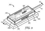
図8〜11は、本発明の態様による電気コネクタアセンブリの別の代表的な実施形態を図示する。電気コネクタアセンブリ202は、プリント基板204と、プリント基板204に連結されたヘッダー206と、ヘッダー206と嵌合するように構成された電気ケーブル端子8と、ヘッダー206及び電気ケーブル端子8を少なくとも部分的に包囲する導電性シールド部240と、を含む。プリント基板204は、導電性シールド部240の第1の導電性シールド部グランドコンタクト244を受容するように構成された複数の孔242を含む。電気ケーブル端子8はまた、図1〜4に図示され、上記詳細に記載されている。ヘッダー206は、絶縁ハウジング210及び絶縁ハウジング210内に配置された複数のコンタクトピン212を含む。ヘッダー206及び電気ケーブル端子8が嵌合した構成にあるときに、電気ケーブル端子8は、コンタクトピン212及び導電性シールド部240と電気的に接触する。
8-11 illustrate another exemplary embodiment of an electrical connector assembly according to aspects of the present invention. The
ヘッダー206は、絶縁ハウジング210及び絶縁ハウジング210内に配置され、電気ケーブル端子8の内部コンタクト24と嵌合するために配列された複数のコンタクトピン212を含む。ヘッダー206のコンタクトピン212は、当該技術分野において既知のように、プリント基板204に接続される。コンタクトピン212は、プリント基板204の複数の電気配線(図示せず)のうちの1つ以上に電気的に接続するように設計される。図8〜11の実施形態では、ヘッダー206は、コンタクトピン212とプリント基板204との間の接続によって、並びに絶縁ハウジング210から延在する実装ポスト228によってプリント基板204に固定される。実装ポスト228は、プリント基板204での孔258内に挿入されるように構成。実装ポスト228は、プレス嵌め、接着剤又はその他の好適な方法によって、プリント基板204の孔に保持され得る。
The
ヘッダー206の絶縁ハウジング210は、2つの側壁230、側壁230間に配置された内壁220、内壁220から延在する弾性ラッチ232及び絶縁ハウジング210の底面210aから延在する実装ポスト228を含む。縁性ハウジング210はモノリシックである。絶縁ハウジング210は、電気ケーブル端子8を受容しかつ位置決めするよう構成されており、これはラッチ232によって嵌合した構成に保持される。電気ケーブル端子8がヘッダー206内に挿入されるときに、電気ケーブル端子8の前側縁部8bは、ラッチ引き込み表面234と嵌合し、ラッチ232を電気ケーブル端子8の経路の外に偏向させる。電気ケーブル端子8が完全に挿入されると、ラッチ232は、元の(無偏向の)位置に戻り、ラッチフック部材236が、電気ケーブル端子8の後ろ側縁部8cと嵌合し、それによって、電気ケーブル端子がヘッダー206から抜けないようにする。電気ケーブル端子8は、電気ケーブル16を静かに引っ張りながら、単にラッチ232を(小型のツール又は爪で)偏向させて、電気ケーブル端子8の後側縁部8cからラッチフック部材236を引き離すことによって、ヘッダー206から外すことができる。ラッチ232は、ヘッダー206及び電気ケーブル端子8が嵌合した構成にあるときに、第2の導電性シールド部グランドコンタクト250(以下に記載)が、導電性シールド部240と電気ケーブル端子8との間に電気的接続を確立するのを可能にするように構成されたラッチ開口部256を更に含む。絶縁ハウジング210の内壁220は、コンタクトピン212を位置決めし、保持するように構成された、複数のピン挿入開口部238を含む。コンタクトピン212は、プレス嵌め、摩擦嵌め、接着剤又はその他の好適な方法によって、挿入開口部238に保持され得る。側壁230は、電気ケーブル端子8をヘッダー206へ挿入するとき、電気ケーブル端子8の内部コンタクト224及びコンタクトピン212の整列を支援するように構成される。更に、側壁230は、ヘッダー206に安定性を提供するのを支援し、コンタクトピン212を損傷から保護する。
The insulating
更に図8〜11を参照すると、導電性シールド部240は2部のシールド部であり、上方シールド部分240a及び下方シールド部分240bを含む。上方シールド部分240aは上壁246及び横方向に延在する上方シールド部側壁248a〜248dを有する。下方シールド部分240bは底壁247及び横方向に延在する下方シールド部側壁248e〜248gを有する。上方シールド部側壁248a〜248d及び下方シールド部側壁248e〜248gは、本明細書においてまとめて「側壁248」と呼ばれる。図示された実施形態は、ヘッダー206の形状に実質的に対応する実質的に矩形の箱形の導電性シールド部240を画定する7つの側壁248を含むが、導電性シールド部240は、対象用途に好適な他の形状を画定する他の数の側壁を有してもよい。図示された実施形態において、上壁246、底壁247、並びに側壁248b/248e及び248d/248gは、実質的に矩形の横断方向断面を画定し、他の実施形態では、導電性シールド部240は、概ね曲線状の横断方向断面を有してもよい。図8〜11の実施形態では、上方シールド部分240a及び下方シールド部分240bが組み立てられた構成にあるとき、上方シールド部側壁248b〜248dは、それらが下方シールド部側壁248e〜248gと重なり合うように、上壁246から延在する。上方シールド部分240a及び下方シールド部分240bが組み立てられた構成にあるとき、上方シールド部分240aは、ヘッダー206及び電気ケーブル端子8の電磁干渉(EMI)放射からの遮蔽に寄与する。上方シールド部分240a及び下方シールド部分240bが組み立てられていない構成にあるとき、電気ケーブル端子8は、ヘッダー206内に挿入されることができ、又はこれから取り出すことができ、ヘッダー206のコンタクトピン212は、例えば修理又は交換のためにアクセスすることができる。一部分において、電磁干渉(EMI)放射からの遮蔽を最適化するために、上方シールド部側壁248a及び248cは、上方シールド部側壁248b及び248dの一部分に重なり合うフランジ254を含む。上方シールド部側壁248aは、電気ケーブル16のための隙間を提供するように構成された開口部252を含む。一実施形態では、上方シールド部分240a及び下方シールド部分240bは、上方シールド部分240a及び下方シールド部分240bを、組み立てられた構成に保持するように構成された協働固定要素260を含む。図8〜11の実施形態では、上方シールド部分240aは、対向する下方シールド部側壁248e及び248g上の対応する固定ストリップ260bと嵌合する固定開口部260aを、対向する上方シールド部側壁248b及び248d上に含む。他の実施形態では、スナップ嵌め、摩擦嵌め、プレス嵌め、機械的クランプ、及び接着剤が挙げられるが、これらに限らない任意の好適な方法/構造体によって、上方シールド部分240a及び下方シールド部分240bは、組み立てられた構成に保持されることが可能である。
8 to 11, the
導電性シールド部240は、下方シールド部側壁248e及び248gから延在する、複数の第1の導電性シールド部グランドコンタクト244を含む。他の実施形態において、1つ以上の第1の導電性シールド部グランドコンタクト244は、1つ以上の側壁248から延在してもよい。第1の導電性シールド部グランドコンタクト244は、導電性シールド部240をプリント基板グランド要素(図示せず)に連結するように構成される。図示された実施形態では、第1の導電性シールド部グランドコンタクト244は、孔242を介して、半田付け、プレス嵌め、又は他の好適な手法によって、導電性シールド部240をプリント基板グランド要素に連結するように構成された貫通孔コンタクトである。
The
導電性シールド部240は、上壁246上に配置された、内側に突出する弾性的な第2の導電性シールド部グランドコンタクト250を更に含む。第2の導電性シールド部グランドコンタクト250は、ヘッダー206及び電気ケーブル端子8が嵌合した構成にあるときに、導電性シールド部240と電気ケーブル端子8との間に電気的接触を確立するように構成される。一部において、電磁干渉(EMI)放射からの遮蔽を最適化するために、第2の導電性シールド部グランドコンタクト250は、上壁246から剪断され、それによって上壁246の実質的に全材料は存在したままである。他の実施形態において、導電性シールド部240は、1を超える第2の導電性シールド部グランドコンタクト250を含んでもよい。
The
図8〜11に図示された実施形態では、底壁247は、任意のブリッジ部分247aを含む。ブリッジ部分247aは、図11に最も良く示されるように、ヘッダー206及び電気ケーブル端子8が嵌合した構成にあるときに、電気ケーブル端子8の外部電気ケーブル端子グランドコンタクト26と電気的接触をするように構成される。ブリッジ部分247aがないとき、外部電気ケーブル端子グランドコンタクト26は、例えば、プリント基板4のグランドコンタクト14などのグランドコンタクトと電気的接触をするように構成されてもよい。
In the embodiment illustrated in FIGS. 8-11, the
本明細書で説明した実施形態及び実現形態の各々において、電気コネクタアセンブリ及びその素子の種々の構成要素は、任意の好適な材料で形成されている。材料は意図される用途によって選択され、金属及び非金属の両方を含んでもよい(例えば、ポリマー、ガラス、及びセラミックスが挙げられるがこれらに限定されない非導電性材料の、いずれか1つの組み合わせ)。一実施形態では、導電性構成要素、例えば導電性ハウジング10などは、射出成形、押出成形、鋳造、機械加工などの方法によって、ポリマー材料から形成され、その一方で導電性構成要素、例えば、導電性ハウジング22、内部コンタクト24、導電性シールド部140、及びコンタクトピン12などは、成形、鋳造、鍛造、機械加工等によって形成される。材料選定は、少し挙げただけでも、化学薬品暴露条件、温度及び湿度条件を含む環境暴露条件、難燃性要件、材料強度、並びに剛性などを含むがこれらに限定されない要因に依存する。
In each of the embodiments and implementations described herein, the various components of the electrical connector assembly and its elements are formed of any suitable material. The material is selected depending on the intended use and may include both metals and non-metals (eg, any one combination of non-conductive materials including, but not limited to, polymers, glasses, and ceramics). In one embodiment, the conductive component, such as the
好ましい実施形態の説明の目的のために、特定の実施形態を本明細書において例示し記述したが、同じ目的を達成すると予測される種々多様な代替及び/又は同等の実施が、本発明の範囲を逸脱することなく、図示及び説明された特定の実施形態に置き換わり得ることを、当業者は理解するであろう。機械、電気機械、及び電気分野における当業者であれば、本発明が非常に広範囲に及ぶ多様な実施形態において実施されてもよいことを、容易に理解するであろう。本出願は、本明細書で説明された好ましい実施形態のいかなる翻案又は変形をも包含すべく意図されている。したがって、本発明が請求項及びその等価物によってのみ限定されることを、明示的に意図するものである。 While specific embodiments have been illustrated and described herein for the purpose of illustrating the preferred embodiments, various alternative and / or equivalent implementations that are expected to achieve the same objectives are within the scope of the present invention. Those skilled in the art will appreciate that the specific embodiments shown and described may be substituted without departing from the invention. Those skilled in the mechanical, electromechanical, and electrical arts will readily appreciate that the present invention may be implemented in a very wide variety of embodiments. This application is intended to cover any adaptations or variations of the preferred embodiments described herein. Therefore, it is manifestly intended that this invention be limited only by the claims and the equivalents thereof.
Claims (20)
前記プリント基板に連結され、かつ絶縁ハウジング及び前記絶縁ハウジング内に配置された複数のコンタクトピンを含むヘッダーと、
前記ヘッダーと嵌合するように構成された電気ケーブル端子と、を含む、電気コネクタアセンブリであって、
前記ヘッダー及び電気ケーブル端子が、前記ヘッダー及び電気ケーブル端子が嵌合した構成にあるときに、前記電気ケーブル端子が、少なくとも1つの前記コンタクトピン及び前記プリント基板グランドコンタクトと電気的に接触するように構成されている、電気コネクタアセンブリ。 A printed circuit board having a printed circuit board ground contact;
A header coupled to the printed circuit board and including an insulating housing and a plurality of contact pins disposed in the insulating housing;
An electrical cable assembly configured to mate with the header, the electrical connector assembly comprising:
When the header and the electrical cable terminal are in a configuration in which the header and the electrical cable terminal are fitted, the electrical cable terminal is in electrical contact with at least one of the contact pin and the printed circuit board ground contact. An electrical connector assembly configured.
前記プリント基板に連結され、かつ絶縁ハウジング及び前記絶縁ハウジング内に配置された複数のコンタクトピンを備える、ヘッダーと、
前記ヘッダーと嵌合するように構成された電気ケーブル端子と、
前記ヘッダー及び電気ケーブル端子を少なくとも部分的に包囲する導電性シールド部と、を含む、電気コネクタアセンブリであって、
前記ヘッダー及び電気ケーブル端子が、前記ヘッダー及び電気ケーブル端子が嵌合した構成にあるときに、前記電気ケーブル端子が、少なくとも1つの前記コンタクトピン及び前記プリント基板グランドコンタクトと電気的に接触するように構成されている、電気コネクタアセンブリ。 A printed circuit board having a printed circuit board ground contact;
A header coupled to the printed circuit board and comprising an insulating housing and a plurality of contact pins disposed within the insulating housing;
An electrical cable terminal configured to mate with the header;
An electrical connector assembly comprising: a conductive shield at least partially surrounding the header and the electrical cable terminal;
When the header and the electrical cable terminal are in a configuration in which the header and the electrical cable terminal are fitted, the electrical cable terminal is in electrical contact with at least one of the contact pin and the printed circuit board ground contact. An electrical connector assembly configured.
前記プリント基板に連結され、かつ絶縁ハウジング及び前記絶縁ハウジング内に配置された複数のコンタクトピンを備える、ヘッダーと、
前記ヘッダーと嵌合するように構成され、かつ電気ケーブル端子、及び1つ以上の伝導体及び前記1つ以上の伝導体を包囲するグランドシールド部を含む電気ケーブル、を備える、電気ケーブルアセンブリと、
前記プリント基板グランド要素に連結され、かつ前記ヘッダー及び電気ケーブルアセンブリを少なくとも部分的に包囲する、導電性シールド部と、を含む、電気コネクタアセンブリであって、
前記ヘッダー、電気ケーブルアセンブリ及び導電性シールド部は、前記電気ケーブル端子が、少なくとも1つの前記コンタクトピン及び前記プリント基板グランドコンタクトと電気的接触をするように構成され、かつ前記導電性シールド部は、前記ヘッダー及び電気ケーブルアセンブリが嵌合した構成にあるときに、前記電気ケーブル端子及び前記グランドシールド部のうちの少なくとも1つと電気的接触をする、電気コネクタアセンブリ。 A printed circuit board having a printed circuit board ground contact and a printed circuit board ground element;
A header coupled to the printed circuit board and comprising an insulating housing and a plurality of contact pins disposed within the insulating housing;
An electrical cable assembly configured to mate with the header and comprising an electrical cable terminal and one or more conductors and a ground shield portion surrounding the one or more conductors;
An electrical connector assembly coupled to the printed circuit board ground element and at least partially surrounding the header and electrical cable assembly;
The header, the electrical cable assembly, and the conductive shield are configured such that the electrical cable terminal is in electrical contact with at least one of the contact pins and the printed circuit board ground contact, and the conductive shield is An electrical connector assembly that makes electrical contact with at least one of the electrical cable terminal and the ground shield portion when the header and electrical cable assembly are in a mated configuration.
Applications Claiming Priority (3)
| Application Number | Priority Date | Filing Date | Title |
|---|---|---|---|
| US12/192,265 | 2008-08-15 | ||
| US12/192,265 US7892007B2 (en) | 2008-08-15 | 2008-08-15 | Electrical connector assembly |
| PCT/US2009/050375 WO2010019332A2 (en) | 2008-08-15 | 2009-07-13 | Electrical connector assembly |
Publications (1)
| Publication Number | Publication Date |
|---|---|
| JP2012500451A true JP2012500451A (en) | 2012-01-05 |
Family
ID=41669548
Family Applications (1)
| Application Number | Title | Priority Date | Filing Date |
|---|---|---|---|
| JP2011523021A Pending JP2012500451A (en) | 2008-08-15 | 2009-07-13 | Electrical connector assembly |
Country Status (7)
| Country | Link |
|---|---|
| US (1) | US7892007B2 (en) |
| EP (1) | EP2321875A4 (en) |
| JP (1) | JP2012500451A (en) |
| CN (1) | CN102177619A (en) |
| CA (1) | CA2733596A1 (en) |
| TW (1) | TW201014079A (en) |
| WO (1) | WO2010019332A2 (en) |
Cited By (1)
| Publication number | Priority date | Publication date | Assignee | Title |
|---|---|---|---|---|
| JP2016048681A (en) * | 2014-08-27 | 2016-04-07 | ティーイー コネクティビティ ジャーマニー ゲゼルシャフト ミット ベシュレンクテル ハフツンクTE Connectivity Germany GmbH | Vehicular cable assembly |
Families Citing this family (27)
| Publication number | Priority date | Publication date | Assignee | Title |
|---|---|---|---|---|
| DE102009018715A1 (en) * | 2009-04-27 | 2010-11-04 | Phoenix Contact Gmbh & Co. Kg | Fastening device for fastening a connector plug to a base housing |
| KR101606371B1 (en) * | 2009-10-13 | 2016-03-28 | 삼성전자주식회사 | Ground Construction of Connector For Portable Device |
| US7976340B1 (en) * | 2010-03-12 | 2011-07-12 | Tyco Electronics Corporation | Connector system with electromagnetic interference shielding |
| TWM395946U (en) * | 2010-05-24 | 2011-01-01 | Ks Terminals Inc | Latched connector assembly |
| US8513955B2 (en) | 2010-09-28 | 2013-08-20 | Tyco Electronics Corporation | SSL budgeting and coding system for lighting assembly |
| US8277252B2 (en) * | 2010-10-01 | 2012-10-02 | Tyco Electronics Corporation | Electrical connector assembly |
| US9713295B2 (en) | 2012-06-21 | 2017-07-18 | Apple Inc. | Tape-based grounding structures |
| JP5890157B2 (en) * | 2011-11-25 | 2016-03-22 | 日本航空電子工業株式会社 | Wire-to-board connector |
| CN103376841A (en) * | 2012-04-12 | 2013-10-30 | 鸿富锦精密工业(深圳)有限公司 | Electronic device shell with cable sorting rack |
| US8840432B2 (en) * | 2012-04-24 | 2014-09-23 | Tyco Electronics Corporation | Circuit board and wire assembly |
| TWM442618U (en) * | 2012-05-14 | 2012-12-01 | Hon Hai Prec Ind Co Ltd | Electrical connector |
| US8932078B1 (en) * | 2012-09-14 | 2015-01-13 | Juniper Networks, Inc. | Apparatus, methods, and systems for retaining a cable |
| JP5904106B2 (en) * | 2012-11-30 | 2016-04-13 | 日立金属株式会社 | Cable connector, cable assembly, and method of manufacturing cable assembly |
| TWI593199B (en) * | 2013-01-08 | 2017-07-21 | 鴻騰精密科技股份有限公司 | Electrical connector |
| US9313934B2 (en) * | 2013-03-15 | 2016-04-12 | Autoliv Asp, Inc. | Dispensible electrical gasket, electronic module having dispensible electrical gasket, and method of fabricating same |
| WO2016072986A1 (en) * | 2014-11-06 | 2016-05-12 | Ardent Concepts, Inc. | Controlled-impedance cable termination using compliant interconnect elements |
| DE102014224475A1 (en) | 2014-12-01 | 2016-06-02 | Zf Friedrichshafen Ag | Circuit carrier and method for producing and for electrically connecting a circuit carrier |
| EP3076492B1 (en) * | 2015-03-30 | 2020-10-28 | Aptiv Technologies Limited | Electrical connector system with laterally protruding releasing arm |
| US9755334B2 (en) | 2015-06-25 | 2017-09-05 | Intel Corporation | Retention mechanism for shielded flex cable to improve EMI/RFI for high speed signaling |
| GB2547958B (en) * | 2016-03-04 | 2019-12-18 | Commscope Technologies Llc | Two-wire plug and receptacle |
| CN206282999U (en) * | 2016-11-11 | 2017-06-27 | 番禺得意精密电子工业有限公司 | Connector assembly |
| CN110546822A (en) | 2017-04-24 | 2019-12-06 | 康普技术有限责任公司 | Connector for single twisted conductor pairs |
| US10573996B2 (en) * | 2017-11-28 | 2020-02-25 | International Business Machines Corporation | Integrated force gauge cable mechanism |
| CN109088197B (en) * | 2018-07-27 | 2022-06-21 | 富士康(昆山)电脑接插件有限公司 | Electric connector assembly and electric connector system |
| AU2020239985A1 (en) | 2019-03-15 | 2021-08-26 | Commscope Technologies Llc | Connectors and contacts for a single twisted pair of conductors |
| US11646514B2 (en) * | 2020-08-10 | 2023-05-09 | Lear Corporation | Surface mount technology terminal header and method for providing an electrical connection to a printed circuit board |
| CN113224598B (en) * | 2021-04-30 | 2023-10-20 | 珠海领翌科技有限公司 | Cable connector and electronic device |
Family Cites Families (21)
| Publication number | Priority date | Publication date | Assignee | Title |
|---|---|---|---|---|
| US5766027A (en) | 1995-12-21 | 1998-06-16 | The Whitaker Corporation | Cable assembly with equalizer board |
| JP3349059B2 (en) * | 1997-03-24 | 2002-11-20 | 株式会社アイペックス | Connector with shield cover. |
| US6524134B2 (en) | 1999-12-01 | 2003-02-25 | Tyco Electronics Corporation | Pluggable module and receptacle |
| US6517382B2 (en) | 1999-12-01 | 2003-02-11 | Tyco Electronics Corporation | Pluggable module and receptacle |
| US6368120B1 (en) | 2000-05-05 | 2002-04-09 | 3M Innovative Properties Company | High speed connector and circuit board interconnect |
| US6682368B2 (en) | 2000-05-31 | 2004-01-27 | Tyco Electronics Corporation | Electrical connector assembly utilizing multiple ground planes |
| US6431887B1 (en) | 2000-05-31 | 2002-08-13 | Tyco Electronics Corporation | Electrical connector assembly with an EMI shielded plug and grounding latch member |
| US6508678B1 (en) * | 2000-08-31 | 2003-01-21 | Advanced Connecteck Inc. | Electrical connector assembly |
| AU2003220046A1 (en) * | 2002-03-06 | 2003-09-22 | Tyco Electronics Corporation | Transceiver module assembly ejector mechanism |
| US6666720B1 (en) | 2002-07-31 | 2003-12-23 | Tyco Electronics Corporation | Electrical connector receptacle with module kickout mechanism |
| US6655995B1 (en) | 2002-07-31 | 2003-12-02 | Tyco Electronics Corporation | Electrical connector receptacle cage with interlocking upper and lower shells |
| US6805573B2 (en) | 2002-12-04 | 2004-10-19 | Tyco Electronics Corporation | Connector module with lever actuated release mechanism |
| US6943287B2 (en) * | 2003-03-31 | 2005-09-13 | Molex Incorporated | Shielding cage with improved EMI shielding gasket construction |
| US7004793B2 (en) * | 2004-04-28 | 2006-02-28 | 3M Innovative Properties Company | Low inductance shielded connector |
| NL1027044C2 (en) * | 2004-09-15 | 2006-03-16 | Framatome Connectors Int | Connector and connector assembly comprising conduits with at least one opening. |
| US7226314B2 (en) * | 2005-02-23 | 2007-06-05 | Molex Incorporated | Connector and guide placement member |
| US7281938B1 (en) * | 2005-08-11 | 2007-10-16 | Hon Hai Precision Ind. Co., Ltd. | Small size electrical connector assembly |
| US20070141871A1 (en) * | 2005-12-19 | 2007-06-21 | 3M Innovative Properties Company | Boardmount header to cable connector assembly |
| JP4703454B2 (en) * | 2006-03-27 | 2011-06-15 | 富士通株式会社 | Cage mounting structure for optical modules |
| TWI313527B (en) * | 2006-11-03 | 2009-08-11 | Ks Terminals Inc | Electrical connector and method of fabricating the same |
| US7445471B1 (en) * | 2007-07-13 | 2008-11-04 | 3M Innovative Properties Company | Electrical connector assembly with carrier |
-
2008
- 2008-08-15 US US12/192,265 patent/US7892007B2/en not_active Expired - Fee Related
-
2009
- 2009-07-13 CA CA2733596A patent/CA2733596A1/en not_active Abandoned
- 2009-07-13 WO PCT/US2009/050375 patent/WO2010019332A2/en active Application Filing
- 2009-07-13 CN CN2009801402254A patent/CN102177619A/en active Pending
- 2009-07-13 JP JP2011523021A patent/JP2012500451A/en active Pending
- 2009-07-13 EP EP09807024A patent/EP2321875A4/en not_active Withdrawn
- 2009-07-27 TW TW098125251A patent/TW201014079A/en unknown
Cited By (1)
| Publication number | Priority date | Publication date | Assignee | Title |
|---|---|---|---|---|
| JP2016048681A (en) * | 2014-08-27 | 2016-04-07 | ティーイー コネクティビティ ジャーマニー ゲゼルシャフト ミット ベシュレンクテル ハフツンクTE Connectivity Germany GmbH | Vehicular cable assembly |
Also Published As
| Publication number | Publication date |
|---|---|
| EP2321875A2 (en) | 2011-05-18 |
| TW201014079A (en) | 2010-04-01 |
| CN102177619A (en) | 2011-09-07 |
| WO2010019332A2 (en) | 2010-02-18 |
| US7892007B2 (en) | 2011-02-22 |
| WO2010019332A3 (en) | 2010-04-15 |
| US20100041273A1 (en) | 2010-02-18 |
| EP2321875A4 (en) | 2012-01-25 |
| CA2733596A1 (en) | 2010-02-18 |
Similar Documents
| Publication | Publication Date | Title |
|---|---|---|
| JP2012500451A (en) | Electrical connector assembly | |
| US7211739B1 (en) | Electromagnetic interference (EMI) shield for a cable-bulkhead interface | |
| KR101121836B1 (en) | Connector apparatus | |
| TWI543484B (en) | An innovative cable termination scheme | |
| TWI424638B (en) | Performance enhancing contact module assemblies | |
| TWI253212B (en) | Connector having a simple structure assuring a stable mounting operation | |
| JP2004200454A (en) | Noise suppression structure for shielded cable | |
| JPH04229573A (en) | Connector with earthing structure | |
| CN106025719A (en) | Electrical connector and interconnection system having resonance control | |
| US5151036A (en) | Connectors with ground structure | |
| US5823826A (en) | Filtered circuit connector with frame | |
| US5261829A (en) | Connectors with ground structure | |
| JPS58123683A (en) | Plug connecting device | |
| US6707675B1 (en) | EMI containment device and method | |
| KR100585938B1 (en) | Connector having a shell which can readily be fixed to a connector housing | |
| US6210228B1 (en) | Shielded electrical connector | |
| EP4280393A1 (en) | Connector assembly including receptacle connector and plug connector, and plug connector | |
| JP3370280B2 (en) | Narrow-pitch multistage board connector and shield shell fittings used therefor | |
| JP2003508936A (en) | Assembly of electrical component having EMI suppression wiring plate, method of manufacturing the same, and EMI suppression wiring plate | |
| JP2001230022A (en) | Cable connector for shielded cable | |
| US6200165B1 (en) | Shielded electrical connector with a folded wall | |
| US20230132094A1 (en) | High speed electrical connector | |
| US20240322497A1 (en) | Connector Assembly Including Receptacle Connector and Plug Connector, and Plug Connector | |
| JPH0676887A (en) | Connector device | |
| JP2001185303A (en) | Electronics and connector for it |