JP2012252361A - Display device - Google Patents
Display device Download PDFInfo
- Publication number
- JP2012252361A JP2012252361A JP2012188685A JP2012188685A JP2012252361A JP 2012252361 A JP2012252361 A JP 2012252361A JP 2012188685 A JP2012188685 A JP 2012188685A JP 2012188685 A JP2012188685 A JP 2012188685A JP 2012252361 A JP2012252361 A JP 2012252361A
- Authority
- JP
- Japan
- Prior art keywords
- film
- electrode
- liquid crystal
- drain electrode
- thickness
- Prior art date
- Legal status (The legal status is an assumption and is not a legal conclusion. Google has not performed a legal analysis and makes no representation as to the accuracy of the status listed.)
- Withdrawn
Links
Images


Abstract
Description
本明細書で開示する発明は、アクティブマトリクス型の反射型液晶パネルの構造に関す
る。
The invention disclosed in this specification relates to a structure of an active matrix reflective liquid crystal panel.
図8に従来より公知のアクティブマトリクス型の反射型液晶パネルの概略の断面を示す
。図8に示す構成では、ソース領域部708、ゲイト電極部709、ドレイン領域部71
0の領域でなるTFT(薄膜トランジスタ)が配置され、さらにこのTFTのソース領域
部710に反射画素電極706が接続された構造となっている。
FIG. 8 shows a schematic cross section of a conventionally known active matrix reflective liquid crystal panel. In the configuration shown in FIG. 8, a
A TFT (thin film transistor) having a 0 region is disposed, and a
一般にこのような構造においては、ソース電極部708、ゲイト電極部709、ドレイ
ン電極部710との上面の平坦性や、画素領域711と他の領域との間における平坦性は
、図示されるようにあまり考慮されていない。
In general, in such a structure, the flatness of the top surfaces of the
この平坦性の乱れ(即ち凹凸)は、300nm〜700nm程度となるのが普通である
。
The flatness irregularity (that is, unevenness) is usually about 300 nm to 700 nm.
このような凹凸の存在は、液晶分子の乱れ707の原因となる。しかし、液晶層の厚さ
が7μmや8μm以上というように厚い場合は、上記の凹凸の影響は表示にそれ程大きな
影響を与えない。
The presence of such irregularities causes the
即ち、液晶分子の乱れの影響は液晶層の厚さ方向全体には及ばず、そのことが表示に与
える影響も少ない。
That is, the influence of the disturbance of the liquid crystal molecules does not reach the entire thickness direction of the liquid crystal layer, and the influence on the display is small.
しかし、近年は高画質の追求、及びそれに伴う液晶材料の進歩により、より液晶層の厚
さを狭くすることが要求されている。
However, in recent years, it has been required to further reduce the thickness of the liquid crystal layer due to the pursuit of high image quality and the accompanying progress in liquid crystal materials.
特に反射型の液晶パネルにおいては、光が液晶層を2回通過するので、透過型のものに
比較してその厚さを1/2とすることが要求される。(実際にはそう単純な話にはならな
いが、概略そうであるといえる)
In particular, in a reflective liquid crystal panel, light passes through the liquid crystal layer twice, so that the thickness is required to be halved compared to a transmissive type. (It's not really a simple story, but it seems to be roughly)
これまで、反射型の液晶パネルは、微細な表示特性や高速動画表示は求められていなか
った。従って、無理して液晶層の厚さを薄くして、表示特性を向上させる必要はなかった
。
Up to now, reflective liquid crystal panels have not been required to have fine display characteristics and high-speed moving image display. Therefore, it was not necessary to forcibly reduce the thickness of the liquid crystal layer and improve the display characteristics.
本発明者らの知見によれば、反射型の液晶パネルは、投影型のプロジェクターに利用す
ることが適していることが判明している。
According to the knowledge of the present inventors, it has been found that the reflective liquid crystal panel is suitable for use in a projection type projector.
これは、プロジェクターには、画面サイズが小型のものが要求(画面サイズが大きいと
光学系が高価になる)され、また反射型の液晶パネルは、画面サイズが2.5 インチ対角以
下というような小型のものに関しては、透過型よりも画素の開口率を高くできるからであ
る。
This is because projectors are required to have a small screen size (the optical system becomes expensive when the screen size is large), and the reflective LCD panel is small, such as a screen size of 2.5 inches diagonal or less. This is because the aperture ratio of the pixel can be higher than that of the transmissive type.
一般に画面サイズが小さくなると、透過型では、TFT、配線、容量電極といった光が
透過しない領域の面積の割合が大きくなり、また透過部分の透過損失も顕在化する。(本
出願人らの算出によれば、画面サイズが2.5 インチ以下になるとこの傾向が顕在化する)
In general, when the screen size is reduced, in the transmissive type, the ratio of the area where light is not transmitted, such as TFT, wiring, and capacitive electrode, increases, and the transmission loss of the transmissive portion becomes obvious. (According to the calculations by the applicants, this tendency becomes apparent when the screen size is 2.5 inches or less.)
他方、反射型では、反射電極の下部にTFTや配線や容量電極を配置させることができ
、また反射電極の反射損失も透過型の透過損失に比べればはるかに小さくできる。
On the other hand, in the reflective type, TFTs, wirings, and capacitive electrodes can be arranged below the reflective electrode, and the reflective loss of the reflective electrode can be made much smaller than that of the transmissive transmission loss.
プロジェクタには、高微細な表示を行う性能が要求される。従って、プロジェクターに
利用する反射型の液晶パネルには、高い表示特性が要求される。特にプロジェクターの場
合は、画像が数十倍〜100倍以上に拡大されるので、この要求はシビアなものとなる。
A projector is required to have a performance for performing high-definition display. Therefore, high display characteristics are required for the reflective liquid crystal panel used in the projector. In particular, in the case of a projector, the image is magnified several tens to 100 times or more, so this requirement becomes severe.
このような理由により、反射型の液晶パネルにも高い表示特性が要求され、それを実現
するために液晶層の厚さを薄くことが要求される。
For this reason, the reflective liquid crystal panel is also required to have high display characteristics, and in order to realize this, the liquid crystal layer is required to be thin.
本出願人らの知見によれば、要求される表示特性を得るには、反射型の液晶パネルの場
合、液晶層の厚さは2〜4μm程度とすることが求められる。これは、コントラストを最
大とする条件から要求されることである。
According to the knowledge of the present applicants, in order to obtain the required display characteristics, in the case of a reflective liquid crystal panel, the thickness of the liquid crystal layer is required to be about 2 to 4 μm. This is required from the condition that maximizes the contrast.
このような場合、液晶層に接する面における凹凸の段差が液晶層の10%以上あると、
液晶の配向の乱れが顕著になり、画質の低下(特にコントラストの低下)が著しくなる。
In such a case, when the uneven step on the surface in contact with the liquid crystal layer is 10% or more of the liquid crystal layer,
The disorder of the alignment of the liquid crystal becomes remarkable, and the image quality (particularly, the contrast) is remarkably deteriorated.
液晶層の厚さdはコントラストを最大とする条件によって定められる。コントラストを
最大にする条件は、液晶材料によって決まるΔn(リタデーション)と液晶層の厚さdと
の積(Δnd)によって決まる。しかしこの値は、波長依存性があり、その依存性が液晶
材料によって異なるという厄介な性質があり、最適化することは簡単ではない。
The thickness d of the liquid crystal layer is determined by the condition that maximizes the contrast. The condition for maximizing the contrast is determined by the product (Δnd) of Δn (retardation) determined by the liquid crystal material and the thickness d of the liquid crystal layer. However, this value has a wavelength dependency and has a troublesome property that the dependency varies depending on the liquid crystal material, and it is not easy to optimize.
図7に示すのは、反射型の液晶パネルを想定したシュミレーション結果である。ここで
、横軸は入射光の波長であり、縦軸は入射光と出力光との比(透過率と定義する)である
。
FIG. 7 shows a simulation result assuming a reflective liquid crystal panel. Here, the horizontal axis represents the wavelength of incident light, and the vertical axis represents the ratio between incident light and output light (defined as transmittance).
図7中のプロット点は、液晶層の厚さを変化させた場合のものである。 Plot points in FIG. 7 are obtained when the thickness of the liquid crystal layer is changed.
人間の目の波長感度は、450nm〜680nm程度の範囲にあり、550nm付近に
その最大値を有する。
The wavelength sensitivity of the human eye is in the range of about 450 nm to 680 nm, and has a maximum value near 550 nm.
従って、カラー表示をさせようとする場合、図7に示すような曲線は、450nm〜6
80nmの範囲における透過率が極力平坦であることが重要となる。特に波長感度の高い
500nm〜600nmの範囲における平坦性が重要となる。
Therefore, when color display is to be performed, the curve as shown in FIG.
It is important that the transmittance in the 80 nm range is as flat as possible. In particular, flatness in the range of 500 nm to 600 nm with high wavelength sensitivity is important.
また、当然のことながら透過率が極力高いこと(即ち透過損失が極力少ないこと)が重
要となる。
Of course, it is important that the transmittance is as high as possible (that is, the transmission loss is as small as possible).
この点を考慮すると、図7に示すシュミュレーション結果においては、液晶層の厚さが
2.86μm、3μmの場合が好ましいものとなる。また、液晶層の厚さが2.5 μm、3.5 μ
mの場合が一応利用できる程度のものとなる。
Considering this point, in the simulation result shown in FIG.
The case of 2.86 μm and 3 μm is preferable. In addition, the thickness of the liquid crystal layer is 2.5 μm, 3.5 μm
In the case of m, it becomes a thing which can be used once.
例えば液晶層の厚さを3μmとした場合、液晶層に接する面の凹凸は、少なくとも0.3
μm(300nm)以下とすることが要求される。
For example, when the thickness of the liquid crystal layer is 3 μm, the unevenness of the surface in contact with the liquid crystal layer is at least 0.3.
It is required to be not more than μm (300 nm).
こうなると、図8に示すような液晶層に接する面の凹凸が表示に悪影響を与えるように
なる。
In this case, the unevenness of the surface in contact with the liquid crystal layer as shown in FIG. 8 adversely affects the display.
この問題を解決する方法の一つとして、層間絶縁膜712として樹脂のような成膜時に
おいて流動性のある材料を用い、段差を吸収させてしまうことが考えられる。
As one method for solving this problem, it is conceivable that a fluid material is used as the
しかし、そのためには層間絶縁膜をかなり厚くしなければならない。 However, for this purpose, the interlayer insulating film must be made considerably thick.
層間絶縁膜を厚くすると、最終的に画素電極706がソース電極へとコンタクトするた
めに開溝が深くなる。これは、コンタクト不良の原因となり好ましくない。
When the interlayer insulating film is thickened, the
特にプロジェクター用の液晶パネルのように対角寸法が2.5インチ以下というような
小型で微細な構造を有する場合は、上記コンタクトの問題が顕在化する。
In particular, in the case of a small and fine structure having a diagonal dimension of 2.5 inches or less, such as a liquid crystal panel for a projector, the problem of the contact becomes obvious.
このように、液晶に接する面を平坦化することは、他の要求事項との兼ね合いもあり、
容易ではない。
Thus, flattening the surface in contact with the liquid crystal also has a balance with other requirements,
It's not easy.
本明細書で開示する発明は、この問題を解決し、他の要求事項を満足しつつ、液晶に接
する面を平坦化できる構造を提供することを課題とする。また、画素電極とソース配線、
さらには画素電極とTFTとの電気的な干渉を抑制する構造を提供することを課題とする
。
An object of the invention disclosed in this specification is to solve this problem and to provide a structure capable of flattening a surface in contact with a liquid crystal while satisfying other requirements. Also, pixel electrode and source wiring,
It is another object of the present invention to provide a structure that suppresses electrical interference between a pixel electrode and a TFT.
〔第1の発明〕
本明細書で開示する発明の一つは、図1乃至図6にその作製工程が例示される構成のよ
うに、
格子状に配置されたソース配線305とゲイト配線204(図3参照)と、
前記ソース配線305にソース領域207が接続され、前記ゲイト配線204がゲイト
電極202に接続された薄膜トランジスタと、
前記ソース配線305と同時に形成されたドレイン電極303と、(図6参照)
前記ドレイン電極303の上方に形成された補助容量用電極401と、(図6参照)
前記補助容量用電極401の上方に形成された反射画素電極602と、(図6参照)
を有し、
前記ドレイン電極303と前記補助容量用電極401との間には補助容量が形成され、
(図6参照)
前記ドレイン電極303は画素領域の大部分を占めている(図3参照)ことを特徴とす
る。
[First invention]
One of the inventions disclosed in this specification is a structure whose manufacturing steps are illustrated in FIGS.
A thin film transistor in which a
A
An
A
Have
A storage capacitor is formed between the
(See Figure 6)
The
上記の構成において、ソース配線305とゲイト配線204とは、図示されるように直
線状の形状が交差した格子形状を有している。しかし、格子状の配置としては、この構造
のみに限定されない。例えば、少なくとも一方が屈曲したパターンとなっているのでもよ
い。
In the above configuration, the
または配線の構造としては、単層でも多層でもよい。図3に示す構造においては、ゲイ
ト配線はアルミニウム膜の単層で構成されている。なお、ゲイト電極202はゲイト配線
204から延在したパターンとして形成されている。
Alternatively, the wiring structure may be a single layer or multiple layers. In the structure shown in FIG. 3, the gate wiring is composed of a single layer of an aluminum film. The
また、図3に示す構造においては、ソース配線305はチタン膜302とアルミニウム
膜303とチタン膜304との積層膜でもって構成されている。図3においては、ソース
配線として配線の主要部を構成するアルミニウム材料でなる部分305が図示されている
。(上下のチタン膜は省略されている)
In the structure shown in FIG. 3, the
薄膜トランジスタ(TFTと称する)の構造としては、図2にその基本構造を示すソー
ス領域207とドレイン領域205(コンタクト308の下部に存在する)との間にチャ
ネル領域(ゲイト電極202の下部に存在する)を配置した基本的な構造の他に、図10
に示すように活性層11が屈曲したものを挙げることができる。
As a structure of the thin film transistor (referred to as TFT), a channel region (under the gate electrode 202) exists between the
The
あるいは、同じく図10に示すような活性層11にゲイト電極が複数カ所において設け
られ、実質的に複数のTFTが直列に接続された構造のものを利用することができる。
Alternatively, a structure in which a plurality of gate electrodes are provided on the
またTFTの構造としては、逆スタガー型のものを利用することもできる。 As the TFT structure, an inverted staggered type can also be used.
また、上記第1の発明の構成において、
・〔ソース配線305と同時に形成されたドレイン電極303〕(図6参照)
は、図3に代表的に示されるように、同一の表面上(この場合は層間絶縁膜301上)
に成膜された膜をパターニングすることにより、303と305で示されるようなパター
ンを形成することによって得られる。
In the configuration of the first invention,
[Drain electrode 303 formed simultaneously with source wiring 305] (see FIG. 6)
As representatively shown in FIG. 3, on the same surface (in this case, on the interlayer insulating film 301)
It is obtained by forming a pattern as shown by 303 and 305 by patterning the film formed in (1).
この同時に形成されたかどうかを確認するには、電子顕微鏡を利用して断面拡大写真を
撮影すれば確認することができる。
In order to confirm whether or not they are formed at the same time, it can be confirmed by taking an enlarged cross-sectional photograph using an electron microscope.
また、ドレイン電極303は画素領域の大部分を占めている(図3参照)というのは、
図3に例示されるようにソース配線とゲイト配線とで囲まれる領域を画素領域と定義し、
その領域の少なくとも50%以上、好ましくは70%以上を占めるような構造のこという
。
The
As illustrated in FIG. 3, a region surrounded by the source wiring and the gate wiring is defined as a pixel region,
A structure that occupies at least 50% or more, preferably 70% or more of the region.
なお、反射画素電極は、ソース配線及びゲイト配線と一部が重なっているので、画素領
域の周囲(縁の部分)は、ソース配線及びゲイト配線に一部重なる。
Note that since the reflective pixel electrode partially overlaps with the source wiring and the gate wiring, the periphery (edge portion) of the pixel region partially overlaps with the source wiring and the gate wiring.
上記第1の発明の構成において、補助容量は、図6の下段に示されるようにドレイン電
極303と補助容量用電極401との間に誘電膜として窒化珪素膜400を挟んだ構造と
して形成されている。
In the configuration of the first invention, the auxiliary capacitor is formed as a structure in which the
また図6に示す構造においては、補助容量の上方は、ポリイミド樹脂膜501によって
平坦化されている。
In the structure shown in FIG. 6, the upper side of the auxiliary capacitor is flattened by the
〔第2の発明〕
他の発明の構成は、
格子状に配置されたソース配線とゲイト配線と、
前記ソース配線にソース領域が接続され、前記ゲイト配線がゲイト電極に接続された薄
膜トランジスタと、
前記ソース配線と同時に形成されたドレイン電極と、
前記ドレイン電極の上方に形成された補助容量用電極と、
前記補助容量用電極の上方に形成された電磁シールド用の導電膜と、
前記導電膜の上方に形成された反射画素電極と、
を有し、
前記ドレイン電極と前記補助容量用電極との間には補助容量が形成され、
前記ドレイン電極は画素領域の大部分を占めていることを特徴とする。
[Second invention]
Other aspects of the invention are:
Source wiring and gate wiring arranged in a grid,
A thin film transistor in which a source region is connected to the source wiring and the gate wiring is connected to a gate electrode;
A drain electrode formed simultaneously with the source wiring;
An auxiliary capacitance electrode formed above the drain electrode;
A conductive film for electromagnetic shielding formed above the auxiliary capacitance electrode;
A reflective pixel electrode formed above the conductive film;
Have
A storage capacitor is formed between the drain electrode and the storage capacitor electrode,
The drain electrode occupies most of the pixel region.
ここで、電磁シールド用の導電膜というのは、図6の502で示される膜である。この
導電膜502は、画素電極602とドレイン電極303とのコンタクト部分603以外の
領域の全てを覆う構造となっている。
Here, the conductive film for electromagnetic shielding is a film indicated by 502 in FIG. The
こうすることで、画素電極とソース配線、さらには画素電極とTFTとが電気的に干渉
してしまうことを抑制することができる。
By doing so, it is possible to suppress electrical interference between the pixel electrode and the source wiring, and further, the pixel electrode and the TFT.
〔第3の発明〕
他の発明に構成は、
格子状に配置されたソース配線とゲイト配線と、
前記ソース配線にソース領域が接続され、前記ゲイト配線がゲイト電極に接続された薄
膜トランジスタと、
前記ソース配線と同時に形成されたドレイン電極と、
前記ドレイン電極の上方に誘電体膜を介して形成された補助容量用電極と、
前記補助容量用電極の上方に形成された電磁シールド用の導電膜と、
前記導電膜の上方に形成された反射画素電極と、
を有し、
前記ドレイン電極と前記補助容量用電極との間には補助容量が形成され、
前記ドレイン電極は画素領域の大部分を占めて形成されており、
前記ゲイト電極と前記ソース配線と前記ドレイン電極とでもって、前記誘電体膜が形成
される面の平坦性が確保されていることを特徴とする。
[Third invention]
The other invention is composed of
Source wiring and gate wiring arranged in a grid,
A thin film transistor in which a source region is connected to the source wiring and the gate wiring is connected to a gate electrode;
A drain electrode formed simultaneously with the source wiring;
An auxiliary capacitance electrode formed above the drain electrode via a dielectric film;
A conductive film for electromagnetic shielding formed above the auxiliary capacitance electrode;
A reflective pixel electrode formed above the conductive film;
Have
A storage capacitor is formed between the drain electrode and the storage capacitor electrode,
The drain electrode occupies most of the pixel region,
Flatness of the surface on which the dielectric film is formed is ensured by the gate electrode, the source wiring, and the drain electrode.
この構成は、図6に例示するような構造において、ゲイト電極202が存在することに
起因する層間絶縁膜301の盛り上がり部分と、その上部表面が合うようにドレイン電極
303とソース配線305とを形成することで、窒化珪素膜400が成膜される面の凹凸
を是正し、樹脂膜501によって、残存する凹凸を吸収できるようにしたことを特徴とす
る。
In this configuration, in the structure illustrated in FIG. 6, the
この場合、ゲイト電極202の厚さと、303で示されるアルミニウム膜及びその上下
に成膜されたチタン膜との合計の厚さとをある程度一致させる必要がある。
In this case, the thickness of the
〔第4の発明〕
他の発明の構成は、
格子状に配置されたソース配線とゲイト配線と、
前記ソース配線にソース領域が接続され、前記ゲイト配線がゲイト電極に接続された薄
膜トランジスタと、
前記ソース配線と同時に形成されたドレイン電極と、
前記ドレイン電極の上方に誘電体膜を介して形成された補助容量用電極と、
前記補助容量用電極の上方に形成された電磁シールド用の導電膜と、
前記導電膜の上方に形成された反射画素電極と、
を有し、
前記ドレイン電極と前記補助容量用電極との間には補助容量が形成され、
前記ドレイン電極は画素領域の大部分を占めて形成されており、
前記ゲイト電極と前記ソース配線及び前記ドレイン電極との厚さの差は、液晶層の厚さ
の20%以下であることを特徴とする。
[Fourth Invention]
Other aspects of the invention are:
Source wiring and gate wiring arranged in a grid,
A thin film transistor in which a source region is connected to the source wiring and the gate wiring is connected to a gate electrode;
A drain electrode formed simultaneously with the source wiring;
An auxiliary capacitance electrode formed above the drain electrode via a dielectric film;
A conductive film for electromagnetic shielding formed above the auxiliary capacitance electrode;
A reflective pixel electrode formed above the conductive film;
Have
A storage capacitor is formed between the drain electrode and the storage capacitor electrode,
The drain electrode occupies most of the pixel region,
The difference in thickness between the gate electrode and the source wiring and drain electrode is 20% or less of the thickness of the liquid crystal layer.
この構成は、ゲイト電極202の厚さ(図6に例示する場合は陽極酸化膜の膜厚も含め
る)と、ドレイン電極303の厚さ(図6に例示する場合は上下のチタン膜の膜厚も含め
る)の膜厚とをそろえたものとし、その差が液晶層の厚さの20%以下とすることを特徴
とする。
In this configuration, the thickness of the gate electrode 202 (including the thickness of the anodic oxide film in the case of FIG. 6) and the thickness of the drain electrode 303 (the thickness of the upper and lower titanium films in the case of FIG. 6). The difference is 20% or less of the thickness of the liquid crystal layer.
これは、図6の下段に例示するような構造においては、ゲイト電極202とドレイン電
極303との膜厚の差が上方の樹脂膜で吸収しきれない場合、そのことにより生じる段差
が画素電極表面の段差となり、それが液晶層の配向不良の要因となることを抑制するため
の構成である。
In the structure as illustrated in the lower part of FIG. 6, when the difference in film thickness between the
20%以下というのは、最終的に残存する凹凸の段差を10%以下とする際に樹脂層に
よる凹凸の吸収を考慮した値である。勿論、ゲイト電極とドレイン電極との膜厚の差が小
さいほど好ましい。
The value of 20% or less is a value that takes into account the absorption of the unevenness by the resin layer when the step of the unevenness remaining finally is 10% or less. Of course, the smaller the difference in film thickness between the gate electrode and the drain electrode, the better.
また図6(または図5)に示す構成においては、ソース線及びゲイト線の全てが電磁シ
ールド用の導電膜502によって完全に覆われている。またTFTのドレインコンタクト
部を除いて、電磁シールド用の導電膜502によって覆われている。
In the configuration shown in FIG. 6 (or FIG. 5), all of the source line and the gate line are completely covered with the
このような構成とすることにより、画素電極とソース及びドレイン電極の電気的な干渉
を排除することができる。また、画素電極とTFTとの間の電気的な干渉を排除すること
ができる。
With such a configuration, electrical interference between the pixel electrode and the source and drain electrodes can be eliminated. Further, electrical interference between the pixel electrode and the TFT can be eliminated.
本明細書で開示する発明を採用することで、コンタクトを容易に形成でき、かつ液晶に
接する面を平坦化できる構造を有する反射型の液晶パネルを提供することができる。
By employing the invention disclosed in this specification, a reflective liquid crystal panel having a structure in which a contact can be easily formed and a surface in contact with liquid crystal can be planarized can be provided.
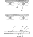
本実施例は、図6の上段にその上面から見た概略を、また図6の下段にF−F’で切っ
た断面を示すように、TFTのドレイン電極を画素領域下に延在させ、そのパターンを利
用して補助容量を形成し、さらにそのパターンが存在することで、画素電極面の凹凸を抑
制した構造としている。
In this embodiment, the drain electrode of the TFT is extended below the pixel region so as to show an outline viewed from the upper surface in the upper stage of FIG. 6 and a cross section taken along FF ′ in the lower stage of FIG. An auxiliary capacitance is formed using the pattern, and the presence of the pattern further suppresses the unevenness of the pixel electrode surface.
以下において、図1〜図6に概略の作製工程を示す。まず図1に示すようにTFTの活
性層となる領域を形成する。ここでは、TFTの活性層を非晶質珪素膜を結晶化させた結
晶性珪素膜(厚さ50nm)を利用して構成する。
In the following, schematic manufacturing steps are shown in FIGS. First, as shown in FIG. 1, a region to be an active layer of a TFT is formed. Here, the active layer of the TFT is configured using a crystalline silicon film (thickness 50 nm) obtained by crystallizing an amorphous silicon film.
ここで101、102で例示されるのがTFTの活性層パターンである。ここではTF
TとしてNチャネル型のTFTを作製する場合の例を示す。
Here, 101 and 102 are the active layer patterns of TFTs. Here TF
An example in which an N-channel TFT is manufactured as T will be described.
図1の上段に図示されるのが上面から様子である。また図1の下段に示されるのが上段
のA−A’で切った断面を示すものである。また、図1の下段において、100で示され
るのがガラス基板(または石英基板)である。
The upper part of FIG. 1 shows the state from the top. Moreover, what is shown in the lower part of FIG. 1 is a cross section cut along AA ′ in the upper part. In the lower part of FIG. 1, a glass substrate (or quartz substrate) is indicated by 100.
図1に示す状態を得たら、図2の下段に示されるようにゲイト絶縁膜として機能する酸
化珪素膜201を成膜する。ここでは、酸化珪素膜201の膜厚は100nmとする。
After obtaining the state shown in FIG. 1, a
図2において、上段のB−B’で切った断面が下段に示される断面状態図である。 FIG. 3 is a cross-sectional state diagram in which a cross section taken along B-B ′ in the upper stage is shown in the lower stage.
酸化珪素膜201を成膜したら、次にアルミウムでもってゲイト電極202を形成する
。このアルミニウム電極を構成するアルミウム膜の膜厚は、500nmとする。
After the
またこのゲイト電極の周囲表面には、陽極酸化技術を利用して陽極酸化膜203を50
nmの厚さに成膜する。この陽極酸化膜203は、ゲイト電極202を電気及び物理的に
保護する機能を有している。
An
The film is formed to a thickness of nm. The
また、ゲイト電極201は、図2の上段に示されるようにゲイト配線204から延在し
たものとして形成される。
The
図2の下段に示す状態を得たら、燐のドーピングをプラズマドーピング法でもって行い
、ソース領域207、チャネル領域206、ドレイン領域207を自己整合的に形成する
。
When the state shown in the lower part of FIG. 2 is obtained, phosphorus is doped by a plasma doping method, and the
ドーピングが終了したら、レーザー光の照射を行い、ドーピングされた燐の活性化とド
ーピング時の損傷のアニールとを行う。
When the doping is completed, laser light irradiation is performed to activate the doped phosphorus and anneal the damage during the doping.
こうして図2に示す状態を得る。次に図3に示すように層間絶縁膜として酸化珪素膜3
01をプラズマCVD法により700nmの厚さに成膜する。
In this way, the state shown in FIG. 2 is obtained. Next, as shown in FIG. 3, a silicon oxide film 3 is used as an interlayer insulating film.
01 is formed to a thickness of 700 nm by plasma CVD.
酸化珪素膜301を成膜した状態においては、ゲイト電極202の上方は盛り上がった
凸状となっている。この盛り上がりの高さは、ゲイト電極の高さ(500nm)とほぼ同
じものとなる。
In the state where the
次に50nm厚のチタン膜と400nm厚さのアルミニウム膜と50nm厚のチタン膜
をスパッタ法によって積層成膜する。そして、それをパターニングすることによって30
6、303、305のパターンを得る。(ここでは、アルミニウム膜のみのパターンを示
し、上下のチタン膜の記載は省略する)
Next, a 50 nm thick titanium film, a 400 nm thick aluminum film, and a 50 nm thick titanium film are stacked by sputtering. And 30 by patterning it
6, 303, 305 patterns are obtained. (Here, only the pattern of the aluminum film is shown, and the description of the upper and lower titanium films is omitted)
図3の306、303、305で示されるのは、パターニングされたアルミニウム膜で
ある。そしてその上下に接しているのがチタン膜である。例えば、303で示されるアル
ニウムパターンの下面にはチタン膜のパターン302が形成されており、上面にはチタン
膜のパターン304が形成されている。
なお、チタン膜を利用するのは、良好なコンタクトをとるためである。 The reason why the titanium film is used is to make a good contact.
図3の上段には、アルミニウム膜でなるパターンが示されている。(チタン膜は示され
ていない)
In the upper part of FIG. 3, a pattern made of an aluminum film is shown. (Titanium film not shown)
図3において、305、306はソース配線である。ソース配線305は、コンタクト
部307を介してTFTのソース領域に接続される。
In FIG. 3,
302、303、304の積層体パターン(ドレイン電極)はTFTのドレイン領域に
コンタクトホール308を介して接続されている。図3の上段に示されるようにこの積層
体パターンは、画素領域の大部分を示す形状を有している。
The stacked body pattern (drain electrode) of 302, 303, and 304 is connected to the drain region of the TFT through a
ここで、ゲイト電極202の膜厚は、およそ500nmである。(陽極酸化膜の成長形
態によって、厚さは多少変化する)
Here, the thickness of the
また、306、303、305のアルミニウムパターンとその上下のチタン膜の合計の
膜厚も500nmである。
The total film thickness of the
従って、多少の凹凸は形成されるが、図3の下段に示される状態において、際上面に大
きな凹凸(百nm以上に及ぶ段差を有する凹凸)は形成されない。
Accordingly, although some unevenness is formed, in the state shown in the lower part of FIG. 3, no large unevenness (unevenness having a step extending over 100 nm) is formed on the upper surface.
よって、液晶層を3μm程度としても液晶分子の乱れの影響を顕在化させない構造とす
ることができる。
Therefore, even if the liquid crystal layer has a thickness of about 3 μm, a structure that does not reveal the influence of liquid crystal molecule disturbance can be obtained.
図3に示す状態を得たら、プラズマCVD法により、窒化珪素膜400を50nmの厚
さに成膜する。(図4の下段参照)
When the state shown in FIG. 3 is obtained, a
この窒化珪素膜400は、補助容量の誘電体として機能する。また、50nmとその膜
厚を薄くするのは、その容量を極力大きくするためである。
The
次に厚さ100nmのチタン膜をスパッタリング法でもって成膜し、それをパターニン
グすることにより、補助容量形成用の電極401を形成する。
Next, a titanium film having a thickness of 100 nm is formed by a sputtering method, and patterned to form an auxiliary
この電極401は、図4の上段に示されるようにソース配線305、306に平行して
延在している。
The
なお、図4の上段のD−D’で切った断面が図4の下段に対応している。 Note that the cross section taken along D-D ′ in the upper part of FIG. 4 corresponds to the lower part of FIG. 4.
電極401とTFTのドレイン領域に接続されたドレイン電極303とは、50nm厚
の窒化珪素膜を挟んで配置され、補助容量を形成している。
The
この補助容量は、図3上段の303で示されるように大きな面積(コンタクト308の
領域は除く)でもって構成され、また窒化珪素膜400の厚さを薄くできることから、必
要とする容量を容易に確保することができる。
This auxiliary capacitance is configured with a large area (excluding the region of the contact 308) as indicated by 303 in the upper part of FIG. 3, and since the thickness of the
このことは、液晶パネルが小型化し、一つ一つの画素の面積が小さくなった場合に特に
有効なこととなる。
This is particularly effective when the liquid crystal panel is downsized and the area of each pixel is reduced.
次に図5の下段に示されるようにポリイミド樹脂でなる膜501を成膜する。膜厚は平
均で1μmとする。ポリイミド以外には、ポリアミド、ポリイミドアミド、アクリル、エ
ポキシ等の材料を利用することができる。
Next, as shown in the lower part of FIG. 5, a
このポリイミド膜によって、窒化珪素膜400の表面の凹凸やチタン膜401が存在す
ることによる凹凸が吸収される。即ち、表面のほぼ平坦なポリイミド膜501が成膜され
る。
The polyimide film absorbs unevenness on the surface of the
次にチタン膜を成膜し、さらにそれをパターニングすることにより、502で示される
チタン膜のパターンを得る。
Next, a titanium film is formed and further patterned to obtain a titanium film pattern indicated by 502.
なお、図5の上段のE−E’で切り取られる断面が図5の下段に示される。 Note that a cross section taken along E-E ′ in the upper part of FIG. 5 is shown in the lower part of FIG. 5.
この状態においては、TFTのドレイン領域のコンタクト用に開口が形成された状態と
なる。
In this state, an opening is formed for the contact of the drain region of the TFT.
チタン膜502は、その上に形成される画素電極がソース配線やTFTに電気的な干渉
を与えないようにするための電磁シールドとして設けられる。
The
図5に示す状態を得たら、図6の下段に示されるようにポリイミド樹脂膜601を平均
1.5 μmの厚さに成膜し、さらにコンタクトホールの形成を行う。そして、反射画素電極
602をアルミニウムでもって形成する。
When the state shown in FIG. 5 is obtained, the
A film is formed to a thickness of 1.5 μm, and contact holes are further formed. Then, the
この画素電極602を構成するアルミニウム膜は、スパッタ法により2000Åの厚さ
に成膜したものを利用する。
As the aluminum film constituting the
なお、図6の上段におけるF−F’で切り取られる断面を図6の下段に示す。
In addition, the cross section cut | disconnected by FF 'in the upper stage of FIG. 6 is shown in the lower stage of FIG.
この構成においては、ソース電極303が存在するために603の部分に形成されるコ
ンタクトを比較的容易に形成することができる。即ち、反射画素電極602のコンタクト
603の開口をそれ程深く形成する必要がなく、コンタクトを容易に形成することができ
る。(間口が狭く、深い開口はコンタクト不良の要因となる)
In this configuration, since the
画素電極は、格子状に配置されたソース配線及びドレイン配線の縁に一部が重なるよう
に設ける。こうすることで、開溝率を最大限高めることができる。
The pixel electrode is provided so as to partially overlap the edge of the source wiring and the drain wiring arranged in a grid pattern. By doing so, the groove opening ratio can be maximized.
図6に示す状態を得たら、配向膜としてポリイミド膜(図示せず)を120nmの厚さ
に成膜し、ラビング処理(配向処理)を施す。この際、画素電極表面の平坦性が保たれて
いるので、部分的な配向不良を抑制することができる。
When the state shown in FIG. 6 is obtained, a polyimide film (not shown) is formed to a thickness of 120 nm as an alignment film, and a rubbing process (alignment process) is performed. At this time, since the flatness of the surface of the pixel electrode is maintained, partial alignment failure can be suppressed.
あとは対向基板を用意し、対向基板との間に液晶を注入して、液晶セルを作製する。こ
うして反射型の液晶パネルが完成する。
After that, a counter substrate is prepared, and liquid crystal is injected between the counter substrate to manufacture a liquid crystal cell. A reflective liquid crystal panel is thus completed.
なお、ここでは、アクティブマトリクス回路を駆動する周辺回路については記載してい
ないが、周辺駆動回路をもTFTによって同一基板上に作製する構造とすることが好まし
い。また周辺駆動回路をICチップの外付け回路で構成するのでもよい。
Note that although a peripheral circuit for driving the active matrix circuit is not described here, it is preferable that the peripheral drive circuit is also formed on the same substrate using a TFT. Further, the peripheral drive circuit may be constituted by an external circuit of an IC chip.
本実施例に示すのは、実施例1とは異なる構造を有するTFTの例である。本実施例で
示すTFTは、図10にその上面から見た概略を示すように、活性層11がゲイト配線1
2と3カ所において交差しており、この部分にゲイト電極が配置された構造となっている
点である。
This embodiment shows an example of a TFT having a structure different from that of the first embodiment. In the TFT shown in this embodiment, the
It intersects at 2 and 3 places, and the gate electrode is arranged at this portion.
この構造は、等価的に3つのTFTが直列に接続されたものと見ることができる。 This structure can be regarded as an equivalent of three TFTs connected in series.
この構造においては、活性層の中の15の領域がソース領域、16の領域がドレイン領
域として定義される。
In this structure, 15 regions in the active layer are defined as source regions and 16 regions are defined as drain regions.
図10には、ソース配線13とソース配線と同時に形成されるドレイン電極14が示さ
れている。
FIG. 10 shows the
ドレイン電極14は、画素電極内の大部分を占めるようにそのパターンが形成されてい
る。ドレイン電極14は、図3のパターン303に対応する。
The pattern of the
このドレイン電極14は、
(1)補助容量の形成
(2)画素電極の平坦化
(3)画素電極のコンタクト形成を容易にする。
といった役割を有している。
The
(1) Formation of auxiliary capacitance (2) Flattening of pixel electrode (3) Facilitation of pixel electrode contact formation
Has the role.
図10に示すような構造は、活性層11中に3つのチャネルが形成され、各チャネルに
は、ソース配線と画素電極との間に加わる電圧を3分圧したものが加わることになる。こ
うすることで、TFTの耐圧を高めることができる。
In the structure shown in FIG. 10, three channels are formed in the
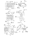
本実施例では、発明を利用して得られた反射型の液晶パネルを利用した表示装置の例を
示す。
In this embodiment, an example of a display device using a reflective liquid crystal panel obtained by using the invention will be described.
図9(A)に示すのは、携帯型の情報処理端末であり、電話回線を利用した通信機能を
有している。
FIG. 9A shows a portable information processing terminal, which has a communication function using a telephone line.
この電子装置は、集積化回路2006を本体2001の内部に備えている。そして、T
FTをスイッチング素子として配置した反射型のアクティブマトリクス型の液晶パネル2
005、画像を取り込むカメラ部2002、さらに操作スイッチ2004を備えている。
This electronic device includes an integrated circuit 2006 inside a main body 2001. And T
Reflective active matrix liquid crystal panel 2 in which FT is arranged as a switching element
005, a camera unit 2002 for capturing an image, and an operation switch 2004 are provided.
図9(B)に示すのは、ヘッドマウントディスプレイと呼ばれる電子装置である。この
装置は、バンド2103によって頭に本体21201を装着して、疑似的に目の前に画像
を表示する機能を有している。画像は、左右の目に対応した反射型のアクティブマトクス
型の液晶パネル2102によって構成される。
FIG. 9B illustrates an electronic device called a head mounted display. This apparatus has a function of displaying an image in front of the eyes by wearing a main body 21201 on the head with a
図9(C)に示すのは、人工衛星からの信号を基に地図情報や各種情報を表示する機能
を有している。アンテナ2204で捉えた衛星からの情報は、本体2201内部に備えた
電子回路で処理され、アクティブマトリクス型の反射型の液晶パネル2202に必要な情
報が表示される。
FIG. 9C has a function of displaying map information and various information based on a signal from an artificial satellite. Information from the satellite captured by the
装置の操作は、操作スイッチ2203によって行われる。このような装置においてもT
FTを利用した回路が利用される。
The operation of the apparatus is performed by an
A circuit using FT is used.
図9(D)に示すのは、携帯電話である。この電子装置は、本体2301にアンテナ2
306、音声出力部2302、液晶パネル2304、操作スイッチ2305、音声入力部
2303を備えている。
FIG. 9D illustrates a mobile phone. This electronic device includes a main body 2301 and an antenna 2.
306, an audio output unit 2302, a liquid crystal panel 2304, operation switches 2305, and an audio input unit 2303.
図9(E)に示す電子装置は、ビデオカメラと称される携帯型の撮像装置である。この
電子装置は、本体2401に開閉部材に取り付けられた反射型の液晶パネル2402、開
閉部材に取り付けられた操作スイッチ2404を備えている。
An electronic device illustrated in FIG. 9E is a portable imaging device called a video camera. This electronic apparatus includes a reflection type liquid crystal panel 2402 attached to an opening / closing member and an
さらにまた、本体2401には、画像の受像部2406、集積化回路2407、音声入
力部2403、操作スイッチ2404、バッテリー2405が備えられている。
Further, the main body 2401 includes an image receiving unit 2406, an
図9(F)に示す電子装置は、投射型の液晶表示装置である。この装置は、本体250
1に光源2502、反射型の液晶パネル2503、光学系2504備え、スクリンー25
05に画像を投影する機能を有している。
The electronic device illustrated in FIG. 9F is a projection liquid crystal display device. This device has a main body 250.
1 includes a
05 has a function of projecting an image.
なお、本明細書で開示する発明は、液晶を利用する場合の以外のフラットパネルディス
プレイにも利用することができる。例えば、ELディスプレイであれば、発光層の下地を
平坦化する場合に利用することができる。またECディスプレイ等にも利用することがで
きる。
Note that the invention disclosed in this specification can be used for flat panel displays other than the case of using liquid crystal. For example, in the case of an EL display, it can be used when the base of the light emitting layer is flattened. It can also be used for EC displays.
即ち、本明細書で開示する発明は、画素領域の上方の表面を平坦にしたい構造を実現す
るために利用することができる。
That is, the invention disclosed in this specification can be used to realize a structure in which the surface above the pixel region is desired to be flat.
101、102 TFTの活性層
100 ガラス基板(または石英基板)
201 ゲイト絶縁膜
202 ゲイト電極(アルミニウムで構成される)
203 陽極酸化膜
204 ゲイト配線
301 層間絶縁膜(酸化珪素膜)
302 ドレイン電極(チタン膜)
303 ドレイン電極(アルミニウム膜)
304 ドレイン電極(チタン膜)
305 ソース配線(ソース電極)
306 ソース配線(ソース電極)
307 ソースコンタクト部
308 ドレインコンタクト部
400 窒化珪素膜
401 容量形成用の電極
501 層間絶縁膜(ポリイミド樹脂膜)
502 電界遮蔽用シールド(ブラックマトリクス)
601 層間絶縁膜(ポリイミド樹脂膜)
602 画素電極(アルミニウム膜)
603 画素コンタクト部
101, 102 Active layer of
201
203
302 Drain electrode (titanium film)
303 Drain electrode (aluminum film)
304 Drain electrode (titanium film)
305 Source wiring (source electrode)
306 Source wiring (source electrode)
307
502 Shield for electric field shielding (black matrix)
601 Interlayer insulation film (polyimide resin film)
602 Pixel electrode (aluminum film)
603 Pixel contact portion
Claims (1)
前記ソース配線にソース領域が接続され、前記ゲイト配線がゲイト電極に接続された薄膜トランジスタと、
前記ソース配線と同時に形成されたドレイン電極と、前記ドレイン電極の上方に形成された補助容量用電極と、
前記補助容量用電極の上方に形成された反射画素電極と、を有し、
前記ドレイン電極と前記補助容量用電極との間には補助容量が形成され、
前記ドレイン電極は画素領域の大部分を占めていることを特徴とする表示装置。 Source wiring and gate wiring arranged in a grid,
A thin film transistor in which a source region is connected to the source wiring and the gate wiring is connected to a gate electrode;
A drain electrode formed simultaneously with the source wiring, an auxiliary capacitance electrode formed above the drain electrode,
A reflective pixel electrode formed above the auxiliary capacitance electrode,
A storage capacitor is formed between the drain electrode and the storage capacitor electrode,
The display device, wherein the drain electrode occupies most of a pixel region.
Priority Applications (1)
| Application Number | Priority Date | Filing Date | Title |
|---|---|---|---|
| JP2012188685A JP2012252361A (en) | 2012-08-29 | 2012-08-29 | Display device |
Applications Claiming Priority (1)
| Application Number | Priority Date | Filing Date | Title |
|---|---|---|---|
| JP2012188685A JP2012252361A (en) | 2012-08-29 | 2012-08-29 | Display device |
Related Parent Applications (1)
| Application Number | Title | Priority Date | Filing Date |
|---|---|---|---|
| JP2009132274A Division JP2009193081A (en) | 2009-06-01 | 2009-06-01 | Display and electronic device |
Related Child Applications (1)
| Application Number | Title | Priority Date | Filing Date |
|---|---|---|---|
| JP2013266273A Division JP5941455B2 (en) | 2013-12-25 | 2013-12-25 | Display device |
Publications (1)
| Publication Number | Publication Date |
|---|---|
| JP2012252361A true JP2012252361A (en) | 2012-12-20 |
Family
ID=47525163
Family Applications (1)
| Application Number | Title | Priority Date | Filing Date |
|---|---|---|---|
| JP2012188685A Withdrawn JP2012252361A (en) | 2012-08-29 | 2012-08-29 | Display device |
Country Status (1)
| Country | Link |
|---|---|
| JP (1) | JP2012252361A (en) |
Citations (3)
| Publication number | Priority date | Publication date | Assignee | Title |
|---|---|---|---|---|
| JPH032839A (en) * | 1989-05-31 | 1991-01-09 | Matsushita Electric Ind Co Ltd | Reflection type liquid crystal light valve element |
| JPH03185428A (en) * | 1989-12-15 | 1991-08-13 | Seiko Epson Corp | Liquid crystal display device |
| JPH07181517A (en) * | 1993-12-22 | 1995-07-21 | Toshiba Corp | Active matrix type liquid crystal display device |
-
2012
- 2012-08-29 JP JP2012188685A patent/JP2012252361A/en not_active Withdrawn
Patent Citations (3)
| Publication number | Priority date | Publication date | Assignee | Title |
|---|---|---|---|---|
| JPH032839A (en) * | 1989-05-31 | 1991-01-09 | Matsushita Electric Ind Co Ltd | Reflection type liquid crystal light valve element |
| JPH03185428A (en) * | 1989-12-15 | 1991-08-13 | Seiko Epson Corp | Liquid crystal display device |
| JPH07181517A (en) * | 1993-12-22 | 1995-07-21 | Toshiba Corp | Active matrix type liquid crystal display device |
Similar Documents
| Publication | Publication Date | Title |
|---|---|---|
| JP3871764B2 (en) | Reflective display device | |
| US10203576B2 (en) | Display substrate with a common electrode and liquid crystal display panel having the same | |
| US10777887B2 (en) | Scanning antenna and method for manufacturing same | |
| US10756409B2 (en) | Scanning antenna and method for manufacturing same | |
| US7663723B2 (en) | In-plane switching mode liquid crystal display device and fabrication method thereof | |
| JP5638833B2 (en) | Image display device and manufacturing method thereof | |
| US9853164B2 (en) | Semiconductor device and display device | |
| US10276595B2 (en) | Liquid crystal display device and method of manufacturing a liquid crystal display device | |
| KR20140129504A (en) | Array substrate for fringe field switching mode liquid crystal display device | |
| KR20130015737A (en) | Liquid crystal display device | |
| US10026374B2 (en) | Liquid crystal display apparatus | |
| JP2007293155A (en) | Liquid crystal display device | |
| US9835900B2 (en) | Display device | |
| US8665413B2 (en) | Thin film transistor array panel, liquid crystal display, and manufacturing method thereof | |
| US9703152B2 (en) | Liquid crystal display device | |
| JP2017111388A (en) | Liquid crystal display device | |
| JP4294669B2 (en) | Display device | |
| JP4294664B2 (en) | Display device | |
| JP2007093859A (en) | Liquid crystal device and electronic apparatus | |
| JP2007004204A (en) | Display device | |
| JP5941455B2 (en) | Display device | |
| JP2012252361A (en) | Display device | |
| JP2009193081A (en) | Display and electronic device | |
| US10534229B2 (en) | Liquid crystal display device and method of manufacturing the same | |
| JP5525705B2 (en) | Liquid crystal display |
Legal Events
| Date | Code | Title | Description |
|---|---|---|---|
| A977 | Report on retrieval |
Free format text: JAPANESE INTERMEDIATE CODE: A971007 Effective date: 20130522 |
|
| A131 | Notification of reasons for refusal |
Free format text: JAPANESE INTERMEDIATE CODE: A131 Effective date: 20130529 |
|
| A02 | Decision of refusal |
Free format text: JAPANESE INTERMEDIATE CODE: A02 Effective date: 20131001 |
|
| A761 | Written withdrawal of application |
Free format text: JAPANESE INTERMEDIATE CODE: A761 Effective date: 20131227 |