JP2012248696A - Organic electroluminescent element - Google Patents
Organic electroluminescent element Download PDFInfo
- Publication number
- JP2012248696A JP2012248696A JP2011119538A JP2011119538A JP2012248696A JP 2012248696 A JP2012248696 A JP 2012248696A JP 2011119538 A JP2011119538 A JP 2011119538A JP 2011119538 A JP2011119538 A JP 2011119538A JP 2012248696 A JP2012248696 A JP 2012248696A
- Authority
- JP
- Japan
- Prior art keywords
- light emitting
- light
- layer
- emitting layer
- electrode
- Prior art date
- Legal status (The legal status is an assumption and is not a legal conclusion. Google has not performed a legal analysis and makes no representation as to the accuracy of the status listed.)
- Withdrawn
Links
- 239000010410 layer Substances 0.000 claims abstract description 160
- 239000002245 particle Substances 0.000 claims abstract description 57
- 239000000463 material Substances 0.000 claims abstract description 46
- 239000000758 substrate Substances 0.000 claims abstract description 40
- 238000005401 electroluminescence Methods 0.000 claims abstract description 25
- 239000012044 organic layer Substances 0.000 claims abstract description 17
- 238000010030 laminating Methods 0.000 claims abstract description 5
- 238000000605 extraction Methods 0.000 abstract description 9
- VYPSYNLAJGMNEJ-UHFFFAOYSA-N Silicium dioxide Chemical compound O=[Si]=O VYPSYNLAJGMNEJ-UHFFFAOYSA-N 0.000 description 66
- 239000000377 silicon dioxide Substances 0.000 description 33
- 230000005525 hole transport Effects 0.000 description 28
- 239000010419 fine particle Substances 0.000 description 21
- 238000002347 injection Methods 0.000 description 21
- 239000007924 injection Substances 0.000 description 21
- 239000012298 atmosphere Substances 0.000 description 15
- KFZMGEQAYNKOFK-UHFFFAOYSA-N Isopropanol Chemical compound CC(C)O KFZMGEQAYNKOFK-UHFFFAOYSA-N 0.000 description 12
- -1 hexoxy-phenylene vinylene Chemical group 0.000 description 12
- 239000004094 surface-active agent Substances 0.000 description 12
- 229920000642 polymer Polymers 0.000 description 11
- 229910052782 aluminium Inorganic materials 0.000 description 10
- 239000011521 glass Substances 0.000 description 10
- 229910052751 metal Inorganic materials 0.000 description 10
- 239000002184 metal Substances 0.000 description 10
- LFQSCWFLJHTTHZ-UHFFFAOYSA-N Ethanol Chemical compound CCO LFQSCWFLJHTTHZ-UHFFFAOYSA-N 0.000 description 8
- 239000002131 composite material Substances 0.000 description 8
- 239000000203 mixture Substances 0.000 description 8
- 239000000243 solution Substances 0.000 description 8
- 238000000034 method Methods 0.000 description 7
- 238000007789 sealing Methods 0.000 description 7
- 239000000126 substance Substances 0.000 description 7
- LYCAIKOWRPUZTN-UHFFFAOYSA-N Ethylene glycol Chemical compound OCCO LYCAIKOWRPUZTN-UHFFFAOYSA-N 0.000 description 6
- LRHPLDYGYMQRHN-UHFFFAOYSA-N N-Butanol Chemical compound CCCCO LRHPLDYGYMQRHN-UHFFFAOYSA-N 0.000 description 6
- 150000001875 compounds Chemical class 0.000 description 6
- 229910052709 silver Inorganic materials 0.000 description 6
- 239000002904 solvent Substances 0.000 description 6
- LZZYPRNAOMGNLH-UHFFFAOYSA-M Cetrimonium bromide Chemical compound [Br-].CCCCCCCCCCCCCCCC[N+](C)(C)C LZZYPRNAOMGNLH-UHFFFAOYSA-M 0.000 description 5
- 230000000052 comparative effect Effects 0.000 description 5
- 239000000975 dye Substances 0.000 description 5
- AUHZEENZYGFFBQ-UHFFFAOYSA-N 1,3,5-trimethylbenzene Chemical compound CC1=CC(C)=CC(C)=C1 AUHZEENZYGFFBQ-UHFFFAOYSA-N 0.000 description 4
- 229910004298 SiO 2 Inorganic materials 0.000 description 4
- ZSWFCLXCOIISFI-UHFFFAOYSA-N cyclopentadiene Chemical compound C1C=CC=C1 ZSWFCLXCOIISFI-UHFFFAOYSA-N 0.000 description 4
- 239000011368 organic material Substances 0.000 description 4
- 229920000767 polyaniline Polymers 0.000 description 4
- 239000011347 resin Substances 0.000 description 4
- 229920005989 resin Polymers 0.000 description 4
- 239000007983 Tris buffer Substances 0.000 description 3
- XLOMVQKBTHCTTD-UHFFFAOYSA-N Zinc monoxide Chemical compound [Zn]=O XLOMVQKBTHCTTD-UHFFFAOYSA-N 0.000 description 3
- 229920000109 alkoxy-substituted poly(p-phenylene vinylene) Polymers 0.000 description 3
- XAGFODPZIPBFFR-UHFFFAOYSA-N aluminium Chemical compound [Al] XAGFODPZIPBFFR-UHFFFAOYSA-N 0.000 description 3
- 239000003795 chemical substances by application Substances 0.000 description 3
- AMGQUBHHOARCQH-UHFFFAOYSA-N indium;oxotin Chemical compound [In].[Sn]=O AMGQUBHHOARCQH-UHFFFAOYSA-N 0.000 description 3
- 239000007788 liquid Substances 0.000 description 3
- 238000004519 manufacturing process Methods 0.000 description 3
- 150000002736 metal compounds Chemical class 0.000 description 3
- 229910044991 metal oxide Inorganic materials 0.000 description 3
- 150000004706 metal oxides Chemical class 0.000 description 3
- 230000003287 optical effect Effects 0.000 description 3
- 229920003023 plastic Polymers 0.000 description 3
- YVTHLONGBIQYBO-UHFFFAOYSA-N zinc indium(3+) oxygen(2-) Chemical compound [O--].[Zn++].[In+3] YVTHLONGBIQYBO-UHFFFAOYSA-N 0.000 description 3
- WYTZZXDRDKSJID-UHFFFAOYSA-N (3-aminopropyl)triethoxysilane Chemical compound CCO[Si](OCC)(OCC)CCCN WYTZZXDRDKSJID-UHFFFAOYSA-N 0.000 description 2
- GOLORTLGFDVFDW-UHFFFAOYSA-N 3-(1h-benzimidazol-2-yl)-7-(diethylamino)chromen-2-one Chemical compound C1=CC=C2NC(C3=CC4=CC=C(C=C4OC3=O)N(CC)CC)=NC2=C1 GOLORTLGFDVFDW-UHFFFAOYSA-N 0.000 description 2
- 239000004925 Acrylic resin Substances 0.000 description 2
- 229920000178 Acrylic resin Polymers 0.000 description 2
- VTYYLEPIZMXCLO-UHFFFAOYSA-L Calcium carbonate Chemical compound [Ca+2].[O-]C([O-])=O VTYYLEPIZMXCLO-UHFFFAOYSA-L 0.000 description 2
- UFWIBTONFRDIAS-UHFFFAOYSA-N Naphthalene Chemical compound C1=CC=CC2=CC=CC=C21 UFWIBTONFRDIAS-UHFFFAOYSA-N 0.000 description 2
- 239000004952 Polyamide Substances 0.000 description 2
- 239000004695 Polyether sulfone Substances 0.000 description 2
- 239000004698 Polyethylene Substances 0.000 description 2
- 239000004743 Polypropylene Substances 0.000 description 2
- 239000004793 Polystyrene Substances 0.000 description 2
- 229920001328 Polyvinylidene chloride Polymers 0.000 description 2
- BOTDANWDWHJENH-UHFFFAOYSA-N Tetraethyl orthosilicate Chemical compound CCO[Si](OCC)(OCC)OCC BOTDANWDWHJENH-UHFFFAOYSA-N 0.000 description 2
- 239000000654 additive Substances 0.000 description 2
- 230000000996 additive effect Effects 0.000 description 2
- 239000003513 alkali Substances 0.000 description 2
- MWPLVEDNUUSJAV-UHFFFAOYSA-N anthracene Chemical compound C1=CC=CC2=CC3=CC=CC=C3C=C21 MWPLVEDNUUSJAV-UHFFFAOYSA-N 0.000 description 2
- 239000007864 aqueous solution Substances 0.000 description 2
- 230000004888 barrier function Effects 0.000 description 2
- 239000011575 calcium Substances 0.000 description 2
- 239000004020 conductor Substances 0.000 description 2
- VPUGDVKSAQVFFS-UHFFFAOYSA-N coronene Chemical compound C1=C(C2=C34)C=CC3=CC=C(C=C3)C4=C4C3=CC=C(C=C3)C4=C2C3=C1 VPUGDVKSAQVFFS-UHFFFAOYSA-N 0.000 description 2
- 239000013078 crystal Substances 0.000 description 2
- DMBHHRLKUKUOEG-UHFFFAOYSA-N diphenylamine Chemical compound C=1C=CC=CC=1NC1=CC=CC=C1 DMBHHRLKUKUOEG-UHFFFAOYSA-N 0.000 description 2
- 239000007772 electrode material Substances 0.000 description 2
- 238000011156 evaluation Methods 0.000 description 2
- 239000007789 gas Substances 0.000 description 2
- PCHJSUWPFVWCPO-UHFFFAOYSA-N gold Chemical compound [Au] PCHJSUWPFVWCPO-UHFFFAOYSA-N 0.000 description 2
- 229910052737 gold Inorganic materials 0.000 description 2
- 239000010931 gold Substances 0.000 description 2
- UQEAIHBTYFGYIE-UHFFFAOYSA-N hexamethyldisiloxane Chemical compound C[Si](C)(C)O[Si](C)(C)C UQEAIHBTYFGYIE-UHFFFAOYSA-N 0.000 description 2
- 230000002209 hydrophobic effect Effects 0.000 description 2
- 229910003437 indium oxide Inorganic materials 0.000 description 2
- PJXISJQVUVHSOJ-UHFFFAOYSA-N indium(iii) oxide Chemical compound [O-2].[O-2].[O-2].[In+3].[In+3] PJXISJQVUVHSOJ-UHFFFAOYSA-N 0.000 description 2
- 238000003475 lamination Methods 0.000 description 2
- 239000002082 metal nanoparticle Substances 0.000 description 2
- 150000002739 metals Chemical class 0.000 description 2
- 239000002070 nanowire Substances 0.000 description 2
- 125000001997 phenyl group Chemical group [H]C1=C([H])C([H])=C(*)C([H])=C1[H] 0.000 description 2
- 229920003229 poly(methyl methacrylate) Polymers 0.000 description 2
- 229920002647 polyamide Polymers 0.000 description 2
- 229920001230 polyarylate Polymers 0.000 description 2
- 229920005668 polycarbonate resin Polymers 0.000 description 2
- 239000004431 polycarbonate resin Substances 0.000 description 2
- 229920006393 polyether sulfone Polymers 0.000 description 2
- 229920000573 polyethylene Polymers 0.000 description 2
- 239000005020 polyethylene terephthalate Substances 0.000 description 2
- 229920000139 polyethylene terephthalate Polymers 0.000 description 2
- 239000004926 polymethyl methacrylate Substances 0.000 description 2
- 229920001155 polypropylene Polymers 0.000 description 2
- 229920002223 polystyrene Polymers 0.000 description 2
- 229920002635 polyurethane Polymers 0.000 description 2
- 239000004814 polyurethane Substances 0.000 description 2
- 239000011118 polyvinyl acetate Substances 0.000 description 2
- 229920002689 polyvinyl acetate Polymers 0.000 description 2
- 229920000915 polyvinyl chloride Polymers 0.000 description 2
- 239000004800 polyvinyl chloride Substances 0.000 description 2
- 239000005033 polyvinylidene chloride Substances 0.000 description 2
- BBEAQIROQSPTKN-UHFFFAOYSA-N pyrene Chemical compound C1=CC=C2C=CC3=CC=CC4=CC=C1C2=C43 BBEAQIROQSPTKN-UHFFFAOYSA-N 0.000 description 2
- 239000007790 solid phase Substances 0.000 description 2
- 238000005507 spraying Methods 0.000 description 2
- 238000004544 sputter deposition Methods 0.000 description 2
- 238000003756 stirring Methods 0.000 description 2
- XOLBLPGZBRYERU-UHFFFAOYSA-N tin dioxide Chemical compound O=[Sn]=O XOLBLPGZBRYERU-UHFFFAOYSA-N 0.000 description 2
- 229910001887 tin oxide Inorganic materials 0.000 description 2
- 238000006227 trimethylsilylation reaction Methods 0.000 description 2
- 238000001771 vacuum deposition Methods 0.000 description 2
- XLYOFNOQVPJJNP-UHFFFAOYSA-N water Substances O XLYOFNOQVPJJNP-UHFFFAOYSA-N 0.000 description 2
- 239000011787 zinc oxide Substances 0.000 description 2
- UWRZIZXBOLBCON-VOTSOKGWSA-N (e)-2-phenylethenamine Chemical class N\C=C\C1=CC=CC=C1 UWRZIZXBOLBCON-VOTSOKGWSA-N 0.000 description 1
- NGQSLSMAEVWNPU-YTEMWHBBSA-N 1,2-bis[(e)-2-phenylethenyl]benzene Chemical class C=1C=CC=CC=1/C=C/C1=CC=CC=C1\C=C\C1=CC=CC=C1 NGQSLSMAEVWNPU-YTEMWHBBSA-N 0.000 description 1
- KLCLIOISYBHYDZ-UHFFFAOYSA-N 1,4,4-triphenylbuta-1,3-dienylbenzene Chemical compound C=1C=CC=CC=1C(C=1C=CC=CC=1)=CC=C(C=1C=CC=CC=1)C1=CC=CC=C1 KLCLIOISYBHYDZ-UHFFFAOYSA-N 0.000 description 1
- GUPMCMZMDAGSPF-UHFFFAOYSA-N 1-phenylbuta-1,3-dienylbenzene Chemical compound C=1C=CC=CC=1[C](C=C[CH2])C1=CC=CC=C1 GUPMCMZMDAGSPF-UHFFFAOYSA-N 0.000 description 1
- MGADZUXDNSDTHW-UHFFFAOYSA-N 2H-pyran Chemical compound C1OC=CC=C1 MGADZUXDNSDTHW-UHFFFAOYSA-N 0.000 description 1
- 229910018072 Al 2 O 3 Inorganic materials 0.000 description 1
- 229910001148 Al-Li alloy Inorganic materials 0.000 description 1
- OYPRJOBELJOOCE-UHFFFAOYSA-N Calcium Chemical compound [Ca] OYPRJOBELJOOCE-UHFFFAOYSA-N 0.000 description 1
- 150000000918 Europium Chemical class 0.000 description 1
- 229910001111 Fine metal Inorganic materials 0.000 description 1
- YCKRFDGAMUMZLT-UHFFFAOYSA-N Fluorine atom Chemical compound [F] YCKRFDGAMUMZLT-UHFFFAOYSA-N 0.000 description 1
- VEXZGXHMUGYJMC-UHFFFAOYSA-N Hydrochloric acid Chemical compound Cl VEXZGXHMUGYJMC-UHFFFAOYSA-N 0.000 description 1
- DGAQECJNVWCQMB-PUAWFVPOSA-M Ilexoside XXIX Chemical compound C[C@@H]1CC[C@@]2(CC[C@@]3(C(=CC[C@H]4[C@]3(CC[C@@H]5[C@@]4(CC[C@@H](C5(C)C)OS(=O)(=O)[O-])C)C)[C@@H]2[C@]1(C)O)C)C(=O)O[C@H]6[C@@H]([C@H]([C@@H]([C@H](O6)CO)O)O)O.[Na+] DGAQECJNVWCQMB-PUAWFVPOSA-M 0.000 description 1
- 229910000799 K alloy Inorganic materials 0.000 description 1
- WHXSMMKQMYFTQS-UHFFFAOYSA-N Lithium Chemical compound [Li] WHXSMMKQMYFTQS-UHFFFAOYSA-N 0.000 description 1
- FYYHWMGAXLPEAU-UHFFFAOYSA-N Magnesium Chemical compound [Mg] FYYHWMGAXLPEAU-UHFFFAOYSA-N 0.000 description 1
- MUBZPKHOEPUJKR-UHFFFAOYSA-N Oxalic acid Chemical compound OC(=O)C(O)=O MUBZPKHOEPUJKR-UHFFFAOYSA-N 0.000 description 1
- 229920000144 PEDOT:PSS Polymers 0.000 description 1
- 229920001609 Poly(3,4-ethylenedioxythiophene) Polymers 0.000 description 1
- 239000004642 Polyimide Substances 0.000 description 1
- WTKZEGDFNFYCGP-UHFFFAOYSA-N Pyrazole Chemical compound C=1C=NNC=1 WTKZEGDFNFYCGP-UHFFFAOYSA-N 0.000 description 1
- NRCMAYZCPIVABH-UHFFFAOYSA-N Quinacridone Chemical compound N1C2=CC=CC=C2C(=O)C2=C1C=C1C(=O)C3=CC=CC=C3NC1=C2 NRCMAYZCPIVABH-UHFFFAOYSA-N 0.000 description 1
- 229910006404 SnO 2 Inorganic materials 0.000 description 1
- CDBYLPFSWZWCQE-UHFFFAOYSA-L Sodium Carbonate Chemical compound [Na+].[Na+].[O-]C([O-])=O CDBYLPFSWZWCQE-UHFFFAOYSA-L 0.000 description 1
- XBDYBAVJXHJMNQ-UHFFFAOYSA-N Tetrahydroanthracene Natural products C1=CC=C2C=C(CCCC3)C3=CC2=C1 XBDYBAVJXHJMNQ-UHFFFAOYSA-N 0.000 description 1
- JFBZPFYRPYOZCQ-UHFFFAOYSA-N [Li].[Al] Chemical compound [Li].[Al] JFBZPFYRPYOZCQ-UHFFFAOYSA-N 0.000 description 1
- JHYLKGDXMUDNEO-UHFFFAOYSA-N [Mg].[In] Chemical compound [Mg].[In] JHYLKGDXMUDNEO-UHFFFAOYSA-N 0.000 description 1
- 239000006096 absorbing agent Substances 0.000 description 1
- DHKHKXVYLBGOIT-UHFFFAOYSA-N acetaldehyde Diethyl Acetal Natural products CCOC(C)OCC DHKHKXVYLBGOIT-UHFFFAOYSA-N 0.000 description 1
- 125000002777 acetyl group Chemical class [H]C([H])([H])C(*)=O 0.000 description 1
- 229910052783 alkali metal Inorganic materials 0.000 description 1
- 229910001508 alkali metal halide Inorganic materials 0.000 description 1
- 150000008045 alkali metal halides Chemical class 0.000 description 1
- 229910000272 alkali metal oxide Inorganic materials 0.000 description 1
- 150000001340 alkali metals Chemical class 0.000 description 1
- 229910045601 alloy Inorganic materials 0.000 description 1
- 239000000956 alloy Substances 0.000 description 1
- 150000001412 amines Chemical class 0.000 description 1
- SMWDFEZZVXVKRB-UHFFFAOYSA-N anhydrous quinoline Natural products N1=CC=CC2=CC=CC=C21 SMWDFEZZVXVKRB-UHFFFAOYSA-N 0.000 description 1
- 229910052788 barium Inorganic materials 0.000 description 1
- DSAJWYNOEDNPEQ-UHFFFAOYSA-N barium atom Chemical compound [Ba] DSAJWYNOEDNPEQ-UHFFFAOYSA-N 0.000 description 1
- WZJYKHNJTSNBHV-UHFFFAOYSA-N benzoquinoline Natural products C1=CN=C2C3=CC=CC=C3C=CC2=C1 WZJYKHNJTSNBHV-UHFFFAOYSA-N 0.000 description 1
- 230000005540 biological transmission Effects 0.000 description 1
- 230000015572 biosynthetic process Effects 0.000 description 1
- 229910052791 calcium Inorganic materials 0.000 description 1
- 229910000019 calcium carbonate Inorganic materials 0.000 description 1
- 238000005266 casting Methods 0.000 description 1
- 239000012461 cellulose resin Substances 0.000 description 1
- 238000005119 centrifugation Methods 0.000 description 1
- 238000006243 chemical reaction Methods 0.000 description 1
- 239000012295 chemical reaction liquid Substances 0.000 description 1
- 239000011248 coating agent Substances 0.000 description 1
- 238000000576 coating method Methods 0.000 description 1
- 229920001940 conductive polymer Polymers 0.000 description 1
- 229920001577 copolymer Polymers 0.000 description 1
- 238000007607 die coating method Methods 0.000 description 1
- 238000003618 dip coating Methods 0.000 description 1
- 239000006185 dispersion Substances 0.000 description 1
- 238000009826 distribution Methods 0.000 description 1
- 239000002019 doping agent Substances 0.000 description 1
- 230000001747 exhibiting effect Effects 0.000 description 1
- GVEPBJHOBDJJJI-UHFFFAOYSA-N fluoranthrene Natural products C1=CC(C2=CC=CC=C22)=C3C2=CC=CC3=C1 GVEPBJHOBDJJJI-UHFFFAOYSA-N 0.000 description 1
- 239000007850 fluorescent dye Substances 0.000 description 1
- 239000011737 fluorine Substances 0.000 description 1
- 229910052731 fluorine Inorganic materials 0.000 description 1
- 239000011888 foil Substances 0.000 description 1
- 238000007756 gravure coating Methods 0.000 description 1
- 230000001678 irradiating effect Effects 0.000 description 1
- 229910052744 lithium Inorganic materials 0.000 description 1
- 239000001989 lithium alloy Substances 0.000 description 1
- 238000004020 luminiscence type Methods 0.000 description 1
- 229910052749 magnesium Inorganic materials 0.000 description 1
- 239000011777 magnesium Substances 0.000 description 1
- ORUIBWPALBXDOA-UHFFFAOYSA-L magnesium fluoride Chemical compound [F-].[F-].[Mg+2] ORUIBWPALBXDOA-UHFFFAOYSA-L 0.000 description 1
- 229910001635 magnesium fluoride Inorganic materials 0.000 description 1
- SJCKRGFTWFGHGZ-UHFFFAOYSA-N magnesium silver Chemical compound [Mg].[Ag] SJCKRGFTWFGHGZ-UHFFFAOYSA-N 0.000 description 1
- 239000002923 metal particle Substances 0.000 description 1
- 238000002156 mixing Methods 0.000 description 1
- 239000000178 monomer Substances 0.000 description 1
- 239000012299 nitrogen atmosphere Substances 0.000 description 1
- WCPAKWJPBJAGKN-UHFFFAOYSA-N oxadiazole Chemical compound C1=CON=N1 WCPAKWJPBJAGKN-UHFFFAOYSA-N 0.000 description 1
- 125000002080 perylenyl group Chemical group C1(=CC=C2C=CC=C3C4=CC=CC5=CC=CC(C1=C23)=C45)* 0.000 description 1
- CSHWQDPOILHKBI-UHFFFAOYSA-N peryrene Natural products C1=CC(C2=CC=CC=3C2=C2C=CC=3)=C3C2=CC=CC3=C1 CSHWQDPOILHKBI-UHFFFAOYSA-N 0.000 description 1
- XNGIFLGASWRNHJ-UHFFFAOYSA-L phthalate(2-) Chemical compound [O-]C(=O)C1=CC=CC=C1C([O-])=O XNGIFLGASWRNHJ-UHFFFAOYSA-L 0.000 description 1
- 229920000172 poly(styrenesulfonic acid) Polymers 0.000 description 1
- 229920002239 polyacrylonitrile Polymers 0.000 description 1
- 239000004417 polycarbonate Substances 0.000 description 1
- 229920000515 polycarbonate Polymers 0.000 description 1
- 229920002098 polyfluorene Chemical class 0.000 description 1
- 229920001721 polyimide Polymers 0.000 description 1
- 229940005642 polystyrene sulfonic acid Drugs 0.000 description 1
- 239000011148 porous material Substances 0.000 description 1
- BITYAPCSNKJESK-UHFFFAOYSA-N potassiosodium Chemical compound [Na].[K] BITYAPCSNKJESK-UHFFFAOYSA-N 0.000 description 1
- 238000002360 preparation method Methods 0.000 description 1
- 230000001902 propagating effect Effects 0.000 description 1
- 229910052761 rare earth metal Inorganic materials 0.000 description 1
- 150000002910 rare earth metals Chemical class 0.000 description 1
- 238000010992 reflux Methods 0.000 description 1
- YYMBJDOZVAITBP-UHFFFAOYSA-N rubrene Chemical compound C1=CC=CC=C1C(C1=C(C=2C=CC=CC=2)C2=CC=CC=C2C(C=2C=CC=CC=2)=C11)=C(C=CC=C2)C2=C1C1=CC=CC=C1 YYMBJDOZVAITBP-UHFFFAOYSA-N 0.000 description 1
- 238000000790 scattering method Methods 0.000 description 1
- 238000007650 screen-printing Methods 0.000 description 1
- 239000004332 silver Substances 0.000 description 1
- 239000005361 soda-lime glass Substances 0.000 description 1
- 229910052708 sodium Inorganic materials 0.000 description 1
- 239000011734 sodium Substances 0.000 description 1
- 238000004528 spin coating Methods 0.000 description 1
- IFLREYGFSNHWGE-UHFFFAOYSA-N tetracene Chemical compound C1=CC=CC2=CC3=CC4=CC=CC=C4C=C3C=C21 IFLREYGFSNHWGE-UHFFFAOYSA-N 0.000 description 1
- 229920005992 thermoplastic resin Polymers 0.000 description 1
- 239000012780 transparent material Substances 0.000 description 1
- 229920002554 vinyl polymer Polymers 0.000 description 1
- 239000011800 void material Substances 0.000 description 1
Images

Landscapes
- Electroluminescent Light Sources (AREA)
Abstract
【課題】光取出し量を増加させるとともに、ダークスポットの発生を抑えた有機エレクトロルミネッセンス素子を提供する。
【解決手段】有機エレクトロルミネッセンス素子は、基板1と、第1電極2と、発光層5を含む有機層6と、第2電極7とを備えている。発光層5は、この発光層5を構成する発光材料よりも低い屈折率の粒子8を、隣接する層との界面に接触しない状態で内部に有する。発光層5は、粒子8を含まない第1領域51と、粒子8を第1領域51との界面に含む第2領域52とが積層されて形成されていてもよい。
【選択図】図1An organic electroluminescence device that increases the amount of light extraction and suppresses the generation of dark spots is provided.
An organic electroluminescence device includes a substrate, a first electrode, an organic layer including a light emitting layer, and a second electrode. The light-emitting layer 5 has particles 8 having a refractive index lower than that of the light-emitting material constituting the light-emitting layer 5 inside without contacting the interface with the adjacent layer. The light emitting layer 5 may be formed by laminating a first region 51 that does not include the particles 8 and a second region 52 that includes the particles 8 at the interface with the first region 51.
[Selection] Figure 1
Description
本発明は、有機エレクトロルミネッセンス素子に関する。 The present invention relates to an organic electroluminescence element.
従来、発光素子として有機エレクトロルミネッセンス素子が知られている。図3により、有機エレクトロルミネッセンス素子の光の伝搬を説明する。この有機エレクトロルミネッセンス素子では、基板1上に、光透過性のある第1電極2、ホール注入層3とホール輸送層4と発光層5とを含む有機層6、及び、反射性のある第2電極7が、順次形成されている。なお、有機層6は、他の層、例えば、電子注入層や電子輸送層などを含んでもよいが、図3では省略している。このような有機エレクトロルミネッセンス素子では、発光層5内の発光源10で発生した光が基板に向かう方向に伝搬し、大気9に出射する。なお、第2電極7に向う光も存在するが、ここでは説明を省略する。
Conventionally, an organic electroluminescence element is known as a light emitting element. The light propagation of the organic electroluminescence element will be described with reference to FIG. In this organic electroluminescence element, a light-transmissive
有機エレクトロルミネッセンス素子に使用される基板1の材料としては、優れた透明性、強度、低コスト、ガスバリア層、耐薬品性、耐熱性等の観点から、ガラスが多く用いられている。一般的なガラス基板材料であるソーダライムガラス等の屈折率は1.52程度である。また、第1電極2が陽極であり、光透過性を示す場合、第1電極2には酸化インジウムに酸化錫をドープした酸化インジウム錫(ITO)や酸化インジウム亜鉛(IZO)がその優れた透明性と電気伝導性から広く用いられている。ここで、ITOやIZOの屈折率は、その組成、成膜方法、結晶構造等により変化するが、ITOはおよそ1.7〜2.3であり、IZOはおよそ1.9〜2.4であり、いずれにしても非常に高い屈折率を持つ材料である。なお、大気9の屈折率は1.0である。
As a material of the
また、有機エレクトロルミネッセンス素子の発光層5などの有機層6に用いられる発光材料、電子輸送性材料、ホール輸送性材料等の屈折率は、一般的にベンゼン環をその分子構造内に多く含んだπ共役結合系の材料であることが多い。そのため、有機層6の屈折率はおよそ1.6〜2.0程度のものが多く、一般的な有機材料に比べて屈折率が高い。
Further, the refractive index of the light emitting material, electron transporting material, hole transporting material, etc. used for the
従って、一般的な有機エレクトロルミネッセンス素子においては、各層の屈折率の大小関係は、大気<基板<有機層<第1電極(陽極)となっている。 Accordingly, in a general organic electroluminescence element, the refractive index of each layer is in the relationship of air <substrate <organic layer <first electrode (anode).
ところで、ある媒質から屈折率の異なる媒質へと光が伝搬する場合、特に屈折率の高い媒質から屈折率の低い媒質に伝搬するときには、その界面では媒質間の屈折率により、スネルの法則から臨界角が決定される。そして、その臨界角以上の光は界面で全反射し、屈折率の高い媒質に閉じ込められ、導波光として失われる。 By the way, when light propagates from a certain medium to a medium with a different refractive index, especially when propagating from a medium with a high refractive index to a medium with a low refractive index, the criticality from Snell's law depends on the refractive index between the media at the interface. The corner is determined. Then, light above the critical angle is totally reflected at the interface, confined in a medium having a high refractive index, and lost as guided light.
図3の形態においては、大気9、基板1、第1電極2、ホール輸送層4、発光層5の屈折率をそれぞれ、n9、n1、n2、n4、n5、とする。このとき、基板1、第1電極2、ホール輸送層4、及び、発光層5が上記に示すような材料で形成されている場合、例えば、n9=1.0、n1=1.52、n2=1.9、n4=1.6、n5=1.8、とすることができる。なお、ホール注入層3は、ホール輸送層4との屈折率差が小さいことが多いので、ホール注入層3とホール輸送層4との境界面での光の屈折は無視するとともにホール注入層3とホール輸送層4を一体の層のように考えてもよい。
In the embodiment of FIG. 3, the refractive indexes of the
発光層5の発光源10から大気9及び基板1への光の伝搬はスネルの法則を用いて算出することができる。発光層5からホール輸送層4、ホール輸送層4から第1電極2、第1電極2から基板1、基板1から大気9への入射角をそれぞれ、θ5−4、θ4−2、θ2−1、θ1−9とし、大気9への出射角をθ9とすると、スネルの法則より次式(1)の関係が成り立つ。
The propagation of light from the
![]()
![]()
この式(1)より発光層5よりも低い屈折率を有するホール輸送層4、基板1、大気9に着目すると、
When attention is paid to the
![]()
![]()
![]()
![]()
![]()
![]()
となる。そして、上記の屈折率の値から、発光層5から見たときのホール輸送層4、基板1、大気9との臨界角はそれぞれ、63°、58°、34°となり、発光層5の発光源10から出射された光が、これらの角度以上で入射した場合、発光層5、第1電極2、基板1に閉じ込められて導波光として失われる。
It becomes. From the above refractive index values, the critical angles with the
よって、有機エレクトロルミネッセンス素子においては、発光層5の発光源10から斜めに高角度に出射した光は、基板1と大気9の界面及び第1電極2と基板1の界面で全反射する現象が発生する(図3の矢印参照)。そして、光の全反射が発生すると、光取り出し効率が低下するといった問題が生じる。
Therefore, in the organic electroluminescence element, light emitted obliquely at a high angle from the
全反射ロスを低減し光取り出し効率を高めるために、非特許文献1の方法が開示されている。この文献に開示された素子は、ガラス(基板1)上に、ITO(第1電極2)、ポリアニリン(ホール輸送層4)とポリ(2−メトキシ5−(2’−エチル)ヘキソキシ−フェニレンビニレン)(以下MEH−PPV、発光層5)、及び、Ca(陰極7)が形成された構造となっている。なお、図3におけるホール注入層3は有していない構造となっている。ところで、この文献においては、ポリアニリン層の役割は特に指定されていないが、ポリアニリンは一般にホール輸送性材料として知られているので、ポリアニリンをホール輸送層4として考えてもよい。
In order to reduce the total reflection loss and increase the light extraction efficiency, the method of Non-Patent
そして、非特許文献1では、全反射のロスを少なくするため、MEH−PPV(発光層5)に発光材料であるMEH−PPVよりも低い屈折率を持つ粒径30〜80nmのSiO2を混合している。そして、屈折率の比較的低いSiO2粒子を混合することにより、発光層5の屈折率が低くなって量子効率が改善されている。しかしながら、この文献では、SiO2粒子と発光材料を同一の溶媒に混合し、成膜しているため、ホール輸送層4と発光層5の界面や第2電極7と発光層5の界面にSiO2粒子が存在しているものと考えられ、その結果、界面での電子、ホールの移動が阻害され、ダークスポットが発生するなどの問題が生じる。
In
本発明は上記の点に鑑みてなされたものであり、光取出し量を増加させるとともに、ダークスポットの発生を抑えた有機エレクトロルミネッセンス素子を提供することを目的とする。 The present invention has been made in view of the above points, and an object of the present invention is to provide an organic electroluminescence device that increases the amount of light extraction and suppresses the generation of dark spots.
本発明に係る有機エレクトロルミネッセンス素子は、基板と、第1電極と、発光層を含む有機層と、第2電極とを備え、前記発光層は、当該発光層を構成する発光材料よりも低い屈折率の粒子を、隣接する層との界面に接触しない状態で内部に有することを特徴とするものである。 An organic electroluminescence device according to the present invention includes a substrate, a first electrode, an organic layer including a light emitting layer, and a second electrode, and the light emitting layer has a lower refraction than a light emitting material constituting the light emitting layer. It is characterized by having particles of a ratio inside without contacting the interface with an adjacent layer.
前記発光層は、前記粒子を含まない第1領域と、前記粒子を第1領域との界面に含む第2領域とが積層されて形成されていることが好ましい。 The light emitting layer is preferably formed by laminating a first region not containing the particles and a second region containing the particles at the interface with the first region.
本発明によれば、発光層が発光材料よりも低い屈折率の粒子を含むことで、発光層の屈折率が低減し、発光層が発光材料のみからなる場合と比較して、光取り出し量を増加させることができるものであるとともに、粒子が発光層と隣接する層との界面に存在しないことで、ダークスポットの発生を抑制することができるものである。 According to the present invention, the light emitting layer contains particles having a refractive index lower than that of the light emitting material, so that the refractive index of the light emitting layer is reduced, and the amount of light extraction can be reduced compared to the case where the light emitting layer is made of only the light emitting material. In addition to being able to increase, the absence of particles at the interface between the light emitting layer and the adjacent layer can suppress the generation of dark spots.
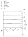
図1に、有機エレクトロルミネッセンス素子の層構成の一例を示す。この有機エレクトロルミネッセンス素子は、基板1と、第1電極2と、発光層5を含む有機層6と、第2電極7とをこの順で備えている。本形態では、有機層6は、第1電極2と発光層5との間に、ホール注入層3及びホール輸送層4をこの順で備えている。有機層6には、発光層5以外に、他の層、例えば、電子輸送層、電子注入層などを適宜、設けてもよい。また、発光層5は、発光層5を構成する発光材料よりも低い屈折率の粒子8を、隣接する層との界面に接触しない状態で、発光層6の内部に有している。すなわち、発光層5に含まれる粒子8は、発光層5の界面に存在しておらず、発光層5と隣接する層(本形態ではホール輸送層4及び第2電極7)に接さない構造となっている。
FIG. 1 shows an example of the layer structure of the organic electroluminescence element. This organic electroluminescence element includes a
基板1としては、基板側片面発光や、両面発光の場合、光を透過させるものであれば特に制限されることなく、適宜の材料の基板1を使用することができる。例えばソーダガラスや無アルカリガラス等のリジッドな透明ガラス板、ポリカーボネートやポリエチレンテレフタレート等のフレキシブルな透明プラスチック板など、任意のものを用いることができるが、これらに限定されるものではない。また、基板反対側片面発光にしてもよい。この場合、基板1としては、上記のようなリジッドな透明ガラス板、透明プラスチック板、フレキシブルな透明プラスチック板に加え、光の透過性は無いが、優れた強度、低コスト、ガスバリア層、耐薬品性、耐熱性等を持つものを用いることができる。さらに、リジッドな金属板、フレキシブルな金属箔など、導電性を示すものは、電極としての機能を果たす可能性があるため、より好ましい。基板1とは反対面から光を取り出す場合も、発光層5の屈折率を下げることで光取り出し量が向上する。
As the
基板1においては、屈折率を、1.5〜1.7程度に設定することができる。また、基板1の厚みを、10〜1000μm程度に設定することができる。
In the
第1電極2及び第2電極7の少なくとも一方は、光を取り出すために光透過性の電極として形成される。第1電極2、第2電極7の材料としては、光透過性を持つ電極の場合、金などの金属、CuI、ITO(インジウム−スズ酸化物)、SnO2、ZnO、IZO(インジウム−亜鉛酸化物)、GZO(ガリウム−亜鉛酸化物)などの金属酸化物などが挙げられる。これらの材料を用い、真空蒸着法や、スパッタリング法などによって電極を形成することができる。ITOやIZOの屈折率は、その組成、成膜方法、結晶構造等により変化するが、ITOはおよそ1.7〜2.3であり、IZOはおよそ1.9〜2.4である。
At least one of the
また、金属ナノ粒子、金属ナノワイヤーを保持する透過性物質をスピンコート、スクリーン印刷、ディップコート、ダイコート、キャスト、スプレーコート、グラビアコートすることでも光透過性の電極を形成することができる。この透過性物質としては、アクリル樹脂、ポリエチレン、ポリプロピレン、ポリエチレンテレフタレート、ポリメチルメタクリレート、ポリスチレン、ポリエーテルスルホン、ポリアリレート、ポリカーボネート樹脂、ポリウレタン、ポリアクリルニトリル、ポリビニルアセタール、ポリアミド、ポリイミド、ジアクリルフタレート樹脂、セルロース系樹脂、ポリ塩化ビニル、ポリ塩化ビニリデン、ポリ酢酸ビニル、その他の熱可塑性樹脂や、これらの樹脂を構成する単量体の2種以上の共重合体が挙げられる。金属ナノ粒子、金属ナノワイヤーなどの導電性を持つ物質としては、銀、金等の金属の微粒子に加え、インジウム−錫酸化物(ITO)、インジウム−亜鉛酸化物(IZO)、錫酸化物等の金属酸化物の微粒子、導電性高分子、導電性の有機材料、ドーパント(ドナーまたはアクセプタ)含有有機材料、導電体と導電性有機材料(高分子含む)の混合物などを挙げることができる。 Alternatively, a light transmissive electrode can be formed by spin coating, screen printing, dip coating, die coating, casting, spray coating, or gravure coating of a transparent material that holds metal nanoparticles and metal nanowires. As this permeable substance, acrylic resin, polyethylene, polypropylene, polyethylene terephthalate, polymethyl methacrylate, polystyrene, polyether sulfone, polyarylate, polycarbonate resin, polyurethane, polyacrylonitrile, polyvinyl acetal, polyamide, polyimide, diacryl phthalate resin , Cellulose resins, polyvinyl chloride, polyvinylidene chloride, polyvinyl acetate, other thermoplastic resins, and copolymers of two or more monomers constituting these resins. Examples of conductive materials such as metal nanoparticles and metal nanowires include indium-tin oxide (ITO), indium-zinc oxide (IZO), and tin oxide in addition to fine metal particles such as silver and gold. Metal oxide fine particles, conductive polymer, conductive organic material, dopant (donor or acceptor) -containing organic material, a mixture of a conductor and a conductive organic material (including polymer), and the like.
第1電極2又は第2電極7が光透過性を有さない電極の場合、電極材料として、Al、Agなどを用いることができるが、これらと他の電極材料を組み合わせて積層構造などとして構成するものであってもよい。このような電極材料の組み合わせとしては、アルカリ金属とAlまたはAgとの積層体、アルカリ金属のハロゲン化物とAlまたはAgとの積層体、アルカリ金属の酸化物とAlまたはAgとの積層体、アルカリ土類金属や希土類金属とAlまたはAgとの積層体、これらの金属種と他の金属との合金などが挙げられ、具体的には、例えばナトリウム、ナトリウム−カリウム合金、リチウム、マグネシウム、バリウムなどとAlとの積層体、カルシウムとAgとの積層体、マグネシウム−銀混合物、マグネシウム−インジウム混合物、アルミニウム−リチウム合金、LiF/Al混合物/積層体、Al/Al2O3混合物などを例として挙げることができる。上記に挙げた材料や形態は一例であり、これらに限定されるものではない。なお、光透過性電極に対向する電極を光反射性の電極として形成した場合、本実施形態では、この反射性電極で反射した光の全反射ロスも低減することが可能である。
In the case where the
第1電極2及び第2電極7の厚みとしては、特に限定されるものではないが、例えば、50〜200nm程度に設定することができる。また、光透過性電極においては、屈折率を、例えば、1.5〜2.4程度に設定することができる。
Although it does not specifically limit as thickness of the
有機層6において、発光層5を形成する発光材料(有機エレクトロルミネッセンス材料)としては、例えば、アントラセン、ナフタレン、ピレン、テトラセン、コロネン、ペリレン、フタロペリレン、ナフタロペリレン、ジフェニルブタジエン、テトラフェニルブタジエン、クマリン、オキサジアゾール、ビスベンゾキサゾリン、ビススチリル、シクロペンタジエン、クマリン、オキサジアゾール、ビスベンゾキサゾリン、ビススチリル、シクロペンタジエン、キノリン金属錯体、トリス(8−ヒドロキシキノリナート)アルミニウム錯体、トリス(4−メチル−8−キノリナート)アルミニウム錯体、トリス(5−フェニル−8−キノリナート)アルミニウム錯体、アミノキノリン金属錯体、ベンゾキノリン金属錯体、トリ−(p−ターフェニル−4−イル)アミン、ピラン、キナクリドン、ルブレン、及びこれらの誘導体、あるいは、1−アリール−2,5−ジ(2−チエニル)ピロール誘導体、ジスチリルベンゼン誘導体、スチリルアリーレン誘導体、スチリルアミン誘導体、ポリフルオレン誘導体、及び、これらの発光性化合物からなる基を分子の一部分に有する化合物あるいは高分子等が挙げられる。また、上記化合物に代表される蛍光色素由来の化合物のみならず、いわゆる燐光発光材料、例えばIr錯体、Os錯体、Pt錯体、ユーロピウム錯体等々の発光材料、又はそれらを分子内に有する化合物若しくは高分子も好適に用いることができる。これらの材料は、必要に応じて、適宜選択して用いることができる。
In the
有機層6における発光層5以外の層、具体的には、ホール注入層3及びホール輸送層4、並びに、電子輸送層、電子注入層は、電子又はホールを注入又は輸送する機能を有する適宜の材料で形成することができる。
Layers other than the light-emitting
有機層6を構成する各層の厚みとしては、特に限定されるものではないが、例えば、発光層5を10〜100nm程度に、ホール注入層3を10〜100nm程度に、ホール輸送層4を10〜100nm程度に、電子注入層を1〜50nm程度に、電子輸送層を10〜100nm程度に、それぞれ設定することができる。また、有機層6を構成する各層の屈折率としては、特に限定されるものではないが、発光層5を1.6〜2.0程度に、ホール注入層3を1.5〜1.8程度に、ホール輸送層4を1.5〜1.8程度に、それぞれ設定することができる。
The thickness of each layer constituting the
ここで、有機エレクトロルミネッセンス素子の発光層5に用いられる発光材料は、ベンゼン環をその分子構造内に多く含んだπ共役結合系の材料が多く、その屈折率は1.6〜2.0程度のものが多い。そのため、発光材料よりも屈折率の低い粒子8は、屈折率が1.6より低い物質を用いることが好ましい。屈折率の下限は特にないが、現実的には大気9よりも高いものであり、例えば、1.1より高いものであってよい。
Here, the light emitting material used for the
粒子8の材料としては、シリカ、炭酸カルシウム、フッ化マグネシウムなどの金属や金属化合物などからなる粒子8が挙げられる。また、アクリル樹脂、ポリエチレン、ポリプロピレン、ポリメチルメタクリレート、ポリスチレン、ポリエーテルスルホン、ポリアリレート、ポリカーボネート樹脂、ポリウレタン、ポリアミド、ポリ塩化ビニル、ポリ塩化ビニリデン、ポリ酢酸ビニル、その他の樹脂や、フッ素を含む低分子化合物などにより構成される粒子8が挙げられるが、これらに限られるものではない。
Examples of the material of the
さらに、上記に示した金属や金属化合物などからなる粒子8のなかでも、粒子内に空隙を含み通常(空隙がない場合)よりも低い屈折率を示す、金属化合物や金属酸化物などからなる多孔質粒子がさらに好ましい。これらの多孔質粒子としてはシリカ多孔質粒子が挙げられる。シリカ多孔質粒子としては、中空シリカ、ナノポーラスシリカ、メソポーラスシリカなどが挙げられる。
Further, among the
多孔質シリカの屈折率は、その空隙率[体積%]より、
(シリカの屈折率)×(1−空隙率/100) + 空隙率/100
で求められる。
From the porosity [volume%] of the refractive index of porous silica,
(Refractive index of silica) × (1−porosity / 100) + porosity / 100
Is required.
この空隙率は高い方が好ましく、例えば、空隙率を20〜40体積%にすることができる。 The porosity is preferably higher. For example, the porosity can be 20 to 40% by volume.
発光層5に混合する発光材料よりも屈折率の低い粒子8は、一般的な有機エレクトロルミネッセンス素子の発光層5が数十nm〜数百nmであるため、その大きさ(粒径)は10〜100nmが好ましい。なお、粒子8の粒径は、レーザー回折粒度分布計などを用いたレーザー回折散乱法や、電子顕微鏡などにより測定することができる。
The
メソポーラスシリカは、例えば、メソ孔に界面活性剤を有する界面活性剤複合シリカ微粒子を調製し、この界面活性剤複合シリカ微粒子から界面活性剤を抽出して除去することにより製造することができる。具体的には、例えば、まず、水、NH3水溶液、エチレングリコール、ヘキサデシルトリメチルアンモニウムブロマイド(CTAB)、1,3,5−トリメチルベンゼン(TMB)、テトラエトキシシラン、γ−アミノプロピルトリエトキシシランを混合し撹拌して界面活性剤複合シリカ微粒子を作製する。次に、イソプロパノール、5N−HCl、ヘキサメチルジシロキサンを混合して攪拌しておき、これに界面活性剤複合シリカ微粒子の合成反応液を添加し、攪拌・還流する。以上の操作により、界面活性剤複合シリカ微粒子から界面活性剤及び疎水部含有添加物が抽出され、粒子表面がトリメチルシリル化されたメソポーラスシリカ微粒子が得られる。そして、トリメチルシリル化後の溶液を遠心分離後、液を除去し、沈殿した固相にエタノールを加え、振とう機で粒子をエタノール中で振とうすることでメソポーラスシリカ微粒子が洗浄される。さらに、作製したメソポーラスシリカ微粒子にイソプロパノールを加えて、振とう機で再分散させることにより、イソプロパノールに分散したメソポーラスシリカ微粒子が得られる。以上の例は、メソポーラスシリカの製法の一例であり、この製法に限定されるものではない。 Mesoporous silica can be produced, for example, by preparing surfactant composite silica fine particles having a surfactant in mesopores and extracting and removing the surfactant from the surfactant composite silica fine particles. Specifically, for example, first, water, NH 3 aqueous solution, ethylene glycol, hexadecyltrimethylammonium bromide (CTAB), 1,3,5-trimethylbenzene (TMB), tetraethoxysilane, γ-aminopropyltriethoxysilane Are mixed and stirred to produce surfactant composite silica fine particles. Next, isopropanol, 5N HCl, and hexamethyldisiloxane are mixed and stirred, and a synthetic reaction liquid of surfactant composite silica fine particles is added thereto, followed by stirring and refluxing. By the above operation, the surfactant and the hydrophobic part-containing additive are extracted from the surfactant composite silica fine particles, and mesoporous silica fine particles whose surface is trimethylsilylated are obtained. Then, the solution after trimethylsilylation is centrifuged, the liquid is removed, ethanol is added to the precipitated solid phase, and the particles are shaken in ethanol with a shaker to wash the mesoporous silica fine particles. Furthermore, by adding isopropanol to the prepared mesoporous silica fine particles and redispersing with a shaker, mesoporous silica fine particles dispersed in isopropanol can be obtained. The above example is an example of a method for producing mesoporous silica, and is not limited to this method.
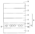
発光層5に含まれる粒子8が、発光層5と隣接する層との界面に接触しないようにするには、図2に示すように、発光層5が複数の領域が積層されて形成されていることが好ましい。具体的には、次のようにして発光層5を形成することができる。まず、基板1の表面に光透過性のある第1電極2、ホール注入層3、ホール輸送層4を順に成膜した積層体を形成する。次に、この積層体のホール輸送層4の表面に対して、発光材料のみを成膜し、発光層5の第1領域51を形成する。そして、発光層5の第1領域51の表面に、発光材料よりも屈折率の低い粒子8のみを積層する。この粒子8の積層は、粒子分散液の塗布や、粒子の吹き付けなどにより行うことができる。そしてさらに、粒子8が積層された表面に、発光材料のみを成膜し、発光層5の第2領域52を形成する。このとき、粒子8は第1領域51に付着したり、粒子8同士で付着したりしているので、第2領域52によって埋め込まれることとなる。そして、第2領域52は、第1領域51との界面に粒子8が存在する領域として形成される。そして、必要に応じ有機層の他の層を積層した後、第2電極7をその上に成膜することで、図2に示すような有機エレクトロルミネッセンス素子が得られる。この有機エレクトロルミネッセンスでは、複数の粒子8が発光層5の内部において略同一平面上に配置されている。また、第1領域51と第2領域52とは同じ発光材料が用いられることによって、積層後は一体化した発光層5を形成する。なお、発光層5の作製方法は、この方法に限定されるものではない。例えば、上記のように作製した発光層5の第1領域51(発光材料領域)の上に、粒子8と発光材料とを混合した混合領域を成膜して形成し、さらにその上に発光材料のみを成膜して発光材料領域を形成するようにしてもよい。
In order to prevent the
発光層5内における粒子8の量としては、特に限定されるものではないが、屈折率の低下と発光性の確保の観点から、例えば、発光層5全体に対しての体積率が、20〜40体積%であることが好ましい。
The amount of the
上記の有機エレクトロルミネッセンス素子では、発光層5が発光材料よりも低い屈折率の粒子を含むことで、発光層5の屈折率が低減される。また、発光層5に存在する屈折率の低い粒子8は、発光源10から斜めに高角度に出射した光など、発光源10からの光を全反射しにくいものとすることができる(図3参照)。これは、第1電極2と基板1の界面、及び、基板1と大気9の界面での臨界角を大きくすることができるためであると推測される。また、光の角度を発光層5で変化させて全反射しにくい角度で発光層5から基板1に向かって光を出射するためであると推測される。このように、本実施形態の有機エレクトロルミネッセンス素子は、発光層5に粒子8が含まれていることにより、発光層5が発光材料のみからなる場合と比較して、第1電極2から基板1への光取出し量、及び、基板1から大気9への光取出し量を増加させることができるので、光取り出し効率を向上することができるものである。また、低屈折率の粒子8が発光層5と隣接する層との界面に存在しないことで、ダークスポットの発生を抑制することができるものである。
In said organic electroluminescent element, the refractive index of the
(実施例1)
(低屈折率粒子の調製)
冷却管、攪拌機、温度計を取り付けたセパラブルフラスコに、H2O:120g、25%NH3水溶液:5.4g、エチレングリコール:20g、ヘキサデシルトリメチルアンモニウムブロマイド(CTAB):1.2g、1,3,5−トリメチルベンゼン(TMB):1.58g(物質量比TMB/CTAB=4)、TEOS:1.29g、γ−アミノプロピルトリエトキシシラン:0.23gを混合し、60℃で4時間攪拌することで、界面活性剤複合シリカ微粒子を作製した。
Example 1
(Preparation of low refractive index particles)
In a separable flask equipped with a condenser, a stirrer, and a thermometer, H 2 O: 120 g, 25% NH 3 aqueous solution: 5.4 g, ethylene glycol: 20 g, hexadecyltrimethylammonium bromide (CTAB): 1.2 g, 1 , 3,5-trimethylbenzene (TMB): 1.58 g (substance quantity ratio TMB / CTAB = 4), TEOS: 1.29 g, γ-aminopropyltriethoxysilane: 0.23 g are mixed, and 4 at 60 ° C. Surfactant composite silica fine particles were prepared by stirring for a period of time.
次に、イソプロパノール:30g、5N−HCl:60g、ヘキサメチルジシロキサン:26gを混合し、72℃で攪拌しておき、界面活性剤複合シリカ微粒子の合成反応液を添加し、30分間攪拌・還流した。以上の操作により、界面活性剤複合シリカ微粒子から界面活性剤及び疎水部含有添加物が抽出され、粒子表面がトリメチルシリル化されたメソポーラスシリカ微粒子を得た。 Next, isopropanol: 30 g, 5N-HCl: 60 g, hexamethyldisiloxane: 26 g are mixed and stirred at 72 ° C., a synthetic reaction solution of surfactant composite silica fine particles is added, and the mixture is stirred and refluxed for 30 minutes. did. Through the above operation, the surfactant and the hydrophobic part-containing additive were extracted from the surfactant composite silica fine particles to obtain mesoporous silica fine particles whose surface was trimethylsilylated.
トリメチルシリル化後の溶液を20,000rpm,20分間で遠心分離後、液を除去した。沈殿した固相にエタノールを加え、振とう機で粒子をエタノール中で振とうすることでメソポーラスシリカ微粒子を洗浄した。20,000rpm,20分間で遠心分離し、液を除去しメソポーラスシリカ微粒子を得た。 The solution after trimethylsilylation was centrifuged at 20,000 rpm for 20 minutes, and then the liquid was removed. Ethanol was added to the precipitated solid phase, and the mesoporous silica fine particles were washed by shaking the particles in ethanol with a shaker. Centrifugation was performed at 20,000 rpm for 20 minutes, and the liquid was removed to obtain mesoporous silica fine particles.
作製したメソポーラスシリカ微粒子0.2gにイソプロパノール3.8gを加えて、振とう機で再分散させたところ、イソプロパノールに分散したメソポーラスシリカ微粒子を得た。メソポーラスシリカ微粒子の粒子径は、約50nmであった。また、同様の方法にて、メソポーラスシリカ微粒子を1−ブタノールに再分散させた溶液を調製した。メソポーラスシリカ微粒子の屈折率(波長650nm)は、1.3であった。 When 3.8 g of isopropanol was added to 0.2 g of the prepared mesoporous silica fine particles and redispersed with a shaker, mesoporous silica fine particles dispersed in isopropanol were obtained. The particle diameter of the mesoporous silica fine particles was about 50 nm. Further, a solution in which mesoporous silica fine particles were redispersed in 1-butanol was prepared by the same method. The refractive index (wavelength 650 nm) of the mesoporous silica fine particles was 1.3.
(素子の作製)
基板1として無アルカリガラス板(コーニング社製「No.1737」、屈折率1.50〜1.53(波長500nm)、厚み0.7μm)を用いた。この基板1上に、ITO(スズドープ酸化インジウム)ターゲット(東ソー製)を用いてスパッタを行い、膜厚150nmのITO層を形成した。得られたITO層付ガラス基板を、Ar雰囲気下200℃で1時間アニール処理を行い、シート抵抗18Ω/□の第1電極2を形成した。第1電極2の波長650nmでの屈折率をSCI社製FilmTekで測定したところ2.05であった。
(Production of element)
An alkali-free glass plate (Corning “No. 1737”, refractive index of 1.50 to 1.53 (wavelength 500 nm), thickness of 0.7 μm) was used as the
次に、第1電極2上にポリエチレンジオキシチオフェン/ポリスチレンスルホン酸(PEDOT−PSS)(H.C.Starck社製「CLEVIOS P AI4083」、PEDOT:PSS=1:6)を膜厚30nmになるようにスピンコーターで塗布し、150℃で10分間焼成することにより、ホール注入層3を作製した。ホール注入層3の波長650nmでの屈折率をSCI社製FilmTekで測定したところ1.55であった。
Next, polyethylenedioxythiophene / polystyrene sulfonic acid (PEDOT-PSS) (“CLEVIOS PAI4083” manufactured by HC Starck, PEDOT: PSS = 1: 6) is formed to a thickness of 30 nm on the
次に、TFB(Poly[(9,9-dioc tylfluorenyl-2,7-diyl)-co-(4,4’-(N-(4-sec-butylphenyl))diphenylamine)])(アメリカンダイソース社製「HoleTransport Polymer ADS259BE」)をTHF溶媒に溶解した溶液を、ホール注入層3の上に膜厚12nmになるようにスピンコーターで塗布してTFB被膜を作製し、これを200℃で10分間焼成することによって、ホール輸送層4を作製した。ホール輸送層4の波長650nmでの屈折率をSCI社製FilmTekで測定したところ1.7であった。
Next, TFB (Poly [(9,9-dioc tylfluorenyl-2,7-diyl) -co- (4,4 ′-(N- (4-sec-butylphenyl)) diphenylamine)]) (American Dye Source) "HoleTransport Polymer ADS259BE") in THF solvent was applied to the
次に、赤色高分子(アメリカンダイソース社製「LightEmittingpolymer ADS111RE」、波長650nmでの屈折率約1.7)をTHF溶媒に溶解した溶液を、ホール輸送層4の上に膜厚が20nmになるようにスピンコーターで塗布し、100℃で10分間焼成することによって、発光層5のうちの、発光材料のみを含む第1領域51を作製した。この第1領域51の上に、上記で調製したメソポーラスシリカを1−ブタノールに分散させた溶液を塗布した。さらにその上に、赤色高分子(アメリカンダイソース社製「Light Emitting polymer ADS111RE」)をTHF溶媒に溶解した溶液を、スピンコーターで塗布し、100℃で10分間焼成することによって、発光層5のうち、発光材料よりも低い屈折率を持つ粒子を、第1領域51との界面に有する第2領域52を作製した。このとき、発光層5の全体の膜厚が100nmになるように成膜した。発光層5の波長650nmでの屈折率をSCI社製FilmTekで測定したところ1.60であった。
Next, a solution in which a red polymer ("LightEmittingpolymer ADS111RE" manufactured by American Dye Source Co., Ltd., refractive index of about 1.7 at a wavelength of 650 nm) is dissolved in a THF solvent is formed on the
発光層5の上に電子注入層として、Ba(高純度化学製)を5nmの膜厚で真空蒸着により形成した。そして、電子注入層の上にAl(高純度化学社製)を80nmの膜厚で真空蒸着し、陰極として第2電極7を形成した。これにより有機エレクトロルミネッセンス素子が得られた。
Ba (manufactured by High-Purity Chemical) was formed as an electron injection layer on the light-emitting
この後、上記の各層を形成した基板1を露点−80℃以下のドライ窒素雰囲気のグローブボックスに大気に暴露することなく搬送した。一方、硝子製の封止キャップに吸水剤(ダイニック社製)を貼り付けると共に封止キャップの外周部に紫外線硬化樹脂製のシール剤を塗布したものを予め用意した。そしてグローブボックス内で各層を囲むように封止キャップを基板1にシール剤で張り合わせ、紫外線照射してシール剤を硬化させることによって、各層を封止キャップで封止し、封止された有機エレクトロルミネッセンス素子を得た。
Then, the board |
(比較例1)
発光層5について、赤色高分子(アメリカンダイソース社製「Light Emitting polymer ADS111RE」)をTHF溶媒に溶解した溶液を、ホール輸送層4の上に膜厚が100nmになるようにスピンコーターで塗布し、100℃で10分間焼成することによって、発光層5を成膜した。それ以外は、実施例1と同様にして、有機エレクトロルミネッセンス素子を作製した。発光層5の波長650nmでの屈折率をSCI社製FilmTekで測定したところ1.70であった。
(Comparative Example 1)
For the
(比較例2)
発光層5について、赤色高分子(アメリカンダイソース社製「Light Emitting polymer ADS111RE」)と、実施例1にて調製したメソポーラスシリカとをTHF溶媒に混合した溶液(発光材料:メソポーラスシリカは体積比で4:1)を、ホール輸送層4の上に膜厚が100nmになるようにスピンコーターで塗布し、100℃で10分間焼成することによって、発光層5を成膜した。それ以外は、実施例1と同様にして、有機エレクトロルミネッセンス素子を得た。発光層5の波長650nmでの屈折率をSCI社製FilmTekで測定したところ1.60であった。
(Comparative Example 2)
For the light-emitting
(評価)
実施例、比較例で得られた有機エレクトロルミネッセンス素子の特性の評価を表1に示す。
(Evaluation)
Table 1 shows the evaluation of the characteristics of the organic electroluminescence elements obtained in Examples and Comparative Examples.
表1にみられるように、発光層5に低屈折率の粒子8を含み、発光層5の屈折率を低減させた実施例1の素子は、粒子8を含まない通常の屈折率の発光層5を有する比較例1に比べて、光取出し効率が向上している。また、低屈折率の粒子8が、ホール輸送層4、及び、電子注入層と接している比較例2では、ダークスポットが発生し、光取り出し性を評価することができなかった。
As can be seen from Table 1, the

1 基板
2 第1電極
3 ホール注入層
4 ホール輸送層
5 発光層
6 有機層
7 第2電極
8 粒子
9 大気
51 第1領域
52 第2領域
DESCRIPTION OF
Claims (2)
Priority Applications (1)
| Application Number | Priority Date | Filing Date | Title |
|---|---|---|---|
| JP2011119538A JP2012248696A (en) | 2011-05-27 | 2011-05-27 | Organic electroluminescent element |
Applications Claiming Priority (1)
| Application Number | Priority Date | Filing Date | Title |
|---|---|---|---|
| JP2011119538A JP2012248696A (en) | 2011-05-27 | 2011-05-27 | Organic electroluminescent element |
Publications (1)
| Publication Number | Publication Date |
|---|---|
| JP2012248696A true JP2012248696A (en) | 2012-12-13 |
Family
ID=47468882
Family Applications (1)
| Application Number | Title | Priority Date | Filing Date |
|---|---|---|---|
| JP2011119538A Withdrawn JP2012248696A (en) | 2011-05-27 | 2011-05-27 | Organic electroluminescent element |
Country Status (1)
| Country | Link |
|---|---|
| JP (1) | JP2012248696A (en) |
-
2011
- 2011-05-27 JP JP2011119538A patent/JP2012248696A/en not_active Withdrawn
Similar Documents
| Publication | Publication Date | Title |
|---|---|---|
| JP5658913B2 (en) | Organic electroluminescence device | |
| JP5821038B2 (en) | Organic electroluminescence device | |
| KR101160736B1 (en) | Surface light emitting body | |
| JP6220870B2 (en) | ORGANIC LIGHT EMITTING DIODE (OLED) ELEMENT LAMINATE, ITS MANUFACTURING METHOD, AND ORGANIC LIGHT EMITTING DIODE (OLED) ELEMENT HAVING THE SAME | |
| JP6345244B2 (en) | Organic electronic equipment | |
| JP5824678B2 (en) | Organic electroluminescence device | |
| WO2011162080A1 (en) | Organic electroluminescence element | |
| JP6573160B2 (en) | Light emitting element | |
| CN103460430B (en) | Organic EL element and its manufacturing method | |
| TWI506836B (en) | Transparent conductive film and organic light-emitting device therewith | |
| CN104106310B (en) | Organic electroluminescent device | |
| JP2012009225A (en) | Organic electroluminescent element and method of manufacturing the same | |
| JP2012009336A (en) | Organic electroluminescent element | |
| JP2013089501A (en) | Organic electroluminescent element | |
| JP2012248696A (en) | Organic electroluminescent element | |
| JP2013097966A (en) | Organic electroluminescence element | |
| JP2013030585A (en) | Organic electroluminescent element | |
| JP2012119524A (en) | Organic electroluminescent element | |
| JP2011048999A (en) | Organic electroluminescent element | |
| KR101947008B1 (en) | Electrode and organic light emitting device comprising the same | |
| JP2013008624A (en) | Organic electroluminescent element | |
| WO2012161057A1 (en) | Organic electroluminescence element | |
| WO2012161113A1 (en) | Organic electroluminescence element | |
| WO2012176584A1 (en) | Organic electroluminescent element | |
| WO2012165159A1 (en) | Organic electroluminescent element and method for manufacturing same |
Legal Events
| Date | Code | Title | Description |
|---|---|---|---|
| A300 | Application deemed to be withdrawn because no request for examination was validly filed |
Free format text: JAPANESE INTERMEDIATE CODE: A300 Effective date: 20140805 |