JP2012247474A - Electrophotographic photoreceptor - Google Patents
Electrophotographic photoreceptor Download PDFInfo
- Publication number
- JP2012247474A JP2012247474A JP2011116676A JP2011116676A JP2012247474A JP 2012247474 A JP2012247474 A JP 2012247474A JP 2011116676 A JP2011116676 A JP 2011116676A JP 2011116676 A JP2011116676 A JP 2011116676A JP 2012247474 A JP2012247474 A JP 2012247474A
- Authority
- JP
- Japan
- Prior art keywords
- protective layer
- layer
- fine particles
- metal oxide
- oxide fine
- Prior art date
- Legal status (The legal status is an assumption and is not a legal conclusion. Google has not performed a legal analysis and makes no representation as to the accuracy of the status listed.)
- Granted
Links
Images

Landscapes
- Photoreceptors In Electrophotography (AREA)
Abstract
Description
本発明は、電子写真感光体に関し、更に詳しくは電子写真方式を利用した画像形成装置に用いられる電子者写真感光体に関する。 The present invention relates to an electrophotographic photoreceptor, and more particularly to an electrophotographic photoreceptor used in an image forming apparatus using an electrophotographic system.
近年、電子写真感光体は有機光導電性物質を含有する有機感光体が広く用いられている。有機感光体は可視光から赤外光まで各種露光光源に対応した材料を開発しやすいこと、環境汚染のない材料を選択できること、製造コストが安いことなどが無機系の感光体に対して有利な点である。 In recent years, organic photoreceptors containing organic photoconductive materials have been widely used as electrophotographic photoreceptors. Organic photoconductors are advantageous for inorganic photoconductors because it is easy to develop materials compatible with various exposure light sources from visible light to infrared light, the ability to select materials without environmental pollution, and low manufacturing costs. Is a point.
一方、電子写真感光体(以下感光体とも言う)は帯電、露光、現像、転写、クリーニング等により、電気的あるいは機械的な外力を直接受けているため、画像形成が繰り返し行われても帯電安定性、電位保持性など安定して維持する耐久性が求められている。 On the other hand, an electrophotographic photosensitive member (hereinafter also referred to as a photosensitive member) is directly charged with electrical or mechanical external force by charging, exposure, development, transfer, cleaning, etc., so that charging is stable even when image formation is repeated. The durability which maintains stably, such as a property and electric potential retention property is calculated | required.
特に近年デジタル化の流れの中で、高精細、高画質の画像への要求が高まり、溶解懸濁トナーや乳化重合凝集トナーなどの重合法による小粒径のトナーが主流になっており、これらの小粒径のトナーは感光体表面への付着力が大きく、感光体表面に付着した転写残トナーなどの残留トナーの除去が不十分となりやすい。ゴムブレードを用いたクリーニング方式では、トナーがブレードを通過する「トナーすり抜け」やブレードが反転する「ブレード捲れ」、あるいは感光体とブレードの擦過音の発生、いわゆる「ブレード鳴き」と言った現象が発生しやすい。上記「トナーすり抜け」を解決するためにはブレードの感光体への当接圧力を高くする必要があるが、繰り返し使用することにより、有機感光体の表面が摩耗し耐久性が不足するという問題が発生する。また帯電時に発生するオゾンや窒素酸化物による劣化に対しても十分な耐久性を有することが求められている。 In recent years, especially in the digital trend, demand for high-definition and high-quality images has increased, and toners with small particle diameters by polymerization methods such as dissolved suspension toners and emulsion polymerization aggregation toners have become mainstream. The toner having a small particle size has a large adhesion force to the surface of the photoconductor, and the removal of residual toner such as transfer residual toner adhering to the surface of the photoconductor tends to be insufficient. In the cleaning method using a rubber blade, there are phenomena such as "toner slipping" where the toner passes through the blade, "blade curl" where the blade is reversed, or the generation of scratching noise between the photoconductor and the blade, so-called "blade squealing" Likely to happen. In order to solve the above “toner slipping”, it is necessary to increase the contact pressure of the blade to the photosensitive member. However, the repeated use causes a problem that the surface of the organic photosensitive member is worn and the durability is insufficient. appear. Further, it is required to have sufficient durability against deterioration caused by ozone and nitrogen oxides generated during charging.
このような経緯から感光体表面に保護層(以下表面層ともいう)を設けて機械的強度を向上させる技術が提案されている。 For these reasons, a technique has been proposed in which a protective layer (hereinafter also referred to as a surface layer) is provided on the surface of the photoreceptor to improve the mechanical strength.
具体的には、感光体保護層に一般に硬化性化合物と呼ばれる重合性化合物を使用し、塗布した後硬化反応を行うことで、クリーニングブレード等の摩擦による表面の摩耗や傷の発生に対して耐久性の高い感光体を作製する技術が提案されている(例えば特許文献1、特許文献2参照)。
Specifically, a polymerizable compound generally called a curable compound is used for the photoconductor protective layer, and after the coating, a curing reaction is performed, thereby being resistant to surface abrasion and scratches caused by friction of a cleaning blade or the like. A technique for producing a highly sensitive photoreceptor has been proposed (see, for example,
更にシリカなどの無機微粒子を保護層に分散させ、機械的強度を向上させる技術が提案されている(例えば特許文献3、特許文献4参照)。 Further, a technique for improving the mechanical strength by dispersing inorganic fine particles such as silica in a protective layer has been proposed (see, for example, Patent Document 3 and Patent Document 4).
近年、電子写真方式の画像形成装置は、軽印刷分野への利用が急拡大しており、電子写真感光体には更なる高耐久化、高画質化が要請されている。しかし、これら従来技術では耐久性、画質において十分満足出来る電子写真感光体を得ることが出来ず、電子写真感光体にはなお一層の高耐久、高画質化技術が望まれていた。 In recent years, the use of electrophotographic image forming apparatuses in the light printing field has been rapidly expanding, and electrophotographic photoreceptors are required to have higher durability and higher image quality. However, these conventional techniques cannot provide an electrophotographic photosensitive member that is sufficiently satisfactory in terms of durability and image quality, and further high durability and high image quality technologies have been desired for the electrophotographic photosensitive member.
電子写真感光体(以下簡単に感光体ともいう)の耐久性を向上するために、感光層表面に耐摩耗性の高い保護層を設けることが有効である。この保護層として、ラジカル重合性化合物と、アクリロイル基、メタクリロイル基などの反応性の有機基を有する表面処理剤で処理した金属酸化物微粒子との反応生成物を含有する硬化型の保護層を感光層の上に設けることが有効である。 In order to improve the durability of an electrophotographic photosensitive member (hereinafter also referred to simply as a photosensitive member), it is effective to provide a protective layer with high wear resistance on the surface of the photosensitive layer. As this protective layer, a curable protective layer containing a reaction product of a radical polymerizable compound and metal oxide fine particles treated with a surface treatment agent having a reactive organic group such as an acryloyl group or a methacryloyl group is photosensitive. It is effective to provide it on the layer.
しかし、保護層の硬度が高すぎると保護層の剛直性が増大して脆くなり、保護層の減耗が進行しやすくなってしまう。この剛直性は、保護層の形成に用いる溶媒の保護層中における含有量にも相関し、含有溶媒量が少ないと、剛直性が高くなり摩耗が進行しやすくなる。また、含有溶媒量が多いと、剛直性は低下するが、電子写真の画像形成プロセスにおいて、露光によって生じた正孔(ホール)が保護層中に含有される溶媒にトラップされやすく、電荷移動がスムースに行われないため画像のムラが発生する。特に印刷された同濃度の画像の中で感光体周期による濃度差が発生してしまうという問題が生じる。このように耐摩耗性向上と画像安定性の両立は極めて困難であった。 However, if the hardness of the protective layer is too high, the rigidity of the protective layer increases and becomes brittle, and the wear of the protective layer tends to progress. This rigidity correlates with the content of the solvent used for forming the protective layer in the protective layer. When the amount of the solvent is small, the rigidity becomes high and the wear tends to proceed. In addition, when the content of the solvent is large, the rigidity decreases, but in the electrophotographic image forming process, holes generated by exposure are easily trapped in the solvent contained in the protective layer, and charge transfer is caused. Since it is not performed smoothly, image unevenness occurs. In particular, there arises a problem that a density difference due to the photoconductor cycle occurs in the printed image having the same density. Thus, it has been extremely difficult to achieve both improved wear resistance and image stability.
本発明は上記課題を解決するために成されたもので、耐摩耗性に優れ、感光体周期による濃度差が発生せず、耐摩耗性と画像特性の安定性が両立する電子写真感光体を提供することを目的としている。 The present invention has been made in order to solve the above-mentioned problems. An electrophotographic photoreceptor excellent in abrasion resistance, causing no difference in density due to the photoreceptor cycle, and having both abrasion resistance and stability of image characteristics is provided. It is intended to provide.
本発明の上記課題は以下の構成とすることによって解決される。
1.導電性支持体上に少なくとも感光層と保護層とを順次積層して成る電子写真感光体において、該保護層がラジカル重合性化合物の反応物と金属酸化物微粒子を含有しており、該保護層の塗布に用いられる溶媒がアルコール類とケトン類から選ばれる少なくとも1種であって、該保護層に含有される溶媒量の合計が、20ppm以上75ppm以下であることを特徴とする電子写真感光体。
2.前記保護層の塗布に用いられる溶媒がアルコール類1種及びケトン類1種からなる混合溶媒であることを特徴とする前記1に記載の電子写真感光体。
3.前記金属酸化物微粒子が、アルミナ微粒子、酸化スズ微粒子、酸化チタン微粒子から選択される少なくとも何れか1種であることを特徴とする前記1または前記2に記載の電子写真感光体。
4.前記金属酸化物微粒子が表面処理剤で処理したものであって、該表面処理剤が、アクリロイル基、メタクリロイル基の少なくとも何れかを含有する化合物であることを特徴とする前記1から前記3の何れか1項に記載の電子写真感光体。
5.前記ラジカル重合性化合物が、構造中にアクリロイル基、またはメタクリロイル基の少なくとも何れかを有する重合性単量体、または重合性オリゴマーであることを特徴とする前記1から前記4の何れか1項に記載の電子写真感光体。
The above-described problems of the present invention are solved by the following configuration.
1. An electrophotographic photosensitive member in which at least a photosensitive layer and a protective layer are sequentially laminated on a conductive support, wherein the protective layer contains a reaction product of a radical polymerizable compound and metal oxide fine particles, and the protective layer The electrophotographic photoreceptor, wherein the solvent used for coating is at least one selected from alcohols and ketones, and the total amount of solvents contained in the protective layer is 20 ppm to 75 ppm .
2. 2. The electrophotographic photoreceptor according to 1 above, wherein the solvent used for coating the protective layer is a mixed solvent composed of one kind of alcohol and one kind of ketone.
3. 3. The electrophotographic photoreceptor according to 1 or 2 above, wherein the metal oxide fine particles are at least one selected from alumina fine particles, tin oxide fine particles, and titanium oxide fine particles.
4). The metal oxide fine particles are treated with a surface treatment agent, and the surface treatment agent is a compound containing at least one of an acryloyl group and a methacryloyl group. 2. The electrophotographic photosensitive member according to
5. Any one of 1 to 4 above, wherein the radical polymerizable compound is a polymerizable monomer having at least one of an acryloyl group and a methacryloyl group in the structure, or a polymerizable oligomer. The electrophotographic photosensitive member described.
本発明は上記の構成を採ることによって、耐摩耗性が高く画像安定性の優れた高耐久感光体を提供することが出来る。 By adopting the above configuration, the present invention can provide a highly durable photoreceptor having high wear resistance and excellent image stability.
以下本発明を実施するための形態について詳細に説明するが、本発明はこれらに限定されるものではない。 DESCRIPTION OF EMBODIMENTS Hereinafter, embodiments for carrying out the present invention will be described in detail, but the present invention is not limited thereto.
本発明の感光体は耐摩耗性の向上を目的に、導電性支持体上に少なくとも感光層と保護層を順次積層した構成のものである。この保護層は、少なくともラジカル重合性化合物の反応生成物と金属酸化物微粒子を含有する。金属酸化物微粒子は、アクリロイル基、メタクリロイル基を有するラジカル重合性表面処理剤で表面処理されていることが好ましく、これにより、ラジカル重合性化合物と金属酸化物微粒子の表面処理剤が架橋反応を行い、保護層の硬度を更に上げることが出来る。この保護層は塗布によって形成され、塗布に用いる溶媒としてはアルコール類及びケトン類から選択される。保護層は塗布した後、乾燥し、その後、熱、あるいは光により硬化処理を行う。この時、保護層の塗布に用いたアルコール及びケトン類の合計の溶媒量が、保護層中20ppm以上75ppm以下であると感光体の耐摩耗性と画像特性の両方を満足することを見出したものである。 The photoreceptor of the present invention has a structure in which at least a photosensitive layer and a protective layer are sequentially laminated on a conductive support for the purpose of improving wear resistance. This protective layer contains at least a reaction product of a radical polymerizable compound and metal oxide fine particles. The metal oxide fine particles are preferably surface-treated with a radical polymerizable surface treatment agent having an acryloyl group or a methacryloyl group, whereby the radical polymerizable compound and the surface treatment agent of the metal oxide fine particles undergo a crosslinking reaction. The hardness of the protective layer can be further increased. This protective layer is formed by coating, and the solvent used for coating is selected from alcohols and ketones. After the protective layer is applied, it is dried and then cured by heat or light. At this time, it was found that when the total amount of alcohol and ketone used for coating the protective layer is 20 ppm or more and 75 ppm or less in the protective layer, both the wear resistance and image characteristics of the photoreceptor are satisfied. It is.
保護層中に含有される溶媒量(以下含有溶媒量とも言う)が上記範囲であると耐摩耗性と画像特性の両方が良好になる理由は以下の理由によるものと考えられる。 The reason why both the wear resistance and the image characteristics are improved when the amount of the solvent contained in the protective layer (hereinafter also referred to as the amount of solvent contained) is in the above range is considered to be as follows.
即ち、保護層中の含有溶媒量が少ないと保護層の剛直性が高くなり、保護層が脆くなってしまう。このため繰り返し使用に伴う摩擦により、保護層の減耗が進み、耐久性が低下してしまう。含有溶媒量が多いと保護層はある程度柔軟性を保つため耐摩耗性が向上する。しかし、一方、含有溶媒が正孔(ホール)のトラップとして働くため、含有溶媒量が多いと電位特性の変化が大きくなり、それが感光体の周期により、画像濃度の変動となって顕在化する。即ち、同じ濃度の画像を印刷した時に感光体の周期に従って、画像濃度の差として現われるものと考えられる。即ち、感光体の一周目と二周目で画像濃度差が現われてしまう。 That is, if the amount of the solvent contained in the protective layer is small, the rigidity of the protective layer increases and the protective layer becomes brittle. For this reason, the wear of the protective layer proceeds due to friction caused by repeated use, and durability is lowered. When the content of the solvent is large, the protective layer is kept flexible to some extent, so that the wear resistance is improved. However, since the contained solvent acts as a hole trap, if the amount of the contained solvent is large, the change in potential characteristics becomes large, and this is manifested as a change in image density due to the period of the photoconductor. . That is, it is considered that when an image having the same density is printed, it appears as a difference in image density according to the period of the photosensitive member. That is, a difference in image density appears between the first and second rounds of the photoreceptor.
本発明においては、保護層中の含有溶媒量を上記範囲に管理することで、感光体の周期によって現われる画像濃度差と保護層の耐摩耗性とを両立させることが出来ることを見出し、画像特性と耐摩耗性とに優れた高耐久感光体を得ることが出来たものである。 In the present invention, by controlling the amount of solvent contained in the protective layer within the above range, it has been found that both the image density difference that appears depending on the period of the photoreceptor and the wear resistance of the protective layer can be achieved. And a highly durable photoconductor excellent in wear resistance.
≪溶媒量≫
本発明においては、感光体の保護層は、アルコール類およびケトン類から選択される少なくとも1種の溶媒によって塗布形成される。また、保護層の塗布に用いられる溶媒は、アルコール類1種とケトン類1種の混合溶媒が好ましい。これらのアルコール、ケトンなどの溶媒量が保護層中20ppm以上75ppm以下である。保護層中の溶媒量が40ppm以上60ppm以下であるとさらに好ましい。溶媒量がこの範囲であると感光体の耐摩耗性と画像特性が安定する。即ち、20ppm以下では保護層の剛直性が高くなりすぎ耐摩耗性が劣ってしまう。また75ppm以上では、トラップされる正孔が増え、電位特性の変化量が多くなり、その結果、感光体周期の画像濃度差が大きくなる。
≪Solvent amount≫
In the present invention, the protective layer of the photoreceptor is formed by coating with at least one solvent selected from alcohols and ketones. Moreover, the solvent used for coating of the protective layer is preferably a mixed solvent of one kind of alcohol and one kind of ketone. The amount of these alcohols, ketones and other solvents is 20 ppm to 75 ppm in the protective layer. More preferably, the amount of solvent in the protective layer is 40 ppm or more and 60 ppm or less. When the amount of the solvent is within this range, the wear resistance and image characteristics of the photoreceptor are stabilized. That is, at 20 ppm or less, the rigidity of the protective layer becomes too high and the wear resistance is poor. On the other hand, when the concentration is 75 ppm or more, the number of trapped holes increases and the amount of change in potential characteristics increases, and as a result, the image density difference in the photoreceptor period increases.
(溶媒量の測定法)
保護層中に含有される溶媒量は、電荷輸送層と保護層とをガスクロマトグラフ質量分析計で分析することによって測定することが出来る。本発明における保護層中の溶媒量は以下のようにして測定した値である。
(Measurement method of solvent amount)
The amount of solvent contained in the protective layer can be measured by analyzing the charge transport layer and the protective layer with a gas chromatograph mass spectrometer. The amount of solvent in the protective layer in the present invention is a value measured as follows.
(試料)
感光体の電荷輸送層及び表面層をカッターナイフ等により剥離し、剥離した膜0.1gを容積20mlのサンプル瓶に入れ、130℃、30分の加熱を行い、ヘッドスペース(HS)法にて測定する。
(sample)
The charge transport layer and the surface layer of the photoreceptor are peeled off with a cutter knife or the like, 0.1 g of the peeled film is put into a sample bottle having a volume of 20 ml, heated at 130 ° C. for 30 minutes, and headspace (HS) method. taking measurement.
(HS−GC/MS測定条件)
測定器:ガスクロマトグラフ分析計GC/HP6890及びMS/HP5973(アジレント・テクノロジー社製)
GCカラム:DB−624(内径:0.25mm、長さ:30m、膜厚:1.40μm、部品番号122−1334(アジレント・テクノロジー社製))
GCカラムオーブン温度:40℃(2min)−10℃/min−100℃−20℃/min−230℃(5min)、( )内は当該温度での保持時間を表す。
(HS-GC / MS measurement conditions)
Measuring instrument: Gas chromatograph analyzer GC / HP6890 and MS / HP5973 (manufactured by Agilent Technologies)
GC column: DB-624 (inner diameter: 0.25 mm, length: 30 m, film thickness: 1.40 μm, part number 122-1334 (manufactured by Agilent Technologies))
GC column oven temperature: 40 ° C. (2 min) -10 ° C./min-100° C.-20 ° C./min-230° C. (5 min), () represents the holding time at the temperature.
スキャン質量範囲:m/z 20−100
HS条件:130℃、30min
キャリアガス:高純度He(99.99質量%)、流量1.2ml/min、スプリット比20:1
(検量線の作成)
標準物質によって検量線を作成し、定量を行った。
Scan mass range: m / z 20-100
HS conditions: 130 ° C., 30 min
Carrier gas: high purity He (99.99 mass%), flow rate 1.2 ml / min, split ratio 20: 1
(Create a calibration curve)
A calibration curve was prepared using the standard substance and quantified.
≪保護層の構成≫
(ラジカル重合性化合物)
本発明の保護層に使用可能なラジカル重合性化合物としては、ラジカル重合性反応基として、アクリロイル基、メタクリロイル基の少なくとも何れかを有する重合性モノマーまたは重合性オリゴマーである。
≪Configuration of protective layer≫
(Radically polymerizable compound)
The radical polymerizable compound that can be used in the protective layer of the present invention is a polymerizable monomer or polymerizable oligomer having at least one of an acryloyl group and a methacryloyl group as a radical polymerizable reactive group.
これらの重合性モノマー、重合性オリゴマーとしては、例えば以下の化合物を例示することが出来るが、本発明に使用可能な重合性モノマー、重合性オリゴマーはこれらに限定されるものではない。 Examples of these polymerizable monomers and polymerizable oligomers include the following compounds, but the polymerizable monomers and polymerizable oligomers that can be used in the present invention are not limited thereto.

上記のラジカル重合性化合物は公知であり、また市販品として入手出来る。 The above radical polymerizable compounds are known and can be obtained as commercial products.
本発明のラジカル重合性化合物としては、上記の重合性化合物の他、下記のラジカル重合性化合物を挙げることが出来る。 Examples of the radical polymerizable compound of the present invention include the following radical polymerizable compounds in addition to the polymerizable compounds described above.
ここで、Rは下記アクリロイル基、R′は下記メタクリロイル基を表す。 Here, R represents the following acryloyl group, and R ′ represents the following methacryloyl group.
上記のラジカル重合性化合物は、公知の合成方法、即ち、トリペンタエリスリトール、テトラペンタエリスリトールまたはペンタペンタエリスリトール等を出発原料とし、これらとアクリル酸、またはメタクリル酸とエステル反応を行うことによって容易に合成することが出来る。 The above radical polymerizable compound is easily synthesized by a known synthesis method, that is, starting from pentapentaerythritol, tetrapentaerythritol, pentapentaerythritol or the like as a starting material and performing an ester reaction with these with acrylic acid or methacrylic acid. I can do it.
(金属酸化物微粒子)
本発明の保護層に用いられる金属酸化物微粒子としては、遷移金属も含めた金属酸化物粒子であればよく、例えば、シリカ(酸化ケイ素)、酸化マグネシウム、酸化亜鉛、酸化鉛、アルミナ(酸化アルミニウム)、酸化スズ、酸化タンタル、酸化インジウム、酸化ビスマス、酸化イットリウム、酸化コバルト、酸化銅、酸化マンガン、酸化セレン、酸化鉄、酸化ジルコニウム、酸化ゲルマニウム、酸化錫、二酸化チタン、酸化ニオブ、酸化モリブデン、酸化バナジウム等の金属酸化物微粒子が例示されるが、中でも、アルミナ(Al2O3)、酸化スズ(SnO2)、二酸化チタン(TiO2)の微粒子が好ましく、アルミナ、酸化スズが更に好ましい。
(Metal oxide fine particles)
The metal oxide fine particles used in the protective layer of the present invention may be metal oxide particles including transition metals, such as silica (silicon oxide), magnesium oxide, zinc oxide, lead oxide, alumina (aluminum oxide). ), Tin oxide, tantalum oxide, indium oxide, bismuth oxide, yttrium oxide, cobalt oxide, copper oxide, manganese oxide, selenium oxide, iron oxide, zirconium oxide, germanium oxide, tin oxide, titanium dioxide, niobium oxide, molybdenum oxide, Metal oxide fine particles such as vanadium oxide are exemplified, among which fine particles of alumina (Al 2 O 3 ), tin oxide (SnO 2 ), and titanium dioxide (TiO 2 ) are preferable, and alumina and tin oxide are more preferable.
上記金属酸化物微粒子の数平均一次粒径は1〜300nmの範囲が好ましい。特に好ましくは3〜100nmである。 The number average primary particle size of the metal oxide fine particles is preferably in the range of 1 to 300 nm. Especially preferably, it is 3-100 nm.
上記金属酸化物微粒子の数平均一次粒径は、走査型電子顕微鏡(日本電子製)により10000倍の拡大写真を撮影し、ランダムに300個の粒子をスキャナーにより取り込んだ写真画像(凝集粒子は除いた)を自動画像処理解析装置「LUZEX AP」((株)ニレコ製)ソフトウエアバージョン Ver.1.32を使用して数平均一次粒径を算出した。 The number average primary particle size of the metal oxide fine particles is a photographic image (excluding aggregated particles) obtained by taking an enlarged photograph of 10,000 times with a scanning electron microscope (manufactured by JEOL Ltd.) and randomly capturing 300 particles with a scanner. The automatic image processing analyzer “LUZEX AP” (manufactured by Nireco Corporation) software version Ver. The number average primary particle size was calculated using 1.32.
(表面処理剤)
本発明の表面処理金属酸化物微粒子は、ラジカル重合性反応基を有する表面処理剤で表面処理されたものであることが好ましい。ラジカル重合性反応基を有する表面処理剤としては、金属酸化物微粒子の表面に存在する水酸基等と反応性を有するラジカル重合性表面処理剤(以下重合性表面処理剤ともいう)であって、ビニル基、アクリロイル基などのラジカル重合性反応基を有するシランカップリング剤であればよく、このような反応性を有するラジカル重合性表面処理剤としては、下記に記すような公知の化合物が例示される。
(Surface treatment agent)
The surface-treated metal oxide fine particles of the present invention are preferably those that have been surface-treated with a surface treatment agent having a radical polymerizable reactive group. The surface treating agent having a radical polymerizable reactive group is a radical polymerizable surface treating agent (hereinafter also referred to as a polymerizable surface treating agent) having reactivity with a hydroxyl group or the like present on the surface of the metal oxide fine particle, Any silane coupling agent having a radically polymerizable reactive group such as a group or acryloyl group may be used, and examples of the radically polymerizable surface treating agent having such reactivity include the following known compounds. .
S−1:CH2=CHSi(CH3)(OCH3)2
S−2:CH2=CHSi(OCH3)3
S−3:CH2=CHSiCl3
S−4:CH2=CHCOO(CH2)2Si(CH3)(OCH3)2
S−5:CH2=CHCOO(CH2)2Si(OCH3)3
S−6:CH2=CHCOO(CH2)2Si(OC2H5)(OCH3)2
S−7:CH2=CHCOO(CH2)3Si(OCH3)3
S−8:CH2=CHCOO(CH2)2Si(CH3)Cl2
S−9:CH2=CHCOO(CH2)2SiCl3
S−10:CH2=CHCOO(CH2)3Si(CH3)Cl2
S−11:CH2=CHCOO(CH2)3SiCl3
S−12:CH2=C(CH3)COO(CH2)2Si(CH3)(OCH3)2
S−13:CH2=C(CH3)COO(CH2)2Si(OCH3)3
S−14:CH2=C(CH3)COO(CH2)3Si(CH3)(OCH3)2
S−15:CH2=C(CH3)COO(CH2)3Si(OCH3)3
S−16:CH2=C(CH3)COO(CH2)2Si(CH3)Cl2
S−17:CH2=C(CH3)COO(CH2)2SiCl3
S−18:CH2=C(CH3)COO(CH2)3Si(CH3)Cl2
S−19:CH2=C(CH3)COO(CH2)3SiCl3
S−20:CH2=CHSi(C2H5)(OCH3)2
S−21:CH2=C(CH3)Si(OCH3)3
S−22:CH2=C(CH3)Si(OC2H5)3
S−23:CH2=CHSi(OCH3)3
S−24:CH2=C(CH3)Si(CH3)(OCH3)2
S−25:CH2=CHSi(CH3)Cl2
S−26:CH2=CHCOOSi(OCH3)3
S−27:CH2=CHCOOSi(OC2H5)3
S−28:CH2=C(CH3)COOSi(OCH3)3
S−29:CH2=C(CH3)COOSi(OC2H5)3
S−30:CH2=C(CH3)COO(CH2)3Si(OC2H5)3
S−31:CH2=CHCOO(CH2)2Si(CH3)2(OCH3)
S−32:CH2=CHCOO(CH2)2Si(CH3)(OCOCH3)2
S−33:CH2=CHCOO(CH2)2Si(CH3)(ONHCH3)2
S−34:CH2=CHCOO(CH2)2Si(CH3)(OC6H5)2
S−35:CH2=CHCOO(CH2)2Si(C10H21)(OCH3)2
S−36:CH2=CHCOO(CH2)2Si(CH2C6H5)(OCH3)2
又、表面処理剤としては、前記S−1からS−36以外でも、ラジカル重合可能な反応性有機基を有するシラン化合物を用いてもよい。これらの表面処理剤は単独でまたは2種以上を混合して使用することができる。
S-1: CH 2 = CHSi (CH 3) (OCH 3) 2
S-2: CH 2 = CHSi (OCH 3) 3
S-3: CH 2 = CHSiCl 3
S-4: CH 2 = CHCOO (CH 2) 2 Si (CH 3) (OCH 3) 2
S-5: CH 2 = CHCOO (CH 2) 2 Si (OCH 3) 3
S-6: CH 2 = CHCOO (CH 2) 2 Si (OC 2 H 5) (OCH 3) 2
S-7: CH 2 = CHCOO (CH 2) 3 Si (OCH 3) 3
S-8: CH 2 = CHCOO (CH 2) 2 Si (CH 3)
S-9: CH 2 = CHCOO (CH 2) 2 SiCl 3
S-10: CH 2 = CHCOO (CH 2) 3 Si (CH 3)
S-11: CH 2 = CHCOO (CH 2 ) 3 SiCl 3
S-12: CH 2 = C (CH 3) COO (CH 2) 2 Si (CH 3) (OCH 3) 2
S-13: CH 2 = C (CH 3) COO (CH 2) 2 Si (OCH 3) 3
S-14: CH 2 = C (CH 3) COO (CH 2) 3 Si (CH 3) (OCH 3) 2
S-15: CH 2 = C (CH 3) COO (CH 2) 3 Si (OCH 3) 3
S-16: CH 2 = C (CH 3) COO (CH 2) 2 Si (CH 3)
S-17: CH 2 = C (CH 3) COO (CH 2) 2 SiCl 3
S-18: CH 2 = C (CH 3) COO (CH 2) 3 Si (CH 3)
S-19: CH 2 = C (CH 3) COO (CH 2) 3 SiCl 3
S-20: CH 2 = CHSi (C 2 H 5) (OCH 3) 2
S-21: CH 2 = C (CH 3) Si (OCH 3) 3
S-22: CH 2 = C (CH 3) Si (OC 2 H 5) 3
S-23: CH 2 = CHSi (OCH 3) 3
S-24: CH 2 = C (CH 3) Si (CH 3) (OCH 3) 2
S-25: CH 2 = CHSi (CH 3)
S-26: CH 2 = CHCOOSi (OCH 3) 3
S-27: CH 2 = CHCOOSi (OC 2 H 5) 3
S-28: CH 2 = C (CH 3) COOSi (OCH 3) 3
S-29: CH 2 = C (CH 3) COOSi (OC 2 H 5) 3
S-30: CH 2 = C (CH 3) COO (CH 2) 3 Si (OC 2 H 5) 3
S-31: CH 2 = CHCOO (CH 2) 2 Si (CH 3) 2 (OCH 3)
S-32: CH 2 = CHCOO (CH 2) 2 Si (CH 3) (OCOCH 3) 2
S-33: CH 2 = CHCOO (CH 2) 2 Si (CH 3) (ONHCH 3) 2
S-34: CH 2 = CHCOO (CH 2) 2 Si (CH 3) (OC 6 H 5) 2
S-35: CH 2 = CHCOO (CH 2) 2 Si (C 10 H 21) (OCH 3) 2
S-36: CH 2 = CHCOO (CH 2) 2 Si (
Moreover, as a surface treating agent, you may use the silane compound which has the reactive organic group which can be radically polymerized other than said S-1 to S-36. These surface treatment agents can be used alone or in admixture of two or more.
(表面処理金属酸化物粒子の作製)
表面処理するに際して、粒子100質量部に対し、重合性表面処理剤とフッ素含有表面処理剤の合計で0.1〜100質量部、溶媒50〜5000質量部を用いて湿式メディア分散型装置を使用して処理することが好ましい。また、乾式でも処理することができる。
(Preparation of surface-treated metal oxide particles)
When the surface treatment is performed, a wet media dispersion type apparatus is used by using 0.1 to 100 parts by mass of the polymerizable surface treatment agent and the fluorine-containing surface treatment agent and 50 to 5000 parts by mass of the solvent with respect to 100 parts by mass of the particles. It is preferable to process. Moreover, it can also process by a dry type.
以下に、均一に表面処理剤で表面処理された金属酸化物粒子を製造する表面処理方法について説明する。 Below, the surface treatment method which manufactures the metal oxide particle surface-treated uniformly with the surface treating agent is demonstrated.
即ち、金属酸化物粒子と表面処理剤とを含むスラリー(固体粒子の懸濁液)を湿式粉砕することにより、金属酸化物粒子を微細化すると同時に粒子の表面処理が進行する。その後、溶媒を除去して粉体化することで均一に表面処理剤により表面処理された金属酸化物粒子を得ることができる。 That is, by subjecting a slurry (suspension of solid particles) containing metal oxide particles and a surface treatment agent to wet pulverization, the metal oxide particles are refined and the surface treatment of the particles proceeds at the same time. Thereafter, by removing the solvent and pulverizing, metal oxide particles that are uniformly surface-treated with the surface treatment agent can be obtained.
本発明において用いられる表面処理装置である湿式メディア分散型装置とは、容器内にメディアとしてビーズを充填し、さらに回転軸と垂直に取り付けられた撹拌ディスクを高速回転させることにより、金属酸化物の凝集粒子を砕いて粉砕・分散する工程を有する装置であり、その構成としては、金属酸化物粒子に表面処理を行う際に金属酸化物粒子を十分に分散させ、かつ表面処理できる形式であれば問題なく、たとえば、縦型・横型、連続式・回分式など、種々の様式が採用できる。具体的にはサンドミル、ウルトラビスコミル、パールミル、グレンミル、ダイノミル、アジテータミル、ダイナミックミル等が使用できる。これらの分散型装置は、ボール、ビーズ等の粉砕媒体(メディア)を使用して衝撃圧壊、摩擦、剪断、ズリ応力等により微粉砕、分散が行われる。 The wet media dispersion type apparatus, which is a surface treatment apparatus used in the present invention, is filled with beads as a medium in a container and further rotated at high speed by a stirring disk attached perpendicularly to the rotation axis, thereby forming a metal oxide. It is an apparatus having a step of crushing and pulverizing and dispersing the agglomerated particles, as long as the metal oxide particles can be sufficiently dispersed and subjected to surface treatment when the surface treatment is performed on the metal oxide particles. For example, various types such as a vertical type, a horizontal type, a continuous type, and a batch type can be adopted without any problem. Specifically, a sand mill, ultra visco mill, pearl mill, glen mill, dyno mill, agitator mill, dynamic mill and the like can be used. These dispersion-type devices are pulverized and dispersed by impact crushing, friction, shearing, shear stress, etc., using a grinding medium (media) such as balls and beads.
上記湿式メディア分散型装置で用いるビーズとしては、ガラス、アルミナ、ジルコン、ジルコニア、スチール、フリント石などを原材料としたボールが使用可能であるが、特にジルコニア製やジルコン製のものが好ましい。また、ビーズの大きさとしては、通常、直径1〜2mm程度のものを使用するが、本発明では0.1〜1.0mm程度のものを用いるのが好ましい。 As the beads used in the wet media dispersion type apparatus, balls made of glass, alumina, zircon, zirconia, steel, flint stone and the like can be used, and those made of zirconia or zircon are particularly preferable. Further, as the size of the beads, those having a diameter of about 1 to 2 mm are usually used, but in the present invention, those having a diameter of about 0.1 to 1.0 mm are preferably used.
湿式メディア分散型装置に使用するディスクや容器内壁には、ステンレス製、ナイロン製、セラミック製など種々の素材のものが使用できるが、本発明では特にジルコニアまたはシリコンカーバイドといったセラミック製のディスクや容器内壁が好ましい。 Various materials such as stainless steel, nylon and ceramic can be used for the disk and container inner wall used in the wet media dispersion type apparatus. In the present invention, the disk and container inner wall made of ceramic such as zirconia or silicon carbide are particularly used. Is preferred.
以上のような湿式処理により、表面処理剤による表面処理により、反応性アクリロイル基、反応性メタクリロイル基と反応可能な反応性有機基を有する金属酸化物粒子を得ることができる。 By the wet treatment as described above, metal oxide particles having a reactive organic group capable of reacting with a reactive acryloyl group and a reactive methacryloyl group can be obtained by surface treatment with a surface treating agent.
さらに、本発明にかかわる保護層は、反応して得られた化合物とともに公知の樹脂を併用して形成することができる。 Furthermore, the protective layer according to the present invention can be formed by using a known resin together with the compound obtained by the reaction.
公知の樹脂としては、ポリエステル樹脂、ポリカーボネート樹脂、ポリウレタン樹脂、アクリル樹脂、エポキシ樹脂、シリコーン樹脂、アルキド樹脂等を挙げることができる。 Known resins include polyester resins, polycarbonate resins, polyurethane resins, acrylic resins, epoxy resins, silicone resins, alkyd resins, and the like.
本発明にかかわる保護層には、これらの他に必要に応じて重合開始剤、滑剤粒子等を含有させて形成してもよい。 In addition to these, the protective layer according to the present invention may be formed by containing a polymerization initiator, lubricant particles and the like as necessary.
(重合開始剤)
本発明では、重合性化合物を硬化反応させて保護層が形成されるが、電子線開裂反応を利用する方法やラジカル重合開始剤の存在下で光や熱を利用する方法等により硬化反応を行うことができる。ラジカル重合開始剤を用いて硬化反応を行う場合、重合開始剤として光重合開始剤、熱重合開始剤のいずれも使用することができる。また、光、熱の両方の開始剤を併用することもできる。
(Polymerization initiator)
In the present invention, the protective layer is formed by curing reaction of the polymerizable compound, but the curing reaction is performed by a method using an electron beam cleavage reaction or a method using light or heat in the presence of a radical polymerization initiator. be able to. When the curing reaction is performed using a radical polymerization initiator, any of a photopolymerization initiator and a thermal polymerization initiator can be used as the polymerization initiator. Further, both light and heat initiators can be used in combination.
本発明で使用出来る重合開始剤としては、2,2′−アゾビスイソブチロニトリル、2,2′−アゾビス(2,4−ジメチルアゾビスバレロニリル)、2,2′−アゾビス(2−メチルブチロニトリル)などのアゾ化合物、過酸化ベンゾイル(BPO)、ジ−tert−ブチルヒドロペルオキシド、tert−ブチルヒドロペルオキシド、過酸化クロロベンゾイル、過酸化ジクロロベンゾイル、過酸化ブロモメチルベンゾイル、過酸化ラウロイルなどの過酸化物等の熱重合開始剤が挙げられる。 Examples of the polymerization initiator that can be used in the present invention include 2,2′-azobisisobutyronitrile, 2,2′-azobis (2,4-dimethylazobisvaleronyl), 2,2′-azobis (2 Azo compounds such as -methylbutyronitrile), benzoyl peroxide (BPO), di-tert-butyl hydroperoxide, tert-butyl hydroperoxide, chlorobenzoyl peroxide, dichlorobenzoyl peroxide, bromomethylbenzoyl peroxide, peroxide Examples thereof include thermal polymerization initiators such as peroxides such as lauroyl.
また、光重合開始剤としては、ジエトキシアセトフェノン、2,2−ジメトキシ−1,2−ジフェニルエタン−1−オン、1−ヒドロキシ−シクロヘキシル−フェニル−ケトン、4−(2−ヒドロキシエトキシ)フェニル−(2−ヒドロキシ−2−プロピル)ケトン、2−ベンジル−2−ジメチルアミノ−1−(4−モルフォリノフェニル)ブタノン−1(イルガキュアー369:BASFジャパン社製)、2−ヒドロキシ−2−メチル−1−フェニルプロパン−1−オン、2−メチル−2−モルフォリノ(4−メチルチオフェニル)プロパン−1−オン、1−フェニル−1,2−プロパンジオン−2−(o−エトキシカルボニル)オキシム等のアセトフェノン系またはケタール系光重合開始剤、ベンゾイン、ベンゾインメチルエーテル、ベンゾインエチルエーテル、ベンゾインイソブチルエーテル、ベンゾインイソプロピルエーテル等のベンゾインエーテル系光重合開始剤、ベンゾフェノン、4−ヒドロキシベンゾフェノン、o−ベンゾイル安息香酸メチル、2−ベンゾイルナフタレン、4−ベンゾイルビフェニル、4−ベンゾイルフェニールエーテル、アクリル化ベンゾフェノン、1,4−ベンゾイルベンゼン等のベンゾフェノン系光重合開始剤、2−イソプロピルチオキサントン、2−クロロチオキサントン、2,4−ジメチルチオキサントン、2,4−ジエチルチオキサントン、2,4−ジクロロチオキサントン等のチオキサントン系光重合開始剤が挙げられる。 Examples of the photopolymerization initiator include diethoxyacetophenone, 2,2-dimethoxy-1,2-diphenylethane-1-one, 1-hydroxy-cyclohexyl-phenyl-ketone, 4- (2-hydroxyethoxy) phenyl- (2-hydroxy-2-propyl) ketone, 2-benzyl-2-dimethylamino-1- (4-morpholinophenyl) butanone-1 (Irgacure 369: manufactured by BASF Japan Ltd.), 2-hydroxy-2-methyl -1-phenylpropan-1-one, 2-methyl-2-morpholino (4-methylthiophenyl) propan-1-one, 1-phenyl-1,2-propanedione-2- (o-ethoxycarbonyl) oxime, etc. Acetophenone or ketal photoinitiators, benzoin, benzoin methyl ether, Benzoin ether photopolymerization initiators such as zoin ethyl ether, benzoin isobutyl ether, benzoin isopropyl ether, benzophenone, 4-hydroxybenzophenone, methyl o-benzoylbenzoate, 2-benzoylnaphthalene, 4-benzoylbiphenyl, 4-benzoylphenyl Benzophenone photopolymerization initiators such as ether, acrylated benzophenone, 1,4-benzoylbenzene, 2-isopropylthioxanthone, 2-chlorothioxanthone, 2,4-dimethylthioxanthone, 2,4-diethylthioxanthone, 2,4-dichloro Examples thereof include thioxanthone photopolymerization initiators such as thioxanthone.
その他の光重合開始剤としては、エチルアントラキノン、2,4,6−トリメチルベンゾイルジフェニルホスフィンオキサイド、2,4,6−トリメチルベンゾイルフェニルエトキシホスフィンオキサイド、ビス(2,4,6−トリメチルベンゾイル)フェニルホスフィンオキサイド(イルガキュアー819:BASFジャパン社製)、ビス(2,4−ジメトキシベンゾイル)−2,4,4−トリメチルペンチルホスフィンオキサイド、メチルフェニルグリオキシエステル、9,10−フェナントレン、アクリジン系化合物、トリアジン系化合物、イミダゾール系化合物が挙げられる。また、光重合促進効果を有するものを単独または上記光重合開始剤と併用して用いることもできる。例えば、トリエタノールアミン、メチルジエタノールアミン、4−ジメチルアミノ安息香酸エチル、4−ジメチルアミノ安息香酸イソアミル、安息香酸(2−ジメチルアミノ)エチル、4,4′−ジメチルアミノベンゾフェノン等が挙げられる。 Other photopolymerization initiators include ethyl anthraquinone, 2,4,6-trimethylbenzoyldiphenylphosphine oxide, 2,4,6-trimethylbenzoylphenylethoxyphosphine oxide, bis (2,4,6-trimethylbenzoyl) phenylphosphine Oxide (Irgacure 819: manufactured by BASF Japan), bis (2,4-dimethoxybenzoyl) -2,4,4-trimethylpentylphosphine oxide, methylphenylglyoxyester, 9,10-phenanthrene, acridine compound, triazine And imidazole compounds. Moreover, what has a photopolymerization acceleration effect can also be used individually or in combination with the said photoinitiator. Examples include triethanolamine, methyldiethanolamine, ethyl 4-dimethylaminobenzoate, isoamyl 4-dimethylaminobenzoate, (2-dimethylamino) ethyl benzoate, 4,4′-dimethylaminobenzophenone, and the like.
本発明に用いられる重合開始剤としては光重合開始剤が好ましく、アルキルフェノン系化合物、フォスフィンオキサイド系化合物が好ましく、更に好ましくはα−ヒドロキシアセトフェノン構造、或いはアシルフォスフィンオキサイド構造を有する開始剤が好ましい。 The polymerization initiator used in the present invention is preferably a photopolymerization initiator, preferably an alkylphenone compound or a phosphine oxide compound, more preferably an initiator having an α-hydroxyacetophenone structure or an acylphosphine oxide structure. preferable.
これらの重合開始剤は1種または2種以上を混合して用いてもよい。重合開始剤の含有量は、重合性化合物100質量部に対し0.1〜40質量部、好ましくは0.5〜20質量部である。 These polymerization initiators may be used alone or in combination of two or more. Content of a polymerization initiator is 0.1-40 mass parts with respect to 100 mass parts of polymeric compounds, Preferably it is 0.5-20 mass parts.
(滑剤粒子)
また、保護層に各種の滑剤粒子を含有させることも可能である。例えば、フッ素原子含有樹脂微粒子を加えることができる。フッ素原子含有樹脂粒子としては、四フッ化エチレン樹脂、三フッ化塩化エチレン樹脂、六フッ化塩化エチレンプロピレン樹脂、フッ化ビニル樹脂、フッ化ビニリデン樹脂、二フッ化二塩化エチレン樹脂、及びこれらの共重合体の中から1種あるいは2種以上を適宜選択するのが好ましいが、特に四フッ化エチレン樹脂及びフッ化ビニリデン樹脂が好ましい。
(Lubricant particles)
It is also possible to contain various lubricant particles in the protective layer. For example, fluorine atom-containing resin fine particles can be added. Fluorine atom-containing resin particles include tetrafluoroethylene resin, trifluoroethylene chloride resin, hexafluorochloroethylene propylene resin, vinyl fluoride resin, vinylidene fluoride resin, ethylene difluoride dichloride resin, and these One or two or more types are preferably selected from the copolymers, but tetrafluoroethylene resin and vinylidene fluoride resin are particularly preferable.
(溶媒)
保護層の形成に使用される溶媒としては、アルコール類、ケトン類から選択されるもので、アルコールとしては、メタノール、エタノール、n−プロピルアルコール、イソプロピルアルコール、n−ブタノール、t−ブタノール、sec−ブタノール、ベンジルアルコールが好ましく用いられる。ケトン類としては、メチルイソプロピルケトン、メチルイソブチルケトン、メチルエチルケトン等が挙げられるが、これらに限定されるものではない。特に好ましい溶媒の組み合わせとしてsec−ブタノールとメチルイソプロピルケトンが挙げられる。
(solvent)
The solvent used for forming the protective layer is selected from alcohols and ketones. As the alcohol, methanol, ethanol, n-propyl alcohol, isopropyl alcohol, n-butanol, t-butanol, sec- Butanol and benzyl alcohol are preferably used. Examples of ketones include, but are not limited to, methyl isopropyl ketone, methyl isobutyl ketone, methyl ethyl ketone, and the like. A particularly preferred solvent combination is sec-butanol and methyl isopropyl ketone.
(保護層の形成)
保護層は、ラジカル重合性化合物、表面処理金属酸化物微粒子、必要に応じて公知の樹脂、重合開始剤、滑剤粒子、酸化防止剤等を添加して調製した塗布液を、公知の方法により感光層表面に塗布し、自然乾燥または熱乾燥を行い、その後硬化処理して作製することができる。保護層の膜厚は、0.2〜10μmが好ましく、0.5〜6μmがより好ましい。
(Formation of protective layer)
The protective layer is formed by exposing a coating solution prepared by adding a radical polymerizable compound, surface-treated metal oxide fine particles, and a known resin, a polymerization initiator, a lubricant particle, an antioxidant, and the like, if necessary, by a known method. It can be produced by applying to the surface of the layer, performing natural drying or heat drying, and then curing. The thickness of the protective layer is preferably 0.2 to 10 μm, and more preferably 0.5 to 6 μm.
本発明では、保護層の硬化は、塗布膜に活性線を照射してラジカルを発生して重合し、かつ分子間及び分子内で架橋反応による架橋結合を形成して硬化し、硬化樹脂を生成することが好ましい。活性線としては、紫外線、可視光などの光や電子線が好ましく、使い易さ等の見地から紫外線が特に好ましい。 In the present invention, the protective layer is cured by irradiating the coating film with active rays to generate radicals and polymerize, and then cure by forming a cross-linking bond between the molecules and within the molecule to form a cured resin. It is preferable to do. The active ray is preferably light such as ultraviolet light or visible light, or an electron beam, and ultraviolet light is particularly preferred from the standpoint of ease of use.
紫外線光源としては、紫外線を発生する光源であれば制限なく使用できる。例えば、低圧水銀灯、中圧水銀灯、高圧水銀灯、超高圧水銀灯、カーボンアーク灯、メタルハライドランプ、キセノンランプ、フラッシュ(パルス)キセノン、紫外線LED等を用いることができる。照射条件はそれぞれのランプによって異なるが、活性線の照射量は、通常1〜20mJ/cm2、好ましくは5〜15mJ/cm2である。光源の出力電圧は、好ましくは0.1〜5kWであり、特に好ましくは、0.5〜3kWである。 As the ultraviolet light source, any light source that generates ultraviolet light can be used without limitation. For example, a low-pressure mercury lamp, a medium-pressure mercury lamp, a high-pressure mercury lamp, an ultrahigh-pressure mercury lamp, a carbon arc lamp, a metal halide lamp, a xenon lamp, a flash (pulse) xenon, an ultraviolet LED, or the like can be used. Irradiation conditions vary depending on each lamp, but the irradiation amount of active rays is usually 1 to 20 mJ / cm 2 , preferably 5 to 15 mJ / cm 2 . The output voltage of the light source is preferably 0.1 to 5 kW, and particularly preferably 0.5 to 3 kW.
電子線源としては、電子線照射装置に格別の制限はなく、一般にはこのような電子線照射用の電子線加速機として、比較的安価で大出力が得られるカーテンビーム方式のものが有効に用いられる。電子線照射の際の加速電圧は、100〜300kVであることが好ましい。吸収線量としては0.005Gy〜100kGy(0.5〜10Mrad)であることが好ましい。 As an electron beam source, there is no particular limitation on the electron beam irradiation apparatus, and generally, an electron beam accelerator for electron beam irradiation is a curtain beam type that is relatively inexpensive and can provide a large output. Used. The acceleration voltage during electron beam irradiation is preferably 100 to 300 kV. The absorbed dose is preferably 0.005 Gy to 100 kGy (0.5 to 10 Mrad).
活性線の照射時間は、活性線の必要照射量が得られる時間であり、具体的には0.1秒〜10分が好ましく、硬化効率または作業効率の観点から1秒〜5分がより好ましいとされる。 The irradiation time of the active ray is a time for obtaining the necessary irradiation amount of the active ray, specifically 0.1 seconds to 10 minutes is preferable, and 1 second to 5 minutes is more preferable from the viewpoint of curing efficiency or work efficiency. It is said.
本発明では、活性線の照射前後、及び、活性線を照射中に保護層を乾燥処理することができ、乾燥を行うタイミングは活性線の照射条件と組み合わせて適宜選択することができる。保護層の乾燥条件は、塗布液に使用する溶媒の種類や保護層の膜厚などにより適宜選択することが可能である。また、乾燥温度は、室温〜180℃が好ましく、80℃〜140℃が特に好ましい。また、乾燥時間は、1分〜200分が好ましく、5分〜100分が特に好ましい。本発明においては、上記乾燥条件で保護層を乾燥することにより、保護層に含有される溶媒量を20ppmから75ppmの範囲に制御することが出来る。 In the present invention, the protective layer can be dried before and after irradiation with active rays and during irradiation with active rays, and the timing of drying can be appropriately selected in combination with the irradiation conditions of active rays. The drying conditions for the protective layer can be appropriately selected depending on the type of solvent used in the coating solution and the thickness of the protective layer. The drying temperature is preferably from room temperature to 180 ° C, particularly preferably from 80 ° C to 140 ° C. The drying time is preferably 1 minute to 200 minutes, and particularly preferably 5 minutes to 100 minutes. In the present invention, the amount of solvent contained in the protective layer can be controlled in the range of 20 ppm to 75 ppm by drying the protective layer under the above drying conditions.
≪感光体の構成≫
(感光体の層構成)
本発明の感光体は、導電性支持体の上に、感光層、保護層を形成してなるものである。感光層は、その層構成を特に制限するものではなく、保護層を含めた具体的な層構成として、たとえば以下に示すものがある。
(1)導電性支持体上に、電荷発生層と電荷輸送層、及び、保護層を順次積層した層構成(2)導電性支持体上に、電荷輸送材料と電荷発生材料とを含有する単層、及び、保護層を順次積層した層構成
(3)導電性支持体上に、中間層、電荷発生層、電荷輸送層、及び、保護層を順次積層した層構成
(4)導電性支持体上に、中間層、電荷輸送材料と電荷発生材料とを含有する単層、及び、保護層を順次積層した層構成
本発明の感光体は、上記(1)〜(4)いずれの層構成のものでもよく、これらの中でも、導電性支持体上に、中間層、電荷発生層、電荷輸送層、保護層を順次設けて作製された層構成のものが特に好ましい。
<< Structure of photoconductor >>
(Photoreceptor layer structure)
The photoreceptor of the present invention is obtained by forming a photosensitive layer and a protective layer on a conductive support. The layer structure of the photosensitive layer is not particularly limited, and examples of the specific layer structure including the protective layer include the following.
(1) Layer configuration in which a charge generation layer, a charge transport layer, and a protective layer are sequentially laminated on a conductive support. (2) A single layer containing a charge transport material and a charge generation material on a conductive support. Layer structure in which layer and protective layer are sequentially laminated (3) Layer structure in which intermediate layer, charge generation layer, charge transport layer and protective layer are sequentially laminated on conductive support (4) Conductive support A layer structure in which an intermediate layer, a single layer containing a charge transporting material and a charge generating material, and a protective layer are sequentially laminated on the photosensitive member of the present invention has any one of the above-mentioned layer structures (1) to (4). Among them, a layer structure in which an intermediate layer, a charge generation layer, a charge transport layer, and a protective layer are sequentially provided on a conductive support is particularly preferable.
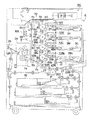
図1は、本発明の感光体の層構成の一例を示す模式図である。 FIG. 1 is a schematic view showing an example of the layer structure of the photoreceptor of the present invention.
図1において、1は導電性支持体、2は感光層、3は中間層、4は電荷発生層、5は電荷輸送層、6は保護層、7は表面処理金属酸化物微粒子を示す。 In FIG. 1, 1 is a conductive support, 2 is a photosensitive layer, 3 is an intermediate layer, 4 is a charge generation layer, 5 is a charge transport layer, 6 is a protective layer, and 7 is a surface-treated metal oxide fine particle.
次に、本発明の感光体を構成する導電性支持体、中間層、感光層(電荷発生層、電荷輸送層)について、及び、感光層を構成する部材について説明する。 Next, the conductive support, intermediate layer, photosensitive layer (charge generation layer, charge transport layer) constituting the photoreceptor of the present invention, and members constituting the photosensitive layer will be described.
(導電性支持体)
本発明で用いられる支持体は、導電性を有するものであればいずれのものでもよく、例えば、アルミニウム、銅、クロム、ニッケル、亜鉛及びステンレスなどの金属をドラムまたはシート状に成形したもの、アルミニウムや銅などの金属箔をプラスチックフィルムにラミネートしたもの、アルミニウム、酸化インジウム及び酸化スズなどをプラスチックフィルムに蒸着したもの、導電性物質を単独またはバインダー樹脂と共に塗布して導電層を設けた金属、プラスチックフィルム及び紙などが挙げられる。
(Conductive support)
The support used in the present invention may be any one as long as it has conductivity, for example, a metal such as aluminum, copper, chromium, nickel, zinc and stainless steel formed into a drum or sheet, aluminum Metal foil such as copper or copper laminated on plastic film, aluminum, indium oxide or tin oxide deposited on plastic film, metal or plastic with conductive layer applied alone or with binder resin Examples include film and paper.
(中間層)
本発明では、導電性支持体と感光層の中間にバリア機能と接着機能を有する中間層を設けることができる。中間層は、カゼイン、ポリビニルアルコール、ニトロセルロース、エチレン−アクリル酸共重合体、ポリアミド、ポリウレタン及びゼラチン等のバインダー樹脂を公知の溶媒に溶解させて浸漬塗布等により形成させることができる。前記バインダー樹脂の中でもアルコール可溶性のポリアミド樹脂が好ましい。
(Middle layer)
In the present invention, an intermediate layer having a barrier function and an adhesive function can be provided between the conductive support and the photosensitive layer. The intermediate layer can be formed by dip coating or the like by dissolving a binder resin such as casein, polyvinyl alcohol, nitrocellulose, ethylene-acrylic acid copolymer, polyamide, polyurethane and gelatin in a known solvent. Among the binder resins, an alcohol-soluble polyamide resin is preferable.
また、中間層には抵抗調整の目的で各種導電性微粒子や金属酸化物粒子を含有させることができる。例えば、アルミナ、酸化亜鉛、酸化チタン、酸化スズ、酸化アンチモン、酸化インジウム、酸化ビスマス等の各種金属酸化物粒子。スズをドープした酸化インジウム、アンチモンをドープした酸化スズ及び酸化ジルコニウムなどの超微粒子を用いることができる。これら金属酸化物粒子を1種類もしくは2種類以上混合して用いることができる。2種類以上混合して用いる場合には、固溶体または融着の形態をとってもよい。この様な金属酸化物粒子は、数平均一次粒径が0.3μm以下のものが好ましく、0.1μm以下のものがより好ましい。 The intermediate layer can contain various conductive fine particles and metal oxide particles for the purpose of adjusting the resistance. For example, various metal oxide particles such as alumina, zinc oxide, titanium oxide, tin oxide, antimony oxide, indium oxide, and bismuth oxide. Ultrafine particles such as indium oxide doped with tin, tin oxide doped with antimony, and zirconium oxide can be used. These metal oxide particles can be used alone or in combination. When two or more kinds are mixed and used, they may take the form of a solid solution or fusion. Such metal oxide particles preferably have a number average primary particle size of 0.3 μm or less, more preferably 0.1 μm or less.
中間層の形成に使用可能な溶媒としては、前述した導電性微粒子や金属酸化物粒子等の無機微粒子を良好に分散させ、ポリアミド樹脂をはじめとするバインダー樹脂を溶解するものが好ましい。具体的には、エタノール、n−プロピルアルコール、イソプロピルアルコール、n−ブタノール、t−ブタノール、sec−ブタノール等の炭素数2〜4のアルコール類が、バインダー樹脂として好ましいとされるポリアミド樹脂に対して良好な溶解性と塗布性能を発現させることから好ましい。また、保存性や無機微粒子の分散性を向上させるために、前記溶媒に対して以下の様な助溶剤を併用することができる。好ましい効果が得られる助溶媒としては、たとえば、メタノール、ベンジルアルコール、トルエン、シクロヘキサノン、テトラヒドロフラン等が挙げられる。 As the solvent that can be used for forming the intermediate layer, a solvent in which inorganic fine particles such as conductive fine particles and metal oxide particles described above are well dispersed and a binder resin such as a polyamide resin is dissolved is preferable. Specifically, with respect to the polyamide resin, alcohols having 2 to 4 carbon atoms such as ethanol, n-propyl alcohol, isopropyl alcohol, n-butanol, t-butanol, sec-butanol and the like are preferable as the binder resin. It is preferable because good solubility and coating performance are exhibited. Further, in order to improve the storage stability and the dispersibility of the inorganic fine particles, the following cosolvent can be used in combination with the solvent. Examples of the co-solvent that can provide a preferable effect include methanol, benzyl alcohol, toluene, cyclohexanone, tetrahydrofuran, and the like.
塗布液形成時のバインダー樹脂濃度は、中間層の膜厚や塗布方式に合わせて適宜選択することができる。また、無機微粒子等を分散させたとき、バインダー樹脂に対する無機微粒子の混合割合は、バインダー樹脂100質量部に対して無機微粒子を20〜400質量部とすることが好ましく、50〜200質量部とすることがより好ましい。 The binder resin concentration at the time of forming the coating solution can be appropriately selected according to the film thickness of the intermediate layer and the coating method. Moreover, when inorganic fine particles etc. are disperse | distributed, it is preferable that the mixing ratio of the inorganic fine particles with respect to binder resin shall be 20-400 mass parts with respect to 100 mass parts of binder resin, and is 50-200 mass parts. It is more preferable.
無機微粒子の分散手段は、超音波分散機、ボールミル、サンドグラインダー、及び、ホモミキサー等が挙げられるがこれらに限定されるものではない。 Examples of the means for dispersing the inorganic fine particles include, but are not limited to, an ultrasonic disperser, a ball mill, a sand grinder, and a homomixer.
また、中間層の乾燥方法は、溶媒の種類や形成する膜厚に応じて公知の乾燥方法を適宜選択することができ、特に熱乾燥が好ましい。 Moreover, the drying method of an intermediate | middle layer can select suitably a well-known drying method according to the kind of solvent and the film thickness to form, and heat drying is especially preferable.
中間層の膜厚は、0.1〜15μmが好ましく、0.3〜10μmがより好ましい。 The thickness of the intermediate layer is preferably from 0.1 to 15 μm, more preferably from 0.3 to 10 μm.
(感光層)
前述した様に、本発明の感光体を構成する感光層は、電荷発生機能と電荷輸送機能を1つの層に付与した単層構造の他に、電荷発生層(CGL)と電荷輸送層(CTL)に感光層の機能を分離させた層構成のものがより好ましい。この様に、機能分離型の層構成とすることにより、繰り返し使用に伴う残留電位の上昇を小さく制御できる他、各種の電子写真特性を目的に合わせて制御し易いメリットがある。負帯電性感光体は中間層の上に電荷発生層(CGL)、その上に電荷輸送層(CTL)を設ける構成をとり、正帯電性感光体は中間層の上に電荷輸送層(CTL)、その上に電荷発生層(CGL)を設ける構成をとる。好ましい感光層の層構成は前記機能分離構造を有する負帯電感光体である。
(Photosensitive layer)
As described above, the photosensitive layer constituting the photoreceptor of the present invention has a charge generation layer (CGL) and a charge transport layer (CTL) in addition to a single layer structure in which a charge generation function and a charge transport function are provided in one layer. And a layer structure in which the functions of the photosensitive layer are separated from each other. As described above, the function-separated type layer structure has an advantage that it is easy to control various electrophotographic characteristics according to the purpose, in addition to being able to control the increase in residual potential with repeated use. The negatively chargeable photoreceptor has a structure in which a charge generation layer (CGL) is provided on an intermediate layer and a charge transport layer (CTL) is provided thereon. The positively chargeable photoreceptor is a charge transport layer (CTL) provided on the intermediate layer. The charge generation layer (CGL) is provided thereon. A preferred layer structure of the photosensitive layer is a negatively charged photoreceptor having the function separation structure.
以下に、感光層の具体例として機能分離型の負帯電感光体の感光層の各層について説明する。 Below, each layer of the photosensitive layer of the function-separated negatively charged photosensitive member will be described as a specific example of the photosensitive layer.
(電荷発生層)
本発明で形成される電荷発生層は、電荷発生物質とバインダー樹脂を含有するもので、電荷発生物質をバインダー樹脂溶液中に分散させてなる塗布液を塗布して形成されたものが好ましい。
(Charge generation layer)
The charge generation layer formed in the present invention contains a charge generation material and a binder resin, and is preferably formed by applying a coating solution in which the charge generation material is dispersed in a binder resin solution.
電荷発生物質は、スーダンレッドやダイアンブルー等のアゾ原料、ピレンキノンやアントアントロン等のキノン顔料、キノシアニン顔料、ペリレン顔料、インジゴ及びチオインジゴ等のインジゴ顔料、フタロシアニン顔料等があり、これらに限定されるものではない。これらの電荷発生物質は単独もしくは公知のバインダー樹脂中に分散させる形態で使用することができる。 Charge generation materials include azo raw materials such as Sudan Red and Diane Blue, quinone pigments such as pyrenequinone and anthanthrone, quinocyanine pigments, perylene pigments, indigo pigments such as indigo and thioindigo, and phthalocyanine pigments is not. These charge generation materials can be used alone or in a form dispersed in a known binder resin.
電荷発生層を形成するバインダー樹脂としては、公知の樹脂を用いることができ、例えば、ポリスチレン樹脂、ポリエチレン樹脂、ポリプロピレン樹脂、アクリル樹脂、メタクリル樹脂、塩化ビニル樹脂、酢酸ビニル樹脂、ポリビニルブチラール樹脂、エポキシ樹脂、ポリウレタン樹脂、フェノール樹脂、ポリエステル樹脂、アルキッド樹脂、ポリカーボネート樹脂、シリコーン樹脂、メラミン樹脂、並びにこれらの樹脂の内2つ以上を含む共重合体樹脂(例えば、塩化ビニル−酢酸ビニル共重合体樹脂、塩化ビニル−酢酸ビニル−無水マレイン酸共重合体樹脂)及びポリ−ビニルカルバゾール樹脂等が挙げられるが、これらに限定されるものではない。 As the binder resin for forming the charge generation layer, known resins can be used. For example, polystyrene resin, polyethylene resin, polypropylene resin, acrylic resin, methacrylic resin, vinyl chloride resin, vinyl acetate resin, polyvinyl butyral resin, epoxy Resin, polyurethane resin, phenol resin, polyester resin, alkyd resin, polycarbonate resin, silicone resin, melamine resin, and copolymer resin containing two or more of these resins (for example, vinyl chloride-vinyl acetate copolymer resin) , Vinyl chloride-vinyl acetate-maleic anhydride copolymer resin) and poly-vinyl carbazole resin, but are not limited thereto.
電荷発生層の形成は、バインダー樹脂を溶媒で溶解した溶液中に分散機を用いて電荷発生物質を分散して塗布液を調製し、塗布液を塗布機で一定の膜厚に塗布し、塗布膜を乾燥して作製することが好ましい。 The charge generation layer is formed by dispersing the charge generation material in a solution obtained by dissolving the binder resin in a solvent using a disperser to prepare a coating solution, and applying the coating solution to a certain film thickness using a coating device. It is preferable to prepare the film by drying.
電荷発生層に使用するバインダー樹脂を溶解し塗布するための溶媒としては、例えば、トルエン、キシレン、メチルエチルケトン、シクロヘキサン、酢酸エチル、酢酸ブチル、メタノール、エタノール、プロパノール、ブタノール、メチルセロソルブ、エチルセロソルブ、テトラヒドロフラン、1−ジオキサン、1,3−ジオキソラン、ピリジン及びジエチルアミン等を挙げられるが、これらに限定されるものではない。 Solvents for dissolving and coating the binder resin used in the charge generation layer include, for example, toluene, xylene, methyl ethyl ketone, cyclohexane, ethyl acetate, butyl acetate, methanol, ethanol, propanol, butanol, methyl cellosolve, ethyl cellosolve, tetrahydrofuran , 1-dioxane, 1,3-dioxolane, pyridine, diethylamine and the like, but are not limited thereto.
電荷発生物質の分散手段としては、超音波分散機、ボールミル、サンドグラインダー及びホモミキサー等が使用できるが、これらに限定されるものではない。 As a means for dispersing the charge generating material, an ultrasonic disperser, a ball mill, a sand grinder, a homomixer, or the like can be used, but is not limited thereto.
バインダー樹脂に対する電荷発生物質の混合割合は、バインダー樹脂100質量部に対して電荷発生物質1〜600質量部が好ましく、50〜500部がより好ましい。電荷発生層の膜厚は、電荷発生物質の特性、バインダー樹脂の特性及び混合割合等により異なるが0.01〜5μmが好ましく、0.05〜3μmがより好ましい。なお、電荷発生層用の塗布液は塗布前に異物や凝集物を濾過することで画像欠陥の発生を防ぐことができる。前記顔料を真空蒸着することによって形成すこともできる。 The mixing ratio of the charge generating material to the binder resin is preferably 1 to 600 parts by weight, more preferably 50 to 500 parts by weight based on 100 parts by weight of the binder resin. The thickness of the charge generation layer varies depending on the characteristics of the charge generation material, the characteristics of the binder resin, the mixing ratio, and the like, but is preferably 0.01 to 5 μm, more preferably 0.05 to 3 μm. It should be noted that the coating solution for the charge generation layer can prevent the occurrence of image defects by filtering foreign matter and aggregates before coating. The pigment can also be formed by vacuum deposition.
(電荷輸送層)
本発明で形成される電荷輸送層は、少なくとも層内に電荷輸送物質とバインダー樹脂を含有するものであり、電荷輸送物質をバインダー樹脂溶液中に溶解、塗布して形成される。
(Charge transport layer)
The charge transport layer formed in the present invention contains at least a charge transport material and a binder resin in the layer, and is formed by dissolving and coating the charge transport material in a binder resin solution.
電荷輸送物質は、公知の化合物を用いることが可能で、たとえば、以下の様なものが挙げられる。すなわち、カルバゾール誘導体、オキサゾール誘導体、オキサジアゾール誘導体、チアゾール誘導体、チアジアゾール誘導体、トリアゾール誘導体、イミダゾール誘導体、イミダゾロン誘導体、イミダゾリジン誘導体、ビスイミダゾリジン誘導体、スチリル化合物、ヒドラゾン化合物、ピラゾリン化合物、オキサゾロン誘導体、ベンズイミダゾール誘導体、キナゾリン誘導体、ベンゾフラン誘導体、アクリジン誘導体、フェナジン誘導体、アミノスチルベン誘導体、トリアリールアミン誘導体、フェニレンジアミン誘導体、スチルベン誘導体、ベンジジン誘導体、ポリ−N−ビニルカルバゾール、ポリ−1−ビニルピレン及びポリ−9−ビニルアントラセン等。これらの化合物を単独あるいは2種類以上混合して使用することができる。 As the charge transport material, a known compound can be used, and examples thereof include the following. Carbazole derivatives, oxazole derivatives, oxadiazole derivatives, thiazole derivatives, thiadiazole derivatives, triazole derivatives, imidazole derivatives, imidazolone derivatives, imidazolidine derivatives, bisimidazolidine derivatives, styryl compounds, hydrazone compounds, pyrazoline compounds, oxazolone derivatives, benz Imidazole derivatives, quinazoline derivatives, benzofuran derivatives, acridine derivatives, phenazine derivatives, aminostilbene derivatives, triarylamine derivatives, phenylenediamine derivatives, stilbene derivatives, benzidine derivatives, poly-N-vinylcarbazole, poly-1-vinylpyrene and poly-9 -Vinylanthracene and the like. These compounds can be used alone or in admixture of two or more.
また、電荷輸送層用のバインダー樹脂は公知の樹脂を用いることが可能で、たとえば、以下の様なものがある。すなわち、ポリカーボネート樹脂、ポリアクリレート樹脂、ポリエステル樹脂、ポリスチレン樹脂、スチレン−アクリルニトリル共重合体樹脂、ポリメタクリル酸エステル樹脂、スチレン−メタクリル酸エステル共重合体樹脂等が挙げられる。これらの中でもポリカーボネート樹脂が好ましく、さらに、ビスフェノールA(BPA)、ビスフェノールZ(BPZ)、ジメチルBPA、BPA−ジメチルBPA共重合体等のタイプのポリカーボネート樹脂が耐クラック性、耐磨耗性、帯電特性の視点から好ましいものである。 Further, a known resin can be used as the binder resin for the charge transport layer, and examples thereof include the following. That is, polycarbonate resin, polyacrylate resin, polyester resin, polystyrene resin, styrene-acrylonitrile copolymer resin, polymethacrylic acid ester resin, styrene-methacrylic acid ester copolymer resin, and the like. Of these, polycarbonate resins are preferable, and polycarbonate resins of the types such as bisphenol A (BPA), bisphenol Z (BPZ), dimethyl BPA, and BPA-dimethyl BPA copolymer are crack resistant, wear resistant, and charging characteristics. From the viewpoint of
電荷輸送層は塗布法に代表される公知の方法で形成することが可能であり、たとえば、塗布法では、バインダー樹脂と電荷輸送物質を溶解して塗布液を調製し、塗布液を一定の膜厚で塗布後、乾燥処理することにより所望の電荷輸送層を形成することができる。 The charge transport layer can be formed by a known method typified by a coating method. For example, in the coating method, a binder resin and a charge transport material are dissolved to prepare a coating solution, and the coating solution is formed into a certain film. A desired charge transport layer can be formed by drying after coating with a thickness.
上記バインダー樹脂と電荷輸送物質を溶解する溶媒としては、例えば、トルエン、キシレン、メチルエチルケトン、シクロヘキサノン、酢酸エチル、酢酸ブチル、メタノール、エタノール、プロパノール、ブタノール、テトラヒドロフラン、1,4−ジオキサン、1,3−ジオキソラン等が挙げられる。なお、電荷輸送層形成用の塗布液を作製する際に使用する溶媒は上記のものに限定されるものではない。 Examples of the solvent for dissolving the binder resin and the charge transport material include toluene, xylene, methyl ethyl ketone, cyclohexanone, ethyl acetate, butyl acetate, methanol, ethanol, propanol, butanol, tetrahydrofuran, 1,4-dioxane, 1,3- And dioxolane. The solvent used when preparing the coating liquid for forming the charge transport layer is not limited to the above.
バインダー樹脂と電荷輸送物質の混合比率は、バインダー樹脂100質量部に対して電荷輸送物質を10〜500質量部とすることが好ましく、20〜100質量部とすることがより好ましい。 The mixing ratio of the binder resin and the charge transport material is preferably 10 to 500 parts by weight, and more preferably 20 to 100 parts by weight with respect to 100 parts by weight of the binder resin.
電荷輸送層の厚さは、電荷輸送物質やバインダー樹脂の特性、及び、これらの混合比等により異なるが、5〜40μmが好ましく、10〜30μmがより好ましい。 The thickness of the charge transport layer varies depending on the characteristics of the charge transport material and the binder resin, the mixing ratio thereof, and the like, but is preferably 5 to 40 μm, and more preferably 10 to 30 μm.
電荷輸送層中には、公知の酸化防止剤を添加することが可能で、例えば特開2000−305291号公報記載の酸化防止剤が使用できる。 In the charge transport layer, a known antioxidant can be added. For example, an antioxidant described in JP-A-2000-305291 can be used.
(感光体の塗布方法)
本発明の感光体を構成する中間層、電荷発生層、電荷輸送層、保護層等の各層は公知の塗布方法により形成することができる。具体的には、浸漬コーティング法、スプレーコーティング法、スピンナーコーティング法、ビードコーティング法、ブレードコーティング法、ビームコーティング法、円形量規制型塗布法等が挙げられる。
(Photoreceptor application method)
Each layer such as an intermediate layer, a charge generation layer, a charge transport layer and a protective layer constituting the photoreceptor of the present invention can be formed by a known coating method. Specific examples include a dip coating method, a spray coating method, a spinner coating method, a bead coating method, a blade coating method, a beam coating method, and a circular amount-regulating coating method.
円形量規制型塗布方法については、特開昭58−189061号公報に記載されている。 The circular amount regulation type coating method is described in JP-A-58-189061.
≪画像形成装置≫
本発明に係る画像形成装置について説明する。
≪Image forming device≫
An image forming apparatus according to the present invention will be described.
本発明の効果を実現する画像形成装置は、
(1)少なくとも本発明の保護層を有する電子写真感光体、
(2)前述した電子写真感光体表面を帯電する帯電手段、
(3)帯電手段により帯電された電子写真感光体表面に像露光を行い潜像形成を行う露光手段、
(4)露光手段により形成された潜像を顕像化してトナー画像を形成する現像手段、
(5)現像手段により電子写真感光体表面に形成されたトナー画像を用紙等の転写媒体あるいは転写ベルト上に転写する転写手段、を有するものである。
An image forming apparatus that realizes the effects of the present invention is as follows.
(1) An electrophotographic photosensitive member having at least the protective layer of the present invention,
(2) Charging means for charging the surface of the electrophotographic photosensitive member described above,
(3) An exposure unit that performs image exposure on the surface of the electrophotographic photosensitive member charged by the charging unit to form a latent image;
(4) developing means for visualizing the latent image formed by the exposure means to form a toner image;
(5) The image forming apparatus includes a transfer unit that transfers the toner image formed on the surface of the electrophotographic photosensitive member by the developing unit onto a transfer medium such as paper or a transfer belt.
尚、電子写真感光体を帯電させる帯電手段では非接触帯電装置を用いることが好ましい。非接触帯電装置としては、コロナ帯電装置、コロトロン帯電装置、スコロトロン帯電装置を挙げることができる。 Note that a non-contact charging device is preferably used as the charging means for charging the electrophotographic photosensitive member. Examples of the non-contact charging device include a corona charging device, a corotron charging device, and a scorotron charging device.
図2は、本発明の実施形態のひとつを示すカラー画像形成装置の一例を説明する断面構成図である。 FIG. 2 is a cross-sectional configuration diagram illustrating an example of a color image forming apparatus showing one of the embodiments of the present invention.
このカラー画像形成装置は、タンデム型カラー画像形成装置と称せられるもので、4組の画像形成部(画像形成ユニット)10Y、10M、10C、10Bkと、無端ベルト状中間転写体ユニット7と、給紙搬送手段21及び定着手段24とから成る。画像形成装置の本体Aの上部には、原稿画像読み取り装置SCが配置されている。
This color image forming apparatus is called a tandem type color image forming apparatus, and includes four sets of image forming units (image forming units) 10Y, 10M, 10C, and 10Bk, an endless belt-shaped intermediate
イエロー色の画像を形成する画像形成部10Yは、第1の像担持体としてのドラム状の感光体1Yの周囲に配置された帯電手段(帯電工程)2Y、露光手段(露光工程)3Y、現像手段(現像工程)4Y、一次転写手段(一次転写工程)としての一次転写ローラ5Y、クリーニング手段6Yを有する。マゼンタ色の画像を形成する画像形成部10Mは、第1の像担持体としてのドラム状の感光体1M、帯電手段2M、露光手段3M、現像手段4M、一次転写手段としての一次転写ローラ5M、クリーニング手段6Mを有する。シアン色の画像を形成する画像形成部10Cは、第1の像担持体としてのドラム状の感光体1C、帯電手段2C、露光手段3C、現像手段4C、一次転写手段としての一次転写ローラ5C、クリーニング手段6Cを有する。黒色画像を形成する画像形成部10Bkは、第1の像担持体としてのドラム状の感光体1Bk、帯電手段2Bk、露光手段3Bk、現像手段4Bk、一次転写手段としての一次転写ローラ5Bk、クリーニング手段6Bkを有する。
The
前記4組の画像形成ユニット10Y、10M、10C、10Bkは、感光体ドラム1Y、1M、1C、1Bkを中心に、回転する帯電手段2Y、2M、2C、2Bkと、像露光手段3Y、3M、3C、3Bkと、回転する現像手段4Y、4M、4C、4Bk、及び、感光体ドラム1Y、1M、1C、1Bkをクリーニングするクリーニング手段6Y、6M、6C、6Bkより構成されている。
The four sets of
前記画像形成ユニット10Y、10M、10C、10Bkは、感光体1Y、1M、1C、1Bkにそれぞれ形成するトナー画像の色が異なるだけで、同じ構成であり、画像形成ユニット10Yを例にして詳細に説明する。
The
画像形成ユニット10Yは、像形成体である感光体ドラム1Yの周囲に、帯電手段2Y(以下、単に帯電手段2Y、あるいは、帯電器2Yという)、露光手段3Y、現像手段4Y、クリーニング手段6Y(以下、単にクリーニング手段6Y、あるいは、クリーニングブレード6Yという)を配置し、感光体ドラム1Y上にイエロー(Y)のトナー画像を形成するものである。また、本実施の形態においては、この画像形成ユニット10Yのうち、少なくとも感光体ドラム1Y、帯電手段2Y、現像手段4Y、クリーニング手段6Yを一体化するように設けている。
The
帯電手段2Yは、感光体ドラム1Yに対して一様な電位を与える手段であって、本実施の形態においては、感光体ドラム1Yにコロナ放電型の帯電器2Yが用いられている。
The charging unit 2Y is a unit that applies a uniform potential to the
像露光手段3Yは、帯電器2Yによって一様な電位を与えられた感光体ドラム1Y上に、画像信号(イエロー)に基づいて露光を行い、イエローの画像に対応する静電潜像を形成する手段であって、この露光手段3Yとしては、感光体ドラム1Yの軸方向にアレイ状に発光素子を配列したLEDと結像素子(商品名;セルフォックレンズ)とから構成されるもの、あるいは、レーザ光学系などが用いられる。
The image exposure means 3Y performs exposure based on the image signal (yellow) on the
本発明の画像形成装置としては、上述の感光体と、現像器、クリーニング器等の構成要素をプロセスカートリッジ(画像形成ユニット)として一体に結合して構成し、この画像形成ユニットを装置本体に対して着脱自在に構成しても良い。又、帯電器、像露光器、現像器、転写又は分離器、及びクリーニング器の少なくとも1つを感光体とともに一体に支持してプロセスカートリッジ(画像形成ユニット)を形成し、装置本体に着脱自在の単一画像形成ユニットとし、装置本体のレールなどの案内手段を用いて着脱自在の構成としても良い。 The image forming apparatus of the present invention is configured by integrally combining the above-described photosensitive member and components such as a developing device and a cleaning device as a process cartridge (image forming unit), and this image forming unit is connected to the apparatus main body. It may be configured to be detachable. In addition, at least one of a charging device, an image exposure device, a developing device, a transfer or separation device, and a cleaning device is integrally supported together with a photosensitive member to form a process cartridge (image forming unit), which is detachable from the apparatus main body. A single image forming unit may be detachable using guide means such as a rail of the apparatus main body.
無端ベルト状中間転写体ユニット7は、複数のローラにより巻回され、回動可能に支持された半導電性エンドレスベルト状の第2の像担持体としての無端ベルト状中間転写体70を有する。
The endless belt-like intermediate
画像形成ユニット10Y、10M、10C、10Bkより形成された各色の画像は、一次転写手段としての一次転写ローラ5Y、5M、5C、5Bkにより、回動する無端ベルト状中間転写体70上に逐次転写されて、合成されたカラー画像が形成される。給紙カセット20内に収容された転写材(定着された最終画像を担持する支持体:例えば普通紙、透明シート等)としての転写材Pは、給紙手段21により給紙され、複数の中間ローラ22A、22B、22C、22D、レジストローラ23を経て、二次転写手段としての二次転写ローラ5bに搬送され、転写材P上に二次転写してカラー画像が一括転写される。カラー画像が転写された転写材Pは、定着手段24により定着処理され、排紙ローラ25に挟持されて機外の排紙トレイ26上に載置される。ここで、中間転写体や転写材等の感光体上に形成されたトナー画像の転写支持体を総称して転写媒体という。
Each color image formed by the
一方、二次転写手段としての二次転写ローラ5bにより転写材Pにカラー画像を転写した後、転写材Pを曲率分離した無端ベルト状中間転写体70は、クリーニング手段6bにより残留トナーが除去される。
On the other hand, after the color image is transferred to the transfer material P by the
画像形成処理中、一次転写ローラ5Bkは常時、感光体1Bkに当接している。他の一次転写ローラ5Y、5M、5Cはカラー画像形成時にのみ、それぞれ対応する感光体1Y、1M、1Cに当接する。
During the image forming process, the primary transfer roller 5Bk is always in contact with the photoreceptor 1Bk. The other
二次転写ローラ5bは、ここを転写材Pが通過して二次転写が行われる時にのみ、無端ベルト状中間転写体70に当接する。
The
また、装置本体Aから筐体8を支持レール82L、82Rを介して引き出し可能にしてある。 Further, the housing 8 can be pulled out from the apparatus main body A through the support rails 82L and 82R.
筐体8は、画像形成部10Y、10M、10C、10Bkと、無端ベルト状中間転写体ユニット7とから成る。
The housing 8 includes
画像形成部10Y、10M、10C、10Bkは、垂直方向に縦列配置されている。感光体1Y、1M、1C、1Bkの図示左側方には無端ベルト状中間転写体ユニット7が配置されている。無端ベルト状中間転写体ユニット7は、ローラ71、72、73、74を巻回して回動可能な無端ベルト状中間転写体70、一次転写ローラ5Y、5M、5C、5Bk、及びクリーニング手段6bとから成る。
The
以下に実施例を挙げて本発明を具体的に説明するが、本発明はこれらに限定されるものではない。 EXAMPLES The present invention will be specifically described below with reference to examples, but the present invention is not limited to these examples.
≪表面処理金属酸化物微粒子の作製≫
(表面処理金属酸化物微粒子1の作製)
金属酸化物微粒子として数平均一次粒径20nmの「酸化スズ」100質量部、重合性表面処理剤として「例示化合物S−12」30質量部メチルエチルケトン1000質量部を湿式サンドミル(径0.5mmのアルミナビーズ)に入れ、30℃にて6時間混合、その後、メチルエチルケトンとアルミナビーズを濾別し、60℃にて乾燥し「表面処理金属酸化物微粒子1」を調製した。
≪Preparation of surface-treated metal oxide fine particles≫
(Preparation of surface-treated metal oxide fine particles 1)
100 parts by mass of “tin oxide” having a number average primary particle size of 20 nm as metal oxide fine particles and 30 parts by mass of “Exemplary Compound S-12” as a polymerizable surface treatment agent are mixed with 1000 parts by mass of methyl ethyl ketone. Bead) and mixed at 30 ° C. for 6 hours, and then methyl ethyl ketone and alumina beads were separated by filtration and dried at 60 ° C. to prepare “surface-treated metal
(表面処理金属酸化物微粒子2の作製)
表面処理金属酸化物微粒子1の作製において、金属酸化物微粒子として数平均一次粒径30nmの「アルミナ」100質量部を用いた他は同様にして、「表面処理金属酸化物微粒子2」を作製した。
(Preparation of surface-treated metal oxide fine particles 2)
In the production of the surface-treated metal
(表面処理金属酸化物微粒子3の作製)
表面処理金属酸化物微粒子1の作製において、金属酸化物微粒子として数平均一次粒径30nmの「二酸化チタン」を用いた他は同様にして「表面処理金属酸化物微粒子3」を作製した。
(Preparation of surface-treated metal oxide fine particles 3)
In the production of the surface-treated metal
(表面処理金属酸化物微粒子4の作製)
表面処理金属酸化物微粒子1の作製において、重合性表面処理剤として「例示化合物15」を用いた他は同様にして「表面処理金属酸化物微粒子4」を作製した。
(Preparation of surface-treated metal oxide fine particles 4)
In the production of the surface-treated metal
≪感光体1の作製≫
(導電性支持体の準備)
円筒形アルミニウム支持体の表面を切削加工し、表面粗さRz=1.5(μm)の導電性支持体を準備した。
<< Production of
(Preparation of conductive support)
The surface of the cylindrical aluminum support was cut to prepare a conductive support having a surface roughness Rz = 1.5 (μm).
(中間層の形成)
下記組成の分散液を同じ混合溶媒にて2倍に希釈し、一夜静置後に濾過(フィルター;日本ポール社製リジメッシュ5μmフィルター使用)し、中間層塗布液を作製した。
(Formation of intermediate layer)
A dispersion having the following composition was diluted twice with the same mixed solvent, allowed to stand overnight, and then filtered (filter; using a lysh mesh 5 μm filter manufactured by Nippon Pole Co., Ltd.) to prepare an intermediate layer coating solution.
ポリアミド樹脂CM8000(東レ社製) 1質量部
酸化チタンSMT500SAS(テイカ社製) 3質量部
メタノール 10質量部
分散機としてサンドミルを用いて、バッチ式で10時間の分散を行った。
Polyamide resin CM8000 (manufactured by Toray Industries, Inc.) 1 part by mass Titanium oxide SMT500SAS (manufactured by Teica) 3 parts by mass Methanol 10 parts by mass Using a sand mill as a disperser, dispersion was carried out for 10 hours in a batch system.
上記塗布液を前記導電性支持体上に、乾燥膜厚2μmとなるよう浸漬塗布法で塗布、乾燥して「中間層」を形成した。 The said coating liquid was apply | coated and dried by the dip coating method so that it might become a dry film thickness of 2 micrometers on the said electroconductive support body, and the "intermediate layer" was formed.
(電荷発生層の形成)
下記組成を混合し、サンドミルを用いて10時間分散し、電荷発生層塗布液を調製した。
(Formation of charge generation layer)
The following compositions were mixed and dispersed for 10 hours using a sand mill to prepare a charge generation layer coating solution.
電荷発生物質:チタニルフタロシアニン顔料(Cu−Kα特性X線回折スペクトル測定で、少なくとも27.3°の位置に最大回折ピークを有するチタニルフタロシアニン顔料) 20質量部
ポリビニルブチラール樹脂(#6000−C:電気化学工業社製) 10質量部
酢酸t−ブチル 700質量部
4−メトキシ−4−メチル−2−ペンタノン 300質量部
この電荷発生層塗布液を前記中間層の上に浸漬塗布法で塗布、乾燥して、乾燥膜厚0.3μmの「電荷発生層」を形成した。
Charge generation material: titanyl phthalocyanine pigment (titanyl phthalocyanine pigment having a maximum diffraction peak at a position of at least 27.3 ° by Cu-Kα characteristic X-ray diffraction spectrum measurement) 20 parts by mass Polyvinyl butyral resin (# 6000-C: electrochemical 10 parts by mass t-butyl acetate 700 parts by mass 4-methoxy-4-methyl-2-pentanone 300 parts by mass This charge generation layer coating solution is applied onto the intermediate layer by a dip coating method and dried. Then, a “charge generation layer” having a dry film thickness of 0.3 μm was formed.
(電荷輸送層の形成)
下記組成を混合、溶解して電荷輸送層塗布液を調製した。
(Formation of charge transport layer)
The following composition was mixed and dissolved to prepare a charge transport layer coating solution.
電荷輸送物質(4,4′−ジメチル−4″−(β−フェニルスチリル)トリフェニルアミン) 225質量部
バインダー:ポリカーボネート(Z300:三菱ガス化学社製) 300質量部
酸化防止剤(Irganox1010:BASFジャパン社製) 6質量部
THF 1600質量部
トルエン 400質量部
シリコーンオイル(KF−54:信越化学社製) 1質量部
この電荷輸送層塗布液を前記電荷発生層の上に円形量規制型塗布機を用いて塗布し、乾燥して乾燥膜厚20μmの「電荷輸送層」を形成した。
Charge transport material (4,4′-dimethyl-4 ″-(β-phenylstyryl) triphenylamine) 225 parts by mass Binder: Polycarbonate (Z300: manufactured by Mitsubishi Gas Chemical Company) 300 parts by mass Antioxidant (Irganox 1010: BASF Japan) 6 parts by mass THF 1600 parts by mass Toluene 400 parts by mass Silicone oil (KF-54: manufactured by Shin-Etsu Chemical Co., Ltd.) 1 part by mass This charge transport layer coating solution is placed on the charge generation layer with a circular amount regulating type coating machine. It was applied and dried to form a “charge transport layer” having a dry film thickness of 20 μm.
(保護層の形成)
下記組成を溶解、分散して表面層塗布液を調製した。
(Formation of protective layer)
The following composition was dissolved and dispersed to prepare a surface layer coating solution.
表面処理金属酸化物微粒子1 100質量部
重合性化合物(例示化合物M1) 100質量部
重合開始剤(イルガキュアー819:BASFジャパン社製) 7.5質量部
sec−ブチルアルコール 360質量部
メチルイソプロピルケトン 90質量部
この表面層塗布液を上記電荷輸送層の上に円形量規制型塗布装置を用いて塗布し、表面層を形成した。形成した表面層を乾燥後、メタルハライドランプを用いて窒素気流下、光源から感光体表面までの距離を100mmに設置し、ランプ出力4kWで紫外線を1分間照射して、乾燥膜厚3.5μmの「表面層」を形成し、「感光体1」を作製した。
Surface-treated metal
こうして作製した感光体1の電荷輸送層及び保護層を剥離した。剥離した膜のうち0.1gについて、前述したように、ガスクロマトグラフ質量分析計(GC/HP6890及びMS/HP5973:アジレント・テクノロジー社製)による分析を行った。GCカラムは、DB−624(内径:0.25mm、長さ:30m、膜厚:1.40μm)を用いて、GCカラムオーブン温度を40℃で2分保持し、10℃/分の速度で100℃まで昇温後、20℃/分で230℃まで昇温し5分保持して測定した。この時の、スキャン質量範囲m/zは20−100であり、HS条件は、130℃、30minで行った。
The charge transport layer and the protective layer of the
キャリアガスは高純度He(99.99質量%)を用い、流量1.2ml/min、スプリット比20:1、HSは130℃、30分の加熱を行い、ヘッドスペース法により気相が含むアルコール及びケトンの合計濃度を溶媒量として測定したところ、アルコール及びケトンの合計での溶媒量は47ppmであった。検量線は標準試料を用いた測定により作製した。 The carrier gas is high purity He (99.99% by mass), the flow rate is 1.2 ml / min, the split ratio is 20: 1, HS is heated at 130 ° C. for 30 minutes, and the alcohol contained in the gas phase by the headspace method. When the total concentration of alcohol and ketone was measured as the amount of solvent, the total amount of solvent of alcohol and ketone was 47 ppm. The calibration curve was prepared by measurement using a standard sample.
≪感光体2〜20の作製≫
感光体1において、表面層塗布液の溶媒種及び量の変更、乾燥膜厚の量の変更、保護層塗布後の光照射前後の乾燥条件を変更するなどし、溶媒量を変化させ、感光体2〜20を作製した。各感光体1〜20の組成、膜厚、乾燥条件、含有溶媒量を下記表1に記載する。ここで感光体1〜16は本発明の感光体、感光体17〜20は比較用の感光体とした。
<< Production of photoconductors 2-20 >>
In the
≪評価方法と判定基準≫
以上のようにして作製した感光体について、以下のようにして評価を行った。
≪Evaluation method and criteria≫
The photoconductor produced as described above was evaluated as follows.
(感光体表面の耐摩耗性)
本発明の電子写真感光体をコニカミノルタビジネステクノロジーズ社製「bizhub PRO C6500」(波長780nmのレーザ露光・反転現像・中間転写体のタンデム方式カラー複合機)に搭載し、(30℃、85%RH)でイエロー(Y)、マゼンタ(M)、シアン(C)、ブラック(Bk)各色印字面積率5%のA4版画像をA4版中性紙に100万枚の画出しを行い、初期膜厚と100万枚後の膜厚さで評価した。感光層の膜厚は均一膜厚部分(感光体の両端は膜厚が不均一になりやすいので、少なくとも両端3cmは除く)をランダムに10ヶ所測定し、その平均値を感光層の膜厚とする。膜厚測定器は渦電流方式の膜厚測定器EDDY560C(HELMUT FISCHER GMBTE CO社製)を用いて行い、実写試験前後の感光層膜厚の差を膜厚減耗量とする。
(Abrasion resistance of photoreceptor surface)
The electrophotographic photosensitive member of the present invention is mounted on “bizhub PRO C6500” (tandem color composite machine of laser exposure / reversal development / intermediate transfer body at a wavelength of 780 nm) manufactured by Konica Minolta Business Technologies, Inc. (30 ° C., 85% RH). ) Yellow (Y), magenta (M), cyan (C), and black (Bk) A4 plate images of 5% color printing area ratio are printed on neutral paper of A4 plate, and the initial film The thickness and the film thickness after 1 million sheets were evaluated. The photosensitive layer has a uniform thickness (measured at 10 locations at random, excluding at least 3 cm at both ends because the film thickness tends to be non-uniform at both ends of the photoconductor). To do. The film thickness measuring device is an eddy current film thickness measuring device EDDY560C (manufactured by HELMUT FISCHER GMBTE CO), and the difference in the photosensitive layer thickness before and after the actual shooting test is defined as the film thickness depletion amount.
具体的には下記α値にて評価した。 Specifically, the following α value was evaluated.
α値={(深さ方向の膜厚減耗量[μm])/ドラムの総回転数}×100000
すなわち、α値が小さいほど、耐摩耗性を有する。
α value = {(thickness loss in the depth direction [μm]) / total number of revolutions of drum} × 100,000
That is, the smaller the α value, the higher the wear resistance.
(濃度段差)
上記複合機でA3中性紙全面にハーフトーン画像(マクベス濃度計で平均相対反射濃度0.4)を複写し、A3紙面(縦297mm×横420mm)の隅から横方向180mmの位置で縦方向の端から33mm間隔の計8点をそれぞれa1、a2〜a8とし、隅から横方向195mmの位置で縦方向の端から33mm間隔の計8点を同様にb1、b2〜b8とした時に、マクベス濃度計にて各点の反射濃度を測定した。これらのa1とb1の測定値の差、a2とb2の測定値の差と順に計8つの組み合わせの測定値の差を評価した。
(Density step)
A halftone image (average relative reflection density 0.4 by Macbeth densitometer) is copied on the entire surface of A3 neutral paper with the above-mentioned multi-function machine, and longitudinally at a position 180 mm laterally from the corner of the A3 paper (vertical 297 mm × width 420 mm). Macbeth is defined as a total of 8 points at intervals of 33 mm from the end of the frame, a1 and a2 to a8, respectively, and a total of 8 points at intervals of 195 mm in the horizontal direction from the corner and 33 mm from the end of the vertical direction is b1, b2 to b8. The reflection density at each point was measured with a densitometer. The difference between the measurement values of a1 and b1, the difference between the measurement values of a2 and b2, and the difference of the measurement values of a total of eight combinations were evaluated.
◎:測定値の差の最大値が0.01未満(良好)
○:測定値の差の最大値が0.01以上0.02未満(実用上問題なし)
△:測定値の差の最大値が0.02以上0.04未満(実用化可能)
×:測定値の差の最大値が0.04以上(実用上問題あり)
A: Maximum difference in measured values is less than 0.01 (good)
○: The maximum difference between measured values is 0.01 or more and less than 0.02 (no problem in practical use)
Δ: The maximum difference between the measured values is 0.02 or more and less than 0.04 (practical use)
×: The maximum difference between the measured values is 0.04 or more (there is a problem in practical use)
表2の結果から明らかなように本発明の感光体1〜16は比較用の感光体17〜20に比べて、耐摩耗性、濃度段差の両特性において極めて優れた感光体であることが分かる。
As is apparent from the results in Table 2, it can be seen that the
1 導電性支持体
2 感光層
3 中間層
4 電荷発生層
5 電荷輸送層
6 保護層
7 表面処理金属酸化物微粒子
1Y、1M、1C、1Bk 感光体ドラム
2Y、2M、2C、2Bk 帯電手段
3Y、3M、3C、3Bk 像露光手段
4Y、4M、4C、4Bk 現像手段
6Y、6M、6C、6Bk クリーニング手段
10Y、10M、10C、10Bk 画像形成ユニット
DESCRIPTION OF
Claims (5)
Priority Applications (1)
| Application Number | Priority Date | Filing Date | Title |
|---|---|---|---|
| JP2011116676A JP5772217B2 (en) | 2011-05-25 | 2011-05-25 | Electrophotographic photoreceptor |
Applications Claiming Priority (1)
| Application Number | Priority Date | Filing Date | Title |
|---|---|---|---|
| JP2011116676A JP5772217B2 (en) | 2011-05-25 | 2011-05-25 | Electrophotographic photoreceptor |
Publications (2)
| Publication Number | Publication Date |
|---|---|
| JP2012247474A true JP2012247474A (en) | 2012-12-13 |
| JP5772217B2 JP5772217B2 (en) | 2015-09-02 |
Family
ID=47467987
Family Applications (1)
| Application Number | Title | Priority Date | Filing Date |
|---|---|---|---|
| JP2011116676A Expired - Fee Related JP5772217B2 (en) | 2011-05-25 | 2011-05-25 | Electrophotographic photoreceptor |
Country Status (1)
| Country | Link |
|---|---|
| JP (1) | JP5772217B2 (en) |
Cited By (2)
| Publication number | Priority date | Publication date | Assignee | Title |
|---|---|---|---|---|
| JP2019035804A (en) * | 2017-08-10 | 2019-03-07 | キヤノン株式会社 | Electrophotographic photosensitive member, production method of electrophotographic photosensitive member, process cartridge, and electrophotographic apparatus |
| JP2021128347A (en) * | 2018-01-19 | 2021-09-02 | 富士電機株式会社 | Electrophotographic photoreceptor, method for manufacturing the same, and electrophotographic device |
Citations (4)
| Publication number | Priority date | Publication date | Assignee | Title |
|---|---|---|---|---|
| JP2000267308A (en) * | 1999-03-19 | 2000-09-29 | Mitsubishi Chemicals Corp | Electrophotographic photoreceptor and electrophotographic device using same |
| JP2004334246A (en) * | 1999-03-02 | 2004-11-25 | Ricoh Co Ltd | Electrophotographic photoreceptor and electrophotographic apparatus |
| JP2009282281A (en) * | 2008-05-22 | 2009-12-03 | Konica Minolta Business Technologies Inc | Electrophotographic photoreceptor and image forming method using the same |
| JP2010224529A (en) * | 2009-02-24 | 2010-10-07 | Konica Minolta Business Technologies Inc | Electrophotographic photoreceptor, image forming apparatus, and process cartridge |
-
2011
- 2011-05-25 JP JP2011116676A patent/JP5772217B2/en not_active Expired - Fee Related
Patent Citations (4)
| Publication number | Priority date | Publication date | Assignee | Title |
|---|---|---|---|---|
| JP2004334246A (en) * | 1999-03-02 | 2004-11-25 | Ricoh Co Ltd | Electrophotographic photoreceptor and electrophotographic apparatus |
| JP2000267308A (en) * | 1999-03-19 | 2000-09-29 | Mitsubishi Chemicals Corp | Electrophotographic photoreceptor and electrophotographic device using same |
| JP2009282281A (en) * | 2008-05-22 | 2009-12-03 | Konica Minolta Business Technologies Inc | Electrophotographic photoreceptor and image forming method using the same |
| JP2010224529A (en) * | 2009-02-24 | 2010-10-07 | Konica Minolta Business Technologies Inc | Electrophotographic photoreceptor, image forming apparatus, and process cartridge |
Cited By (3)
| Publication number | Priority date | Publication date | Assignee | Title |
|---|---|---|---|---|
| JP2019035804A (en) * | 2017-08-10 | 2019-03-07 | キヤノン株式会社 | Electrophotographic photosensitive member, production method of electrophotographic photosensitive member, process cartridge, and electrophotographic apparatus |
| JP2021128347A (en) * | 2018-01-19 | 2021-09-02 | 富士電機株式会社 | Electrophotographic photoreceptor, method for manufacturing the same, and electrophotographic device |
| JP7180717B2 (en) | 2018-01-19 | 2022-11-30 | 富士電機株式会社 | Electrophotographic photoreceptor, manufacturing method thereof, and electrophotographic apparatus |
Also Published As
| Publication number | Publication date |
|---|---|
| JP5772217B2 (en) | 2015-09-02 |
Similar Documents
| Publication | Publication Date | Title |
|---|---|---|
| JP5664538B2 (en) | Electrophotographic photoreceptor | |
| JP6024247B2 (en) | Electrophotographic photosensitive member, method for producing electrophotographic photosensitive member, electrophotographic image forming method, and electrophotographic image forming apparatus | |
| JP5929882B2 (en) | Organic photoreceptor, image forming apparatus and image forming method | |
| JP6146432B2 (en) | Electrophotographic photoreceptor | |
| JP6093217B2 (en) | Electrophotographic photoreceptor and image forming apparatus | |
| JP2012123238A (en) | Electrophotographic photoreceptor | |
| JP6048461B2 (en) | Electrophotographic photosensitive member, electrophotographic image forming method, and electrophotographic image forming apparatus | |
| JP6060531B2 (en) | Organic photoconductor manufacturing method and image forming apparatus | |
| JP5968585B2 (en) | Method for producing electrophotographic photosensitive member | |
| JP5915396B2 (en) | Electrophotographic photosensitive member, electrophotographic image forming method, and electrophotographic image forming apparatus | |
| JP6197668B2 (en) | Electrophotographic photoreceptor and method for producing the same | |
| JP6447254B2 (en) | Electrophotographic photosensitive member and electrophotographic image forming apparatus | |
| JP2012078620A (en) | Electrophotographic photoreceptor | |
| JP6451294B2 (en) | Electrophotographic photoreceptor and image forming apparatus having the same | |
| JP5772217B2 (en) | Electrophotographic photoreceptor | |
| JP6056306B2 (en) | Electrophotographic photosensitive member, and image forming apparatus and image forming method using the same | |
| JP6060706B2 (en) | Organic photoreceptor and image forming apparatus | |
| JP6720750B2 (en) | Electrophotographic photoreceptor, manufacturing method thereof, and electrophotographic image forming apparatus | |
| JP2012173511A (en) | Electrophotographic photoreceptor | |
| JP2012098591A (en) | Electrophotographic photoreceptor | |
| JP6086023B2 (en) | Electrophotographic photosensitive member, electrophotographic image forming method, and electrophotographic image forming apparatus | |
| JP2011186120A (en) | Organic photoreceptor, image forming apparatus and process cartridge | |
| JP2012098500A (en) | Electrophotographic photoreceptor | |
| JP6405783B2 (en) | Electrophotographic photosensitive member, electrophotographic image forming apparatus and process cartridge | |
| JP7302266B2 (en) | Electrophotographic photoreceptor, electrophotographic image forming method, electrophotographic image forming apparatus, and electrophotographic photoreceptor manufacturing method |
Legal Events
| Date | Code | Title | Description |
|---|---|---|---|
| A711 | Notification of change in applicant |
Free format text: JAPANESE INTERMEDIATE CODE: A712 Effective date: 20130415 |
|
| A621 | Written request for application examination |
Free format text: JAPANESE INTERMEDIATE CODE: A621 Effective date: 20140312 |
|
| RD03 | Notification of appointment of power of attorney |
Free format text: JAPANESE INTERMEDIATE CODE: A7423 Effective date: 20140714 |
|
| A977 | Report on retrieval |
Free format text: JAPANESE INTERMEDIATE CODE: A971007 Effective date: 20150120 |
|
| A131 | Notification of reasons for refusal |
Free format text: JAPANESE INTERMEDIATE CODE: A131 Effective date: 20150127 |
|
| A521 | Written amendment |
Free format text: JAPANESE INTERMEDIATE CODE: A523 Effective date: 20150327 |
|
| TRDD | Decision of grant or rejection written | ||
| A01 | Written decision to grant a patent or to grant a registration (utility model) |
Free format text: JAPANESE INTERMEDIATE CODE: A01 Effective date: 20150602 |
|
| A61 | First payment of annual fees (during grant procedure) |
Free format text: JAPANESE INTERMEDIATE CODE: A61 Effective date: 20150615 |
|
| R150 | Certificate of patent or registration of utility model |
Ref document number: 5772217 Country of ref document: JP Free format text: JAPANESE INTERMEDIATE CODE: R150 |
|
| LAPS | Cancellation because of no payment of annual fees |