JP2012237814A - Illumination device, projection video display device, and optical device - Google Patents
Illumination device, projection video display device, and optical device Download PDFInfo
- Publication number
- JP2012237814A JP2012237814A JP2011105457A JP2011105457A JP2012237814A JP 2012237814 A JP2012237814 A JP 2012237814A JP 2011105457 A JP2011105457 A JP 2011105457A JP 2011105457 A JP2011105457 A JP 2011105457A JP 2012237814 A JP2012237814 A JP 2012237814A
- Authority
- JP
- Japan
- Prior art keywords
- light
- scanning unit
- optical scanning
- optical
- coherent light
- Prior art date
- Legal status (The legal status is an assumption and is not a legal conclusion. Google has not performed a legal analysis and makes no representation as to the accuracy of the status listed.)
- Granted
Links
Images

Classifications
-
- G—PHYSICS
- G02—OPTICS
- G02B—OPTICAL ELEMENTS, SYSTEMS OR APPARATUS
- G02B27/00—Optical systems or apparatus not provided for by any of the groups G02B1/00 - G02B26/00, G02B30/00
- G02B27/48—Laser speckle optics
-
- G—PHYSICS
- G02—OPTICS
- G02B—OPTICAL ELEMENTS, SYSTEMS OR APPARATUS
- G02B26/00—Optical devices or arrangements for the control of light using movable or deformable optical elements
- G02B26/08—Optical devices or arrangements for the control of light using movable or deformable optical elements for controlling the direction of light
- G02B26/0808—Optical devices or arrangements for the control of light using movable or deformable optical elements for controlling the direction of light by means of one or more diffracting elements
-
- G—PHYSICS
- G02—OPTICS
- G02B—OPTICAL ELEMENTS, SYSTEMS OR APPARATUS
- G02B26/00—Optical devices or arrangements for the control of light using movable or deformable optical elements
- G02B26/08—Optical devices or arrangements for the control of light using movable or deformable optical elements for controlling the direction of light
- G02B26/0816—Optical devices or arrangements for the control of light using movable or deformable optical elements for controlling the direction of light by means of one or more reflecting elements
-
- G—PHYSICS
- G02—OPTICS
- G02B—OPTICAL ELEMENTS, SYSTEMS OR APPARATUS
- G02B26/00—Optical devices or arrangements for the control of light using movable or deformable optical elements
- G02B26/08—Optical devices or arrangements for the control of light using movable or deformable optical elements for controlling the direction of light
- G02B26/10—Scanning systems
- G02B26/101—Scanning systems with both horizontal and vertical deflecting means, e.g. raster or XY scanners
-
- G—PHYSICS
- G02—OPTICS
- G02B—OPTICAL ELEMENTS, SYSTEMS OR APPARATUS
- G02B26/00—Optical devices or arrangements for the control of light using movable or deformable optical elements
- G02B26/08—Optical devices or arrangements for the control of light using movable or deformable optical elements for controlling the direction of light
- G02B26/10—Scanning systems
- G02B26/12—Scanning systems using multifaceted mirrors
- G02B26/125—Details of the optical system between the polygonal mirror and the image plane
-
- G—PHYSICS
- G03—PHOTOGRAPHY; CINEMATOGRAPHY; ANALOGOUS TECHNIQUES USING WAVES OTHER THAN OPTICAL WAVES; ELECTROGRAPHY; HOLOGRAPHY
- G03B—APPARATUS OR ARRANGEMENTS FOR TAKING PHOTOGRAPHS OR FOR PROJECTING OR VIEWING THEM; APPARATUS OR ARRANGEMENTS EMPLOYING ANALOGOUS TECHNIQUES USING WAVES OTHER THAN OPTICAL WAVES; ACCESSORIES THEREFOR
- G03B21/00—Projectors or projection-type viewers; Accessories therefor
- G03B21/14—Details
- G03B21/20—Lamp housings
- G03B21/2006—Lamp housings characterised by the light source
- G03B21/2033—LED or laser light sources
-
- G—PHYSICS
- G03—PHOTOGRAPHY; CINEMATOGRAPHY; ANALOGOUS TECHNIQUES USING WAVES OTHER THAN OPTICAL WAVES; ELECTROGRAPHY; HOLOGRAPHY
- G03B—APPARATUS OR ARRANGEMENTS FOR TAKING PHOTOGRAPHS OR FOR PROJECTING OR VIEWING THEM; APPARATUS OR ARRANGEMENTS EMPLOYING ANALOGOUS TECHNIQUES USING WAVES OTHER THAN OPTICAL WAVES; ACCESSORIES THEREFOR
- G03B21/00—Projectors or projection-type viewers; Accessories therefor
- G03B21/14—Details
- G03B21/20—Lamp housings
- G03B21/2066—Reflectors in illumination beam
-
- G—PHYSICS
- G03—PHOTOGRAPHY; CINEMATOGRAPHY; ANALOGOUS TECHNIQUES USING WAVES OTHER THAN OPTICAL WAVES; ELECTROGRAPHY; HOLOGRAPHY
- G03B—APPARATUS OR ARRANGEMENTS FOR TAKING PHOTOGRAPHS OR FOR PROJECTING OR VIEWING THEM; APPARATUS OR ARRANGEMENTS EMPLOYING ANALOGOUS TECHNIQUES USING WAVES OTHER THAN OPTICAL WAVES; ACCESSORIES THEREFOR
- G03B21/00—Projectors or projection-type viewers; Accessories therefor
- G03B21/14—Details
- G03B21/20—Lamp housings
- G03B21/208—Homogenising, shaping of the illumination light
-
- H—ELECTRICITY
- H04—ELECTRIC COMMUNICATION TECHNIQUE
- H04N—PICTORIAL COMMUNICATION, e.g. TELEVISION
- H04N5/00—Details of television systems
- H04N5/74—Projection arrangements for image reproduction, e.g. using eidophor
-
- H—ELECTRICITY
- H04—ELECTRIC COMMUNICATION TECHNIQUE
- H04N—PICTORIAL COMMUNICATION, e.g. TELEVISION
- H04N9/00—Details of colour television systems
- H04N9/12—Picture reproducers
- H04N9/14—Picture reproducers using optical-mechanical scanning means only
-
- H—ELECTRICITY
- H04—ELECTRIC COMMUNICATION TECHNIQUE
- H04N—PICTORIAL COMMUNICATION, e.g. TELEVISION
- H04N9/00—Details of colour television systems
- H04N9/12—Picture reproducers
- H04N9/31—Projection devices for colour picture display, e.g. using electronic spatial light modulators [ESLM]
- H04N9/3129—Projection devices for colour picture display, e.g. using electronic spatial light modulators [ESLM] scanning a light beam on the display screen
-
- H—ELECTRICITY
- H04—ELECTRIC COMMUNICATION TECHNIQUE
- H04N—PICTORIAL COMMUNICATION, e.g. TELEVISION
- H04N9/00—Details of colour television systems
- H04N9/12—Picture reproducers
- H04N9/31—Projection devices for colour picture display, e.g. using electronic spatial light modulators [ESLM]
- H04N9/3141—Constructional details thereof
- H04N9/315—Modulator illumination systems
- H04N9/3155—Modulator illumination systems for controlling the light source
-
- H—ELECTRICITY
- H04—ELECTRIC COMMUNICATION TECHNIQUE
- H04N—PICTORIAL COMMUNICATION, e.g. TELEVISION
- H04N9/00—Details of colour television systems
- H04N9/12—Picture reproducers
- H04N9/31—Projection devices for colour picture display, e.g. using electronic spatial light modulators [ESLM]
- H04N9/3141—Constructional details thereof
- H04N9/315—Modulator illumination systems
- H04N9/3161—Modulator illumination systems using laser light sources
-
- G—PHYSICS
- G02—OPTICS
- G02B—OPTICAL ELEMENTS, SYSTEMS OR APPARATUS
- G02B26/00—Optical devices or arrangements for the control of light using movable or deformable optical elements
- G02B26/08—Optical devices or arrangements for the control of light using movable or deformable optical elements for controlling the direction of light
- G02B26/10—Scanning systems
- G02B26/105—Scanning systems with one or more pivoting mirrors or galvano-mirrors
-
- G—PHYSICS
- G02—OPTICS
- G02B—OPTICAL ELEMENTS, SYSTEMS OR APPARATUS
- G02B26/00—Optical devices or arrangements for the control of light using movable or deformable optical elements
- G02B26/08—Optical devices or arrangements for the control of light using movable or deformable optical elements for controlling the direction of light
- G02B26/10—Scanning systems
- G02B26/106—Scanning systems having diffraction gratings as scanning elements, e.g. holographic scanners
-
- G—PHYSICS
- G02—OPTICS
- G02B—OPTICAL ELEMENTS, SYSTEMS OR APPARATUS
- G02B26/00—Optical devices or arrangements for the control of light using movable or deformable optical elements
- G02B26/08—Optical devices or arrangements for the control of light using movable or deformable optical elements for controlling the direction of light
- G02B26/10—Scanning systems
- G02B26/12—Scanning systems using multifaceted mirrors
Abstract
Description
本発明は、レーザー光などのコヒーレント光を使用する照明装置、及び、コヒーレント光を光源に用いて光変調素子を照明し、スクリーン上に映像を投射する投射型映像表示装置、そして、それらに用いられる光学装置に関するものである。 The present invention relates to an illumination device that uses coherent light such as laser light, a projection-type image display device that illuminates a light modulation element using the coherent light as a light source, and projects an image on a screen, and to these The present invention relates to an optical device.
光源からの照明光を、液晶やMEMSなどの光変調素子(マイクロディスプレイ)を用いて映像化し、スクリーンに投影するプロジェクタ(投射型映像表示装置)が知られている。このようなプロジェクタでは、その光源に高圧水銀ランプなどの白色光源を用いたものが知られており、液晶などの2次元光変調素子を照明し得られた画像を投射光学系で拡大してスクリーン上に映像を投射している。 2. Description of the Related Art A projector (projection-type image display device) is known in which illumination light from a light source is imaged using a light modulation element (micro display) such as liquid crystal or MEMS and projected onto a screen. Among such projectors, a projector using a white light source such as a high-pressure mercury lamp as the light source is known, and an image obtained by illuminating a two-dimensional light modulation element such as a liquid crystal is magnified by a projection optical system. The image is projected above.
しかしながら、高圧水銀ランプなどの高輝度放電ランプは、寿命が比較的短くプロジェクタなどに利用した場合、頻繁にランプを交換する必要がある。また、装置自体が大型化してしまうという欠点もある。さらには、環境負荷の観点から水銀を使用する高圧水銀ランプの仕様は好ましいものとはいえない。このような欠点を解消するため、レーザー光を光源として使用するプロジェクタも提案されている。半導体レーザーは、高圧水銀ランプなどと比較して高寿命であり、また、装置全体の小型化を図ることも可能である。 However, high-intensity discharge lamps such as high-pressure mercury lamps have a relatively short life and need to be frequently replaced when used in projectors. In addition, there is a drawback that the apparatus itself is increased in size. Furthermore, the specification of a high-pressure mercury lamp that uses mercury is not preferable from the viewpoint of environmental load. In order to eliminate such drawbacks, a projector using laser light as a light source has been proposed. The semiconductor laser has a longer life than a high-pressure mercury lamp or the like, and the entire apparatus can be reduced in size.
このように、プロジェクタの次世代光源として期待されているレーザー光は直進性に優れるため、LEDなどと比較しても光入射効率の向上を図ることができると考えられる。しかしながら、レーザー光を光源として用いた場合、コヒーレンスの高さに起因するスペックルノイズが発生し、映像を見難くしてしまう欠点がある。 Thus, since the laser beam expected as the next-generation light source of the projector is excellent in straightness, it is considered that the light incident efficiency can be improved as compared with the LED or the like. However, when laser light is used as a light source, there is a drawback that speckle noise is generated due to high coherence and it is difficult to view an image.
スペックルノイズは、コヒーレントなレーザー光を光源とした場合、照射対象表面の微少凹凸からの散乱光が干渉することで生ずる斑点状のノイズであって、プロジェクタで発生した場合には画質劣化の原因となるのみならず、観察者に対して生理的不快感をもたらすこともある。このスペックルノイズを低減するため、レーザー光が通過する拡散板を振動させる、レーザースペクトルの波長スペクトルを拡大する、レーザー光の照射対象となるスクリーン自体を振動させるなど、各種試みが行われている。このようなスペックルノイズ低減の試みとして、特許文献1には、コヒーレント光が通過する拡散素子を回転運動させることで、スペックルノイズの低減を図る無スペックル・ディスプレイ装置が開示されている。 Speckle noise is speckled noise caused by interference of light scattered from minute irregularities on the surface of the irradiation object when coherent laser light is used as the light source. As well as causing physiological discomfort to the observer. In order to reduce this speckle noise, various attempts have been made, such as vibrating the diffusion plate through which the laser beam passes, expanding the wavelength spectrum of the laser spectrum, and vibrating the screen itself that is the target of the laser beam irradiation. . As an attempt to reduce such speckle noise, Patent Document 1 discloses a non-speckle display device that reduces speckle noise by rotating a diffusion element through which coherent light passes.
しかしながら、特許文献1に開示されるスペックルノイズ低減方法では、拡散素子到達前に生じていたスペックルノイズ(干渉パターン)は平均化できるものの、拡散中心からスクリーンへの入射光線角度はスクリーン上のいずれの点においても不変であるため、スクリーン各点の光散乱特性も一定となり、結果としてスクリーン上で発生するスペックルノイズの除去効果は殆ど得られないという問題があった。 However, in the speckle noise reduction method disclosed in Patent Document 1, speckle noise (interference pattern) generated before reaching the diffusing element can be averaged, but the incident ray angle from the diffusion center to the screen is on the screen. Since it is invariant at any point, the light scattering characteristic of each point on the screen becomes constant, and as a result, there is a problem that the effect of removing speckle noise generated on the screen is hardly obtained.
このような、コヒーレント光を原因として生ずるスペックルは、コヒーレント光を光源
として使用する投射型映像表示装置(プロジェクタ)のみならず、コヒーレント光を使用する様々な照明装置において問題となっている。
Such speckle caused by coherent light is a problem not only in a projection-type image display device (projector) that uses coherent light as a light source but also in various illumination devices that use coherent light.
本発明は、コヒーレント光を光源とした場合に生ずるスペックルの抑制を図る照明装置、及び、このような照明装置を利用した投射型映像表示装置を提供することを第1の目的としている。さらに、本発明では、このような照明装置、投射型映像表示装置において、被照明領域を効果的に照明し、光の利用効率を図ることを目的としている。さらに、被照明領域をほぼ同じ条件で照明することで、被照明領域全体を均一に照明することを目的とするものである。 The first object of the present invention is to provide an illumination device that suppresses speckles generated when coherent light is used as a light source, and a projection-type image display device using such an illumination device. Furthermore, an object of the present invention is to effectively illuminate an illuminated area and to improve the light utilization efficiency in such an illumination device and projection type image display device. Further, the object is to uniformly illuminate the entire illuminated area by illuminating the illuminated area under substantially the same conditions.
本発明に係る照明装置は、
コヒーレント光を出射する光源と、
前記光源から出射されたコヒーレント光を走査する光走査部と、
前記光走査部にて走査されたコヒーレント光が被照明領域を経時的に重ねて照明するように設定された光路変換系と、を備え、
前記被照明領域の各点に入射するコヒーレント光の入射角度は、時間とともに変化することを特徴とする。
The lighting device according to the present invention includes:
A light source that emits coherent light;
An optical scanning unit that scans coherent light emitted from the light source;
An optical path conversion system set so that the coherent light scanned by the optical scanning unit illuminates the illuminated region over time, and
The incident angle of the coherent light incident on each point of the illuminated area varies with time.
さらに本発明に係る照明装置において、
前記光路変換系は、前記光走査部におけるコヒーレント光の走査位置によらず、前記被照明領域全体を照明することを特徴とする。
Furthermore, in the lighting device according to the present invention,
The optical path conversion system illuminates the entire illuminated area regardless of the scanning position of the coherent light in the optical scanning unit.
さらに本発明に係る照明装置において、
前記光路変換系は、第1集光素子と第2集光素子を備え、
前記光走査部は、前記第1集光素子の前側焦点位置に設けられ、
前記第1集光素子の後側焦点位置に前記第2集光素子の前側焦点位置が設けられ、
前記第2集光素子の後側焦点位置に被照明領域が位置することを特徴とする。
Furthermore, in the lighting device according to the present invention,
The optical path conversion system includes a first light collecting element and a second light collecting element,
The optical scanning unit is provided at a front focal position of the first light collecting element,
A front focal position of the second light collecting element is provided at a rear focal position of the first light collecting element;
An illuminated area is located at a rear focal position of the second light collecting element.
さらに本発明に係る照明装置において、
前記光走査部は、ガルバノミラーを含んで構成されることを特徴とする。
Furthermore, in the lighting device according to the present invention,
The optical scanning unit includes a galvanometer mirror.
さらに本発明に係る照明装置において、
前記光走査部は、ポリゴンミラーを含んで構成されることを特徴とする。
Furthermore, in the lighting device according to the present invention,
The optical scanning unit includes a polygon mirror.
さらに本発明に係る照明装置において、
前記光走査部は、可変回折型素子を含んで構成されることを特徴とする。
Furthermore, in the lighting device according to the present invention,
The optical scanning unit includes a variable diffractive element.
さらに本発明に係る照明装置において、
前記光走査部は、位相変調素子を含んで構成されることを特徴とする。
Furthermore, in the lighting device according to the present invention,
The optical scanning unit includes a phase modulation element.
さらに本発明に係る照明装置において、
前記光源と前記光走査部の間に、ビーム成型手段が配置されていることを特徴とする
Furthermore, in the lighting device according to the present invention,
A beam shaping means is disposed between the light source and the optical scanning unit.
また本発明に係る投射型映像表示装置は、
コヒーレント光を出射する光源と、
前記光源から出射されたコヒーレント光を走査する光走査部と、
像が形成される像形成領域を有する光変調素子と、
前記光走査部にて走査されたコヒーレント光が前記像形成領域を経時的に重ねて照明するように設定された光路変換系と、
前記光変調素子の像をスクリーンに投影する投射光学系と、を備え
前記像形成領域の各点に入射するコヒーレント光の入射角度は、時間とともに変化することを特徴とする。
The projection display apparatus according to the present invention is
A light source that emits coherent light;
An optical scanning unit that scans coherent light emitted from the light source;
A light modulation element having an image forming region on which an image is formed;
An optical path conversion system set so that coherent light scanned by the optical scanning unit illuminates the image forming region over time;
A projection optical system that projects an image of the light modulation element onto a screen; and an incident angle of the coherent light incident on each point of the image forming region changes with time.
また本発明に係る光学装置は、
コヒーレント光を走査する光走査部と、
前記光走査部にて走査されたコヒーレント光が被照明領域を経時的に重ねて照明するように設定された光路変換系と、を備えることを特徴とする。
An optical device according to the present invention is
An optical scanning unit that scans coherent light;
And an optical path conversion system set so that the coherent light scanned by the optical scanning unit illuminates the illuminated region over time.
本発明の照明装置によれば、光走査部でコヒーレント光を走査することで、光路変化系から出射される照明光は、被照明領域を時間的に異なる角度で照射することとなり、被照明領域で発生するスペックルを観察者に不可視の状態とさせることが可能となる。さらに、本発明の投射型映像表示装置では、スクリーンに対しても時間的に異なる角度で照射することで、スクリーン上で発生するスペックルを効果的に抑制することができる。 According to the illuminating device of the present invention, the illumination light emitted from the optical path changing system irradiates the illuminated area at different angles in time by scanning the coherent light with the optical scanning unit. It is possible to make the speckles generated in the invisible state invisible to the observer. Furthermore, in the projection type image display apparatus of the present invention, speckles generated on the screen can be effectively suppressed by irradiating the screen at different angles in time.
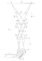
では、本発明の実施形態に係る照明装置、及び、投射型映像表示装置について図面を参照しつつ説明を行う。図1は、本発明の実施形態に係る照明装置を備えた投射型映像表示装置の構成を示す図である。なお、以下に説明する図面は、模式的に示した図であって、実際の形状、寸法、配置とは異なる場合もある。 Now, an illumination device and a projection display apparatus according to an embodiment of the present invention will be described with reference to the drawings. FIG. 1 is a diagram illustrating a configuration of a projection-type image display device including an illumination device according to an embodiment of the present invention. Note that the drawings described below are schematic views and may differ from actual shapes, dimensions, and arrangements.
本実施形態の投射型映像表示装置10は、照明装置20と、映像を形成するための光変調素子31、光変調素子31で形成された映像をスクリーン41に投射する投射光学系32などを備えている。なお、図では、映像が投影されるスクリーン41面をX−Y平面、それに直交する軸をZ軸としている。スクリーン41には、スクリーン41で反射された映像を観察する反射型スクリーン、あるいは、スクリーン41を透過した映像を観察する透過型スクリーンどちらを使用することもできる。
The projection-type
本実施形態の照明装置20は、光源11、光走査部15、光路変換系21を有して構成されている。なお、本発明でいう光学装置は、照明装置20から光源11を除いた光走査部15、光路変換系21から構成されるものである。
The illuminating
光源11は、コヒーレント光としてのレーザー光を出射する半導体レーザー装置など各種レーザー装置が使用される。光源11から出射されるコヒーレント光は、光走査部15を照明する。なお、光源11から出射されるコヒーレント光に対して、その断面方向の強度分布の均一化を図るビーム成型手段を設けておくことが好ましい。設計例として、光走査部近傍の面で均一化されるようにビーム成型手段を設けるとともに、その面と光変調素子面が共役になるよう光路変換系21を設定することにより、被照明領域を均一な強度で照明することが可能となる。またビーム成型手段は、強度を均一化すると同時に、レーザ
ビームの断面形状を光変調素子の形状に変形するものであってもよい。また、被照明領域としての光変調素子31の像形成領域の大きさ、光路変換系21の拡大率など各種条件によって、出射するコヒーレント光の口径をビームエキスパンダーにより調整することとしてもよい。
As the
光走査部15は、光源11にて出射されたコヒーレント光の方向を時間的に変化させる光学素子である。本実施形態では、回動中心Raを中心として反射面を回動させることのできるガルバノミラーが用いられている。この他、可動ミラーを機械的に回動させる可動式ミラーデバイスとしては、ポリゴンミラー、MEMSスキャナを用いることも考えられる。また、可動式ミラーデバイスに限らず、電気的に回折条件を変更することで、出射方向を変化させる可変回折型素子、あるいは、位相変調素子を用いることとしてもよい。このような素子では、可動式ミラーデバイスと異なり、可動部を有さないため、製造時あるいはメンテナンス時などの工程負担を軽減することが可能となる。詳細については後で説明する。
The
本実施形態の光走査部15は、Y軸方向に回動中心Raを有し、コヒーレント光をX−Z面内で走査する1次元的走査を行うこととしているが、光走査部15によるコヒーレント光の走査は1次元的、2次元的走査のどちらを利用してもよい。何れの場合においても光路変換系21の入射面を走査し、結果として被照明領域を十分に照明できることが必要とされる。
The
光源11から入射するコヒーレント光は、この光走査部15にて時間的に方向が変化する走査光Laとなり、光路変換系21に入射する。図では、最外端付近の走査光La(t1)とLa(t2)の様子が示されているが、実際には、走査光Laは、このLa(t1)とLa(t2)の間を経時的に連続移動もしくは間欠移動することとなる。
The coherent light incident from the
光路変換系21は、光走査部15から出射される走査光Laにて、被照明領域としての像形成領域を照明する光学素子である。光走査部15によって光走査された走査光Laは、この光路変換系21を経て、経時的に重なるように被照明領域を照明する。特に、本実施形態では、光路変換系21が被照明領域としての光変調素子31の像形成領域全体を、光走査部15の走査位置に関わらず常時照明することとしており、光の利用効率の向上が図られている。さらに、像形成領域を常時、平行光もしくは略平行光で照明することで、像形成領域の各点を同じ条件で照明しており、例えば、像形成領域全体を均一に照明することが可能となっている。
The optical
光変調素子31は、映像信号に基づいて像が形成される像形成領域を有するディスプレイであって、本実施形態では透過型の液晶表示素子が用いられている。光変調素子31としては、このような透過型のもの以外に、MEMSなどの反射型のものを利用することも可能である。光路変換系21からの照明光Lbは、時間の経過に伴い入射角度を変化させつつ光変調素子31に入射し、像形成領域に表示される像に基づいて変調光Lcに変換される。
The
投射光学系32は、光変調素子31からの変調光Lcを映像再生光Ldに拡大変換してスクリーン41に投射する。本実施形態では、この投射光学系32の後段に絞り33が設けられている。
The projection
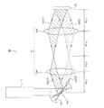
では、この投射型映像表示装置10において、スペックルを抑制するための主要構成である照明装置20について、その原理などを詳細に説明する。図2は、本発明の実施形態に係る照明装置20の構成を示す図であって、光路変換系21による照明の様子を示した図である。
Now, the principle and the like of the
図2に示されるように、時刻t1のときの走査光La(t1)は、光路変換系21に入射し、光変調素子31における像形成領域の少なくとも一部の領域を照明する照明光Lb(t1)に変換された後、当該領域を照明する。時刻t2のときの走査光La(t2)も同様に、光路変換系21にて照明光Lb(t2)に変換された後、像形成領域の少なくとも一部の領域を照明する。この図に示されるように照明装置20は、被照明領域に対する入射角度を時間的に変化させつつ像形成領域全体を照明することとなる。
As shown in FIG. 2, the scanning light La (t1) at time t1 enters the optical
本実施形態における光路変換系21は、第1集光素子21aと第2集光素子21bにて構成されている。図に示されるように第1集光素子21aは、前側焦点距離をF1_a、
後側焦点距離をF1_bとし、前側焦点位置に光走査部15の回動中心Raが位置してい
る。一方、第2集光素子21bは、前側焦点距離をF2_a、後側焦点距離をF2_bとし、後側焦点位置に光変調素子31の入射面が位置している。そして、第1集光素子21aの後側焦点位置は、第2集光素子21bの前側焦点位置に位置するように配置されている。
The optical
The rear focal length is F1_b, and the rotation center Ra of the
第1集光素子21aや第2集光素子21bとしては、集光機能を有する機能を有すればよく、レンズや凹面鏡などが用いられる。同等の機能を有するホログラム素子や回折素子などで実現してもよい。また、これらの組み合わせにより実現してもよい。また、光路変換系21は、走査されたコヒーレント光が被照明領域を経時的に重ねて照明するような機能を有すればよく、集光素子の組み合わせ以外にも、複数のミラーや複数のプリズム、複数の導光素子、光ファイバーアレイなどで実現してもよい。
As the
このような第1集光素子21a、第2集光素子21bの光学的配置にて、光源11から入射する平行あるいは略平行なコヒーレント光は、光変調素子31の所定領域全体を常時、平行あるいは略平行な照明光Lbで照明することが可能となる。本実施形態では、この照明光Lbが照明する所定領域が光変調素子31における像形成領域に設定されることとなる。像形成領域全体が常時照明されることで光の利用効率の向上を図られる。さらに、平行あるいは略平行な照明光Lbとすることで、像形成領域の各点を同じ条件で照明することが可能となる。
With such an optical arrangement of the
以上、光路変換系21について、第1集光素子21aと第2集光素子21bで構成されたものを説明したが、光路変換系21の構成は、この実施形態に限らず、走査光Laを被照明領域としての像形成領域の少なくとも一部分を照明すると共に、光走査部15による光走査に伴って、経時的に像形成領域全体を照明するものであればよい。
The optical
図1に戻り、光変調素子31で変調された変調光Lcは、投射光学系32で拡大され映像再生光Ldとしてスクリーン41上に投射され、反射、あるいは、透過される映像を観察者に観察させる。このときスクリーン41の面上で拡散されたコヒーレント光は互いに干渉することでスペックルを生じさせる。しかしながら、本実施形態では、光走査部15によってコヒーレント光が走査されるため、結果としてスクリーン41に投射する映像再生光Ldの入射角度を経時的に変化させ、このスペックルを極めて効果的に目立たなくしている。
Returning to FIG. 1, the modulated light Lc modulated by the
図1に示されるスクリーン上の点P1において、例えば、時刻t1における映像再生光Ld(t1)と、時刻t2における映像再生光Ld(t2)が異なる入射角度で照射されることとなる。図に示す他の点P2や図示しない他の点においても同様であって、映像再生光Ldは、入射角度を時間的に変化させつつスクリーン41上に映像を投射する。したがって、ごく短い時間ではスクリーン上に形成されるスペックルも、映像再生光Ldが時間によって異なる入射角度で照射されることで視覚の応答時間内で時間的に平均化され、
スクリーン41に投射される像を観察する観察者には十分に目立たない状態となる。
At the point P1 on the screen shown in FIG. 1, for example, the video reproduction light Ld (t1) at time t1 and the video reproduction light Ld (t2) at time t2 are irradiated at different incident angles. The same applies to other points P2 shown in the figure and other points not shown, and the image reproduction light Ld projects an image on the
It becomes a state which is not sufficiently conspicuous for an observer who observes an image projected on the
観察者によって観察されるスペックルには、このようにスクリーン41上でのコヒーレント光の散乱を原因として発生するスペックルだけではなく、投射型映像表示装置10の各種光学素子上で発生するものもある。このスペックルは、光変調素子31を介してスクリーン41に投影されることで観察者に観察される。本実施形態では、走査光Laが光路変換系21を走査することで、投射型映像表示装置10の各種光学素子で発生するスペックルを十分に目立たない状態とすることが可能となる。
The speckles observed by the observer are not only speckles generated due to the scattering of coherent light on the
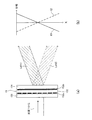
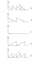
以上、図1、図2における本実施形態では光走査部15について、ガルバノミラーを用いた可動式ミラーデバイスについて説明したが、可動部を有さない可変回折型素子、あるいは、位相変調素子を使用することも可能である。図3は、本発明の他の実施形態に係る光走査部(可変回折型素子)の構成を示す図であり、図4は、本発明の他の実施形態に係る光走査部(位相変調素子)の構成と位相変化の様子を示す図であり、図5は、本発明の他の実施形態に係る光走査部(位相変調素子)における位相変化の様子を示す図である。
As described above, in the present embodiment in FIGS. 1 and 2, the movable mirror device using the galvano mirror has been described for the
図3の光走査部15は、可変回折型素子を利用した実施形態であって、この実施形態では、可変回折型素子として振幅変調型の液晶素子を利用したものとしている。光走査部15を構成する液晶素子は、液晶151によって回折格子を形成する。この液晶151によって形成される回折格子のピッチを時間的に変化させて回折角度を変えることで、光源11から入射されるコヒーレント光の出射方向を時間的に変化させることが可能となっている。本実施形態では、光走査部15の入射面に対して斜めにコヒーレント光を入射させることで、0次光を逃がすとともに、回折光を素子の法線方向に出射させることが可能となる。
The
可変回折型素子としては、この液晶素子以外に、音響光学素子など通過する光の位相を変調する光学素子を用いることとしてもよい。あるいは、反射させる光について位相を変調するマイクロミラーデバイスを用いることも可能である。 In addition to the liquid crystal element, an optical element that modulates the phase of light passing therethrough may be used as the variable diffraction element. Alternatively, a micromirror device that modulates the phase of the reflected light can be used.
図4の光走査部15は、位相変調素子を利用した実施形態であって、この実施形態では、位相のみの変調を行う液晶素子を利用したものとしている。図4(a)は、この構成例を示した図であって、光走査部15は、透明基材153、154の間に封入された液晶層152を有して構成されている。液晶層152には、部分毎に配設された画素電極152aと、共通電極152bが設けられており、部分毎に経時的に屈折率を変化させることで透過光の位相を変化させることが可能となっている。
The
図4(b)は、位相変化の基本型を示した図であって、図4(a)の構成図と対応した形で位相分布が示されている。画素電極152aに印加するバイアスを時間的に変化させることで、例えば、時刻t1、t2に示すような位相分布を形成することが可能である。このような位相分布では、図4(a)に示すように時刻t1では、走査光La(t1)が、時刻t2では、走査光La(t2)の状態に偏向させることが可能となる。実際には、t1の位相状態とt2の位相状間を多段階あるいは連続的に変化させることで、走査光Laについても多段階あるいは連続的に方向を変化させることが可能となる。
FIG. 4B is a diagram showing a basic type of phase change, and the phase distribution is shown in a form corresponding to the configuration diagram of FIG. By changing the bias applied to the
図5は、位相変化の他の形態を示した図であって、位相分布をキノフォーム型に、すなわち0〜2πで繰り返すパターンを時間的に変更することで、偏向条件を経時的に変更し、図4(b)の場合と同様に偏向方向を変化させるものである。この図は、図4(b)と同様、図4(a)の構成図と対応した形で位相分布が示されたものであって、図5(a)は、時刻t1における位相状態、図5(e)は、時刻t2における位相状態が示されている。図5(a)から図5(e)、図5(e)から図5(a)間の位相形状を時間的に変化
させることで、光源11から入射されるコヒーレント光を偏向させている。なお、位相分布は、0〜2π以外の範囲に設定されたフレネルレンズ型を用いることとしてもよい。
FIG. 5 is a diagram showing another form of phase change, in which the deflection condition is changed over time by changing the phase distribution into a kinoform type, that is, by changing a pattern that repeats from 0 to 2π over time. As in the case of FIG. 4B, the deflection direction is changed. This figure shows the phase distribution corresponding to the configuration diagram of FIG. 4A, as in FIG. 4B, and FIG. 5A shows the phase state at time t1, and FIG. 5 (e) shows the phase state at time t2. Coherent light incident from the
このように光走査部15に位相変調素子を利用した場合には、前述の可変回折型素子を利用した場合と異なり0次光が発生しないため、光の利用効率の向上が図られる。また、図に示すように光走査部15の入射面に対して垂直にコヒーレント光を入射させることも可能となる。
As described above, when the phase modulation element is used in the
以上、本実施形態によれば、スペックルノイズが目立たない照明装置、並びに、この照明装置にて光変調素子31を照明することでスペックルノイズが目立たない映像を提供することのできる投射型映像表示装置を提供することが可能となる。特に、本実施形態では、光走査部15にて走査された光を、光路変換系21を介して照明することで光の利用効率向上が図られる。
As described above, according to the present embodiment, an illumination device in which speckle noise is not noticeable, and a projection-type image that can provide an image in which speckle noise is not noticeable by illuminating the
なお、本発明はこれらの実施形態のみに限られるものではなく、それぞれの実施形態の構成を適宜組み合わせて構成した実施形態も本発明の範疇となるものである。 Note that the present invention is not limited to these embodiments, and embodiments configured by appropriately combining the configurations of the respective embodiments also fall within the scope of the present invention.
10…投射型映像表示装置
11…光源
15…光走査部
151…液晶
152…液晶層
152a…画素電極
152b…共通電極
153、154…透明基材
21…光路変換系
21a…第1集光素子
21b…第2集光素子
DESCRIPTION OF
Claims (10)
前記光源から出射されたコヒーレント光を走査する光走査部と、
前記光走査部にて走査されたコヒーレント光が被照明領域を経時的に重ねて照明するように設定された光路変換系と、を備え、
前記被照明領域の各点に入射するコヒーレント光の入射角度は、時間とともに変化することを特徴とする
照明装置。 A light source that emits coherent light;
An optical scanning unit that scans coherent light emitted from the light source;
An optical path conversion system set so that the coherent light scanned by the optical scanning unit illuminates the illuminated region over time, and
An illumination apparatus, wherein an incident angle of coherent light incident on each point of the illuminated region changes with time.
請求項1に記載の照明装置。 The illumination apparatus according to claim 1, wherein the optical path conversion system illuminates the entire illuminated area regardless of a scanning position of coherent light in the optical scanning unit.
前記光走査部は、前記第1集光素子の前側焦点位置に設けられ、
前記第1集光素子の後側焦点位置に前記第2集光素子の前側焦点位置が設けられ、
前記第2集光素子の後側焦点位置に被照明領域が位置することを特徴とする
請求項1または請求項2に記載の照明装置。 The optical path conversion system includes a first light collecting element and a second light collecting element,
The optical scanning unit is provided at a front focal position of the first light collecting element,
A front focal position of the second light collecting element is provided at a rear focal position of the first light collecting element;
The illumination device according to claim 1, wherein an illuminated region is located at a rear focal position of the second light collecting element.
請求項1から請求項3の何れか1項に記載の照明装置。 The illumination device according to any one of claims 1 to 3, wherein the optical scanning unit includes a galvanometer mirror.
請求項1から請求項3の何れか1項に記載の照明装置。 The illumination device according to any one of claims 1 to 3, wherein the optical scanning unit includes a polygon mirror.
請求項1から請求項3の何れか1項に記載の照明装置。 The illumination device according to any one of claims 1 to 3, wherein the optical scanning unit includes a variable diffraction element.
請求項1から請求項3の何れか1項に記載の照明装置。 The illumination device according to any one of claims 1 to 3, wherein the light scanning unit includes a phase modulation element.
請求項1から請求項7の何れか1項に記載の照明装置。 The illumination device according to any one of claims 1 to 7, wherein a beam shaping unit is disposed between the light source and the optical scanning unit.
前記光源から出射されたコヒーレント光を走査する光走査部と、
像が形成される像形成領域を有する光変調素子と、
前記光走査部にて走査されたコヒーレント光が前記像形成領域を経時的に重ねて照明するように設定された光路変換系と、
前記光変調素子の像をスクリーンに投影する投射光学系と、を備え
前記像形成領域の各点に入射するコヒーレント光の入射角度は、時間とともに変化することを特徴とする
投射型映像表示装置。 A light source that emits coherent light;
An optical scanning unit that scans coherent light emitted from the light source;
A light modulation element having an image forming region on which an image is formed;
An optical path conversion system set so that coherent light scanned by the optical scanning unit illuminates the image forming region over time;
A projection optical system that projects an image of the light modulation element onto a screen; and an incident angle of coherent light incident on each point of the image forming region changes with time.
前記光走査部にて走査されたコヒーレント光が被照明領域を経時的に重ねて照明するように設定された光路変換系と、を備えることを特徴とする
光学装置。 An optical scanning unit that scans coherent light;
An optical device comprising: an optical path changing system set so that the coherent light scanned by the optical scanning unit illuminates the illuminated region over time.
Priority Applications (9)
| Application Number | Priority Date | Filing Date | Title |
|---|---|---|---|
| JP2011105457A JP5541462B2 (en) | 2011-05-10 | 2011-05-10 | Projection-type image display device |
| US14/115,732 US9052524B2 (en) | 2011-05-10 | 2012-04-23 | Illumination device, projection type image display device, and optical device |
| PCT/JP2012/060876 WO2012153627A1 (en) | 2011-05-10 | 2012-04-23 | Illumination device, projection-type image display device, and optical device |
| EP12782392.0A EP2708949B1 (en) | 2011-05-10 | 2012-04-23 | Illumination device, projection-type image display device, and optical device |
| CN201280022254.2A CN103797414B (en) | 2011-05-10 | 2012-04-23 | Lighting device, projection type video display apparatus and optical devices |
| EP16181373.8A EP3118679B1 (en) | 2011-05-10 | 2012-04-23 | Illumination device |
| CN201510587932.5A CN105137594B (en) | 2011-05-10 | 2012-04-23 | Lighting device |
| US14/691,429 US9360679B2 (en) | 2011-05-10 | 2015-04-20 | Illumination device, projection type image display device, and optical device |
| US15/149,831 US9772504B2 (en) | 2011-05-10 | 2016-05-09 | Illumination device, projection type image display device, and optical device |
Applications Claiming Priority (1)
| Application Number | Priority Date | Filing Date | Title |
|---|---|---|---|
| JP2011105457A JP5541462B2 (en) | 2011-05-10 | 2011-05-10 | Projection-type image display device |
Related Child Applications (1)
| Application Number | Title | Priority Date | Filing Date |
|---|---|---|---|
| JP2014097264A Division JP5794442B2 (en) | 2014-05-09 | 2014-05-09 | Projection-type image display device |
Publications (3)
| Publication Number | Publication Date |
|---|---|
| JP2012237814A true JP2012237814A (en) | 2012-12-06 |
| JP2012237814A5 JP2012237814A5 (en) | 2014-04-10 |
| JP5541462B2 JP5541462B2 (en) | 2014-07-09 |
Family
ID=47139113
Family Applications (1)
| Application Number | Title | Priority Date | Filing Date |
|---|---|---|---|
| JP2011105457A Active JP5541462B2 (en) | 2011-05-10 | 2011-05-10 | Projection-type image display device |
Country Status (5)
| Country | Link |
|---|---|
| US (3) | US9052524B2 (en) |
| EP (2) | EP3118679B1 (en) |
| JP (1) | JP5541462B2 (en) |
| CN (2) | CN105137594B (en) |
| WO (1) | WO2012153627A1 (en) |
Cited By (7)
| Publication number | Priority date | Publication date | Assignee | Title |
|---|---|---|---|---|
| WO2015049866A1 (en) * | 2013-10-02 | 2015-04-09 | 日本電気株式会社 | Interface apparatus, module, control component, control method, and program storage medium |
| WO2015147185A1 (en) * | 2014-03-27 | 2015-10-01 | 大日本印刷株式会社 | Lighting apparatus |
| US9354503B2 (en) | 2013-05-23 | 2016-05-31 | Seiko Epson Corporation | Laser projector |
| JP2017505555A (en) * | 2013-10-20 | 2017-02-16 | エムティティ イノベーション インコーポレイテッドMtt Innovation Incorporated | Light field projector and method |
| WO2018179980A1 (en) * | 2017-03-31 | 2018-10-04 | 日本電気株式会社 | Projection device, projection image control method, and recording medium having projection image control program recorded thereon |
| JP2019091652A (en) * | 2017-11-16 | 2019-06-13 | スタンレー電気株式会社 | Light irradiation device and vehicular lamp |
| US11363242B2 (en) | 2014-05-15 | 2022-06-14 | Mtt Innovation Incorporated | Optimizing drive schemes for multiple projector systems |
Families Citing this family (11)
| Publication number | Priority date | Publication date | Assignee | Title |
|---|---|---|---|---|
| CN107107807B (en) * | 2014-11-07 | 2021-03-19 | 大日本印刷株式会社 | Lighting device |
| US10627053B2 (en) * | 2015-06-22 | 2020-04-21 | Dai Dippon Printing Co., Ltd. | Illumination device including coherent light source to illuminate an illumination area |
| US10941915B2 (en) * | 2015-09-07 | 2021-03-09 | Dai Nippon Printing Co., Ltd. | Illumination device for illuminating a predetermined range with coherent light |
| US10732414B2 (en) * | 2016-08-17 | 2020-08-04 | Microsoft Technology Licensing, Llc | Scanning in optical systems |
| CN106195929A (en) * | 2016-09-03 | 2016-12-07 | 超视界激光科技(苏州)有限公司 | Laser light source module |
| US20200041880A1 (en) * | 2016-10-20 | 2020-02-06 | Dai Nippon Printing Co., Ltd. | Display device |
| US10553139B2 (en) | 2016-11-10 | 2020-02-04 | Microsoft Technology Licensing, Llc | Enhanced imaging system for linear micro-displays |
| JP7217231B2 (en) * | 2017-07-04 | 2023-02-02 | マクセル株式会社 | Projection optical system and head-up display device |
| CN109425995A (en) * | 2017-08-24 | 2019-03-05 | 陈致晓 | Laser illumination system and its laser facula removing method |
| CN109946918B (en) * | 2019-04-26 | 2021-04-20 | 四川省派瑞克斯光电科技有限公司 | 3D projection angle control method, device and system |
| US11940139B2 (en) * | 2019-06-28 | 2024-03-26 | Dai Nippon Printing Co., Ltd. | Lighting device and lighting method |
Citations (4)
| Publication number | Priority date | Publication date | Assignee | Title |
|---|---|---|---|---|
| JPS61212816A (en) * | 1985-03-18 | 1986-09-20 | Canon Inc | Lighting equipment |
| JP2004191839A (en) * | 2002-12-13 | 2004-07-08 | Seiko Epson Corp | Projector |
| JP2008256824A (en) * | 2007-04-03 | 2008-10-23 | Seiko Epson Corp | Light source device and projector |
| JP2009163901A (en) * | 2007-12-28 | 2009-07-23 | Seiko Epson Corp | Light source device, and projector |
Family Cites Families (15)
| Publication number | Priority date | Publication date | Assignee | Title |
|---|---|---|---|---|
| US5313479A (en) | 1992-07-29 | 1994-05-17 | Texas Instruments Incorporated | Speckle-free display system using coherent light |
| US5845981A (en) * | 1997-12-29 | 1998-12-08 | Philips Electronics North America Corporation | Multi-color-band scrolling across single-panel light valve |
| US6183092B1 (en) * | 1998-05-01 | 2001-02-06 | Diane Troyer | Laser projection apparatus with liquid-crystal light valves and scanning reading beam |
| US6597090B1 (en) * | 1998-09-28 | 2003-07-22 | Xidex Corporation | Method for manufacturing carbon nanotubes as functional elements of MEMS devices |
| US6540362B1 (en) * | 2000-08-09 | 2003-04-01 | Koninklijke Philips Electronics N.V. | Scrolling multi-stripe color illumination system |
| JP2003015217A (en) * | 2001-07-02 | 2003-01-15 | Matsushita Electric Ind Co Ltd | Projection type image display device |
| US6577429B1 (en) * | 2002-01-15 | 2003-06-10 | Eastman Kodak Company | Laser projection display system |
| US7088353B2 (en) * | 2002-07-10 | 2006-08-08 | Fuji Photo Film Co., Ltd. | Display device |
| WO2006137326A1 (en) | 2005-06-20 | 2006-12-28 | Matsushita Electric Industrial Co., Ltd. | 2-dimensional image display device, illumination light source, and exposure illumination device |
| JP2007179314A (en) | 2005-12-28 | 2007-07-12 | Star Micronics Co Ltd | Machine tool and program conversion method therefor |
| EP1976303A1 (en) * | 2007-03-31 | 2008-10-01 | Sony Deutschland Gmbh | Image generating apparatus |
| WO2009010978A1 (en) * | 2007-07-17 | 2009-01-22 | Explay Ltd. | Coherent imaging method of laser projection and apparatus thereof |
| JP5737633B2 (en) * | 2010-09-08 | 2015-06-17 | 大日本印刷株式会社 | Illumination device, projection device, and projection-type image display device |
| JP5804243B2 (en) * | 2011-04-22 | 2015-11-04 | 大日本印刷株式会社 | Projection-type image display device |
| JP5168526B2 (en) * | 2011-05-10 | 2013-03-21 | 大日本印刷株式会社 | Projection-type image display device |
-
2011
- 2011-05-10 JP JP2011105457A patent/JP5541462B2/en active Active
-
2012
- 2012-04-23 CN CN201510587932.5A patent/CN105137594B/en active Active
- 2012-04-23 EP EP16181373.8A patent/EP3118679B1/en active Active
- 2012-04-23 WO PCT/JP2012/060876 patent/WO2012153627A1/en active Application Filing
- 2012-04-23 EP EP12782392.0A patent/EP2708949B1/en not_active Not-in-force
- 2012-04-23 CN CN201280022254.2A patent/CN103797414B/en not_active Expired - Fee Related
- 2012-04-23 US US14/115,732 patent/US9052524B2/en active Active
-
2015
- 2015-04-20 US US14/691,429 patent/US9360679B2/en active Active
-
2016
- 2016-05-09 US US15/149,831 patent/US9772504B2/en active Active
Patent Citations (4)
| Publication number | Priority date | Publication date | Assignee | Title |
|---|---|---|---|---|
| JPS61212816A (en) * | 1985-03-18 | 1986-09-20 | Canon Inc | Lighting equipment |
| JP2004191839A (en) * | 2002-12-13 | 2004-07-08 | Seiko Epson Corp | Projector |
| JP2008256824A (en) * | 2007-04-03 | 2008-10-23 | Seiko Epson Corp | Light source device and projector |
| JP2009163901A (en) * | 2007-12-28 | 2009-07-23 | Seiko Epson Corp | Light source device, and projector |
Cited By (13)
| Publication number | Priority date | Publication date | Assignee | Title |
|---|---|---|---|---|
| US9354503B2 (en) | 2013-05-23 | 2016-05-31 | Seiko Epson Corporation | Laser projector |
| JPWO2015049866A1 (en) * | 2013-10-02 | 2017-03-09 | 日本電気株式会社 | Interface device, module, control component, control method, and computer program |
| WO2015049866A1 (en) * | 2013-10-02 | 2015-04-09 | 日本電気株式会社 | Interface apparatus, module, control component, control method, and program storage medium |
| JP2017505555A (en) * | 2013-10-20 | 2017-02-16 | エムティティ イノベーション インコーポレイテッドMtt Innovation Incorporated | Light field projector and method |
| WO2015147185A1 (en) * | 2014-03-27 | 2015-10-01 | 大日本印刷株式会社 | Lighting apparatus |
| JP2015191043A (en) * | 2014-03-27 | 2015-11-02 | 大日本印刷株式会社 | Lighting device |
| US10175497B2 (en) | 2014-03-27 | 2019-01-08 | Dai Nippon Printing Co., Ltd. | Illumination device and projector |
| US11363242B2 (en) | 2014-05-15 | 2022-06-14 | Mtt Innovation Incorporated | Optimizing drive schemes for multiple projector systems |
| WO2018179980A1 (en) * | 2017-03-31 | 2018-10-04 | 日本電気株式会社 | Projection device, projection image control method, and recording medium having projection image control program recorded thereon |
| JPWO2018179980A1 (en) * | 2017-03-31 | 2019-11-21 | 日本電気株式会社 | Projection device, projection image control method, and recording medium on which projection image control program is recorded |
| US10859845B2 (en) | 2017-03-31 | 2020-12-08 | Nec Corporation | Projection device, projection image control method, and recording medium having projection image control program recorded thereon |
| JP7053227B2 (en) | 2017-11-16 | 2022-04-12 | スタンレー電気株式会社 | Light irradiation device and vehicle lighting equipment |
| JP2019091652A (en) * | 2017-11-16 | 2019-06-13 | スタンレー電気株式会社 | Light irradiation device and vehicular lamp |
Also Published As
| Publication number | Publication date |
|---|---|
| CN103797414B (en) | 2015-10-07 |
| CN105137594B (en) | 2018-02-16 |
| US20160252744A1 (en) | 2016-09-01 |
| US20150036108A1 (en) | 2015-02-05 |
| US20150226977A1 (en) | 2015-08-13 |
| US9360679B2 (en) | 2016-06-07 |
| CN105137594A (en) | 2015-12-09 |
| JP5541462B2 (en) | 2014-07-09 |
| EP3118679B1 (en) | 2020-04-15 |
| US9052524B2 (en) | 2015-06-09 |
| EP2708949A4 (en) | 2015-04-15 |
| WO2012153627A1 (en) | 2012-11-15 |
| EP2708949B1 (en) | 2016-08-17 |
| EP3118679A1 (en) | 2017-01-18 |
| CN103797414A (en) | 2014-05-14 |
| EP2708949A1 (en) | 2014-03-19 |
| US9772504B2 (en) | 2017-09-26 |
Similar Documents
| Publication | Publication Date | Title |
|---|---|---|
| JP5541462B2 (en) | Projection-type image display device | |
| JP5168526B2 (en) | Projection-type image display device | |
| JP6304337B2 (en) | Illumination device, projection device, and projection-type image display device | |
| JP6226252B2 (en) | Illumination device, projection device, and projection-type image display device | |
| JP2012237811A (en) | Illumination device, projection video display device, and light deflecting device | |
| JP5207013B2 (en) | Illumination device and optical device | |
| JP5804245B2 (en) | Scanning display device | |
| JP6308355B2 (en) | LIGHTING DEVICE, PROJECTION VIDEO DISPLAY DEVICE, OPTICAL DEVICE, AND OPTICAL ELEMENT | |
| JP5794442B2 (en) | Projection-type image display device | |
| JP6460182B2 (en) | Illumination device and light deflection device | |
| JP2012237812A (en) | Illumination device, projection video display device, and light deflecting device | |
| JP5812390B2 (en) | Illumination device, projection device, and projection-type image display device | |
| JP6198151B2 (en) | Illumination device and light deflection device |
Legal Events
| Date | Code | Title | Description |
|---|---|---|---|
| A521 | Written amendment |
Free format text: JAPANESE INTERMEDIATE CODE: A523 Effective date: 20140220 |
|
| A621 | Written request for application examination |
Free format text: JAPANESE INTERMEDIATE CODE: A621 Effective date: 20140220 |
|
| A871 | Explanation of circumstances concerning accelerated examination |
Free format text: JAPANESE INTERMEDIATE CODE: A871 Effective date: 20140220 |
|
| A975 | Report on accelerated examination |
Free format text: JAPANESE INTERMEDIATE CODE: A971005 Effective date: 20140311 |
|
| TRDD | Decision of grant or rejection written | ||
| A01 | Written decision to grant a patent or to grant a registration (utility model) |
Free format text: JAPANESE INTERMEDIATE CODE: A01 Effective date: 20140409 |
|
| A61 | First payment of annual fees (during grant procedure) |
Free format text: JAPANESE INTERMEDIATE CODE: A61 Effective date: 20140422 |
|
| R150 | Certificate of patent or registration of utility model |
Ref document number: 5541462 Country of ref document: JP Free format text: JAPANESE INTERMEDIATE CODE: R150 |