JP2012209826A - Multiple frequency band passing filter - Google Patents
Multiple frequency band passing filter Download PDFInfo
- Publication number
- JP2012209826A JP2012209826A JP2011074926A JP2011074926A JP2012209826A JP 2012209826 A JP2012209826 A JP 2012209826A JP 2011074926 A JP2011074926 A JP 2011074926A JP 2011074926 A JP2011074926 A JP 2011074926A JP 2012209826 A JP2012209826 A JP 2012209826A
- Authority
- JP
- Japan
- Prior art keywords
- bandpass filter
- dielectric block
- filter unit
- conductor
- frequency
- Prior art date
- Legal status (The legal status is an assumption and is not a legal conclusion. Google has not performed a legal analysis and makes no representation as to the accuracy of the status listed.)
- Pending
Links
Images


Abstract
Description
本発明は、誘電体ブロックに複数の共振器を形成してなる、マイクロ波帯域などの高周波帯域で使用する帯域フィルタに関する。さらに詳しくは、本発明は、一組の入出力端子間に挿入され、複数の周波数帯域を通過させる複数周波数帯域通過フィルタに関する。 The present invention relates to a bandpass filter used in a high frequency band such as a microwave band, in which a plurality of resonators are formed in a dielectric block. More specifically, the present invention relates to a multi-frequency bandpass filter that is inserted between a set of input / output terminals and passes a plurality of frequency bands.
本発明の複数周波数帯域通過フィルタは、たとえば、携帯電話機の2周波数帯域用アンテナに接続される2周波数帯域通過フィルタとして好適である。 The multi-frequency bandpass filter of the present invention is suitable as a two-frequency bandpass filter connected to a two-frequency band antenna of a mobile phone, for example.
従来、携帯電話機などの移動体通信機器は、アンテナにより送受信する信号を帯域通過フィルタなどのフィルタを介して、所望の周波数帯域のみを送受信することができるように構成されている。 2. Description of the Related Art Conventionally, mobile communication devices such as mobile phones are configured so that signals transmitted and received by an antenna can be transmitted and received only in a desired frequency band through a filter such as a band pass filter.
近年、複数の通信システムに対応することの可能な携帯電話機が提案されている。そのような携帯電話機では、1個のアンテナにより複数の高周波数帯域を送受信することができるようにし、フィルタを用いて、必要に応じて所望の周波数帯域を選んで使用するようになっている。 In recent years, mobile phones capable of supporting a plurality of communication systems have been proposed. In such a mobile phone, a plurality of high frequency bands can be transmitted and received by one antenna, and a desired frequency band is selected and used as necessary using a filter.
複数周波数帯域用のフィルタに関しては、次のような技術的背景がある。すなわち、近年、電子機器の発展に伴い増幅器の特性が非常に広帯域化しており、たとえば2つの周波数帯域を同じ増幅器で増幅することができる。そこで、そのような増幅器を使用する通信機器においては、互いに異なる周波数帯域で使用される同種部品の共通化を図ることができれば、通信機器を構成する部品点数が少なくなると同時に、通信機器の小型化が図れるので好ましい。 Regarding filters for multiple frequency bands, there is the following technical background. That is, in recent years, with the development of electronic equipment, the characteristics of amplifiers have become very wide, and for example, two frequency bands can be amplified with the same amplifier. Therefore, in communication equipment using such an amplifier, if the same kind of parts used in different frequency bands can be shared, the number of parts constituting the communication equipment can be reduced, and at the same time, the size of the communication equipment can be reduced. Is preferable.
2つの周波数帯域システムに適合して、互いに異なる周波数帯域を独立に信号処理するためには、所望の周波数帯域外の周波数域を良好に減衰させることが必要である。2周波数帯域をそれぞれ分離して信号処理することを可能にする帯域通過フィルタとして、特許文献1に記載されるような構造が提案されている。 In order to adapt to two frequency band systems and independently perform signal processing on different frequency bands, it is necessary to satisfactorily attenuate frequency bands outside the desired frequency band. A structure as described in Patent Document 1 has been proposed as a band-pass filter that enables signal processing by separating two frequency bands.
また、2周波数帯域をそれぞれ分離して信号処理することを可能にする別の帯域通過フィルタとして、特許文献2に記載されるような構造が提案されている。
A structure as described in
しかしながら、特許文献1に記載される技術であって導波管或いは空洞共振器を用いる方法は、構造が複雑で大型になるため、近年の携帯電話機などの移動体通信機器における小型化の要求を満たすことができない。一方、特許文献1に記載される技術であってマイクロストリップ線路を用いる方法は、双方のフィルタが互いに結合してしまい良好な減衰を得ることができない。 However, the technique described in Patent Document 1 that uses a waveguide or a cavity resonator has a complicated structure and becomes large in size, and thus there has been a demand for downsizing in mobile communication devices such as mobile phones in recent years. I can't meet. On the other hand, in the technique described in Patent Document 1 and using a microstrip line, both filters are coupled to each other, and good attenuation cannot be obtained.
また、特許文献2に記載される技術であって構造を小型化するために内導体と外導体との間に誘電体を充填する方法では、2つの帯域通過部を仕切るための仕切り板を配置するので、部品点数が多くなる。また、特許文献2に記載される帯域通過フィルタを製造する際には、内導体と外導体との間にセラミックや有機材料を充填して固化したり、複数のセラミックグリーンシートをプレス加工した後に焼結する等の複雑な工程が必要であり、製造が複雑でコスト増となる。すなわち、特許文献2に記載される技術では、安価で低損失の誘電体ブロックを使用することができない。
Further, in the technique described in
本発明は、上記事情に鑑みてなされたものであり、小型で、減衰特性が良好で、製造が容易な複数周波帯域通過フィルタを提供することを目的とする。 The present invention has been made in view of the above circumstances, and an object of the present invention is to provide a multi-frequency bandpass filter that is small in size, good in attenuation characteristics, and easy to manufacture.
本発明によれば、以上の如き目的を達成するものとして、
互いに略平行な第1の面及び第2の面と、前記第1の面及び第2の面と略直交し且つ互いに略平行な第3の面及び第4の面と、を含む外面、を有する誘電体ブロックと、
該誘電体ブロックを用いて構成される第1帯域通過フィルタ部及び第2帯域通過フィルタ部と、
を含んでなる複数周波数帯域通過フィルタであって、
前記第1帯域通過フィルタ部は、
前記誘電体ブロックに前記第1の面から前記第2の面にかけて形成され、前記第3の面に沿って配列された複数の第1の貫通孔からなる第1貫通孔群と、
前記第1の貫通孔の内面に形成された第1内導体と、
前記第1の面を除く前記誘電体ブロックの外面に形成された外導体と、
前記第1の面にて前記第1内導体から延び、前記第1の貫通孔に対応して形成される共振器同士を結合させる第1結合電極と、
を含んでなり、
前記第2帯域通過フィルタ部は、
前記誘電体ブロックに前記第1の面から前記第2の面にかけて形成され、前記第4の面に沿って配列された複数の第2の貫通孔からなる第2貫通孔群と、
前記第2の貫通孔の内面に形成された第2内導体と、
前記第1の面を除く前記誘電体ブロックの外面に形成された外導体と、
前記第1の面にて前記第2内導体から延び、前記第2の貫通孔に対応して形成される共振器同士を結合させる第2結合電極と、
を含んでなり、
前記第1の面には、前記第1帯域通過フィルタ部の一方端部の共振器及び前記第2帯域通過フィルタ部の一方端部の共振器と結合する第1共通電極と、前記第1帯域通過フィルタ部の他方端部の共振器及び前記第2帯域通過フィルタ部の他方端部の共振器と結合する第2共通電極と、が形成されており、
前記誘電体ブロックには、前記第1貫通孔群と前記第2貫通孔群との間に介在し、前記第1の面から前記第2の面にかけて形成され、前記第3の面及び前記第4の面と略平行に延びたスリットが形成されており、
該スリットの内面には、前記第2の面に形成された前記外導体と接続されたシールド導体が形成されている、
ことを特徴とする、複数周波数帯域通過フィルタ、
が提供される。
According to the present invention, the object as described above is achieved.
A first surface and a second surface that are substantially parallel to each other; and an outer surface that includes a third surface and a fourth surface that are substantially orthogonal to the first surface and the second surface and substantially parallel to each other. Having a dielectric block;
A first bandpass filter unit and a second bandpass filter unit configured using the dielectric block;
A multi-frequency bandpass filter comprising
The first band pass filter unit is:
A first through hole group comprising a plurality of first through holes formed in the dielectric block from the first surface to the second surface and arranged along the third surface;
A first inner conductor formed on the inner surface of the first through hole;
An outer conductor formed on an outer surface of the dielectric block excluding the first surface;
A first coupling electrode extending from the first inner conductor on the first surface and coupling resonators formed corresponding to the first through holes;
Comprising
The second bandpass filter unit is
A second through hole group comprising a plurality of second through holes formed in the dielectric block from the first surface to the second surface and arranged along the fourth surface;
A second inner conductor formed on the inner surface of the second through hole;
An outer conductor formed on an outer surface of the dielectric block excluding the first surface;
A second coupling electrode extending from the second inner conductor on the first surface and coupling resonators formed corresponding to the second through holes;
Comprising
The first surface includes a first common electrode coupled to a resonator at one end of the first bandpass filter unit and a resonator at one end of the second bandpass filter unit, and the first band. A resonator at the other end of the pass filter section and a second common electrode coupled to the resonator at the other end of the second band pass filter section are formed,
The dielectric block is interposed between the first through-hole group and the second through-hole group and is formed from the first surface to the second surface, and the third surface and the second surface A slit extending substantially parallel to the surface of 4 is formed,
On the inner surface of the slit, a shield conductor connected to the outer conductor formed on the second surface is formed.
A multi-frequency bandpass filter, characterized by
Is provided.
本発明の一態様においては、前記誘電体ブロックは、前記第1の面及び前記第2の面と略平行な断面の形状が前記第1の面から前記第2の面に至るまで同一である。本発明の一態様においては、前記誘電体ブロックは誘電体セラミックからなる。本発明の一態様においては、前記第1の面を略覆うように配置された電磁シールドカバーを備えている。 In one aspect of the present invention, the dielectric block has the same cross-sectional shape substantially parallel to the first surface and the second surface from the first surface to the second surface. . In one aspect of the present invention, the dielectric block is made of a dielectric ceramic. In one aspect of the present invention, an electromagnetic shield cover is provided so as to substantially cover the first surface.
本発明によれば、小型で、減衰特性が良好で、製造が容易な複数周波帯域通過フィルタが提供される。 According to the present invention, there is provided a multi-frequency bandpass filter that is small, has good attenuation characteristics, and is easy to manufacture.
以下、図面を参照しながら本発明の具体的な実施形態を説明する。 Hereinafter, specific embodiments of the present invention will be described with reference to the drawings.
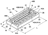
図1は、本発明による複数周波数帯域通過フィルタの第1の実施形態を示す模式的斜視図である。図2は、本実施形態の複数周波数帯域通過フィルタの模式的断面図である。本実施形態においては、複数周波数帯域通過フィルタは2周波数帯域通過フィルタである。 FIG. 1 is a schematic perspective view showing a first embodiment of a multi-frequency bandpass filter according to the present invention. FIG. 2 is a schematic cross-sectional view of the multi-frequency bandpass filter of the present embodiment. In the present embodiment, the multiple frequency bandpass filter is a two-frequency bandpass filter.
本実施形態の2周波数帯域通過フィルタは、誘電体ブロック2を有する。誘電体ブロック2の材質としては、たとえば誘電体セラミックを使用することができ、特に比誘電率εrが10程度のフォルステライト系セラミックを使用することができる。
The two-frequency bandpass filter of this embodiment has a
誘電体ブロック2は、互いに略平行な第1の面21及び第2の面22を有する。誘電体ブロック2は、更に、第1の面21及び第2の面22と略直交し且つ互いに略平行な第3の面23及び第4の面24を有する。誘電体ブロック2は、更に、第1の面21及び第2の面22並びに第3の面23及び第4の面24と略直交し且つ互いに略平行な第5の面25及び第6の面26を有する。かくして、誘電体ブロック2の外面は、第1の面21〜第6の面26を含んでなる。
The
第1の面21は上面である。第2の面22は、下面であり、第1の面21から距離(高さ)Hを隔てて第1の面21と反対向き且つ略平行に位置している。第3の面23及び第4の面24は、一対の側面であり、距離(幅)Wを隔てて互いに反対向きに位置している。第5の面25及び第6の面26は、一対の端面であり、距離(長さ)Lを隔てて互いに反対向きに位置している。誘電体ブロック2の寸法は、所要の特性に応じて、適宜設定することができるが、例えば、Hは4mm〜25mm、Lは60mm〜130mm、Wは25mm〜60mmである。また、Lは3W以内が好ましい。一例を挙げれば、長さLが約70mmで、幅Wが約35mmで、高さHが約9mmである。
The
2周波数帯域通過フィルタは、誘電体ブロック2を用いて構成される第1帯域通過フィルタ部4A及び第2帯域通過フィルタ部4Bを含む。
The two-frequency bandpass filter includes a first
第1帯域通過フィルタ部4Aは、誘電体ブロック2に第1の面21から第2の面22にかけて形成され、第3の面23に沿って配列された複数の第1の貫通孔41Aからなる第1貫通孔群40Aと、第1の貫通孔41Aの内面に形成された第1内導体42Aと、第1の面21を除く誘電体ブロック2の外面に形成された外導体43と、第1の面21にて第1内導体42Aから延び、第1の貫通孔41Aに対応して形成される1/4波長型の共振器同士を結合させる第1結合電極44Aと、を含んでなる。
The first band
同様に、第2帯域通過フィルタ部4Bは、誘電体ブロック2に第1の面21から第2の面22にかけて形成され、第4の面24に沿って配列された複数の第2の貫通孔41Bからなる第2貫通孔群40Bと、第2の貫通孔41Bの内面に形成された第2内導体42Bと、第1の面21を除く誘電体ブロック2の外面に形成された外導体43と、第1の面21にて第2内導体42Bから延び、第2の貫通孔41Bに対応して形成される1/4波長型の共振器同士を結合させる第2結合電極44Bと、を含んでなる。
Similarly, the second band-
誘電体ブロック2には、第1貫通孔群40Aと第2貫通孔群40Bとの間に介在し、第1の面21から第2の面22にかけて形成されたスリット8が形成されている。スリット8は、第3の面23及び第4の面24と略平行に延びており、全体として幅Dを持つ貫通長孔形状をなしている。幅Dは、適宜設定することができるが、例えば3mm〜15mmである。一例を挙げれば、幅Dは、4mmである。スリット8の内面には、第2の面22に形成された外導体43と接続されたシールド導体9が形成されている。また、スリット8の長手方向(第3の面23に沿って配列された第1の貫通孔41Aの配列方向:第4の面24に沿って配列された第2の貫通孔41Bの配列方向)の長さ(L’)は、例えば、50mm〜115mmである。
In the
スリット8は、誘電体ブロック2の長さ方向に関して第1貫通孔群40Aの一方端部及び他方端部の共振器を除く共振器(非両端部の共振器)が、第2貫通孔群40Bの共振器との結合を阻止されるように、更には、誘電体ブロック2の長さ方向に関して第2貫通孔群40Bの一方端部及び他方端部の共振器を除く共振器(非両端部の共振器)が、第1貫通孔群40Aの共振器との結合を阻止されるように、延びている。すなわち、スリット8は、第1貫通孔群40A及び第2貫通孔群40Bの非両端部の共振器をカバーする長さ方向領域を完全に含むように、配置されている。
The
誘電体ブロック2は、第1の面21及び第2の面22と略平行な断面の形状が第1の面21から第2の面22に至るまで同一であり、図2に示されるものとなる。このような誘電体ブロック2は、金型にてセラミック粉体を圧縮成形し焼成することで製造することができる。第1の面21及び第2の面22と略平行な断面の形状が第1の面21から第2の面22に至るまで同一であることで、1軸圧縮成形にて簡単に誘電体ブロック2を製造することができる。
The
尚、誘電体ブロック2の第1の面21には、外導体43及び/又はシールド導体9に接続された結合調整電極が付されていてもよい。第1帯域通過フィルタ部4Aにおいて、第1結合電極44Aおよび結合調整電極により互いに隣接する共振器同士の所要の結合がとられ、これにより、第1の帯域通過フィルタが構成される。同様に、第2帯域通過フィルタ部4Bにおいて、第2結合電極44Bおよび結合調整電極により互いに隣接する共振器同士の所要の結合がとられ、これにより、第2の帯域通過フィルタが構成される。
Note that a coupling adjustment electrode connected to the
以上のようにして形成される第1帯域通過フィルタ部4A及び第2帯域通過フィルタ部4Bは、互いに異なる周波数帯域を通過させる。具体例を示せば、第1結合電極44Aを第2結合電極44Bより大きく形成することで、第1帯域通過フィルタ部4Aを低域通過フィルタとし且つ第2帯域通過フィルタ部4Bを高域通過フィルタとすることができる。
The first band
第1の面21には、第1帯域通過フィルタ部4Aの一方端部の共振器及び第2帯域通過フィルタ部4Bの一方端部の共振器と結合する第1共通電極61と、第1帯域通過フィルタ部4Aの他方端部の共振器及び第2帯域通過フィルタ部4Bの他方端部の共振器と結合する第2共通電極62と、が形成されている。これらの第1共通電極61及び第2共通電極62は、それぞれ外部回路の一組の入出力端子と接続される。
The
本実施形態によれば、誘電体ブロックを用いているので、小型化が容易で、減衰特性が良好で、製造が容易で、低コストの、一体型の複数周波帯域通過フィルタを提供することができる。 According to this embodiment, since a dielectric block is used, it is possible to provide an integrated multi-frequency bandpass filter that is easy to downsize, has good attenuation characteristics, is easy to manufacture, and is low in cost. it can.
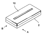
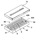
図3は、本発明による複数周波数帯域通過フィルタの第2の実施形態を示す模式的斜視図である。図4は、本実施形態の複数周波数帯域通過フィルタの模式的分解斜視図である。図5は、図3のA矢視模式的部分断面図である。図6は、図3のB矢視模式的断面図である。本実施形態においては、複数周波数帯域通過フィルタは2周波数帯域通過フィルタである。図3〜図6において、図1及び図2におけると同様な部材または部分には、同一の符号が付されている。 FIG. 3 is a schematic perspective view showing a second embodiment of the multi-frequency bandpass filter according to the present invention. FIG. 4 is a schematic exploded perspective view of the multi-frequency bandpass filter of the present embodiment. FIG. 5 is a schematic partial cross-sectional view taken along arrow A in FIG. 6 is a schematic cross-sectional view taken in the direction of arrow B in FIG. In the present embodiment, the multiple frequency bandpass filter is a two-frequency bandpass filter. 3 to 6, the same members or parts as those in FIGS. 1 and 2 are denoted by the same reference numerals.
本実施形態は、基本的には、電磁シールドカバーを備えることを除いて、第1の実施形態と同一である。 This embodiment is basically the same as the first embodiment except that an electromagnetic shield cover is provided.
但し、誘電体ブロック2の第1の面21には、シールド導体9から延びた接続導体91が形成されている。
However, a
電磁シールドカバー10は、誘電体ブロック2の第1の面21を略覆うように配置されている。具体的には、電磁シールドカバー10は、誘電体ブロック2の第1の面21の開放域(導体が形成されていない領域部)から隔てられて該開放域を覆うように配置されており、たとえば厚み0.3mm〜0.8mm程度の金属板を成形したものからなる。電磁シールドカバー10の材質は、導電性であれば良く、例えば鉄系の金属、特に表面をすずめっきした鉄などを用いることができる。電磁シールドカバー10は、誘電体ブロック2の第3の面23〜第6の面26に付された外導体43及び誘電体ブロック2の第1の面21に付された接続導体91に接合されている。この接合には、たとえば半田または導電性接着剤が用いられる。これにより、第1の面(開放域)21からの電波漏洩を抑制し、良好な電磁シールド効果を発揮して、一層高い電気特性を得ることができる。
The
さらに、接続導体91を介して電磁シールドカバー10が接合されているため、スリット8の幅Dが狭い場合でも取り付けが容易で、小型化に寄与する。スリット幅Dに余裕がある場合は、もちろん電磁シールドカバー10をシールド導体9に直接接合しても良い。
Furthermore, since the
尚、図5に示されるように、第1共通電極61には同軸型接続ケーブル12の内部導体が接続されており、該接続ケーブル12によって2周波数帯域通過フィルタが外部回路の一組の入出力端子と接続される。接続ケーブル12の外部導体は、たとえば電磁シールドカバー10に接続される。第2共通電極62についても同様である。
As shown in FIG. 5, the inner conductor of the
2周波数帯域通過フィルタと外部回路との接続方法については、上記の限りではなく、必要に応じて公知の他の方法が用いられ、同軸型の接続コネクタを用いたものでも良いし、リードピンを用いたものでも良い。 The method for connecting the two-frequency bandpass filter and the external circuit is not limited to the above, and other known methods may be used as necessary, using a coaxial connector or using a lead pin. What was there is good.
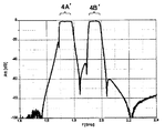
図7は、本実施形態の複数周波数帯域通過フィルタの周波数特性の一例を示すものであり、横軸に周波数をとり、縦軸に減衰量をとって、示している。第1帯域通過フィルタ部4Aにより構成される低域通過フィルタの通過帯域(4A’)は約1.7GHzから1.8GHzであり、第2帯域通過フィルタ部4Bにより構成される高域通過フィルタの通過帯域(4B’)は約1.9GHzから2GHzである。図7より、これら通過帯域以外の周波数帯域は、第1の面21から漏洩する電波が抑制され、良好に減衰していることがわかる。
FIG. 7 shows an example of frequency characteristics of the multi-frequency bandpass filter of the present embodiment. The horizontal axis represents frequency and the vertical axis represents attenuation. The pass band (4A ′) of the low-pass filter configured by the first band-
以上、実施形態を示したが、本発明は上記実施形態に限定されるものでないことはもちろんであり、種々の変更が可能である。たとえば、第1帯域通過フィルタ部4A及び第2帯域通過フィルタ部4Bを構成する共振器数や配列間隔は、適宜変更可能である。第1帯域通過フィルタ部4Aと第2帯域通過フィルタ部4Bとで、共振器数、貫通孔の断面形状が異なっていても良い。各部材の材料についても、実施形態で説明したものに限定されない。
Although the embodiment has been described above, the present invention is not limited to the above embodiment, and various modifications can be made. For example, the number of resonators and the arrangement interval constituting the first band
2 誘電体ブロック
21 第1の面
22 第2の面
23 第3の面
24 第4の面
25 第5の面
26 第6の面
4A 第1帯域通過フィルタ部
40A 第1貫通孔群
41A 第1の貫通孔
42A 第1内導体
43 外導体
44A 第1結合電極
4B 第2帯域通過フィルタ部
40B 第2貫通孔群
41B 第2の貫通孔
42B 第2内導体
44B 第2結合電極
61 第1共通電極
62 第2共通電極
8 スリット
9 シールド導体
91 接続導体
10 電磁シールドカバー
12 同軸型接続ケーブル
2
Claims (4)
該誘電体ブロックを用いて構成される第1帯域通過フィルタ部及び第2帯域通過フィルタ部と、
を含んでなる複数周波数帯域通過フィルタであって、
前記第1帯域通過フィルタ部は、
前記誘電体ブロックに前記第1の面から前記第2の面にかけて形成され、前記第3の面に沿って配列された複数の第1の貫通孔からなる第1貫通孔群と、
前記第1の貫通孔の内面に形成された第1内導体と、
前記第1の面を除く前記誘電体ブロックの外面に形成された外導体と、
前記第1の面にて前記第1内導体から延び、前記第1の貫通孔に対応して形成される共振器同士を結合させる第1結合電極と、
を含んでなり、
前記第2帯域通過フィルタ部は、
前記誘電体ブロックに前記第1の面から前記第2の面にかけて形成され、前記第4の面に沿って配列された複数の第2の貫通孔からなる第2貫通孔群と、
前記第2の貫通孔の内面に形成された第2内導体と、
前記第1の面を除く前記誘電体ブロックの外面に形成された外導体と、
前記第1の面にて前記第2内導体から延び、前記第2の貫通孔に対応して形成される共振器同士を結合させる第2結合電極と、
を含んでなり、
前記第1の面には、前記第1帯域通過フィルタ部の一方端部の共振器及び前記第2帯域通過フィルタ部の一方端部の共振器と結合する第1共通電極と、前記第1帯域通過フィルタ部の他方端部の共振器及び前記第2帯域通過フィルタ部の他方端部の共振器と結合する第2共通電極と、が形成されており、
前記誘電体ブロックには、前記第1貫通孔群と前記第2貫通孔群との間に介在し、前記第1の面から前記第2の面にかけて形成され、前記第3の面及び前記第4の面と略平行に延びたスリットが形成されており、
該スリットの内面には、前記第2の面に形成された前記外導体と接続されたシールド導体が形成されている、
ことを特徴とする、複数周波数帯域通過フィルタ。 A first surface and a second surface that are substantially parallel to each other; and an outer surface that includes a third surface and a fourth surface that are substantially orthogonal to the first surface and the second surface and substantially parallel to each other. Having a dielectric block;
A first bandpass filter unit and a second bandpass filter unit configured using the dielectric block;
A multi-frequency bandpass filter comprising
The first band pass filter unit is:
A first through hole group comprising a plurality of first through holes formed in the dielectric block from the first surface to the second surface and arranged along the third surface;
A first inner conductor formed on the inner surface of the first through hole;
An outer conductor formed on an outer surface of the dielectric block excluding the first surface;
A first coupling electrode extending from the first inner conductor on the first surface and coupling resonators formed corresponding to the first through holes;
Comprising
The second bandpass filter unit is
A second through hole group comprising a plurality of second through holes formed in the dielectric block from the first surface to the second surface and arranged along the fourth surface;
A second inner conductor formed on the inner surface of the second through hole;
An outer conductor formed on an outer surface of the dielectric block excluding the first surface;
A second coupling electrode extending from the second inner conductor on the first surface and coupling resonators formed corresponding to the second through holes;
Comprising
The first surface includes a first common electrode coupled to a resonator at one end of the first bandpass filter unit and a resonator at one end of the second bandpass filter unit, and the first band. A resonator at the other end of the pass filter section and a second common electrode coupled to the resonator at the other end of the second band pass filter section are formed,
The dielectric block is interposed between the first through-hole group and the second through-hole group and is formed from the first surface to the second surface, and the third surface and the second surface A slit extending substantially parallel to the surface of 4 is formed,
On the inner surface of the slit, a shield conductor connected to the outer conductor formed on the second surface is formed.
A multi-frequency bandpass filter characterized by the above.
Priority Applications (1)
| Application Number | Priority Date | Filing Date | Title |
|---|---|---|---|
| JP2011074926A JP2012209826A (en) | 2011-03-30 | 2011-03-30 | Multiple frequency band passing filter |
Applications Claiming Priority (1)
| Application Number | Priority Date | Filing Date | Title |
|---|---|---|---|
| JP2011074926A JP2012209826A (en) | 2011-03-30 | 2011-03-30 | Multiple frequency band passing filter |
Publications (1)
| Publication Number | Publication Date |
|---|---|
| JP2012209826A true JP2012209826A (en) | 2012-10-25 |
Family
ID=47189209
Family Applications (1)
| Application Number | Title | Priority Date | Filing Date |
|---|---|---|---|
| JP2011074926A Pending JP2012209826A (en) | 2011-03-30 | 2011-03-30 | Multiple frequency band passing filter |
Country Status (1)
| Country | Link |
|---|---|
| JP (1) | JP2012209826A (en) |
Cited By (2)
| Publication number | Priority date | Publication date | Assignee | Title |
|---|---|---|---|---|
| WO2021096177A1 (en) * | 2019-11-13 | 2021-05-20 | 주식회사 케이엠더블유 | Dielectric ceramic filter |
| KR20210058690A (en) * | 2019-11-13 | 2021-05-24 | 주식회사 케이엠더블유 | Dielectric ceramic filter |
Citations (5)
| Publication number | Priority date | Publication date | Assignee | Title |
|---|---|---|---|---|
| JPS6247201A (en) * | 1985-08-23 | 1987-02-28 | Murata Mfg Co Ltd | Shared dielectric block |
| US5191305A (en) * | 1991-07-02 | 1993-03-02 | Interstate Electronics Corporation | Multiple bandpass filter |
| JP2002135001A (en) * | 2000-10-26 | 2002-05-10 | Tdk Corp | Resin base body filter |
| JP2002252501A (en) * | 2001-02-23 | 2002-09-06 | Yokowo Co Ltd | Bandpass filter |
| JP2010239414A (en) * | 2009-03-31 | 2010-10-21 | Ube Ind Ltd | Dielectric resonance component and mounting structure using the same |
-
2011
- 2011-03-30 JP JP2011074926A patent/JP2012209826A/en active Pending
Patent Citations (5)
| Publication number | Priority date | Publication date | Assignee | Title |
|---|---|---|---|---|
| JPS6247201A (en) * | 1985-08-23 | 1987-02-28 | Murata Mfg Co Ltd | Shared dielectric block |
| US5191305A (en) * | 1991-07-02 | 1993-03-02 | Interstate Electronics Corporation | Multiple bandpass filter |
| JP2002135001A (en) * | 2000-10-26 | 2002-05-10 | Tdk Corp | Resin base body filter |
| JP2002252501A (en) * | 2001-02-23 | 2002-09-06 | Yokowo Co Ltd | Bandpass filter |
| JP2010239414A (en) * | 2009-03-31 | 2010-10-21 | Ube Ind Ltd | Dielectric resonance component and mounting structure using the same |
Cited By (5)
| Publication number | Priority date | Publication date | Assignee | Title |
|---|---|---|---|---|
| WO2021096177A1 (en) * | 2019-11-13 | 2021-05-20 | 주식회사 케이엠더블유 | Dielectric ceramic filter |
| KR20210058690A (en) * | 2019-11-13 | 2021-05-24 | 주식회사 케이엠더블유 | Dielectric ceramic filter |
| KR102437331B1 (en) * | 2019-11-13 | 2022-08-30 | 주식회사 케이엠더블유 | Dielectric ceramic filter |
| KR20220122949A (en) * | 2019-11-13 | 2022-09-05 | 주식회사 케이엠더블유 | Dielectric ceramic filter |
| KR102613545B1 (en) | 2019-11-13 | 2023-12-14 | 주식회사 케이엠더블유 | Dielectric ceramic filter |
Similar Documents
| Publication | Publication Date | Title |
|---|---|---|
| US10110196B2 (en) | Electronic component | |
| US8294532B2 (en) | Duplex filter comprised of dielectric cores having at least one wall extending above a top surface thereof for isolating through hole resonators | |
| JP2007013962A (en) | Multilayer band pass filter | |
| CN112889182B (en) | Dielectric filter and communication equipment | |
| US20140145798A1 (en) | Electronic component | |
| JP6563164B1 (en) | High frequency filter | |
| JP4148423B2 (en) | Dielectric device | |
| KR100866978B1 (en) | Te mode dielectric duplexer | |
| JP2012209826A (en) | Multiple frequency band passing filter | |
| JP5703917B2 (en) | Dielectric resonant component | |
| US8400236B2 (en) | Electronic component | |
| JP2003110306A (en) | Dielectric device | |
| JP2018093473A (en) | Bandpass filter | |
| JP6287031B2 (en) | Dielectric resonant component | |
| WO2017085936A1 (en) | Dielectric filter unit and communication device | |
| US9520634B2 (en) | Resonance device | |
| JP2020072450A (en) | Dielectric resonance component | |
| JP6674684B2 (en) | Low pass filter | |
| JP5299685B2 (en) | Dielectric duplexer | |
| KR101681899B1 (en) | Dielectric filter | |
| KR101439420B1 (en) | Resonator and filter having the same | |
| KR101628696B1 (en) | Cavity type low pass filter | |
| US20220407489A1 (en) | High frequency filter | |
| CN108736111B (en) | Filter with a filter element having a plurality of filter elements | |
| JP3848542B2 (en) | Band pass filter |
Legal Events
| Date | Code | Title | Description |
|---|---|---|---|
| A621 | Written request for application examination |
Free format text: JAPANESE INTERMEDIATE CODE: A621 Effective date: 20140131 |
|
| A977 | Report on retrieval |
Free format text: JAPANESE INTERMEDIATE CODE: A971007 Effective date: 20140910 |
|
| A131 | Notification of reasons for refusal |
Free format text: JAPANESE INTERMEDIATE CODE: A131 Effective date: 20141007 |
|
| A521 | Written amendment |
Free format text: JAPANESE INTERMEDIATE CODE: A523 Effective date: 20141105 |
|
| A131 | Notification of reasons for refusal |
Free format text: JAPANESE INTERMEDIATE CODE: A131 Effective date: 20150303 |
|
| A02 | Decision of refusal |
Free format text: JAPANESE INTERMEDIATE CODE: A02 Effective date: 20150625 |