JP2012189600A - Encoded microparticles - Google Patents
Encoded microparticles Download PDFInfo
- Publication number
- JP2012189600A JP2012189600A JP2012088799A JP2012088799A JP2012189600A JP 2012189600 A JP2012189600 A JP 2012189600A JP 2012088799 A JP2012088799 A JP 2012088799A JP 2012088799 A JP2012088799 A JP 2012088799A JP 2012189600 A JP2012189600 A JP 2012189600A
- Authority
- JP
- Japan
- Prior art keywords
- microparticle
- microparticles
- code
- encoded
- wafer
- Prior art date
- Legal status (The legal status is an assumption and is not a legal conclusion. Google has not performed a legal analysis and makes no representation as to the accuracy of the status listed.)
- Granted
Links
- 239000011859 microparticle Substances 0.000 title claims abstract description 1761
- 238000000034 method Methods 0.000 claims abstract description 468
- 239000000463 material Substances 0.000 claims abstract description 388
- 238000004166 bioassay Methods 0.000 claims abstract description 42
- 239000002245 particle Substances 0.000 claims description 615
- 235000012431 wafers Nutrition 0.000 claims description 403
- 239000012780 transparent material Substances 0.000 claims description 320
- 239000010410 layer Substances 0.000 claims description 256
- 239000000758 substrate Substances 0.000 claims description 220
- 239000000523 sample Substances 0.000 claims description 179
- VYPSYNLAJGMNEJ-UHFFFAOYSA-N Silicium dioxide Chemical compound O=[Si]=O VYPSYNLAJGMNEJ-UHFFFAOYSA-N 0.000 claims description 135
- 238000004519 manufacturing process Methods 0.000 claims description 135
- XUIMIQQOPSSXEZ-UHFFFAOYSA-N Silicon Chemical compound [Si] XUIMIQQOPSSXEZ-UHFFFAOYSA-N 0.000 claims description 128
- 229910052710 silicon Inorganic materials 0.000 claims description 128
- 239000010703 silicon Substances 0.000 claims description 128
- 239000011521 glass Substances 0.000 claims description 119
- 238000001514 detection method Methods 0.000 claims description 112
- 230000008569 process Effects 0.000 claims description 86
- 108090000623 proteins and genes Proteins 0.000 claims description 72
- 229920002120 photoresistant polymer Polymers 0.000 claims description 71
- 239000000377 silicon dioxide Substances 0.000 claims description 65
- 235000012239 silicon dioxide Nutrition 0.000 claims description 63
- 239000002356 single layer Substances 0.000 claims description 60
- 239000007788 liquid Substances 0.000 claims description 58
- 238000002493 microarray Methods 0.000 claims description 54
- 238000005530 etching Methods 0.000 claims description 52
- 238000000059 patterning Methods 0.000 claims description 46
- 102000004169 proteins and genes Human genes 0.000 claims description 46
- 238000003384 imaging method Methods 0.000 claims description 43
- 230000003287 optical effect Effects 0.000 claims description 41
- 102000039446 nucleic acids Human genes 0.000 claims description 39
- 108020004707 nucleic acids Proteins 0.000 claims description 39
- 150000007523 nucleic acids Chemical group 0.000 claims description 39
- 238000000206 photolithography Methods 0.000 claims description 39
- 238000000151 deposition Methods 0.000 claims description 38
- 230000005653 Brownian motion process Effects 0.000 claims description 37
- 238000005537 brownian motion Methods 0.000 claims description 37
- 108020004414 DNA Proteins 0.000 claims description 33
- 230000007246 mechanism Effects 0.000 claims description 32
- 239000012530 fluid Substances 0.000 claims description 31
- 238000012360 testing method Methods 0.000 claims description 31
- WGTYBPLFGIVFAS-UHFFFAOYSA-M tetramethylammonium hydroxide Chemical compound [OH-].C[N+](C)(C)C WGTYBPLFGIVFAS-UHFFFAOYSA-M 0.000 claims description 30
- 238000004458 analytical method Methods 0.000 claims description 26
- 230000005540 biological transmission Effects 0.000 claims description 26
- 230000000295 complement effect Effects 0.000 claims description 26
- 239000004065 semiconductor Substances 0.000 claims description 25
- OAICVXFJPJFONN-UHFFFAOYSA-N Phosphorus Chemical compound [P] OAICVXFJPJFONN-UHFFFAOYSA-N 0.000 claims description 24
- 229910021417 amorphous silicon Inorganic materials 0.000 claims description 24
- VYZAMTAEIAYCRO-UHFFFAOYSA-N Chromium Chemical compound [Cr] VYZAMTAEIAYCRO-UHFFFAOYSA-N 0.000 claims description 22
- 239000003298 DNA probe Substances 0.000 claims description 22
- 108020004518 RNA Probes Proteins 0.000 claims description 22
- 239000003391 RNA probe Substances 0.000 claims description 22
- 239000011368 organic material Substances 0.000 claims description 22
- 108091032973 (ribonucleotides)n+m Proteins 0.000 claims description 21
- 108091034117 Oligonucleotide Proteins 0.000 claims description 21
- 239000000696 magnetic material Substances 0.000 claims description 21
- 229910052723 transition metal Inorganic materials 0.000 claims description 21
- 239000000872 buffer Substances 0.000 claims description 20
- 238000001429 visible spectrum Methods 0.000 claims description 19
- 150000001875 compounds Chemical class 0.000 claims description 18
- 230000005670 electromagnetic radiation Effects 0.000 claims description 18
- 238000001459 lithography Methods 0.000 claims description 18
- 150000003624 transition metals Chemical class 0.000 claims description 18
- 229910052581 Si3N4 Inorganic materials 0.000 claims description 17
- HQVNEWCFYHHQES-UHFFFAOYSA-N silicon nitride Chemical compound N12[Si]34N5[Si]62N3[Si]51N64 HQVNEWCFYHHQES-UHFFFAOYSA-N 0.000 claims description 17
- -1 transition metal nitride Chemical class 0.000 claims description 17
- 230000027455 binding Effects 0.000 claims description 16
- 229910052751 metal Inorganic materials 0.000 claims description 16
- 239000002184 metal Substances 0.000 claims description 16
- 229910052752 metalloid Inorganic materials 0.000 claims description 16
- 150000002738 metalloids Chemical class 0.000 claims description 16
- 239000011324 bead Substances 0.000 claims description 15
- 238000009792 diffusion process Methods 0.000 claims description 15
- 238000007373 indentation Methods 0.000 claims description 15
- 229910021420 polycrystalline silicon Inorganic materials 0.000 claims description 15
- ZOXJGFHDIHLPTG-UHFFFAOYSA-N Boron Chemical compound [B] ZOXJGFHDIHLPTG-UHFFFAOYSA-N 0.000 claims description 14
- 229910052796 boron Inorganic materials 0.000 claims description 14
- 229910052804 chromium Inorganic materials 0.000 claims description 14
- 239000011651 chromium Substances 0.000 claims description 14
- 229910052698 phosphorus Inorganic materials 0.000 claims description 14
- 239000011574 phosphorus Substances 0.000 claims description 14
- 229920005591 polysilicon Polymers 0.000 claims description 14
- 239000010936 titanium Substances 0.000 claims description 14
- 229910052719 titanium Inorganic materials 0.000 claims description 14
- 238000002834 transmittance Methods 0.000 claims description 14
- 229910052721 tungsten Inorganic materials 0.000 claims description 14
- 230000036961 partial effect Effects 0.000 claims description 13
- 102000004190 Enzymes Human genes 0.000 claims description 12
- 108090000790 Enzymes Proteins 0.000 claims description 12
- PXHVJJICTQNCMI-UHFFFAOYSA-N Nickel Chemical compound [Ni] PXHVJJICTQNCMI-UHFFFAOYSA-N 0.000 claims description 12
- RTAQQCXQSZGOHL-UHFFFAOYSA-N Titanium Chemical compound [Ti] RTAQQCXQSZGOHL-UHFFFAOYSA-N 0.000 claims description 12
- 239000003814 drug Substances 0.000 claims description 12
- 229910010272 inorganic material Inorganic materials 0.000 claims description 12
- 239000011147 inorganic material Substances 0.000 claims description 12
- 239000003446 ligand Substances 0.000 claims description 12
- 239000010937 tungsten Substances 0.000 claims description 12
- JLCPHMBAVCMARE-UHFFFAOYSA-N [3-[[3-[[3-[[3-[[3-[[3-[[3-[[3-[[3-[[3-[[3-[[5-(2-amino-6-oxo-1H-purin-9-yl)-3-[[3-[[3-[[3-[[3-[[3-[[5-(2-amino-6-oxo-1H-purin-9-yl)-3-[[5-(2-amino-6-oxo-1H-purin-9-yl)-3-hydroxyoxolan-2-yl]methoxy-hydroxyphosphoryl]oxyoxolan-2-yl]methoxy-hydroxyphosphoryl]oxy-5-(5-methyl-2,4-dioxopyrimidin-1-yl)oxolan-2-yl]methoxy-hydroxyphosphoryl]oxy-5-(6-aminopurin-9-yl)oxolan-2-yl]methoxy-hydroxyphosphoryl]oxy-5-(6-aminopurin-9-yl)oxolan-2-yl]methoxy-hydroxyphosphoryl]oxy-5-(6-aminopurin-9-yl)oxolan-2-yl]methoxy-hydroxyphosphoryl]oxy-5-(6-aminopurin-9-yl)oxolan-2-yl]methoxy-hydroxyphosphoryl]oxyoxolan-2-yl]methoxy-hydroxyphosphoryl]oxy-5-(5-methyl-2,4-dioxopyrimidin-1-yl)oxolan-2-yl]methoxy-hydroxyphosphoryl]oxy-5-(4-amino-2-oxopyrimidin-1-yl)oxolan-2-yl]methoxy-hydroxyphosphoryl]oxy-5-(5-methyl-2,4-dioxopyrimidin-1-yl)oxolan-2-yl]methoxy-hydroxyphosphoryl]oxy-5-(5-methyl-2,4-dioxopyrimidin-1-yl)oxolan-2-yl]methoxy-hydroxyphosphoryl]oxy-5-(6-aminopurin-9-yl)oxolan-2-yl]methoxy-hydroxyphosphoryl]oxy-5-(6-aminopurin-9-yl)oxolan-2-yl]methoxy-hydroxyphosphoryl]oxy-5-(4-amino-2-oxopyrimidin-1-yl)oxolan-2-yl]methoxy-hydroxyphosphoryl]oxy-5-(4-amino-2-oxopyrimidin-1-yl)oxolan-2-yl]methoxy-hydroxyphosphoryl]oxy-5-(4-amino-2-oxopyrimidin-1-yl)oxolan-2-yl]methoxy-hydroxyphosphoryl]oxy-5-(6-aminopurin-9-yl)oxolan-2-yl]methoxy-hydroxyphosphoryl]oxy-5-(4-amino-2-oxopyrimidin-1-yl)oxolan-2-yl]methyl [5-(6-aminopurin-9-yl)-2-(hydroxymethyl)oxolan-3-yl] hydrogen phosphate Polymers Cc1cn(C2CC(OP(O)(=O)OCC3OC(CC3OP(O)(=O)OCC3OC(CC3O)n3cnc4c3nc(N)[nH]c4=O)n3cnc4c3nc(N)[nH]c4=O)C(COP(O)(=O)OC3CC(OC3COP(O)(=O)OC3CC(OC3COP(O)(=O)OC3CC(OC3COP(O)(=O)OC3CC(OC3COP(O)(=O)OC3CC(OC3COP(O)(=O)OC3CC(OC3COP(O)(=O)OC3CC(OC3COP(O)(=O)OC3CC(OC3COP(O)(=O)OC3CC(OC3COP(O)(=O)OC3CC(OC3COP(O)(=O)OC3CC(OC3COP(O)(=O)OC3CC(OC3COP(O)(=O)OC3CC(OC3COP(O)(=O)OC3CC(OC3COP(O)(=O)OC3CC(OC3COP(O)(=O)OC3CC(OC3COP(O)(=O)OC3CC(OC3CO)n3cnc4c(N)ncnc34)n3ccc(N)nc3=O)n3cnc4c(N)ncnc34)n3ccc(N)nc3=O)n3ccc(N)nc3=O)n3ccc(N)nc3=O)n3cnc4c(N)ncnc34)n3cnc4c(N)ncnc34)n3cc(C)c(=O)[nH]c3=O)n3cc(C)c(=O)[nH]c3=O)n3ccc(N)nc3=O)n3cc(C)c(=O)[nH]c3=O)n3cnc4c3nc(N)[nH]c4=O)n3cnc4c(N)ncnc34)n3cnc4c(N)ncnc34)n3cnc4c(N)ncnc34)n3cnc4c(N)ncnc34)O2)c(=O)[nH]c1=O JLCPHMBAVCMARE-UHFFFAOYSA-N 0.000 claims description 10
- 239000000919 ceramic Substances 0.000 claims description 10
- 229940079593 drug Drugs 0.000 claims description 10
- 229910052750 molybdenum Inorganic materials 0.000 claims description 10
- 238000011002 quantification Methods 0.000 claims description 10
- WFKWXMTUELFFGS-UHFFFAOYSA-N tungsten Chemical compound [W] WFKWXMTUELFFGS-UHFFFAOYSA-N 0.000 claims description 10
- 238000004590 computer program Methods 0.000 claims description 9
- 238000005406 washing Methods 0.000 claims description 9
- XEEYBQQBJWHFJM-UHFFFAOYSA-N Iron Chemical compound [Fe] XEEYBQQBJWHFJM-UHFFFAOYSA-N 0.000 claims description 8
- ZOKXTWBITQBERF-UHFFFAOYSA-N Molybdenum Chemical compound [Mo] ZOKXTWBITQBERF-UHFFFAOYSA-N 0.000 claims description 8
- 229910052782 aluminium Inorganic materials 0.000 claims description 8
- XAGFODPZIPBFFR-UHFFFAOYSA-N aluminium Chemical compound [Al] XAGFODPZIPBFFR-UHFFFAOYSA-N 0.000 claims description 8
- 239000011248 coating agent Substances 0.000 claims description 8
- 238000000576 coating method Methods 0.000 claims description 8
- 230000003993 interaction Effects 0.000 claims description 8
- 238000002156 mixing Methods 0.000 claims description 8
- 239000011733 molybdenum Substances 0.000 claims description 8
- 108090000765 processed proteins & peptides Proteins 0.000 claims description 8
- 239000004816 latex Substances 0.000 claims description 7
- 229920000126 latex Polymers 0.000 claims description 7
- 229920000642 polymer Polymers 0.000 claims description 7
- 102000004196 processed proteins & peptides Human genes 0.000 claims description 7
- KPUWHANPEXNPJT-UHFFFAOYSA-N disiloxane Chemical class [SiH3]O[SiH3] KPUWHANPEXNPJT-UHFFFAOYSA-N 0.000 claims description 6
- 229910021421 monocrystalline silicon Inorganic materials 0.000 claims description 6
- 229910052759 nickel Inorganic materials 0.000 claims description 6
- 229910052715 tantalum Inorganic materials 0.000 claims description 6
- GUVRBAGPIYLISA-UHFFFAOYSA-N tantalum atom Chemical compound [Ta] GUVRBAGPIYLISA-UHFFFAOYSA-N 0.000 claims description 6
- 239000010409 thin film Substances 0.000 claims description 6
- 229910017052 cobalt Inorganic materials 0.000 claims description 5
- 239000010941 cobalt Substances 0.000 claims description 5
- GUTLYIVDDKVIGB-UHFFFAOYSA-N cobalt atom Chemical compound [Co] GUTLYIVDDKVIGB-UHFFFAOYSA-N 0.000 claims description 5
- 239000010408 film Substances 0.000 claims description 5
- 239000002073 nanorod Substances 0.000 claims description 5
- 229920001184 polypeptide Polymers 0.000 claims description 5
- 239000002096 quantum dot Substances 0.000 claims description 5
- 239000003822 epoxy resin Substances 0.000 claims description 4
- 229910052742 iron Inorganic materials 0.000 claims description 4
- 229920000647 polyepoxide Polymers 0.000 claims description 4
- 229910000314 transition metal oxide Inorganic materials 0.000 claims description 4
- 239000004642 Polyimide Substances 0.000 claims description 3
- 229910000577 Silicon-germanium Inorganic materials 0.000 claims description 3
- 238000004049 embossing Methods 0.000 claims description 3
- 229910052732 germanium Inorganic materials 0.000 claims description 3
- GNPVGFCGXDBREM-UHFFFAOYSA-N germanium atom Chemical compound [Ge] GNPVGFCGXDBREM-UHFFFAOYSA-N 0.000 claims description 3
- 239000002923 metal particle Substances 0.000 claims description 3
- 239000002105 nanoparticle Substances 0.000 claims description 3
- 229920001721 polyimide Polymers 0.000 claims description 3
- 238000000159 protein binding assay Methods 0.000 claims description 3
- 238000001228 spectrum Methods 0.000 claims description 3
- 239000012620 biological material Substances 0.000 claims 27
- 239000002777 nucleoside Substances 0.000 claims 16
- 150000003833 nucleoside derivatives Chemical class 0.000 claims 13
- 108020003215 DNA Probes Proteins 0.000 claims 12
- 239000012491 analyte Substances 0.000 claims 6
- 125000003835 nucleoside group Chemical group 0.000 claims 3
- 239000007787 solid Substances 0.000 claims 3
- 239000002344 surface layer Substances 0.000 claims 3
- 239000011149 active material Substances 0.000 claims 2
- 239000000470 constituent Substances 0.000 claims 2
- 230000003100 immobilizing effect Effects 0.000 claims 2
- 125000006850 spacer group Chemical group 0.000 claims 2
- 229910001218 Gallium arsenide Inorganic materials 0.000 claims 1
- BQCADISMDOOEFD-UHFFFAOYSA-N Silver Chemical compound [Ag] BQCADISMDOOEFD-UHFFFAOYSA-N 0.000 claims 1
- 238000010521 absorption reaction Methods 0.000 claims 1
- 239000007853 buffer solution Substances 0.000 claims 1
- 238000005229 chemical vapour deposition Methods 0.000 claims 1
- 238000005520 cutting process Methods 0.000 claims 1
- 238000000799 fluorescence microscopy Methods 0.000 claims 1
- PCHJSUWPFVWCPO-UHFFFAOYSA-N gold Chemical compound [Au] PCHJSUWPFVWCPO-UHFFFAOYSA-N 0.000 claims 1
- 229910052737 gold Inorganic materials 0.000 claims 1
- 239000010931 gold Substances 0.000 claims 1
- 239000012535 impurity Substances 0.000 claims 1
- 230000009149 molecular binding Effects 0.000 claims 1
- 238000001579 optical reflectometry Methods 0.000 claims 1
- 229920003229 poly(methyl methacrylate) Polymers 0.000 claims 1
- 239000004926 polymethyl methacrylate Substances 0.000 claims 1
- 239000002243 precursor Substances 0.000 claims 1
- 229910052814 silicon oxide Inorganic materials 0.000 claims 1
- 229910052709 silver Inorganic materials 0.000 claims 1
- 239000004332 silver Substances 0.000 claims 1
- 150000003384 small molecules Chemical class 0.000 claims 1
- 238000003556 assay Methods 0.000 description 62
- 210000004027 cell Anatomy 0.000 description 48
- 238000010586 diagram Methods 0.000 description 39
- 239000000203 mixture Substances 0.000 description 30
- 238000009396 hybridization Methods 0.000 description 26
- 239000000126 substance Substances 0.000 description 26
- 238000005234 chemical deposition Methods 0.000 description 24
- 238000000018 DNA microarray Methods 0.000 description 22
- 230000014509 gene expression Effects 0.000 description 22
- 238000012545 processing Methods 0.000 description 20
- 238000011160 research Methods 0.000 description 20
- KWYUFKZDYYNOTN-UHFFFAOYSA-M Potassium hydroxide Chemical compound [OH-].[K+] KWYUFKZDYYNOTN-UHFFFAOYSA-M 0.000 description 18
- 238000005516 engineering process Methods 0.000 description 18
- 230000008859 change Effects 0.000 description 16
- 238000001878 scanning electron micrograph Methods 0.000 description 16
- 230000015572 biosynthetic process Effects 0.000 description 15
- 230000008901 benefit Effects 0.000 description 14
- 238000002073 fluorescence micrograph Methods 0.000 description 14
- 239000007789 gas Substances 0.000 description 14
- 238000000926 separation method Methods 0.000 description 14
- 238000013461 design Methods 0.000 description 12
- 238000011161 development Methods 0.000 description 12
- 230000005284 excitation Effects 0.000 description 12
- 238000005286 illumination Methods 0.000 description 12
- 238000012634 optical imaging Methods 0.000 description 12
- 241000894007 species Species 0.000 description 12
- 238000003491 array Methods 0.000 description 11
- 230000002776 aggregation Effects 0.000 description 10
- 238000004220 aggregation Methods 0.000 description 10
- 230000021615 conjugation Effects 0.000 description 10
- 230000008021 deposition Effects 0.000 description 10
- 201000010099 disease Diseases 0.000 description 10
- 208000037265 diseases, disorders, signs and symptoms Diseases 0.000 description 10
- 230000005484 gravity Effects 0.000 description 10
- 244000052769 pathogen Species 0.000 description 10
- 238000002360 preparation method Methods 0.000 description 10
- 239000000047 product Substances 0.000 description 10
- 230000002068 genetic effect Effects 0.000 description 9
- 102000003688 G-Protein-Coupled Receptors Human genes 0.000 description 8
- 108090000045 G-Protein-Coupled Receptors Proteins 0.000 description 8
- 206010028980 Neoplasm Diseases 0.000 description 8
- 201000011510 cancer Diseases 0.000 description 8
- 238000006243 chemical reaction Methods 0.000 description 8
- 239000002299 complementary DNA Substances 0.000 description 8
- 239000002131 composite material Substances 0.000 description 8
- 230000000694 effects Effects 0.000 description 8
- 238000002372 labelling Methods 0.000 description 8
- 239000004005 microsphere Substances 0.000 description 8
- 238000005289 physical deposition Methods 0.000 description 8
- 238000001020 plasma etching Methods 0.000 description 8
- 102000005962 receptors Human genes 0.000 description 8
- 108020003175 receptors Proteins 0.000 description 8
- 238000012552 review Methods 0.000 description 8
- 238000007429 general method Methods 0.000 description 7
- QTBSBXVTEAMEQO-UHFFFAOYSA-N Acetic acid Chemical compound CC(O)=O QTBSBXVTEAMEQO-UHFFFAOYSA-N 0.000 description 6
- 206010006187 Breast cancer Diseases 0.000 description 6
- 208000026310 Breast neoplasm Diseases 0.000 description 6
- 229910004298 SiO 2 Inorganic materials 0.000 description 6
- HEMHJVSKTPXQMS-UHFFFAOYSA-M Sodium hydroxide Chemical compound [OH-].[Na+] HEMHJVSKTPXQMS-UHFFFAOYSA-M 0.000 description 6
- 230000000052 comparative effect Effects 0.000 description 6
- 238000002508 contact lithography Methods 0.000 description 6
- 238000001312 dry etching Methods 0.000 description 6
- 238000011156 evaluation Methods 0.000 description 6
- 238000010195 expression analysis Methods 0.000 description 6
- 238000002866 fluorescence resonance energy transfer Methods 0.000 description 6
- 238000003018 immunoassay Methods 0.000 description 6
- 230000006872 improvement Effects 0.000 description 6
- 230000000670 limiting effect Effects 0.000 description 6
- 230000033001 locomotion Effects 0.000 description 6
- 239000012071 phase Substances 0.000 description 6
- 230000005855 radiation Effects 0.000 description 6
- 238000001039 wet etching Methods 0.000 description 6
- 229910052727 yttrium Inorganic materials 0.000 description 6
- 238000012544 monitoring process Methods 0.000 description 5
- 230000004044 response Effects 0.000 description 5
- 238000003786 synthesis reaction Methods 0.000 description 5
- 108020004465 16S ribosomal RNA Proteins 0.000 description 4
- 241000251468 Actinopterygii Species 0.000 description 4
- 108700028369 Alleles Proteins 0.000 description 4
- 108091032955 Bacterial small RNA Proteins 0.000 description 4
- 108020004635 Complementary DNA Proteins 0.000 description 4
- 241000196324 Embryophyta Species 0.000 description 4
- KRHYYFGTRYWZRS-UHFFFAOYSA-N Fluorane Chemical compound F KRHYYFGTRYWZRS-UHFFFAOYSA-N 0.000 description 4
- MHAJPDPJQMAIIY-UHFFFAOYSA-N Hydrogen peroxide Chemical compound OO MHAJPDPJQMAIIY-UHFFFAOYSA-N 0.000 description 4
- 102000016267 Leptin Human genes 0.000 description 4
- 108010092277 Leptin Proteins 0.000 description 4
- 108010070047 Notch Receptors Proteins 0.000 description 4
- 102000005650 Notch Receptors Human genes 0.000 description 4
- 239000004793 Polystyrene Substances 0.000 description 4
- 238000005275 alloying Methods 0.000 description 4
- 238000013459 approach Methods 0.000 description 4
- 238000010364 biochemical engineering Methods 0.000 description 4
- 239000012472 biological sample Substances 0.000 description 4
- 210000004556 brain Anatomy 0.000 description 4
- 238000010804 cDNA synthesis Methods 0.000 description 4
- YCIMNLLNPGFGHC-UHFFFAOYSA-N catechol Chemical compound OC1=CC=CC=C1O YCIMNLLNPGFGHC-UHFFFAOYSA-N 0.000 description 4
- 238000012512 characterization method Methods 0.000 description 4
- 239000003795 chemical substances by application Substances 0.000 description 4
- 238000002487 chromatin immunoprecipitation Methods 0.000 description 4
- 238000004140 cleaning Methods 0.000 description 4
- 230000007613 environmental effect Effects 0.000 description 4
- 238000002474 experimental method Methods 0.000 description 4
- 239000000284 extract Substances 0.000 description 4
- 238000000684 flow cytometry Methods 0.000 description 4
- 238000003205 genotyping method Methods 0.000 description 4
- 150000004676 glycans Chemical class 0.000 description 4
- 229910052735 hafnium Inorganic materials 0.000 description 4
- 150000004820 halides Chemical class 0.000 description 4
- NOESYZHRGYRDHS-UHFFFAOYSA-N insulin Chemical compound N1C(=O)C(NC(=O)C(CCC(N)=O)NC(=O)C(CCC(O)=O)NC(=O)C(C(C)C)NC(=O)C(NC(=O)CN)C(C)CC)CSSCC(C(NC(CO)C(=O)NC(CC(C)C)C(=O)NC(CC=2C=CC(O)=CC=2)C(=O)NC(CCC(N)=O)C(=O)NC(CC(C)C)C(=O)NC(CCC(O)=O)C(=O)NC(CC(N)=O)C(=O)NC(CC=2C=CC(O)=CC=2)C(=O)NC(CSSCC(NC(=O)C(C(C)C)NC(=O)C(CC(C)C)NC(=O)C(CC=2C=CC(O)=CC=2)NC(=O)C(CC(C)C)NC(=O)C(C)NC(=O)C(CCC(O)=O)NC(=O)C(C(C)C)NC(=O)C(CC(C)C)NC(=O)C(CC=2NC=NC=2)NC(=O)C(CO)NC(=O)CNC2=O)C(=O)NCC(=O)NC(CCC(O)=O)C(=O)NC(CCCNC(N)=N)C(=O)NCC(=O)NC(CC=3C=CC=CC=3)C(=O)NC(CC=3C=CC=CC=3)C(=O)NC(CC=3C=CC(O)=CC=3)C(=O)NC(C(C)O)C(=O)N3C(CCC3)C(=O)NC(CCCCN)C(=O)NC(C)C(O)=O)C(=O)NC(CC(N)=O)C(O)=O)=O)NC(=O)C(C(C)CC)NC(=O)C(CO)NC(=O)C(C(C)O)NC(=O)C1CSSCC2NC(=O)C(CC(C)C)NC(=O)C(NC(=O)C(CCC(N)=O)NC(=O)C(CC(N)=O)NC(=O)C(NC(=O)C(N)CC=1C=CC=CC=1)C(C)C)CC1=CN=CN1 NOESYZHRGYRDHS-UHFFFAOYSA-N 0.000 description 4
- NRYBAZVQPHGZNS-ZSOCWYAHSA-N leptin Chemical compound O=C([C@H](CO)NC(=O)[C@H](CC(C)C)NC(=O)[C@H](CC(O)=O)NC(=O)[C@H](CC(C)C)NC(=O)[C@H](CCC(N)=O)NC(=O)[C@H](CC=1C2=CC=CC=C2NC=1)NC(=O)[C@H](CC(C)C)NC(=O)[C@@H](NC(=O)[C@H](CC(O)=O)NC(=O)[C@H](CCC(N)=O)NC(=O)[C@H](CC(C)C)NC(=O)[C@H](CO)NC(=O)CNC(=O)[C@H](CCC(N)=O)NC(=O)[C@@H](N)CC(C)C)CCSC)N1CCC[C@H]1C(=O)NCC(=O)N[C@@H](CS)C(O)=O NRYBAZVQPHGZNS-ZSOCWYAHSA-N 0.000 description 4
- 229940039781 leptin Drugs 0.000 description 4
- 235000020281 long black Nutrition 0.000 description 4
- 230000001404 mediated effect Effects 0.000 description 4
- 239000012528 membrane Substances 0.000 description 4
- 108020004999 messenger RNA Proteins 0.000 description 4
- 230000011987 methylation Effects 0.000 description 4
- 238000007069 methylation reaction Methods 0.000 description 4
- 239000011325 microbead Substances 0.000 description 4
- 238000001000 micrograph Methods 0.000 description 4
- 230000004048 modification Effects 0.000 description 4
- 238000012986 modification Methods 0.000 description 4
- 239000003068 molecular probe Substances 0.000 description 4
- 229910052758 niobium Inorganic materials 0.000 description 4
- 239000010955 niobium Substances 0.000 description 4
- 150000004767 nitrides Chemical class 0.000 description 4
- 238000005457 optimization Methods 0.000 description 4
- 230000001717 pathogenic effect Effects 0.000 description 4
- 239000004033 plastic Substances 0.000 description 4
- 238000005498 polishing Methods 0.000 description 4
- 229920002223 polystyrene Polymers 0.000 description 4
- 238000003498 protein array Methods 0.000 description 4
- 239000010453 quartz Substances 0.000 description 4
- 230000002285 radioactive effect Effects 0.000 description 4
- 230000002829 reductive effect Effects 0.000 description 4
- 230000001105 regulatory effect Effects 0.000 description 4
- CPRMKOQKXYSDML-UHFFFAOYSA-M rubidium hydroxide Chemical compound [OH-].[Rb+] CPRMKOQKXYSDML-UHFFFAOYSA-M 0.000 description 4
- 238000012163 sequencing technique Methods 0.000 description 4
- 239000002904 solvent Substances 0.000 description 4
- 230000002269 spontaneous effect Effects 0.000 description 4
- 239000006228 supernatant Substances 0.000 description 4
- 229910052720 vanadium Inorganic materials 0.000 description 4
- 229910052726 zirconium Inorganic materials 0.000 description 4
- 108020005187 Oligonucleotide Probes Proteins 0.000 description 3
- 239000007850 fluorescent dye Substances 0.000 description 3
- 238000002966 oligonucleotide array Methods 0.000 description 3
- 239000002751 oligonucleotide probe Substances 0.000 description 3
- 230000037361 pathway Effects 0.000 description 3
- 102000040650 (ribonucleotides)n+m Human genes 0.000 description 2
- 108020005544 Antisense RNA Proteins 0.000 description 2
- 241000219194 Arabidopsis Species 0.000 description 2
- 244000063299 Bacillus subtilis Species 0.000 description 2
- 235000014469 Bacillus subtilis Nutrition 0.000 description 2
- 229910014265 BrCl Inorganic materials 0.000 description 2
- 102000014914 Carrier Proteins Human genes 0.000 description 2
- 230000004544 DNA amplification Effects 0.000 description 2
- 230000007067 DNA methylation Effects 0.000 description 2
- 241000255925 Diptera Species 0.000 description 2
- 241000255581 Drosophila <fruit fly, genus> Species 0.000 description 2
- 241000588724 Escherichia coli Species 0.000 description 2
- PIICEJLVQHRZGT-UHFFFAOYSA-N Ethylenediamine Chemical compound NCCN PIICEJLVQHRZGT-UHFFFAOYSA-N 0.000 description 2
- 108010058643 Fungal Proteins Proteins 0.000 description 2
- 108091092584 GDNA Proteins 0.000 description 2
- 108010033040 Histones Proteins 0.000 description 2
- 108010001336 Horseradish Peroxidase Proteins 0.000 description 2
- 102000004877 Insulin Human genes 0.000 description 2
- 108090001061 Insulin Proteins 0.000 description 2
- 208000031671 Large B-Cell Diffuse Lymphoma Diseases 0.000 description 2
- 241000186781 Listeria Species 0.000 description 2
- 102000018697 Membrane Proteins Human genes 0.000 description 2
- 108010052285 Membrane Proteins Proteins 0.000 description 2
- 241001465754 Metazoa Species 0.000 description 2
- 108060004795 Methyltransferase Proteins 0.000 description 2
- 241000699670 Mus sp. Species 0.000 description 2
- 101150103623 NOTCH3 gene Proteins 0.000 description 2
- GRYLNZFGIOXLOG-UHFFFAOYSA-N Nitric acid Chemical compound O[N+]([O-])=O GRYLNZFGIOXLOG-UHFFFAOYSA-N 0.000 description 2
- 108091005461 Nucleic proteins Proteins 0.000 description 2
- 206010033128 Ovarian cancer Diseases 0.000 description 2
- 206010061535 Ovarian neoplasm Diseases 0.000 description 2
- 102000001253 Protein Kinase Human genes 0.000 description 2
- 238000012228 RNA interference-mediated gene silencing Methods 0.000 description 2
- 240000004808 Saccharomyces cerevisiae Species 0.000 description 2
- 235000014680 Saccharomyces cerevisiae Nutrition 0.000 description 2
- 108020004459 Small interfering RNA Proteins 0.000 description 2
- NINIDFKCEFEMDL-UHFFFAOYSA-N Sulfur Chemical compound [S] NINIDFKCEFEMDL-UHFFFAOYSA-N 0.000 description 2
- 208000007536 Thrombosis Diseases 0.000 description 2
- QCWXUUIWCKQGHC-UHFFFAOYSA-N Zirconium Chemical compound [Zr] QCWXUUIWCKQGHC-UHFFFAOYSA-N 0.000 description 2
- LEVVHYCKPQWKOP-UHFFFAOYSA-N [Si].[Ge] Chemical compound [Si].[Ge] LEVVHYCKPQWKOP-UHFFFAOYSA-N 0.000 description 2
- 239000011358 absorbing material Substances 0.000 description 2
- 239000002253 acid Substances 0.000 description 2
- 230000002378 acidificating effect Effects 0.000 description 2
- 230000009471 action Effects 0.000 description 2
- 230000023445 activated T cell autonomous cell death Effects 0.000 description 2
- 238000004026 adhesive bonding Methods 0.000 description 2
- 210000000593 adipose tissue white Anatomy 0.000 description 2
- 230000003321 amplification Effects 0.000 description 2
- 230000003322 aneuploid effect Effects 0.000 description 2
- 208000036878 aneuploidy Diseases 0.000 description 2
- 239000000427 antigen Substances 0.000 description 2
- 102000036639 antigens Human genes 0.000 description 2
- 108091007433 antigens Proteins 0.000 description 2
- 238000000149 argon plasma sintering Methods 0.000 description 2
- 238000000429 assembly Methods 0.000 description 2
- 230000000712 assembly Effects 0.000 description 2
- QVGXLLKOCUKJST-UHFFFAOYSA-N atomic oxygen Chemical compound [O] QVGXLLKOCUKJST-UHFFFAOYSA-N 0.000 description 2
- UQTCSFPVHNDUOG-UHFFFAOYSA-N azanium 4-carboxy-2,6-dihydroxyphenolate Chemical compound [NH4+].OC(=O)C1=CC(O)=C([O-])C(O)=C1 UQTCSFPVHNDUOG-UHFFFAOYSA-N 0.000 description 2
- BHVMAFDNFMTYLQ-UHFFFAOYSA-N azanylidyne(azanylidynegermyloxy)germane Chemical compound N#[Ge]O[Ge]#N BHVMAFDNFMTYLQ-UHFFFAOYSA-N 0.000 description 2
- 108091008324 binding proteins Proteins 0.000 description 2
- 238000011953 bioanalysis Methods 0.000 description 2
- 238000005842 biochemical reaction Methods 0.000 description 2
- 230000008236 biological pathway Effects 0.000 description 2
- 230000033228 biological regulation Effects 0.000 description 2
- 229960000074 biopharmaceutical Drugs 0.000 description 2
- 229920001222 biopolymer Polymers 0.000 description 2
- 210000004369 blood Anatomy 0.000 description 2
- 239000008280 blood Substances 0.000 description 2
- 229910021475 bohrium Inorganic materials 0.000 description 2
- CODNYICXDISAEA-UHFFFAOYSA-N bromine monochloride Chemical compound BrCl CODNYICXDISAEA-UHFFFAOYSA-N 0.000 description 2
- 150000001720 carbohydrates Chemical class 0.000 description 2
- 230000015556 catabolic process Effects 0.000 description 2
- 239000013592 cell lysate Substances 0.000 description 2
- 238000005119 centrifugation Methods 0.000 description 2
- 238000003486 chemical etching Methods 0.000 description 2
- 125000003636 chemical group Chemical group 0.000 description 2
- 238000001311 chemical methods and process Methods 0.000 description 2
- 238000010367 cloning Methods 0.000 description 2
- 239000000084 colloidal system Substances 0.000 description 2
- 238000004132 cross linking Methods 0.000 description 2
- 230000006378 damage Effects 0.000 description 2
- 238000001446 dark-field microscopy Methods 0.000 description 2
- 238000006731 degradation reaction Methods 0.000 description 2
- 206010012818 diffuse large B-cell lymphoma Diseases 0.000 description 2
- 238000006073 displacement reaction Methods 0.000 description 2
- 238000002224 dissection Methods 0.000 description 2
- 238000010494 dissociation reaction Methods 0.000 description 2
- 230000005593 dissociations Effects 0.000 description 2
- 239000002019 doping agent Substances 0.000 description 2
- 238000007876 drug discovery Methods 0.000 description 2
- 238000007878 drug screening assay Methods 0.000 description 2
- 239000000975 dye Substances 0.000 description 2
- 238000003708 edge detection Methods 0.000 description 2
- 238000010894 electron beam technology Methods 0.000 description 2
- 238000005370 electroosmosis Methods 0.000 description 2
- 238000001962 electrophoresis Methods 0.000 description 2
- 239000003925 fat Substances 0.000 description 2
- 239000000835 fiber Substances 0.000 description 2
- 239000012467 final product Substances 0.000 description 2
- 239000005357 flat glass Substances 0.000 description 2
- 238000002795 fluorescence method Methods 0.000 description 2
- 235000013305 food Nutrition 0.000 description 2
- 238000007306 functionalization reaction Methods 0.000 description 2
- 238000011223 gene expression profiling Methods 0.000 description 2
- 230000009368 gene silencing by RNA Effects 0.000 description 2
- YBMRDBCBODYGJE-UHFFFAOYSA-N germanium oxide Inorganic materials O=[Ge]=O YBMRDBCBODYGJE-UHFFFAOYSA-N 0.000 description 2
- VBJZVLUMGGDVMO-UHFFFAOYSA-N hafnium atom Chemical compound [Hf] VBJZVLUMGGDVMO-UHFFFAOYSA-N 0.000 description 2
- 210000003958 hematopoietic stem cell Anatomy 0.000 description 2
- 230000023597 hemostasis Effects 0.000 description 2
- IPCSVZSSVZVIGE-UHFFFAOYSA-M hexadecanoate Chemical compound CCCCCCCCCCCCCCCC([O-])=O IPCSVZSSVZVIGE-UHFFFAOYSA-M 0.000 description 2
- 230000007540 host microbe interaction Effects 0.000 description 2
- 150000004679 hydroxides Chemical class 0.000 description 2
- 238000007654 immersion Methods 0.000 description 2
- 230000001900 immune effect Effects 0.000 description 2
- 230000003053 immunization Effects 0.000 description 2
- 238000002649 immunization Methods 0.000 description 2
- 238000003317 immunochromatography Methods 0.000 description 2
- 238000010166 immunofluorescence Methods 0.000 description 2
- 238000011065 in-situ storage Methods 0.000 description 2
- 239000000976 ink Substances 0.000 description 2
- 238000007689 inspection Methods 0.000 description 2
- 229940125396 insulin Drugs 0.000 description 2
- 230000010354 integration Effects 0.000 description 2
- 238000004573 interface analysis Methods 0.000 description 2
- 238000011835 investigation Methods 0.000 description 2
- 238000005468 ion implantation Methods 0.000 description 2
- 238000002955 isolation Methods 0.000 description 2
- 239000004922 lacquer Substances 0.000 description 2
- 238000000670 ligand binding assay Methods 0.000 description 2
- 230000004807 localization Effects 0.000 description 2
- 238000007403 mPCR Methods 0.000 description 2
- 229910052748 manganese Inorganic materials 0.000 description 2
- 238000005259 measurement Methods 0.000 description 2
- 230000002503 metabolic effect Effects 0.000 description 2
- 239000013528 metallic particle Substances 0.000 description 2
- 238000001531 micro-dissection Methods 0.000 description 2
- 238000012775 microarray technology Methods 0.000 description 2
- 230000000877 morphologic effect Effects 0.000 description 2
- 230000035772 mutation Effects 0.000 description 2
- GUCVJGMIXFAOAE-UHFFFAOYSA-N niobium atom Chemical compound [Nb] GUCVJGMIXFAOAE-UHFFFAOYSA-N 0.000 description 2
- 229910017604 nitric acid Inorganic materials 0.000 description 2
- 229910052756 noble gas Inorganic materials 0.000 description 2
- 108091027963 non-coding RNA Proteins 0.000 description 2
- 102000042567 non-coding RNA Human genes 0.000 description 2
- 238000003199 nucleic acid amplification method Methods 0.000 description 2
- 238000011330 nucleic acid test Methods 0.000 description 2
- 239000003921 oil Substances 0.000 description 2
- 229920001542 oligosaccharide Polymers 0.000 description 2
- 150000002482 oligosaccharides Chemical class 0.000 description 2
- 239000013307 optical fiber Substances 0.000 description 2
- 238000000879 optical micrograph Methods 0.000 description 2
- 238000000399 optical microscopy Methods 0.000 description 2
- PVADDRMAFCOOPC-UHFFFAOYSA-N oxogermanium Chemical compound [Ge]=O PVADDRMAFCOOPC-UHFFFAOYSA-N 0.000 description 2
- 229910052760 oxygen Inorganic materials 0.000 description 2
- 239000001301 oxygen Substances 0.000 description 2
- 230000000737 periodic effect Effects 0.000 description 2
- 230000000144 pharmacologic effect Effects 0.000 description 2
- 150000003904 phospholipids Chemical class 0.000 description 2
- 230000000704 physical effect Effects 0.000 description 2
- 238000003825 pressing Methods 0.000 description 2
- 238000002005 protein protein interaction detection Methods 0.000 description 2
- 238000000734 protein sequencing Methods 0.000 description 2
- 238000002762 protein-protein interaction assay Methods 0.000 description 2
- 230000004850 protein–protein interaction Effects 0.000 description 2
- 238000011155 quantitative monitoring Methods 0.000 description 2
- 238000005546 reactive sputtering Methods 0.000 description 2
- 238000001525 receptor binding assay Methods 0.000 description 2
- 230000009467 reduction Effects 0.000 description 2
- 238000002310 reflectometry Methods 0.000 description 2
- 230000002441 reversible effect Effects 0.000 description 2
- 229910052702 rhenium Inorganic materials 0.000 description 2
- 229910021481 rutherfordium Inorganic materials 0.000 description 2
- 229910052706 scandium Inorganic materials 0.000 description 2
- 238000012216 screening Methods 0.000 description 2
- 229910021477 seaborgium Inorganic materials 0.000 description 2
- 239000002094 self assembled monolayer Substances 0.000 description 2
- 239000013545 self-assembled monolayer Substances 0.000 description 2
- 230000035945 sensitivity Effects 0.000 description 2
- 210000002966 serum Anatomy 0.000 description 2
- 239000002210 silicon-based material Substances 0.000 description 2
- 239000004055 small Interfering RNA Substances 0.000 description 2
- 239000008279 sol Substances 0.000 description 2
- 238000004544 sputter deposition Methods 0.000 description 2
- 230000003068 static effect Effects 0.000 description 2
- 230000000638 stimulation Effects 0.000 description 2
- 239000010907 stover Substances 0.000 description 2
- 229910052717 sulfur Inorganic materials 0.000 description 2
- 239000011593 sulfur Substances 0.000 description 2
- 239000013589 supplement Substances 0.000 description 2
- 238000005211 surface analysis Methods 0.000 description 2
- 238000004416 surface enhanced Raman spectroscopy Methods 0.000 description 2
- 230000003746 surface roughness Effects 0.000 description 2
- 239000000725 suspension Substances 0.000 description 2
- 208000011580 syndromic disease Diseases 0.000 description 2
- 230000009897 systematic effect Effects 0.000 description 2
- 229910052713 technetium Inorganic materials 0.000 description 2
- 230000001225 therapeutic effect Effects 0.000 description 2
- 238000007736 thin film deposition technique Methods 0.000 description 2
- 238000000427 thin-film deposition Methods 0.000 description 2
- 210000001519 tissue Anatomy 0.000 description 2
- 230000002110 toxicologic effect Effects 0.000 description 2
- 231100000027 toxicology Toxicity 0.000 description 2
- 238000012085 transcriptional profiling Methods 0.000 description 2
- 230000009466 transformation Effects 0.000 description 2
- 238000013519 translation Methods 0.000 description 2
- 229960005486 vaccine Drugs 0.000 description 2
- 238000010200 validation analysis Methods 0.000 description 2
- GPPXJZIENCGNKB-UHFFFAOYSA-N vanadium Chemical compound [V]#[V] GPPXJZIENCGNKB-UHFFFAOYSA-N 0.000 description 2
- 239000012808 vapor phase Substances 0.000 description 2
- 239000002966 varnish Substances 0.000 description 2
- 230000000007 visual effect Effects 0.000 description 2
- XLYOFNOQVPJJNP-UHFFFAOYSA-N water Substances O XLYOFNOQVPJJNP-UHFFFAOYSA-N 0.000 description 2
- 239000002023 wood Substances 0.000 description 2
- 210000005253 yeast cell Anatomy 0.000 description 2
- 108700020463 BRCA1 Proteins 0.000 description 1
- 102000036365 BRCA1 Human genes 0.000 description 1
- 101150072950 BRCA1 gene Proteins 0.000 description 1
- 238000001712 DNA sequencing Methods 0.000 description 1
- 101100016403 Takifugu rubripes hars1 gene Proteins 0.000 description 1
- 239000002168 alkylating agent Substances 0.000 description 1
- 229940100198 alkylating agent Drugs 0.000 description 1
- 230000001580 bacterial effect Effects 0.000 description 1
- 244000052616 bacterial pathogen Species 0.000 description 1
- 238000012921 fluorescence analysis Methods 0.000 description 1
- 208000027866 inflammatory disease Diseases 0.000 description 1
- 238000013507 mapping Methods 0.000 description 1
- 238000010369 molecular cloning Methods 0.000 description 1
- 239000002773 nucleotide Substances 0.000 description 1
- 238000007634 remodeling Methods 0.000 description 1
- 238000012546 transfer Methods 0.000 description 1
Images


Classifications
-
- G—PHYSICS
- G01—MEASURING; TESTING
- G01N—INVESTIGATING OR ANALYSING MATERIALS BY DETERMINING THEIR CHEMICAL OR PHYSICAL PROPERTIES
- G01N33/00—Investigating or analysing materials by specific methods not covered by groups G01N1/00 - G01N31/00
- G01N33/48—Biological material, e.g. blood, urine; Haemocytometers
- G01N33/50—Chemical analysis of biological material, e.g. blood, urine; Testing involving biospecific ligand binding methods; Immunological testing
- G01N33/53—Immunoassay; Biospecific binding assay; Materials therefor
- G01N33/531—Production of immunochemical test materials
- G01N33/532—Production of labelled immunochemicals
-
- G—PHYSICS
- G01—MEASURING; TESTING
- G01N—INVESTIGATING OR ANALYSING MATERIALS BY DETERMINING THEIR CHEMICAL OR PHYSICAL PROPERTIES
- G01N33/00—Investigating or analysing materials by specific methods not covered by groups G01N1/00 - G01N31/00
- G01N33/48—Biological material, e.g. blood, urine; Haemocytometers
- G01N33/50—Chemical analysis of biological material, e.g. blood, urine; Testing involving biospecific ligand binding methods; Immunological testing
- G01N33/58—Chemical analysis of biological material, e.g. blood, urine; Testing involving biospecific ligand binding methods; Immunological testing involving labelled substances
- G01N33/585—Chemical analysis of biological material, e.g. blood, urine; Testing involving biospecific ligand binding methods; Immunological testing involving labelled substances with a particulate label, e.g. coloured latex
-
- G—PHYSICS
- G03—PHOTOGRAPHY; CINEMATOGRAPHY; ANALOGOUS TECHNIQUES USING WAVES OTHER THAN OPTICAL WAVES; ELECTROGRAPHY; HOLOGRAPHY
- G03F—PHOTOMECHANICAL PRODUCTION OF TEXTURED OR PATTERNED SURFACES, e.g. FOR PRINTING, FOR PROCESSING OF SEMICONDUCTOR DEVICES; MATERIALS THEREFOR; ORIGINALS THEREFOR; APPARATUS SPECIALLY ADAPTED THEREFOR
- G03F7/00—Photomechanical, e.g. photolithographic, production of textured or patterned surfaces, e.g. printing surfaces; Materials therefor, e.g. comprising photoresists; Apparatus specially adapted therefor
- G03F7/0002—Lithographic processes using patterning methods other than those involving the exposure to radiation, e.g. by stamping
-
- G—PHYSICS
- G03—PHOTOGRAPHY; CINEMATOGRAPHY; ANALOGOUS TECHNIQUES USING WAVES OTHER THAN OPTICAL WAVES; ELECTROGRAPHY; HOLOGRAPHY
- G03F—PHOTOMECHANICAL PRODUCTION OF TEXTURED OR PATTERNED SURFACES, e.g. FOR PRINTING, FOR PROCESSING OF SEMICONDUCTOR DEVICES; MATERIALS THEREFOR; ORIGINALS THEREFOR; APPARATUS SPECIALLY ADAPTED THEREFOR
- G03F7/00—Photomechanical, e.g. photolithographic, production of textured or patterned surfaces, e.g. printing surfaces; Materials therefor, e.g. comprising photoresists; Apparatus specially adapted therefor
- G03F7/0035—Multiple processes, e.g. applying a further resist layer on an already in a previously step, processed pattern or textured surface
-
- G—PHYSICS
- G09—EDUCATION; CRYPTOGRAPHY; DISPLAY; ADVERTISING; SEALS
- G09F—DISPLAYING; ADVERTISING; SIGNS; LABELS OR NAME-PLATES; SEALS
- G09F3/00—Labels, tag tickets, or similar identification or indication means; Seals; Postage or like stamps
-
- B—PERFORMING OPERATIONS; TRANSPORTING
- B82—NANOTECHNOLOGY
- B82Y—SPECIFIC USES OR APPLICATIONS OF NANOSTRUCTURES; MEASUREMENT OR ANALYSIS OF NANOSTRUCTURES; MANUFACTURE OR TREATMENT OF NANOSTRUCTURES
- B82Y25/00—Nanomagnetism, e.g. magnetoimpedance, anisotropic magnetoresistance, giant magnetoresistance or tunneling magnetoresistance
-
- H—ELECTRICITY
- H01—ELECTRIC ELEMENTS
- H01F—MAGNETS; INDUCTANCES; TRANSFORMERS; SELECTION OF MATERIALS FOR THEIR MAGNETIC PROPERTIES
- H01F1/00—Magnets or magnetic bodies characterised by the magnetic materials therefor; Selection of materials for their magnetic properties
- H01F1/0036—Magnets or magnetic bodies characterised by the magnetic materials therefor; Selection of materials for their magnetic properties showing low dimensional magnetism, i.e. spin rearrangements due to a restriction of dimensions, e.g. showing giant magnetoresistivity
- H01F1/0072—Magnets or magnetic bodies characterised by the magnetic materials therefor; Selection of materials for their magnetic properties showing low dimensional magnetism, i.e. spin rearrangements due to a restriction of dimensions, e.g. showing giant magnetoresistivity one dimensional, i.e. linear or dendritic nanostructures
-
- Y—GENERAL TAGGING OF NEW TECHNOLOGICAL DEVELOPMENTS; GENERAL TAGGING OF CROSS-SECTIONAL TECHNOLOGIES SPANNING OVER SEVERAL SECTIONS OF THE IPC; TECHNICAL SUBJECTS COVERED BY FORMER USPC CROSS-REFERENCE ART COLLECTIONS [XRACs] AND DIGESTS
- Y10—TECHNICAL SUBJECTS COVERED BY FORMER USPC
- Y10T—TECHNICAL SUBJECTS COVERED BY FORMER US CLASSIFICATION
- Y10T428/00—Stock material or miscellaneous articles
- Y10T428/29—Coated or structually defined flake, particle, cell, strand, strand portion, rod, filament, macroscopic fiber or mass thereof
- Y10T428/2982—Particulate matter [e.g., sphere, flake, etc.]
- Y10T428/2989—Microcapsule with solid core [includes liposome]
-
- Y—GENERAL TAGGING OF NEW TECHNOLOGICAL DEVELOPMENTS; GENERAL TAGGING OF CROSS-SECTIONAL TECHNOLOGIES SPANNING OVER SEVERAL SECTIONS OF THE IPC; TECHNICAL SUBJECTS COVERED BY FORMER USPC CROSS-REFERENCE ART COLLECTIONS [XRACs] AND DIGESTS
- Y10—TECHNICAL SUBJECTS COVERED BY FORMER USPC
- Y10T—TECHNICAL SUBJECTS COVERED BY FORMER US CLASSIFICATION
- Y10T428/00—Stock material or miscellaneous articles
- Y10T428/29—Coated or structually defined flake, particle, cell, strand, strand portion, rod, filament, macroscopic fiber or mass thereof
- Y10T428/2982—Particulate matter [e.g., sphere, flake, etc.]
- Y10T428/2991—Coated
- Y10T428/2993—Silicic or refractory material containing [e.g., tungsten oxide, glass, cement, etc.]
- Y10T428/2996—Glass particles or spheres
-
- Y—GENERAL TAGGING OF NEW TECHNOLOGICAL DEVELOPMENTS; GENERAL TAGGING OF CROSS-SECTIONAL TECHNOLOGIES SPANNING OVER SEVERAL SECTIONS OF THE IPC; TECHNICAL SUBJECTS COVERED BY FORMER USPC CROSS-REFERENCE ART COLLECTIONS [XRACs] AND DIGESTS
- Y10—TECHNICAL SUBJECTS COVERED BY FORMER USPC
- Y10T—TECHNICAL SUBJECTS COVERED BY FORMER US CLASSIFICATION
- Y10T436/00—Chemistry: analytical and immunological testing
- Y10T436/14—Heterocyclic carbon compound [i.e., O, S, N, Se, Te, as only ring hetero atom]
- Y10T436/142222—Hetero-O [e.g., ascorbic acid, etc.]
- Y10T436/143333—Saccharide [e.g., DNA, etc.]
Landscapes
- Health & Medical Sciences (AREA)
- Life Sciences & Earth Sciences (AREA)
- Immunology (AREA)
- Engineering & Computer Science (AREA)
- General Physics & Mathematics (AREA)
- Physics & Mathematics (AREA)
- Hematology (AREA)
- Chemical & Material Sciences (AREA)
- Biomedical Technology (AREA)
- Molecular Biology (AREA)
- Urology & Nephrology (AREA)
- Analytical Chemistry (AREA)
- Microbiology (AREA)
- Medicinal Chemistry (AREA)
- Biotechnology (AREA)
- Cell Biology (AREA)
- Biochemistry (AREA)
- General Health & Medical Sciences (AREA)
- Food Science & Technology (AREA)
- Pathology (AREA)
- Theoretical Computer Science (AREA)
- Investigating, Analyzing Materials By Fluorescence Or Luminescence (AREA)
- Micromachines (AREA)
- Apparatus Associated With Microorganisms And Enzymes (AREA)
- Measuring Or Testing Involving Enzymes Or Micro-Organisms (AREA)
- Investigating Or Analysing Materials By Optical Means (AREA)
Abstract
Description
(関連案件の相互参照)
本特許出願は、2006年1月25日出願の同時係属中の米国仮出願第60/762,238号、、2005年9月13日出願の米国仮出願第60/716,694号の優先権を主張し、これらそれぞれの主題は、その全体が参照により本明細書に組み込まれる。
(Cross-reference of related projects)
This patent application is a priority of co-pending US Provisional Application No. 60 / 762,238, filed January 25, 2006, and US Provisional Application No. 60 / 716,694, filed September 13, 2005. Each of which is hereby incorporated by reference in its entirety.
本発明は微細構造の分野に関し、より具体的にはコード化されたマイクロ粒子に関する。 The present invention relates to the field of microstructure, and more particularly to encoded microparticles.
マイクロ粒子又はナノ粒子は、構造と称される場合が多く、その特徴的寸法は、1mm3以下の体積などマイクロメートル以下の単位である。その小さな特徴的寸法に起因する固有の特性により、マイクロ粒子は、実験室研究や多くの工業的分野において顕著な用途を見出している。コード化されたマイクロ粒子は、識別手段を有し、マイクロ粒子の一般的な分野の重要なサブクラスである。コード化された粒子は情報を伝達し、また、空間と時間に関して物理的に追跡することができるので、コード化されていない粒子の能力を大幅に拡張する。コード化されたマイクロ粒子の特に重要な用途は、DNAやタンパク質に関するものを含む多重バイオアッセイである。コード化されたマイクロ粒子の他の重要な分野としては、コンビナトリアル・ケミストリー、標識付けなどが挙げられる。多くの生化学用途及び生化学以外の用途を、本明細書において後述する。 Microparticles or nanoparticles are often referred to as a structure, its characteristic dimension is a unit of the following micrometers such as 1 mm 3 or less volume. Due to their inherent properties due to their small characteristic dimensions, microparticles have found significant applications in laboratory research and in many industrial fields. Coded microparticles have an identification means and are an important subclass of the general field of microparticles. Coded particles convey information and can be physically tracked in space and time, greatly extending the capabilities of uncoded particles. A particularly important application of encoded microparticles is multiplex bioassays, including those related to DNA and proteins. Other important areas of encoded microparticles include combinatorial chemistry, labeling and the like. Many biochemical and non-biochemical applications are described later in this specification.
多くの用途に関して、もう1つの望ましい属性としては、多数の識別可能なコード(すなわち、高いコードスペース)、コード化された粒子の正確かつ信頼性の高い識別、特定の用途に対する材料の適合性、マイクロ粒子の低コストでの製造(バッチ単位、粒子単位、コード・セット基礎単位)、検出システムの柔軟性が挙げられる。 For many applications, another desirable attribute is a number of identifiable codes (ie high code space), accurate and reliable identification of the encoded particles, material suitability for a particular application, Low-cost production of microparticles (batch units, particle units, code set basis units), and flexibility of detection systems.
断片化された有色積層体、有色ポリスチレン・ビーズ、量子ドットを担持させたポリマー・ビーズ、希土類元素でドープしたガラス・マイクロバーコード、電気めっきした金属ナノ・ロッド、回折格子に基づく繊維状粒子、パターン・バーとディスク、他のタイプのマイクロ粒子など、コード化されたマイクロ粒子を作成するためのいくつかの方策がこれまでに開発されている。しかし、これらの技術には、コードスペースが不十分である、コストが高い、精度が不適当である、使用時の性能が低い、凝集の問題によって大量生産ができない、前処理又はアッセイ手順が複雑であるなど、多くの制限のいずれかの欠点がある。 Fragmented colored laminates, colored polystyrene beads, polymer beads carrying quantum dots, rare earth-doped glass micro-barcodes, electroplated metal nanorods, diffraction grating based fibrous particles, Several strategies have been developed so far to create encoded microparticles, such as pattern bars and disks, and other types of microparticles. However, these technologies have insufficient code space, high cost, inaccurate accuracy, poor use performance, no mass production due to aggregation problems, complex pretreatment or assay procedures There are disadvantages of any of the many limitations, such as
したがって、コード化された情報を有するコード化されたマイクロ粒子又は一組のコード化されたマイクロ粒子、それらを作成する方法、マイクロ粒子のためのコードを供給する方法、マイクロ粒子を製造する方法、マイクロ粒子を検出する方法とシステム、使用する方法とシステムが求められている。 Accordingly, a coded microparticle or set of coded microparticles having coded information, a method of making them, a method of supplying a code for a microparticle, a method of manufacturing a microparticle, What is needed is a method and system for detecting microparticles and a method and system for use.
添付の特許請求の範囲は、本発明の特徴を詳細に説明しているが、本発明並びにその目的及び利点は、以下の詳細な説明を添付図面と併せ読むことによって最も良く理解することができる。 The appended claims describe the features of the present invention in detail, but the invention and its objects and advantages can best be understood by reading the following detailed description in conjunction with the accompanying drawings. .
コードを有するコード化されたマイクロ粒子が提供され、及び、区別可能なコードを備えた一組のコード化されたマイクロ粒子が提供される。その際、コードは予め定められたコード体系に適合している。好ましくは、以下の例におけるマイクロ粒子は1mm3以下の体積を有する。本発明のマイクロ粒子により、迅速かつ正確であり、複雑さが軽減されたコードの検出が可能になる。マイクロ粒子上にコードを設ける方法、マイクロ粒子を製造する方法、マイクロ粒子を検出する方法とシステム、マイクロ粒子を使用するための方法とシステムも開示される。 An encoded microparticle having a code is provided, and a set of encoded microparticles with a distinguishable code is provided. At that time, the code conforms to a predetermined code system. Preferably, the microparticles in the following examples have a volume of 1 mm 3 or less. The microparticles of the present invention allow for the detection of codes that are fast, accurate and less complex. Also disclosed are methods of providing a code on microparticles, methods of producing microparticles, methods and systems for detecting microparticles, and methods and systems for using microparticles.
本発明は、以下に特定の例を参照して考察される。当業者であれば、以下の考察が例証を目的とするものであり、限定として解釈されるべきではないことを理解するであろう。むしろ、本発明の趣旨から逸脱することなく、他の変形例も適用可能である。 The invention will be discussed below with reference to specific examples. Those skilled in the art will appreciate that the following discussion is for illustrative purposes and should not be construed as limiting. Rather, other variations can be applied without departing from the spirit of the present invention.
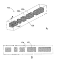
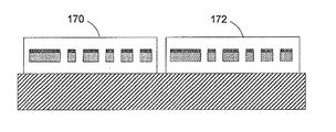
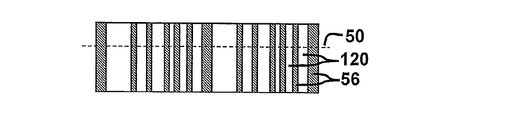
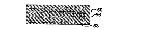
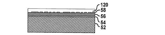
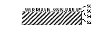
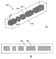
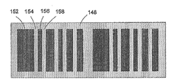
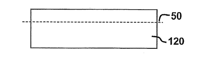
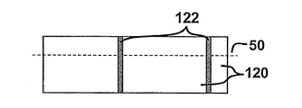
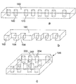
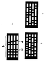
一例として、図1Aは、本発明のコード化されたマイクロ粒子を概略的に示す。マイクロ粒子100は、図面に示されるように、デカルト座標のY方向に沿って延長された直方体構造である。マイクロ粒子の長さに垂直な断面は、この例では正方形である、ほぼ同じ位相幾何学的形状を有する。
As an example, FIG. 1A schematically shows an encoded microparticle of the present invention. As shown in the drawing, the
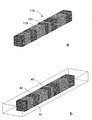
この特定の例におけるマイクロ粒子は、一組のセグメント(例えば、セグメント102)とセグメントの間に挟まれたギャップ(例えば、ギャップ104)を有する。具体的には、長さ(マイクロ粒子の長さに沿った、例えばY方向に沿った寸法)が異なるセグメントは、異なるコード化要素を表すが、ギャップは、好ましくは、マイクロ粒子の検出中にセグメントを区別するため、同じ長さを有する。この例におけるマイクロ粒子のセグメントは、マイクロ粒子内に、例えば本体106内に完全に封入される。代替の特徴として、セグメントは、セグメントの幾何学的中心が、細長いマイクロ粒子の幾何学的中心軸と整列するように配列することができる。セグメントとギャップの特定の列はコードを表す。コードは予め定められたコード体系から得られる。
The microparticles in this particular example have a set of segments (eg, segment 102) and a gap (eg, gap 104) sandwiched between the segments. Specifically, segments with different lengths (dimensions along the length of the microparticle, eg, along the Y direction) represent different coding elements, but the gap is preferably detected during detection of the microparticle. To distinguish the segments, they have the same length. The microparticle segments in this example are completely encapsulated within the microparticles, for example within the
マイクロ粒子のセグメントは任意の適切な懈怠が可能である。本発明の一例では、マイクロ粒子の各セグメントは、マイクロ粒子の長さに垂直に(すなわち、図1Aのデカルト座標のY方向に沿って)取った、ほぼ正方形の断面(すなわち、図1Aに示されるようなデカルト座標のX−Z面における断面)を有する。セグメントは、ほぼ正方形の断面を有するように製造されても、されなくてもよい。長方形、円形、楕円形、ソウ歯状、曲線状など、他の形状も適用可能である。特に、コード要素、すなわちセグメントとギャップは、他の任意の適切な所望の形状を取ることもできる。例えば、セグメント(及び/又はギャップ)はそれぞれ、長方形の断面(例えば、長方形のアスペクト比が2:1以上、例えば4:1以上、10:1以上、20:1以上、さらには100:1以上などであるが、好ましくは500:1未満である)を有してもよい。 The microparticle segments can be of any suitable fatigue. In one example of the present invention, each segment of microparticles is a substantially square cross section (ie, shown in FIG. 1A) taken perpendicular to the length of the microparticle (ie, along the Y direction of the Cartesian coordinate of FIG. 1A). In the XZ plane of Cartesian coordinates). The segments may or may not be manufactured to have a generally square cross section. Other shapes such as a rectangle, a circle, an ellipse, a sawtooth, and a curve are also applicable. In particular, the code elements, i.e. segments and gaps, may take any other suitable desired shape. For example, each segment (and / or gap) has a rectangular cross-section (eg, a rectangular aspect ratio of 2: 1 or higher, such as 4: 1 or higher, 10: 1 or higher, 20: 1 or higher, or even 100: 1 or higher. Etc., but preferably less than 500: 1).
図1Aのマイクロ粒子の例は、6つの主面を、すなわち、面(X=±x0、Y、Z)、面(X、Y、Z=±z0)、面(X、Y=±y0、Z)を有し、ここで、x0、y0、z0はそれぞれ、マイクロ粒子の幅、長さ、高さである。本発明によれば、上記の6つのうち少なくとも2つの面X=±x0(又は面Z=±z0)、より好ましくは、上記6つのうち少なくとも4つの主面X=±x0、面Z=±z0は、各面がへこみを有するか否かに関わらずほぼ連続している。この構成により、マイクロ粒子は、光学イメージング装置などの検出器に対してほぼ同じ幾何学的外観と特有性を示す。実際には、主面はほぼ平坦にすることができる。例えば、製造中に粗さ又は変化するプロファイルが生じたとしても、オーバー堆積やエッチング・バック技術、又は化学的機械的研磨(CMP)技術などの標準的な面加工技術、さらには平滑な垂直側壁プロファイルを作成するため、パターニング工程を適切に制御するなどの標準的な面加工技術を使用して、依然としてほぼ平坦な主面を得ることができる。 The example microparticle of FIG. 1A has six major surfaces: plane (X = ± x 0 , Y, Z), plane (X, Y, Z = ± z 0 ), plane (X, Y = ± y 0 , Z), where x 0 , y 0 , and z 0 are the width, length, and height of the microparticle, respectively. According to the present invention, at least two of the six surfaces X = ± x 0 (or surface Z = ± z 0 ), more preferably at least four of the six main surfaces X = ± x 0 , surfaces Z = ± z 0 is substantially continuous regardless of whether each surface has a dent or not. With this configuration, the microparticles exhibit approximately the same geometric appearance and uniqueness to detectors such as optical imaging devices. In practice, the main surface can be substantially flat. For example, standard surface processing techniques such as over-deposition, etch-back techniques, or chemical-mechanical polishing (CMP) techniques, and smooth vertical sidewalls, even if roughness or changing profiles occur during manufacturing To create a profile, standard surface processing techniques such as appropriate control of the patterning process can be used to obtain a substantially flat major surface.
コード要素、すなわちセグメントとギャップは、任意の所望の寸法を取ることができる。本発明の一例として、各コード化構造は、5μm(ミクロン)以下、例えば3ミクロン以下の、より好ましくは1ミクロン以下、例えば0.8又は0.5ミクロン以下の、特徴的な寸法を有する。特に、ギャップはほぼ同じ寸法に保たれるが、セグメントの寸法が変化する場合、各ギャップは、好ましくは、1.5ミクロン以下、例えば0.8又は0.5ミクロン以下の特徴的な寸法を有する。 The code elements, i.e. segments and gaps, can take any desired dimensions. As an example of the present invention, each encoded structure has a characteristic dimension of 5 microns or less, such as 3 microns or less, more preferably 1 micron or less, such as 0.8 or 0.5 microns. In particular, the gaps remain approximately the same size, but if the segment dimensions change, each gap preferably has a characteristic dimension of 1.5 microns or less, such as 0.8 or 0.5 microns or less. Have.
一例として、線幅が0.13の30.5cm(12インチ)のシリコン・ウェハ上にマイクロ粒子を形成する場合、ギャップ面積が0.13μmの最小幅を有し、透明度がより低いセグメントが(粒子の所望の長さ並びに、所望のコード化体系及びコードスペースに応じて)0.13μmからそれよりもはるかに大きな値までの幅を有するようにすることができる。使用されるウェハの製造に応じて、0.13〜1.85μm(例えば、0.25〜0.85μm)の最小ギャップ幅と最小セグメント幅が可能である。当然ながら、より大きな最小ギャップ長さとセグメント長さ(例えば、1.85〜5.0μm以上)も可能である。当然ながら、他のサイズのウェハ(10.2cm(4インチ)、15.2cm(6インチ)、20.3cm(8インチ)など)、シリコン以外(例えば、ガラス)のウェハ、さらにはシリコン以外の他の基板(例えば、大型のガラス・パネル)を使用することができる。 As an example, when forming microparticles on a 30.5 cm (12 inch) silicon wafer with a line width of 0.13, a segment with a minimum width of gap area of 0.13 μm and lower transparency ( Depending on the desired length of the particles and the desired coding scheme and code space, it can have a width from 0.13 μm to much larger values. Depending on the manufacture of the wafer used, a minimum gap width and a minimum segment width of 0.13 to 1.85 μm (eg, 0.25 to 0.85 μm) are possible. Of course, larger minimum gap lengths and segment lengths (eg, 1.85 to 5.0 μm or more) are possible. Of course, other size wafers (10.2 cm (4 inches), 15.2 cm (6 inches), 20.3 cm (8 inches), etc.), non-silicon (eg, glass) wafers, and other than silicon Other substrates (eg, large glass panels) can be used.
マイクロ粒子は、X方向、Y方向、及び/又はZ方向に同じ長さを有してもよいが、好ましくは、コード化されたマイクロ粒子は、2:1〜50:1、例えば4:1〜20:1の長さと幅の比を有する。本発明の一例では、マイクロ粒子の長さ(例えば、Y方向に沿った寸法)は、70ミクロン以下、50ミクロン以下、30ミクロン以下、例えば20ミクロン以下、16ミクロン以下、さらには10ミクロン以下である。マイクロ粒子の幅(例えば、X方向に沿った寸法)と、高さ(Z方向に沿った寸法)は、15ミクロン以下、10ミクロン以下、8ミクロン以下、4ミクロン以下、さらには1ミクロン以下、例えば0.13ミクロンであってもよい。0.5〜2ミクロン程度の小さな幅も可能である。図1Aに示し、かつ上述した形状以外に、マイクロ粒子は、ロッド、バー、ディスク、又は他の任意の所望の形状を取ってもよい。 The microparticles may have the same length in the X, Y, and / or Z directions, but preferably the encoded microparticles are 2: 1 to 50: 1, such as 4: 1. It has a length to width ratio of ˜20: 1. In one example of the present invention, the length of the microparticle (eg, dimension along the Y direction) is 70 microns or less, 50 microns or less, 30 microns or less, such as 20 microns or less, 16 microns or less, or even 10 microns or less. is there. The microparticle width (eg, dimension along the X direction) and height (dimension along the Z direction) are 15 microns or less, 10 microns or less, 8 microns or less, 4 microns or less, or even 1 micron or less, For example, it may be 0.13 microns. Small widths on the order of 0.5 to 2 microns are possible. In addition to the shapes shown in FIG. 1A and described above, the microparticles may take on a rod, bar, disk, or any other desired shape.
マイクロ粒子のコード化構造とギャップは、コード化構造とギャップが共に検出可能なコードを表す限り、任意の適切な形態を取ることができる。上述したように、マイクロ粒子の断面は、粒子の長さに垂直に取ったとき、正方形、長方形、円形、楕円形、あるいは、ソウ歯状若しくは曲線状又は他のプロファイルなどの任意の所望の形状である。断面が長方形のとき、長方形は、好ましくは、2:1以上、例えば4:1以上、10:1以上、20:1以上、さらには100:1以上であるが、好ましくは500:1未満であるアスペクト比(長さと幅又は高さの比)を有する。幅と高さの比は、1:1程度(正方形の断面)であるか、あるいは、1:4〜1:1の比、好ましくは、粒子が細長い側面のどこに存在するかに関わらず、マイクロ粒子のコードを検出することができるように、粒子が、粒子の幅又は高さを規定するいずれかの側面の上に存在することができる比を有することができる。 The microparticle coding structure and gap may take any suitable form, as long as both the coding structure and the gap represent a detectable code. As mentioned above, the cross-section of the microparticles, when taken perpendicular to the length of the particles, is square, rectangular, circular, elliptical, or any desired shape such as sawtooth or curvilinear or other profile It is. When the cross section is rectangular, the rectangle is preferably 2: 1 or more, such as 4: 1 or more, 10: 1 or more, 20: 1 or more, more preferably 100: 1 or more, but preferably less than 500: 1. It has a certain aspect ratio (ratio of length to width or height). The ratio of width to height is on the order of 1: 1 (square cross section), or a ratio of 1: 4 to 1: 1, preferably regardless of where the particles are on the elongated side. The particles can have a ratio that can be present on either side that defines the width or height of the particles so that the code of the particles can be detected.
コード化構造とギャップによって表されるコードの、迅速で、コスト効率が良く、信頼性が高く、かつ容易な検出を促進するため、各コード化構造は、検出手段に対して可能な限り全方向的であることが好ましい。すなわち、各コード化構造は、少なくとも二方向から、より好ましくはマイクロ粒子の長さに垂直な四方向(又は、断面が四辺形でない場合、全方向)から観察されたとき、ほぼ同じ幾何学的外観又は検出可能な特性を示す。したがって、コード化構造は、好ましくは、マイクロ粒子の長さに沿って、2回転対称性又は4回転対称性などの回転対称性を有する。 Each coding structure is as omnidirectional as possible with respect to the detection means in order to facilitate quick, cost-effective, reliable and easy detection of the code represented by the coding structure and the gap Preferably. That is, each coded structure has approximately the same geometrical shape when viewed from at least two directions, more preferably from four directions perpendicular to the length of the microparticle (or from all directions if the cross section is not quadrilateral). Appearance or detectable properties. Thus, the encoded structure preferably has a rotational symmetry, such as a two-fold symmetry or a four-fold symmetry, along the length of the microparticle.
本発明のマイクロ粒子は、粒子の形状又は長さ、及び所望のコードスペースに応じて、任意の適切な数のコード化構造を有することができる。具体的には、マイクロ粒子のコード化構造の総数は、1〜20個、より一般的には3〜15個、より一般的には3〜8個である。 The microparticles of the present invention can have any suitable number of coding structures depending on the shape or length of the particles and the desired code space. Specifically, the total number of microparticle coding structures is 1-20, more typically 3-15, more typically 3-8.
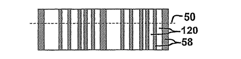
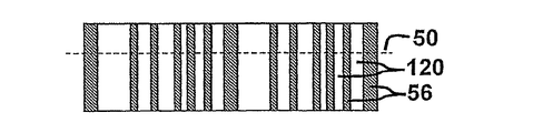
所望のコードは、多数のやり方でマイクロ粒子に組み込むか、又はマイクロ粒子によって表すことができる。一例として、予め定められたコード体系のコード化要素は、セグメント(1つ又は複数)によって表すことができ、例えば、長さが異なるセグメントはコード体系の異なるコード化要素を表す。異なる(又は同じ)長さを有し、ギャップが間に挟まれたセグメントの異なる空間的配列は、異なるコードを表す。このコードの組み込み方法では、間に挟まれるギャップは、好ましくは、特にセグメントが整列する方向の長さについて、ほぼ同じ寸法を有する。別の例として、コードは、長さが変化するギャップを配列することによってマイクロ粒子に組み込まれ、セグメントはほぼ同じ寸法を有し、隣接したギャップ間に配置される。別の例では、セグメントとギャップは両方とも、コードを表すため、その寸法が変化する。実際に、コードは、セグメント、ギャップ、及びそれらの組み合わせを使用して、他の多くの代替的方法で表すこともできる。 The desired code can be incorporated into or represented by the microparticle in a number of ways. As an example, coding elements of a predetermined coding scheme can be represented by segment (s), for example, segments of different lengths represent coding elements of different coding schemes. Different spatial arrangements of segments having different (or the same) lengths with gaps in between represent different codes. In this cord integration method, the gaps sandwiched between them preferably have approximately the same dimensions, particularly with respect to the length in the direction in which the segments are aligned. As another example, the code is incorporated into the microparticle by arranging gaps of varying length, and the segments have approximately the same dimensions and are placed between adjacent gaps. In another example, both the segment and the gap represent a code, so their dimensions change. Indeed, the code can also be expressed in many other alternative ways using segments, gaps, and combinations thereof.
予め定められたコード体系から得られるコードを表すため、セグメントとギャップは、細長いマイクロ粒子の長さ(Y方向)に沿って配列される(ただし、二次元、又はさらには三次元の配列も可能である)。具体的には、セグメントとギャップは長さに沿って交互に整列され、各セグメントは隣接したギャップによって分離され(恐らくは、完全に分離され隔離される)、各ギャップは隣接したセグメントによって分離される(恐らくは、完全に分離され隔離される)。このことは、以下に考察される図1Bの断面図により良好に示されている。 Segments and gaps are arranged along the length (in the Y direction) of elongated microparticles (representing two-dimensional or even three-dimensional arrangements) to represent codes derived from a predetermined coding scheme Is). Specifically, segments and gaps are alternately aligned along the length, each segment is separated by an adjacent gap (perhaps completely separated and isolated), and each gap is separated by an adjacent segment (Maybe completely separated and isolated). This is better illustrated by the cross-sectional view of FIG. 1B discussed below.
本発明の一例では、任意の適切な数のセグメントを使用することができ、例えば、透明度がより低い材料(セグメント間に挟まれたギャップに比べて)の、2〜20個、より一般的には3〜15個のセグメント(より一般的には3〜8個のセグメント)が、コード化されたマイクロ粒子内に設けられる。コードを形成するため、透明度がより低い材料のセグメントの長さを変えることが可能である。あるいは、透明度がより低い材料のセグメントはそれぞれ、ほぼ同じ長さを有するが、透明度がより高い材料の中間セグメントは変化する長さを有することができる。当然ながら、コードを表すため、透明度がより高い材料のセグメントと透明度がより低い材料の中間セグメントが両方ともその長さが変化しても良い。 In one example of the present invention, any suitable number of segments can be used, such as 2-20, more generally, of a less transparent material (as compared to a gap sandwiched between segments). 3-15 segments (more typically 3-8 segments) are provided within the encoded microparticle. It is possible to vary the length of the segments of the less transparent material to form the cord. Alternatively, each segment of the less transparent material may have approximately the same length, while the middle segment of the more transparent material may have a varying length. Of course, to represent a code, the length of both the more transparent material segment and the less transparent material intermediate segment may vary in length.
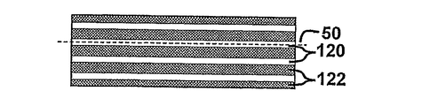
図1Bを参照すると、断面は、図1Aの粒子のY−Z面で(又は同等にX−Y面で)で取られている。セグメント(例えば、セグメント102)とギャップ(例えば、ギャップ104)は、マイクロ粒子の長さに沿って交互になっている。 Referring to FIG. 1B, the cross section is taken in the YZ plane (or equivalently in the XY plane) of the particle of FIG. 1A. Segments (eg, segment 102) and gaps (eg, gap 104) alternate along the length of the microparticle.
マイクロ粒子に組み込まれたコードを検出できるようにするため、各マイクロ粒子内のセグメントとギャップは、光学特性、電気特性、磁性特性、流体力学特性、又は、所望の検出方法に適合した他の所望の特性が異なる材料から成ることができる。一例では、セグメントとギャップは、可視スペクトル内の透過光及び/又は反射光のもとで、直接空間的に区別することができる。例えば、コード検出が光学イメージングに依存するとき、区別可能な特性(セグメント対ギャップ)は、画像化に使用される特定の光(任意の所望の電磁放射、例えば、可視光と近可視光、IR、紫外光など)に対する透過率の差である。セグメントは、間に挟まれる間隔材料よりも光吸収性(又は光反射性)にする(あるいは、その逆にする)ことができる。コード検出が電気特性の測定に依存するとき、特性は、抵抗とコンダクタンスである。コード検出が磁気による方法を伴うとき、特性は、インダクタンスと電気インダクタンスである。コード検出が流動力学的方法を伴うとき、特性は、コード検出に使用される特定の流体に対する粘性である。どの特定の特性に依存するかに関わらず、セグメントとギャップは、対応するコード検出方法を使用して差異を検出することができるように、特定の特性において十分な差異を示すことが好ましい。特に、光学イメージングを用いてコードが検出されるとき、セグメントとギャップは、マイクロ粒子の画像化に使用される特定の光に対して、異なる透過率(光透過モードの場合)又は反射率(光反射モードの場合)を示す材料から成る。例えば、透明度がより低い材料のマイクロ粒子のセグメントは、その上に入射する可視光又は近可視光の30%以上、好ましくは50%以上、又は例えば80%以上を阻止かつ/又は反射することができる。 In order to be able to detect the code embedded in the microparticle, the segments and gaps within each microparticle can be optical, electrical, magnetic, hydrodynamic, or other desired, adapted to the desired detection method. Can be made of different materials. In one example, segments and gaps can be directly spatially distinguished under transmitted and / or reflected light in the visible spectrum. For example, when code detection relies on optical imaging, the distinguishable property (segment vs. gap) is the specific light used for imaging (any desired electromagnetic radiation, eg, visible and near visible light, IR , Ultraviolet light, etc.). The segments can be more light absorptive (or light reflective) than the intervening spacing material (or vice versa). When code detection relies on measuring electrical properties, the properties are resistance and conductance. When code detection involves a magnetic method, the characteristics are inductance and electrical inductance. When code detection involves a rheological method, the characteristic is the viscosity for the particular fluid used for code detection. Regardless of which specific characteristic depends on, it is preferred that the segments and gaps show sufficient differences in the specific characteristic so that the corresponding code detection method can be used to detect the difference. In particular, when the code is detected using optical imaging, the segments and gaps have different transmission (in the case of light transmission mode) or reflectance (light) for the specific light used for microparticle imaging. (In the reflection mode). For example, a segment of microparticles of a less transparent material may block and / or reflect 30% or more, preferably 50% or more, or such as 80% or more of the visible or near visible light incident thereon. it can.
物体による電磁放射の透過率は物体の厚さに応じて変わるという事実を鑑みて、検出光の30%以上、好ましくは50%以上、又は例えば80%以上(あるいは、さらには90%以上)を阻止かつ/又は反射することができるセグメントが好ましいが、コード化構造の間のギャップは、検出光の50%以上、70%以上、80%以上、又はさらには90%以上を透過することができる材料から、かつそのような寸法で得られる。あるいは、セグメントとギャップは、透過率の差異の比がコードγを検出するのに十分であるように、例えば、5%以上、10%以上、20%以上、50%以上、70%以上であるように、異なる材料から成る。透過率は、通過した光と入射光の光度の比として決められる。 In view of the fact that the transmittance of electromagnetic radiation by the object varies depending on the thickness of the object, 30% or more of the detection light, preferably 50% or more, or for example 80% or more (or even 90% or more). Segments that can block and / or reflect are preferred, but the gap between the coding structures can transmit more than 50%, more than 70%, more than 80%, or even more than 90% of the detected light. From the material and with such dimensions. Alternatively, the segment and the gap are, for example, 5% or more, 10% or more, 20% or more, 50% or more, 70% or more so that the ratio of the transmittance difference is sufficient to detect the code γ. As such, it consists of different materials. The transmittance is determined as the ratio of the light intensity of the light passing through and the incident light.
微細構造は、有機材料及び/又は無機材料、あるいは有機・無機材料の混合物で作成することができる。具体的には、ギャップ(好ましくは、可視光又は近可視光に対する透過性がより高い)とセグメント(好ましくは、ギャップに比べて、可視光又は近可視光に対する透過性がより低い)はそれぞれ、有機材料又は無機材料、あるいは混合有機・無機材料から成ることができる。セグメントは、金属(例えば、アルミニウム)、前周期遷移金属(例えば、タングステン、クロム、チタン、タンタル、又はモリブデン)、又はメタロイド(例えば、シリコン又はゲルマニウム)、あるいはそれらの組み合わせ(又は、窒化物、酸化物、及び/若しくは炭化物)から成ることができる。特に、セグメントは、メタロイド若しくは前周期遷移金属の酸化物、メタロイド若しくは前周期遷移金属の窒化物、又はメタロイド若しくは前周期遷移金属の炭化物を含む化合物など、セラミック化合物から成ることができる。前周期遷移金属は、周期表の3b族(Sc、Y、Lu、Lr)、4b族(Ti、Zr、Hf、Rf)、5b族(V、Nb、Ta、Db)、6b族(Cr、Mo、W、Sg)及び7b族(Mn、Tc、Re、Bh)に基づくものである。しかし、4b〜6b族の前周期遷移金属、特に、タングステン、チタン、ジルコニウム、ハフニウム、ニオブ、タンタル、バナジウム、クロムが好ましい。 The microstructure can be made of organic materials and / or inorganic materials, or a mixture of organic and inorganic materials. Specifically, the gap (preferably more transmissive to visible or near visible light) and the segment (preferably less transmissive to visible or near visible light compared to the gap), respectively, It can consist of organic or inorganic materials, or mixed organic / inorganic materials. The segment can be a metal (eg, aluminum), a transition metal (eg, tungsten, chromium, titanium, tantalum, or molybdenum), or a metalloid (eg, silicon or germanium), or a combination (or nitride, oxide) And / or carbide). In particular, the segment may be composed of a ceramic compound, such as a metalloid or an oxide of a transition metal, a nitride of a metalloid or a transition metal, or a compound containing a metalloid or a transition metal carbide. The periodic transition metals are group 3b (Sc, Y, Lu, Lr), group 4b (Ti, Zr, Hf, Rf), group 5b (V, Nb, Ta, Db), group 6b (Cr, Mo, W, Sg) and 7b group (Mn, Tc, Re, Bh). However, the 4b-6b group transition metal, particularly tungsten, titanium, zirconium, hafnium, niobium, tantalum, vanadium, and chromium are preferred.
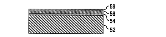
この例では透明度がより高いギャップは、セグメントよりも透明度が高い任意の適切な材料を含むことができる。混合材料が選択される場合、間隔材料は、特に、シロキサン材料又はシルセスキオキサン材料などである。間隔材料は、無機材料の場合、ガラス材料などである。ボロン又はリンのドープ剤/合金化剤を有するか、又は有さない、薄膜状に堆積された二酸化シリコンが適切な材料である。例えば、窒化シリコン、窒化酸化シリコン、酸化ゲルマニウム、窒化酸化ゲルマニウム、シリコン・ゲルマニウム窒化酸化物、又は様々な遷移金属酸化物など、他の無機ガラス材料も適切である。塗布ガラス(SOG)を使用することもできる。有機材料がギャップ材料に使用される場合、プラスチック(例えば、ポリスチレン又はラテックス)を使用することができる。 In this example, the higher transparency gap can include any suitable material that is more transparent than the segment. When a mixed material is selected, the spacing material is in particular a siloxane material or a silsesquioxane material. In the case of an inorganic material, the spacing material is a glass material or the like. Thin film deposited silicon dioxide with or without boron or phosphorus dopant / alloying agent is a suitable material. Other inorganic glass materials are also suitable, such as silicon nitride, silicon nitride oxide, germanium oxide, germanium nitride oxide, silicon germanium nitride oxide, or various transition metal oxides. Coated glass (SOG) can also be used. If an organic material is used for the gap material, a plastic (eg, polystyrene or latex) can be used.
セグメントとギャップは両方とも、CVD(化学堆積法)、PVD(物理堆積法)、塗布、ゾル・ゲルなどの任意の適切な方法によって堆積させることができる。CVD堆積法が使用される場合、CVDは、LPCVD(低圧化学堆積法)、PECVD(プラズマ促進化学堆積法)、APCVD(大気圧化学堆積法)、SACVD(減圧化学堆積法)などである。PVD法が使用される場合、所望の最終材料に応じて、スパッタリング又は反応スパッタリングが可能である。塗布材料(SOG又は混合有機・無機シロキサン材料。 Both segments and gaps can be deposited by any suitable method such as CVD (Chemical Deposition), PVD (Physical Deposition), Application, Sol or Gel. When CVD deposition is used, the CVD is LPCVD (low pressure chemical deposition), PECVD (plasma enhanced chemical deposition), APCVD (atmospheric pressure chemical deposition), SACVD (low pressure chemical deposition). If a PVD method is used, sputtering or reactive sputtering is possible depending on the desired final material. Coating material (SOG or mixed organic / inorganic siloxane material.
より具体的な例として、セグメントは、CVD(化学堆積法)によって堆積させた非晶質シリコンなどの、任意の適切なシリコン材料から成ることができる。ポリシリコン又は単結晶シリコンも、上述したような広範囲の他の材料と同様に適切である。必須ではないが、セグメントのために選択される材料は、堆積厚さが高度に制御され、面粗さが低く、パターニングとリリースの両方におけるエッチングが高度に制御され(例えば、パターニングにはドライ・プラズマ・エッチングを、リリースには湿式又は乾式化学エッチングを使用する)、かつCMOSプロセスの適合性が高いことが好ましい。ギャップ材料は、CVD堆積された二酸化シリコンでよい。二酸化シリコンは、リン又はボロンなどの、ドーピング/合金化材料を包含してもよい。セグメントとギャップに対して、透明度のより高い材料とより低い材料の組み合わせを選択する際、温度が考慮に入れられてもよい。 As a more specific example, the segments can be composed of any suitable silicon material, such as amorphous silicon deposited by CVD (Chemical Deposition). Polysilicon or single crystal silicon is suitable as well as a wide range of other materials as described above. Although not required, the materials selected for the segments are highly controlled in deposition thickness, low in surface roughness, and highly controlled in both patterning and release (e.g., dry patterning for patterning). Preferably, plasma etching is used (wet or dry chemical etching is used for release) and the CMOS process is highly compatible. The gap material may be CVD deposited silicon dioxide. Silicon dioxide may include doping / alloying materials such as phosphorus or boron. Temperature may be taken into account when selecting a combination of higher and lower transparency materials for the segments and gaps.
図2は、本発明の別の例のコード化されたマイクロ粒子を概略的に示す。粒子19は長方形の断面を有し、ほぼ平坦な形状である。例えば、マイクロ粒子の高さと幅の比は、任意の所望の比であり、例えば、1:1.2〜1:4以上などであることができる。
FIG. 2 schematically illustrates another example encoded microparticle of the present invention. The
図3aは、本発明の別の例のコード化されたマイクロ粒子を概略的に示す。図3aを参照すると、マイクロ粒子116は第1の材料118と第2の材料120から成る。2つの材料は、化学的に異なるか、あるいは、同じ化学組成であり、ただしグレイン構造又は厚さなどの他の観点においては異なる。2つの材料は、所望の検出スキームを用いて区別することができる。この例では、材料はそれぞれ、好ましくは、粒子の断面を完全に横断する。この構造を作成する一例のプロセスは、本明細書で以下に開示するパターニングとエッチング方法の変形例、及び/又は高エネルギー・イオン注入法など、IC/MEMS(集積回路/微小電子機械システム)分野からのものを包含する、上述したような製造方法を伴う。
FIG. 3a schematically illustrates another example encoded microparticle of the present invention. Referring to FIG. 3 a, the
図3bは、本発明の別の例のコード化されたマイクロ粒子を概略的に示す。図3bを参照すると、マイクロ粒子は、第3の材料44に取り囲まれた、2つの異なる材料40、42の交互になったセグメントから成り、それにより、交互になったセグメントのパターンが検出可能なコードを形成する。他の例のマイクロ粒子は、粒子の内部に2つを超える異なる材料を含有してもよい。粒子は、任意の適切な断面形状を有してもよく、図示される例では細長いものである。
FIG. 3b schematically shows another example encoded microparticle of the present invention. Referring to FIG. 3b, the microparticle consists of alternating segments of two
上述の例では、マイクロ粒子は、区別可能な光学特性など、選択された区別可能な特性の材料から成る。上述の例では、一方の材料は他方の材料よりも大きな透明度又は光透過率を有し、その差異は拡大することによって検出可能である。上述の特定の例は、一方の材料が光吸収性材料であり、他方の材料が、可視スペクトルにおいてより大きな光透過性を有する半透明又は透明材料である(あるいは、例えば、UV、IRなどの別のスペクトルでは、異なる検出システムが使用されるべきである)。別の例では、一方の材料は光反射性材料であり、他方の材料は、光吸収性又は光透過性のどちらかである。一方の材料の不透明度がより高く、他方の材料の不透明度がより低い場合の、あるいは一方の材料の反射性がより高く、他方の材料の反射性がより低い場合の検出可能な差異は、この例の範囲内である。上述したように、不透明材料と透明材料の交互になった部分は、他の材料の中でも特に、シリコンとガラスで作成することができる。ほぼ全ての材料の透過率(及び反射率)が材料の厚さに依存するという事実に鑑みて、マイクロ粒子は、コード化構造(すなわち、コードのコード化要素を表す構造)が単一の材料から得られるようにして形成されてもよい。図4a、図4bは、そのコード化構造がシリコンなどの単一の材料から得られる、代表的なマイクロ粒子を概略的に示す。 In the example described above, the microparticles are comprised of a material with selected distinguishable properties, such as distinguishable optical properties. In the above example, one material has a greater transparency or light transmission than the other, and the difference can be detected by magnification. In the specific example described above, one material is a light absorbing material and the other material is a translucent or transparent material with greater light transmission in the visible spectrum (or, for example, UV, IR, etc. In another spectrum, a different detection system should be used). In another example, one material is a light reflective material and the other material is either light absorbing or light transmissive. The detectable difference when the opacity of one material is higher and the other material is lower, or when one material is more reflective and the other material is less reflective, Within the scope of this example. As described above, alternating portions of opaque and transparent materials can be made of silicon and glass, among other materials. In view of the fact that the transmissivity (and reflectivity) of almost all materials depends on the thickness of the material, microparticles have a single coded structure (ie, a structure representing the coded elements of the code). May be formed as follows. Figures 4a and 4b schematically show representative microparticles whose coding structure is obtained from a single material such as silicon.
図4aを参照すると、代表的なマイクロ粒子の断面図が示されている。マイクロ粒子206は、一組のコード化構造(例えば210、212、208、214)を含み、それらの組み合わせは、コード体系から得られるコードを表す。コードを組み込むため、コード化構造は幅などの異なるプロファイルを有し、異なる幅を備えた異なる構造が特定の位置に位置付けられる。コード化構造を決め、かつ後でコード検出を行うため、透過率しきい値厚さ(それ以下になると、材料が可視光と近可視光などの特定の光に対して可視であるようなしきい値)未満の厚さを備えた一組のギャップ(例えば、ギャップ212、214)。図1aに示される例とは異なり、コード化構造は完全には分離又は隔離されていない。マイクロ粒子に組み込まれたコードは、例えば、コード化構造間の隣接したギャップ(例えば、212、214)よりも透過率が低い、コード化構造(例えば、210、208)の異なる透過率に基づいて、読み取ることができる。
Referring to FIG. 4a, a cross-sectional view of a representative microparticle is shown. The
生体分子試料がマイクロ粒子の面に付着されることになる、マイクロ粒子の利用、特に生物学/生化学/生物医学/生物工学における利用を促進するため、固定化層が微細構造の面を被覆するのが望ましいことがある。 The immobilization layer covers the surface of the microstructure in order to facilitate the use of microparticles, in particular in biology / biochemistry / biomedicine / biotechnology, where biomolecular samples will be attached to the surface of the microparticles It may be desirable to do so.
図4bは、図4aのマイクロ粒子の透過モード画像を概略的に示す。図4bを参照すると、暗い領域210、208はそれぞれ、図4aのコード化構造210、208に対応する。白い領域212、214はそれぞれ、図4aのコード化構造212、214に対応する。光透過率のより高い部分とより低い部分とに使用される材料が同じ場合であっても、依然として、透過率プロファイルによって検出可能なコードが可能になる。図4のようなマイクロ粒子は、別の材料(例えば、二酸化シリコン)の最下層を備え、所望に応じて別の材料(例えば、二酸化シリコン)の第2の層で被覆させる。そのようなマイクロ粒子は、図1aの構造とほぼ同じ直方体形状を有するように、材料(例えば、二酸化シリコン)で完全に包むこともできる。図4cは、本発明の別の例のコード化されたマイクロ粒子を概略的に示す。図4cを参照すると、マイクロ粒子は、より狭い領域によって接続されたより大きな領域を含む。マイクロ粒子は、コードが検出可能であるように、材料によって取り囲まれる。
FIG. 4b schematically shows a transmission mode image of the microparticles of FIG. 4a. Referring to FIG. 4b, the
図4a、図4cのマイクロ粒子は、多くの方法で製造することができ、その1つが、図4dの代表的な製造中のマイクロ粒子の断面図に概略的に示される。図4dを参照すると、特定の光(例えば、可視光又は近可視光)に対して透過性の材料(例えば、ガラス、石英、又は他の適切な材料)から成る基板216が用いられる。分離層217が基板216上に堆積される。分離層は、エッチング又は他の適切な方法によって、後でマイクロ粒子をガラス基板から切離すために設けられる。エッチングは、湿式、乾式、又はプラズマ・エッチングで、したがって、分離層は、本明細書において上述したような、選択されたエッチング方法を用いてエッチング可能な材料から成ることが望ましい。粒子構造の上述の実施形態に関して記載したように、粒子が基板上に直接形成され、続いて基板にバルク・エッチングを施すことによってリリースされるように、分離層は省略されてもよい。
The microparticles of FIGS. 4a, 4c can be produced in a number of ways, one of which is schematically illustrated in the cross-sectional view of the representative microparticle in production of FIG. 4d. Referring to FIG. 4d, a
コード化構造層は、構造218、222、220などのコード化構造を形成するように、堆積されパターニングされる。コード化構造を形成した後、形成されたコード化構造上に包囲層224が堆積される。包囲層は、アッセイの際に標的試料に対して露出されるので、層224は、マイクロ粒子がその中に分配されるべきアッセイ溶液中の化学成分に対する耐性を持つ材料から成ることが望ましい。さらに、核酸(例えば、DNA又はRNA)、タンパク質、抗体、酵素、薬剤、受容体、配位子、又は層の面上の分子などのプローブ分子を保持するため、層224はプローブ分子を不動化できることが望ましい。
The encoded structure layer is deposited and patterned to form an encoded structure such as
以下の代表的な製造プロセスは、セグメントとギャップを備えたマイクロ粒子を参照して考察されるが、以下の方法は、他の多くのタイプのコード要素に適用可能であることに留意されたい。 Although the following exemplary manufacturing process is discussed with reference to microparticles with segments and gaps, it should be noted that the following methods are applicable to many other types of code elements.
本発明の微細構造は、MEMS製造方法などの微細加工の広範な分野内にある方法を用いて製造することができる。MEMSは、多種多様な用途向けのマイクロスケール構造を形成するため、半導体産業の技術を使用する。MEMS技術は、全ての状況においてではないものの、一般的には、薄膜の堆積、乾式及び/又は湿式方法を用いたエッチングと、パターン形成のためのリソグラフィを含む。MEMSは半導体産業から派生したものなので、コスト効率が良く、大量の、かつ精密な生産のための、莫大な世界規模の製造基盤が整っている。一般的に言えば、MEMSプロセス全体が既存の集積回路プロセスに類似しているほど、例えばCMOSに適合しているほど、この基盤がより使用しやすい。 The microstructure of the present invention can be manufactured using methods within a broad field of microfabrication, such as MEMS manufacturing methods. MEMS uses technology from the semiconductor industry to form microscale structures for a wide variety of applications. MEMS technology, although not in all situations, generally involves thin film deposition, etching using dry and / or wet methods, and lithography for patterning. Since MEMS is derived from the semiconductor industry, it has a vast global manufacturing base for cost-effective, high volume and precise production. Generally speaking, the more similar the entire MEMS process is to the existing integrated circuit process, for example, the more compatible it is with CMOS, the easier it is to use this substrate.
本発明の微細構造は、集積回路(例えば、相互接続)又はMEMSに使用される製造方法など、多くの方法で製造することができる。以下では、マイクロ粒子を作成するためのMEMS製造と適合性がある代表的な製造方法が、図5及び図6a〜図6mを参照して考察されるが、その際、マイクロ粒子は、非晶質シリコンから成る不透明なセグメントと、二酸化シリコンから成る可視光透過性のギャップとを含む。以下の製造の考察は、単に実証のためのものに過ぎず、本発明の範囲を限定するものと解釈されるべきではないことが、当業者には理解されるであろう。実際に、本発明の趣旨から逸脱することなく、多くの製造方法を使用することができる。 The microstructures of the present invention can be manufactured in many ways, such as those used in integrated circuits (eg, interconnects) or MEMS. In the following, representative manufacturing methods that are compatible with MEMS manufacturing to make microparticles will be discussed with reference to FIGS. 5 and 6a-6m, where the microparticles are amorphous. It includes an opaque segment made of quality silicon and a visible light transmissive gap made of silicon dioxide. It will be appreciated by those skilled in the art that the following manufacturing considerations are merely for demonstration purposes and should not be construed as limiting the scope of the invention. Indeed, many manufacturing methods can be used without departing from the spirit of the present invention.
図5を参照すると、工程122でシリコン基板が用意される。(本明細書においてさらに後述されるように)ガラス・ウェハ又はガラス・パネルなどの他の基板を使用することもできる。シリコン基板と仮定すると、工程124で基板上に二酸化シリコン層を堆積する。堆積は、上述したように、CVD、PVD、塗布など、多くの適切な薄膜堆積技術を用いて行うことができる。次に、工程126で非晶質シリコン層がSiO2層上に堆積され、続いて、工程128でハード・マスク酸化物層が堆積される。必須ではないが、ハード・マスクを使用することによって、特に非晶質シリコン層が比較的厚い(例えば、1μm以上の厚さ)とき、トポロジーによって引き起こされるフォトレジスト・コーティングの問題が軽減される。次に、工程130でハード・マスク酸化物層がパターニングされる。パターニングされたハード・マスク層を用いて、工程132で、所望のパターンを形成するように、プラズマ・エッチングによって非晶質シリコン層にエッチングが施される。次に、工程134でSiO2の最上層がパターニングされたシリコン層上に堆積され、続いて、工程136で二酸化シリコン層がパターニングされて、個別の(ただしまだリリースされていない)マイクロ粒子が形成される。次に、シリコン基板をエッチングし、マイクロ粒子を個々の粒子として分離させる無指向性シリコン・エッチングによって、工程140でマイクロ粒子がシリコン基板からリリースされる。上述したような図5のフローチャートは、異なる工程におけるマイクロ粒子の断面図と平面図においてより良好に示される。断面図及び平面図は図6a〜図6mに概略的に示される。
Referring to FIG. 5, a silicon substrate is prepared at
図6aを参照すると、SiO2層146、シリコン層148、ハード・マスク層150が、シリコン基板142上に順次堆積される。次に、ハード・マスク層150は、図6bに示されるように、セグメント片(例えば、152及び156)とギャップ片(例えば、154、158)を形成するようにパターニングされる。ハード・マスク層をパターニングすることによって形成されたセグメント片とギャップ片は、標的のマイクロ粒子のセグメントとギャップに対応する。セグメント片とギャップ片は、図6cのマイクロ粒子の平面図により良好に示される。図6cを参照すると、セグメント片(例えば、152、156)とギャップ片(例えば、154及び158)は、層148が上面から見えるように形成される。
Referring to FIG. 6a, a SiO 2 layer 146, a
層のパターニングは多くの方法で行うことができ、その1つは、半導体集積回路やMEMSデバイスの標準的な製造に広く使用されるフォトリソグラフィである。MEMS産業に使用されるフォトリソグラフィの最も一般的な形態は、接触フォトリソグラフィである。レチクル(マスクとして知られる)は、一般的に、ガラス・プレート上の二進クロム・パターンから成る。レチクルは、フォトレジストで覆われたウェハ(又は他の基板)に非常に近接して、又はそれと接触して置かれる。UV光がマスクを通して照射されて、フォトレジストを露光する。次に、ウェハが現像されて、露光領域内のフォトレジストが除去される(ポジティブ型のフォトレジストの場合)。結果として、レチクル上のパターンがフォトレジストに転写され、それが後に続くエッチング工程のマスクの役割を果たす。 Layer patterning can be done in many ways, one of which is photolithography widely used in standard manufacturing of semiconductor integrated circuits and MEMS devices. The most common form of photolithography used in the MEMS industry is contact photolithography. A reticle (known as a mask) typically consists of a binary chrome pattern on a glass plate. The reticle is placed in close proximity to or in contact with a wafer (or other substrate) covered with photoresist. UV light is irradiated through the mask to expose the photoresist. Next, the wafer is developed to remove the photoresist in the exposed area (in the case of a positive type photoresist). As a result, the pattern on the reticle is transferred to the photoresist, which serves as a mask for the subsequent etching process.
投影フォトリソグラフィは、最新の集積回路製造にのみ使用される別のタイプのフォトリソグラフィである。マスクを物理的に接触させる代わりに、投影フォトリソグラフィは、ウェハ上にマスク・パターンの焦点を合わせるためのレンズ系を使用する。このシステムの主要な利点は、投影光学系によってマスク・パターンを収縮できることである。代表的なシステムは5倍の縮小係数を有する。一般に、投影を用いて、接触リソグラフィに比べてはるかに小さな形体サイズを印刷することができる。投影フォトリソグラフィ・システムは、ステップ・アンド・リピート・システム(又は、略してステッパ)としても知られている。マスク上の最大のパターン又はフィールドのサイズは、ウェハ直径よりも大幅に小さい。マスク・パターンは、ウェハ上で繰り返し露光(「順送り」)されて、「ダイ」のアレイを形成する。順送りの距離は、ウェハ・ステージが露光の間にX方向とY方向に移動する距離であり、通常はダイのサイズに等しい。この代表的なスキームにより、同一のダイの重なり合わないアレイが作成されて、その後に、ウェハ上のダイを並列処理することが可能になる。 Projection photolithography is another type of photolithography that is used only in modern integrated circuit manufacturing. Instead of physically contacting the mask, projection photolithography uses a lens system to focus the mask pattern on the wafer. The main advantage of this system is that the mask pattern can be contracted by the projection optics. A typical system has a reduction factor of 5 times. In general, projection can be used to print feature sizes that are much smaller compared to contact lithography. Projection photolithography systems are also known as step-and-repeat systems (or steppers for short). The largest pattern or field size on the mask is much smaller than the wafer diameter. The mask pattern is repeatedly exposed ("forwarded") on the wafer to form an array of "dies". The forward feed distance is the distance that the wafer stage moves in the X and Y directions during exposure and is usually equal to the die size. This exemplary scheme creates a non-overlapping array of identical dies, after which the dies on the wafer can be processed in parallel.
ハード・マスク層(150)は、図6d及び図6eに示されるような離散的な区域を形成するため、さらにパターニングされる。図6dに示されるように、ハード・マスク層150は、離散的なハード・マスク区域(例えば、図6eの区域160、162、164、166)を形成するように、X方向とY方向にパターニングされる。次に、これらの離散的なハード・マスク区域は、下の層に離散的なシリコン区域を形成するために使用される。
The hard mask layer (150) is further patterned to form discrete areas as shown in FIGS. 6d and 6e. As shown in FIG. 6d, the
上述の例では、ハード・マスク層のパターニングは2つの個別のリソグラフィ工程で行われる。代替例では、レチクルはパターンを含んでもよいので、ハード・マスクのパターニングは単一のリソグラフィ工程を用いて実施することができる。さらなる代替例として、ハード・マスクは省略することができ、二工程又は単一工程どちらかのリソグラフィ・プロセスが使用される。 In the above example, the patterning of the hard mask layer is performed in two separate lithographic steps. In the alternative, the reticle may include a pattern, so that the patterning of the hard mask can be performed using a single lithographic process. As a further alternative, the hard mask can be omitted and either a two-step or single-step lithography process is used.
ハード・マスク最上層をパターニングした後、透明度がより高い材料の区域(例えば、図6fに示されるようなギャップ区域170、174)を間に有して、シリコン・セグメント168、172などの対応する離散的なシリコン区域を基板上に形成するように、シリコン層148にエッチングが施される。図6fに示されるマイクロ粒子の平面図が、図6gに概略的に示される。図6gに見られるように、ここで、上から見たときに透過層146が露出しており、セグメント160、162、164、166が透過層146上に形成されている。製造プロセスのこの時点における構造のSEM画像が図9a、図9bに示される。構造は、非常に高い精度、例えば垂直な側壁と明確な角を有する。当然ながら、より丸みを帯びた構造もこれらの方法の範囲内にある。
After patterning the hard mask top layer, corresponding areas such as
シリコン層148をパターニングした後、次に、図6hに示されるように透過層168が堆積される。光透過性がより高い層168は、光透過性がより高い層146と同じ材料から成っていてもいなくてもよい。図6hのマイクロ粒子の平面図が図6iに概略的に示される。基板上の粒子の斜視図が図8に示される。
After patterning the
次に、マイクロ粒子は互いから分離されるが、図6jに示されるように、下にある基板に付着されたままである。図6kは、図6jのマイクロ粒子の平面図を概略的に示し、図中、各マイクロ粒子は隣接したマイクロ粒子からは分離されているが、光透過層(すなわち、図6hの層168)によって取り囲まれている。最後に、図6lの断面図に示されるように、分離されたマイクロ粒子はシリコン基板142から切り離される。シリコン基板から切り離されたマイクロ粒子の平面図が図6mに示される。下にある基板からのマイクロ粒子の切り離し(「リリース」工程)は、任意の適切なエッチング剤を用いて、好ましくは、全方向でエッチングを施し、マイクロ粒子をアンダーカットするのに適合したガス又は液体を用いて行うことができる。基板自体をエッチングする代わりに、追加の犠牲層を基板上に設けることができる。エッチングは、湿式、乾式、又はプラズマ・エッチングなどであり、したがって、分離層は、選択されたエッチング方法を用いてエッチングを施すことが可能な材料から成ることが望ましい。特に、エッチング剤は、ハロゲン間化合物(例えば、BrF3又はBrCl3)、希ガスハロゲン化物(例えば、XeF2)、又はHFなどの酸性蒸気など、自発性気相化学エッチング剤である。TMAH、KOH(又は、NaOH、CeOH、RbOH、NH4OHなどの他の水酸化物)、EDP(エチレン・ジアミン・ピロカテコール)、アミン没食子酸塩、HNA(フッ化水素酸+硝酸+酢酸)が作用しないようにしてガラスをエッチングする−HF、又は他の任意の適切なシリコン・エッチング剤(リリースの際に除去すべき基板又は層がシリコン(非晶質シリコン若しくはポリシリコン若しくは単結晶シリコン)、又はタングステン、窒化タングステン、モリブデン、チタン、あるいはXeF2などのシリコン・エッチング剤中で除去できる他の材料のとき)などの液体を使用して、マイクロ粒子をリリースすることもできる。除去されるべき材料がシリコンではない場合、エッチング剤は、当然ながら、犠牲材料に適合される(例えば、フォトレジスト又はポリイミド犠牲層などのための酸素プラズマ分離)。
The microparticles are then separated from each other, but remain attached to the underlying substrate, as shown in FIG. 6j. FIG. 6k schematically shows a plan view of the microparticles of FIG. 6j, where each microparticle is separated from adjacent microparticles, but by a light transmissive layer (ie,
へこみは、特定の製造方法の結果として生じるものであり、最終製品内に残すことができ、あるいは、例えば、平面化、例えば化学的機械的研磨(CMP)技術によって除去することができる。実際に、へこみは、状況によっては、コード検出及び/又は蛍光方法を使用した蛍光の定量化に有用な場合があり、これは、蛍光標識した材料のマイクロバーコードの面への結合(マイクロバーコードの単位長さ当たり)がへこみの区域ではより大きく(いわゆるへこみによる信号増強)、蛍光性がへこみの区域においてより大きくなると共に、コードを決定するのに使用できる(本明細書にて後述される他の透過技術又は反射技術を用いるか用いないかに関わらず)ためである。同じへこみによる信号増強を、蛍光以外のレポーター・システム、例えば放射性レポーターなどで適用できる。 The dents are the result of a specific manufacturing method and can be left in the final product or can be removed, for example, by planarization, eg, chemical mechanical polishing (CMP) techniques. In fact, dents may be useful in some situations for code detection and / or quantification of fluorescence using fluorescence methods, which may be associated with binding of fluorescently labeled material to the surface of a microbarcode (microbar The code per unit length) is larger in the area of the dent (so-called signal enhancement due to the dent) and the fluorescence is larger in the area of the dent and can be used to determine the code (discussed later in this specification). For example, with or without other transmission or reflection techniques). The same indentation signal enhancement can be applied with reporter systems other than fluorescence, such as radioactive reporters.
上述の例では基板としてシリコン・ウェハに言及したが、ガラス・ウェハ又は大型の板ガラス若しくはガラス・パネル(例えば、フラット・パネル・ディスプレイ産業に使用されるもの)などのガラス基板を使用することができる。ガラス(又はシリコン)ウェハは、任意の適切なサイズ、例えば、10.2cm(4インチ)、15.2cm(6インチ)、20.3cm(8インチ)、又は30.5cm(12インチ)のものなどである。ガラス・ウェハが使用されるとき、一般的には、追加の犠牲層が最初に堆積される(リリース工程の間に後で除去するため)。犠牲層は、本明細書において上述したように、シリコン、前周期遷移金属(チタン、クロム、タングステン、モリブデンなど)、又はフォトレジストなどのポリマーなどの、半導体材料などである。 Although the above examples referred to silicon wafers as substrates, glass substrates such as glass wafers or large flat glass or glass panels (eg, those used in the flat panel display industry) can be used. . The glass (or silicon) wafer may be of any suitable size, eg, 10.2 cm (4 inches), 15.2 cm (6 inches), 20.3 cm (8 inches), or 30.5 cm (12 inches) Etc. When a glass wafer is used, typically an additional sacrificial layer is deposited first (to be later removed during the release process). The sacrificial layer is a semiconductor material, such as silicon, a pre-transition metal (titanium, chromium, tungsten, molybdenum, etc.), or a polymer such as a photoresist, as described hereinabove.
(SEM)
図1aのセグメント(例えば、セグメント102)の走査型電子顕微鏡(SEM)画像が図9cに示される。図面に見られるように、セグメントの断面はほぼ正方形である。セグメントの頂部は1.0ミクロンの幅を有し、セグメントの底部の幅は1.2ミクロンである。セグメントの高さは約1ミクロンである。当然ながら、より大きな寸法又はより小さな寸法が可能である。
(SEM)
A scanning electron microscope (SEM) image of the segment of FIG. 1a (eg, segment 102) is shown in FIG. 9c. As can be seen in the drawing, the cross section of the segment is approximately square. The top of the segment has a width of 1.0 microns and the bottom width of the segment is 1.2 microns. The height of the segment is about 1 micron. Of course, larger or smaller dimensions are possible.
上述したような代表的な製造方法を用いて製造された多数のマイクロ粒子のSEM画像が図10aに示される。SEM画像は、マイクロ粒子の透過性材料に取り囲まれた不透明なセグメント172を明確に示す。さらに、上述したへこみを明確に見ることができる。図10aのSEM画像における試料は、粒子の長軸に垂直にチップ分割し、次に、単に画像化のため、時間を設定してシリコンにエッチングを施して、内側のシリコンと外側の二酸化シリコンのコントラストを上げることによって、特性決定のために準備されたものである。
An SEM image of a number of microparticles produced using a typical production method as described above is shown in FIG. 10a. The SEM image clearly shows an
(リリース)
本発明のマイクロ粒子は、ウェハ・レベルで製造し、ウェハ・レベル又はダイ・レベルのどちらかでリリースすることができる。具体的には、一組のマイクロ粒子をそれぞれ含む複数のダイを、ウェハ上に形成することができる。各ダイ上のマイクロ粒子は同じであってもなくてもよく、すなわち、各ダイ上のマイクロ粒子は同じコードを有していてもいなくてもよい。マイクロ粒子を形成した後、ダイをウェハから分離することができ、その後、単一化されたダイ上のウェハ(1つ又は複数)を除去することができる。代表的なウェハ・レベルの製造方法が図13a〜図13cに示される。
(release)
The microparticles of the present invention can be manufactured at the wafer level and released at either the wafer level or the die level. Specifically, a plurality of dies each containing a set of microparticles can be formed on the wafer. The microparticles on each die may or may not be the same, that is, the microparticles on each die may or may not have the same code. After forming the microparticles, the die can be separated from the wafer, and then the wafer (s) on the singulated die can be removed. An exemplary wafer level manufacturing method is shown in FIGS. 13a-13c.
図13aを参照すると、複数のダイがウェハ236上に形成される。この特定の例では、多数のマイクロ粒子が各ダイ上に形成される。各ダイ上の、3、221、又は967などの番号は、ダイのマイクロ粒子に組み込まれたコードを表す。マイクロ粒子は、図6a〜図6mを参照して上述したような方法を用いて形成することができる。マイクロ粒子を形成した後、ただしリリースする前に、ウェハを、好ましくはウェハ厚さの約半分の深さまで部分的に切断することができる。次に、ウェハは、例えば溶剤及び/又は強酸(硫黄、過酸化水素の組み合わせ)を用いて洗浄される。洗浄は、その後の機能化及び生体分子の付加のために新しいガラス面を準備するので、重要な工程である。洗浄は、ウェハが個々のダイに分離された後に、又は粒子がリリースされてから粒子に対して行うこともできる。
With reference to FIG. 13 a, a plurality of dies are formed on the
マイクロ粒子を形成した後、次に、ウェハは、図13bに示されるようにダイに分割されるが、各ダイは、必須ではないが単一のコードを含むことが好ましい。次に、ダイは、図13cに示されるように、リリースのため、試験管又はウェル・プレートのウェルなどの個別の容器に入れられる。ウェル・プレートは、一般的な96ウェル・プレート(又は24ウェル、384ウェルなど)、あるいは他の任意の適切な組の保持区域又はコンテナである。例えば、3、221、967などの数値で表されたコードを含むダイは、リリースのため、異なるチューブに入れられる。リリースによって、マイクロ粒子はウェハから切り離され、粒子は、湿式エッチングが使用されるとき、リリース液の状態の溶液に入れられる。マイクロ粒子は、重力により、時間が経つにしたがってチューブの底に沈む(又はチューブを遠心分離機にかけることができる)。いくつかの応用例では、1つ又は複数のコードを含む多数のダイを単一のコンテナ内へ放出することが望ましいことがある。 After forming the microparticles, the wafer is then divided into dies as shown in FIG. 13b, but each die preferably includes a single code, although not required. The die is then placed in a separate container, such as a test tube or a well of a well plate, for release, as shown in FIG. 13c. The well plate is a typical 96 well plate (or 24 well, 384 well, etc.) or any other suitable set of holding areas or containers. For example, dies containing codes represented by numerical values such as 3, 221 and 967 are placed in different tubes for release. Upon release, the microparticles are separated from the wafer, and the particles are placed in a solution in the release liquid state when wet etching is used. The microparticles sink to the bottom of the tube over time due to gravity (or the tube can be centrifuged). In some applications, it may be desirable to discharge multiple dies containing one or more codes into a single container.
図12aはリリース前の粒子を示し、図12bはリリース後の同じ粒子(すなわち、同じダイからの粒子)を示す。これらの画像は両方とも、非倒立型の検査顕微鏡上で100倍の空気対物レンズ(air objective)を用いて得た光学顕微鏡画像である。図12bでは、粒子はシリコンチップ上で乾燥されている。 FIG. 12a shows the particles before release, and FIG. 12b shows the same particles after release (ie, particles from the same die). Both of these images are optical microscope images obtained using a 100 × air objective on a non-inverted inspection microscope. In FIG. 12b, the particles are dried on a silicon chip.
リリース工程は、乾式エッチング、湿式エッチング、分離型プラズマ・エッチングなど、多くの方法で行うことができる。図11aに概略的に示される代表的な湿式バルク・エッチングでは、水酸化テトラメチル・アンモニウム(TMAH)がエッチング剤として使用される。TMAHは、約70〜80℃の温度まで加熱することができる。ハロゲン間化合物(例えば、BrF3及びClF3)や希ガスハロゲン化物(例えば、XeF2)、自発性蒸気相エッチングの場合のHF、ガス相エッチングの場合の水酸化カリウム、KOHその他の適切なエッチング剤など、他の化学エッチング剤も使用することができ、等しく良好に作用する。コードを各コンテナ内に安全に保持し、マイクロ粒子が隣接したウェルに混入するのを避けるため、液体又はガスのどちらを使用してリリースが行われるかに関わらず、マイクロ粒子の最小寸法よりも小さな特徴的なアパーチャを有するスクリーン(又は孔を備えたフィルタ膜)を、各ウェル又はコンテナの上に置くことができる。エッチング、特にガス相エッチング又は乾式エッチングの間、メッシュを各チューブに取り付け、チューブ、ウェル、若しくはコンテナの一端の上に付けるか、又は多数のメッシュでチューブ、ウェル、若しくはコンテナの2つ以上の側面を覆うことができるので、ガス・エッチング剤やエッチング生成物がメッシュを通って自由に流れる一方、マイクロ粒子をメッシュによって遮断することができる。メッシュ又は他のフィルタは、マイクロ粒子を放出することなく、液体のリリースエッチング剤を同様に排出する助けとなる。リリースエッチング・プロセスの別の例が図11bに示され、これは、上述したように、犠牲層の堆積又は形成を伴う。 The release process can be performed in many ways, such as dry etching, wet etching, and separate plasma etching. In the exemplary wet bulk etch shown schematically in FIG. 11a, tetramethyl ammonium hydroxide (TMAH) is used as the etchant. TMAH can be heated to a temperature of about 70-80 ° C. Interhalogen compounds (eg BrF 3 and ClF 3 ), rare gas halides (eg XeF 2 ), HF for spontaneous vapor phase etching, potassium hydroxide for gas phase etching, KOH and other suitable etching Other chemical etchants, such as agents, can also be used and work equally well. Regardless of whether the release is performed using liquid or gas, to keep the code safely in each container and avoid mixing the microparticles into adjacent wells A screen with a small characteristic aperture (or a filter membrane with holes) can be placed over each well or container. During etching, particularly gas phase etching or dry etching, a mesh is attached to each tube and applied over one end of the tube, well, or container, or multiple meshes on two or more sides of the tube, well, or container So that gas etchants and etch products can flow freely through the mesh while microparticles can be blocked by the mesh. The mesh or other filter helps to discharge the liquid release etch as well without releasing the microparticles. Another example of a release etch process is shown in FIG. 11b, which involves the deposition or formation of a sacrificial layer as described above.
遠心分離又は時間の経過によって粒子をペレッティングした後、液体(いわゆる上澄み)が除去され、粒子が水又は溶剤の中で数回洗浄される。「洗浄」は、上澄みを新しい液体と連続的に交換することを指し、通常は次の化学処理工程に関与する。マイクロ粒子を基板(又はウェハ)から切離した後、マイクロ粒子をチューブ内に残して、基板をエッチング剤から除去することができる。次に、リリースされたマイクロ粒子は使用のためにコンテナに移すことができる。 After pelleting the particles by centrifugation or passage of time, the liquid (so-called supernatant) is removed and the particles are washed several times in water or solvent. “Washing” refers to the continuous replacement of the supernatant with fresh liquid, usually involved in the next chemical treatment step. After detaching the microparticles from the substrate (or wafer), the substrate can be removed from the etchant leaving the microparticles in the tube. The released microparticles can then be transferred to a container for use.
マイクロ粒子は、図13a〜図13cに示されるようにウェハ・レベルで製造することができる。図13aを参照すると、図2の工程122を参照して上述したような基板であるウェハ236は、ダイ1、3などの複数のダイを含む。本発明の一例では、ウェハは、10以上、24以上、30以上、又は50以上のダイを有する。各ダイは、本発明の多くのマイクロ粒子を含み、その数は、10000個以上、20000個以上、又は50000個以上でもよい。同じダイの中のマイクロ粒子は好ましくは同じであり(ただし必須ではない)、異なるダイの中のマイクロ粒子は、異なるコードを表すように好ましくは異なる(やはり必須ではない)。異なるダイが異なるコードのマイクロ粒子を含む例では、図面に示されるように、ダイとダイの中のコードを区別するように、ダイには固有の識別番号が割り当てられることが好ましい。
Microparticles can be produced at the wafer level as shown in FIGS. 13a-13c. Referring to FIG. 13 a,
図14は、本発明の8個のコード化されたマイクロ粒子の反射モード倒立顕微鏡画像を示す。背景が黒いこのような白黒の顕微鏡画像は全て、倒立エピ蛍光顕微鏡において、ウェル・プレートのウェル内のリリースされた粒子を用いて得られる。粒子は、液体中のウェル内に分配され、重力によって底面に沈み、そこで下から画像化される。図14の粒子はそれぞれ異なるコードを有する。透明度がより低い材料(例えば、可視スペクトル内において不透明な材料)のセグメント、この場合は非晶質シリコンは、光を反射し、画像ではより明るい領域である。周囲の透明材料、この場合は二酸化シリコンは、反射モード画像では見えない。粒子は、長さ16μm、幅2μmであり、断面がほぼ正方形である。画像は、8個の画像から選択したものの組み合わせであり、それぞれが各コードに対応する。照明光は436nmであり、使用される対物レンズは倍率60倍の油浸レンズである。 FIG. 14 shows a reflection mode inverted microscope image of eight encoded microparticles of the present invention. All such black and white microscopic images with a black background are obtained in an inverted epifluorescence microscope using the released particles in the wells of the well plate. The particles are distributed into the wells in the liquid and sink to the bottom by gravity where they are imaged from below. Each particle in FIG. 14 has a different code. A segment of less transparent material (eg, material that is opaque in the visible spectrum), in this case amorphous silicon, reflects light and is a brighter area in the image. The surrounding transparent material, in this case silicon dioxide, is not visible in the reflection mode image. The particles have a length of 16 μm, a width of 2 μm, and a substantially square cross section. The image is a combination of images selected from eight images, and each corresponds to each code. The illumination light is 436 nm, and the objective lens used is an oil immersion lens with a magnification of 60 times.
図16は、図14と同じ拡大率で得られた全視野の単一画像を示す。画像は多くの異なるコードの混合物である。全ての粒子は、高密度単分子層を形成し、すなわち、粒子の集合又は凝集はない。単分子層形成の特性は、本発明のマイクロ粒子の重要な利点の1つである。マイクロ粒子が重なり合うか、集合するか、又は凝集すると、マイクロ粒子は適切に識別されない。結果として、本明細書のように単分子層を容易に形成しないマイクロ粒子は、比較的低い密度(イメージング面上における単位面積当たりのマイクロ粒子の総数)で使用せざるを得ない。低密度イメージングは、単位時間当たりに測定される粒子の数に関して、それに相当する低いスループットと解釈される。この低いスループットは多くの応用例における制限となる。 FIG. 16 shows a single image of the entire field of view obtained at the same magnification as in FIG. An image is a mixture of many different codes. All particles form a dense monolayer, i.e. there is no aggregation or aggregation of particles. The property of monolayer formation is one of the important advantages of the microparticles of the present invention. Microparticles are not properly identified when they overlap, aggregate, or aggregate. As a result, microparticles that do not readily form monolayers as described herein must be used at a relatively low density (total number of microparticles per unit area on the imaging surface). Low density imaging is interpreted as a correspondingly low throughput with respect to the number of particles measured per unit time. This low throughput is a limitation in many applications.
マイクロ粒子が単分子層を形成する傾向は重要でないわけではない。単分子層の形成は、マイクロ粒子の面電荷状態(又はゼータ電位)、特定の溶液中でのマイクロ粒子の密度、マイクロ粒子が中に含有される流体、マイクロ粒子がその上に配置される面など、多くの要素を伴う。したがって、本発明のマイクロ粒子は、材料で構成され、静摩擦力をほぼ克服するのに十分な荷電状態を維持するのに有利な形態で構成され、したがって、マイクロ粒子はブラウン運動を行うことができ、それによって粒子の適度に稠密な単分子層を形成することが容易になる。 The tendency of microparticles to form monolayers is not unimportant. The formation of a monolayer consists of the surface charge state (or zeta potential) of the microparticle, the density of the microparticle in a particular solution, the fluid in which the microparticle is contained, the surface on which the microparticle is disposed. With many elements. Thus, the microparticles of the present invention are composed of a material and are configured in an advantageous form to maintain a charged state sufficient to substantially overcome the static friction force, and therefore the microparticles can perform Brownian motion. , Thereby facilitating the formation of a moderately dense monolayer of particles.
生物学用途では、マイクロ粒子は生化学プローブ分子を運ぶために使用されることが多い。そのようなプローブ分子を不動化するため、微細構造は、好ましくは、プローブ分子に付着するように化学的に修飾することができる、二酸化シリコン層などの面層を含む。本発明の一例によれば、マイクロ粒子は、例えば液体を含むウェルの底部に、マイクロ粒子が単分子層を形成することができるように構成され、単分子層は、1平方ミリメートル当たり500個以上、好ましくは1,000個以上、2,000個以上、又は1平方ミリメートル当たり3,000個以上の粒子を含む。代替例では、マイクロ粒子は、検出可能な粒子が画像面積(すなわち、画像視野)全体の30%以上、50%以上、又は70%以上を占めるようにして、単分子層を形成することができる。自己構成単分子層形成のメカニズムの例に関して、本発明のマイクロ粒子の二次元拡散係数が1×10-12cm2/sを超えることが好ましい。マイクロ粒子の単分子層を収容するため、検出の際にマイクロ粒子を保持するコンテナは、好ましくはほぼ平坦な底部分を有する。 In biological applications, microparticles are often used to carry biochemical probe molecules. In order to immobilize such probe molecules, the microstructure preferably includes a face layer, such as a silicon dioxide layer, that can be chemically modified to adhere to the probe molecules. According to an example of the present invention, the microparticle is configured so that the microparticle can form a monolayer, for example, at the bottom of a well containing liquid, and the monolayer is 500 or more per square millimeter. Preferably 1,000 or more, 2,000 or more, or 3,000 or more particles per square millimeter. In the alternative, the microparticles can form a monolayer such that the detectable particles occupy 30%, 50%, or 70% or more of the total image area (ie, the image field). . With respect to an example of the mechanism of self-assembled monolayer formation, it is preferable that the two-dimensional diffusion coefficient of the microparticle of the present invention exceeds 1 × 10 −12 cm 2 / s. In order to accommodate a monolayer of microparticles, the container that holds the microparticles during detection preferably has a substantially flat bottom portion.
図15は、本発明のコード化されたマイクロ粒子を画像化するのに使用される光学系の図を示す。光学系254は、バイオアッセイ用途のためを含む、マイクロ粒子コードを読み取るのに使用することができる。システムは、倒立エピ蛍光顕微鏡構成である。本発明のマイクロ粒子を検出するための他の代表的な光学顕微鏡システムとしては、共焦点顕微鏡システム、内部全反射蛍光(TIRF)などが挙げられるが、これらに限定されない。ウェル・プレート257は多くのウェルを含有し、その単一のウェル256が画像化される。ウェル・プレートは顕微鏡ステージ258上に置かれる。液体中のウェル256内に分配されているマイクロ粒子は、重力によって底面に沈む。光源268から来る光は、照明波長を選択する励起フィルタ266を通り抜ける。照明光はビーム・スプリッタ262で反射し、対物レンズ260を通って上に移動する。一般的には、ウェル256の底面積の一部分のみが画像化される。画像化された区域は「視野」又は「視野区域」と称される。反射光又は放射光(共に集合光として知られている)は、対物レンズの下に戻り、ビーム・スプリッタ262を通り抜ける。放射フィルタ270は収集波長を選択する。最後に、集合光は、CCDカメラなどの検出器272を用いて記録される。光学系のこの簡略化された形は完全なものであることを意味しない。実用上、実際の顕微鏡は、高スループット・イメージングのための自動ステージや自動焦点システムを含むのが好ましく、より多くの機構を有してもよい。励起フィルタと放射フィルタは、コンピュータ制御式のフィルタ・ホイールに取り付けることができ、反射画像と蛍光画像に対して自動的に変更される。コンピュータ制御式のシャッターは露光時間を制御する。
FIG. 15 shows a diagram of the optics used to image the encoded microparticles of the present invention. Optical system 254 can be used to read microparticle codes, including for bioassay applications. The system is an inverted epifluorescence microscope configuration. Other representative optical microscope systems for detecting the microparticles of the present invention include, but are not limited to, confocal microscope systems, total internal reflection fluorescence (TIRF), and the like. Well
図43は、2つのCCDカメラを利用して反射画像と蛍光画像を同時に取得する、コード化されたマイクロ粒子を画像化するのに使用される光学系の図を示す。光学系はバイオアッセイにおける検出に使用される。システムは倒立エピ蛍光顕微鏡構成である。好ましい実施形態では、ウェル・プレート201は多くのウェルを含有し、その単一のウェル203が画像化される。ウェル・プレート201は顕微鏡ステージ209上に置かれる。流体中のウェル203内に分配されている粒子は、重力によって底面に沈む。光源215から来る光は、照明波長を選択する励起フィルタ219を通り抜ける。照明光はビーム・スプリッタ213で反射し、対物レンズ211を通って上方に移動する。一般的には、ウェル203の底面積の一部分のみが画像化される。画像化された区域は「視野」又は「視野区域」と称される。反射光又は放射光(共に集合光として知られている)は、対物レンズの下に戻り、第1のビーム・スプリッタ213を通り抜ける。次に、集合光は、第2のビーム・スプリッタ217を通り抜け、そこで反射パスと蛍光パスに分割される。放射フィルタ221は蛍光パス内に位置し、適切な蛍光発光波長を選択する。蛍光パス内の光は蛍光CCDカメラ223を用いて記録される。反射パス内の光は反射CCDカメラ225を用いて記録される。光学系のこの簡略化された形は完全なものであることを意味しない。実用上、実際の顕微鏡システムは、高スループット・イメージングのための自動ステージ及び自動焦点システムを含むのが望ましく、より多くの機構を有してもよい。励起フィルタ219と放射フィルタ221は、コンピュータ制御式のフィルタ・ホイールに取り付けられてもよく、多重蛍光体実験に対して自動的に変更される。コンピュータ制御式のシャッターが、露光時間を制御するために使用されてもよい。
FIG. 43 shows a diagram of the optical system used to image the encoded microparticles using two CCD cameras to simultaneously acquire reflection and fluorescence images. The optical system is used for detection in bioassays. The system is an inverted epifluorescence microscope configuration. In a preferred embodiment, the
図43に示されるシステムは、フィルタ・ホイール(又はフィルタ・キューブ・ホイール)を利用して反射画像と蛍光画像を連続して取得する、1つの標準的なカメラ・システムを改善したものである。本発明は、出射光線のパスをビーム・スプリッタを用いて2つの成分に分割することによって実施される。一方の成分は反射パスであり、1つのCCDカメラで捕捉される。他方の成分は蛍光パスであり、適切な波長を得るためにフィルタリングされ、第2の適合したCCDカメラで捕捉される。ビーム・スプリッタは、より多くの光が蛍光パスに方向付けられて、2つのカメラにおける露光時間がほぼ等しくなるように設計することができる。2カメラ・システムの本発明により、スループットが増加するという利点が提供される。それに加えて、本発明により、1カメラ・システムの画像には存在し得る、反射画像と蛍光画像の対の間における位置のシフトが排除されるという利点が提供される。これによって、粒子が画像対の両方の画像において同じ物理的位置にあるので、コンピュータ・ソフトウェアに基づく画像対の処理が簡略化される。さらなる実施形態では、光学系はバイオアッセイにおける検出に使用される。 The system shown in FIG. 43 is an improvement over one standard camera system that utilizes a filter wheel (or filter cube wheel) to sequentially acquire reflected and fluorescent images. The present invention is implemented by splitting the path of the outgoing light beam into two components using a beam splitter. One component is a reflection path and is captured by one CCD camera. The other component is a fluorescence path that is filtered to obtain the appropriate wavelength and captured with a second adapted CCD camera. The beam splitter can be designed so that more light is directed into the fluorescence path and the exposure times in the two cameras are approximately equal. The invention of a two camera system provides the advantage of increased throughput. In addition, the present invention provides the advantage of eliminating position shifts between the reflected and fluorescent image pairs that may be present in a one-camera system image. This simplifies the processing of image pairs based on computer software because the particles are in the same physical location in both images of the image pair. In a further embodiment, the optical system is used for detection in a bioassay.
図17は、コード化されたマイクロ粒子の高倍率画像を示す。画像化された粒子は、変化するサイズの離散的なセグメントから成る。最小サイズのセグメント20は0.6μmである。端部セグメント22は単一粒子の端部を形成する。本発明の代表的な一例は、サイズが1.5μm未満の空間的コード化機構を備えたコード化されたマイクロ粒子から成る。
FIG. 17 shows a high magnification image of the encoded microparticle. An imaged particle consists of discrete segments of varying size. The
図18aは、コード化されたマイクロ粒子の12個の稠密な反射画像を合成した図を示す。約6,000個の粒子が画像内にある。粒子は、384ウェル・プレートの1つのウェル内にある合計約200,000個の粒子のごく一部分である。粒子の合計は、1035個のコード(バッチ)を含む組の約10%である。この組は、1035個のバッチそれぞれから、約2,000個の粒子を組み合わせることによって形成されたものであり、各バッチは単一コードの約200万個の粒子を含有していた。これらの画像は、識別精度に関するデータが後述される、画像のより大きな集合の部分集合である。 FIG. 18a shows a composite of twelve dense reflection images of encoded microparticles. There are about 6,000 particles in the image. The particles are a fraction of a total of about 200,000 particles in one well of a 384 well plate. The sum of the particles is about 10% of the set containing 1035 codes (batch). This set was formed by combining approximately 2,000 particles from each of 1035 batches, each batch containing approximately 2 million particles of a single code. These images are a subset of a larger set of images for which data relating to identification accuracy will be described later.
図18bは、本発明のマイクロ粒子の例の透過蛍光顕微鏡画像を示す。それに加えて、ここでは、全体がガラスである外面を有する小さな細長いコード化されたマイクロ粒子が示される。シリカ(例えば、ガラス又は二酸化シリコン)の外面と、70μm未満(例えば、50μm未満)の長さとを有する、多数の非球状のコード化された粒子が示される。この特定の例における粒子の例の長さは15μmである。 FIG. 18b shows a transmission fluorescence microscope image of an example of microparticles of the present invention. In addition, small elongated coded microparticles having an outer surface that is entirely glass are shown here. A number of non-spherical encoded particles are shown having an outer surface of silica (eg, glass or silicon dioxide) and a length of less than 70 μm (eg, less than 50 μm). The length of the example particle in this particular example is 15 μm.
この画像では、粒子は、懸濁された蛍光分子を含む溶液中にある。蛍光分子は、顕微鏡の光源によって励起されると、上方から(すなわち、基本的な光学系の図である図15を参照して、収集光学に対して後方から)粒子の照明を提供する。この画像は、透過モード・イメージング構成において生成されるものに類似しており、図16〜図18aの反射モード画像とは異なり、粒子の外側ガラス面が明確に示される。 In this image, the particles are in a solution containing suspended fluorescent molecules. The fluorescent molecules, when excited by a microscope light source, provide illumination of the particles from above (ie, from the back to the collection optics with reference to FIG. 15, which is a diagram of the basic optics). This image is similar to that produced in the transmission mode imaging configuration, and unlike the reflection mode images of FIGS. 16-18a, the outer glass surface of the particles is clearly shown.
マイクロ粒子を成功裡に識別するため、例えば、その中に組み込まれたコードを読み取るため、マイクロ粒子の画像が処理される。そのような画像処理は、ソフトウェア・プログラムの助けを借りて行うことができる。ソフトウェア・プログラムとアルゴリズムの代表的な例にしたがって、未加工及び加工済みの画像の対が、図19a、図19b、及び図20a、20bに示される。 In order to successfully identify the microparticle, for example, to read a code incorporated therein, the image of the microparticle is processed. Such image processing can be performed with the help of a software program. According to a representative example of a software program and algorithm, raw and processed image pairs are shown in FIGS. 19a, 19b, and 20a, 20b.
図19aは全視野反射画像を示し、図19bは、離散的なセグメントを関連させて完全なマイクロ粒子とするように画像処理された後の、図19aと同じ選択画像を示す。画像中に示される粒子は単一コードのものである。本発明のコード化されたマイクロ粒子の画像は、反射イメージングでは白く見える離散的なセグメントから成る。ガラスから成る個々のマイクロ粒子のセグメントの間にあるギャップは透明であり、したがって、反射画像では黒く見える。画像の背景も黒である。セグメントは、アルゴリズムによって互いに関連付けられて粒子となる。アルゴリズムは、長いセグメントの長軸を見出し、軸線に沿ってセグメントを探索する。セグメントは、予め定められたパラメータに基づいて受理され、又は拒否される。図19bにおける黒い線は、セグメントが互いに関連付けられている粒子に対応する。上述のアルゴリズムの代表的な一例では、コンピュータ・プログラム製品が、画像中の離散的な領域を関連させて個々の粒子とすることにより、コード化された粒子のコードを識別する。 FIG. 19a shows a full field reflection image and FIG. 19b shows the same selected image as FIG. 19a after image processing to associate discrete segments into complete microparticles. The particles shown in the image are of a single code. The coded microparticle image of the present invention consists of discrete segments that appear white in reflection imaging. The gap between the individual microparticle segments made of glass is transparent and therefore appears black in the reflected image. The background of the image is also black. The segments are related to each other by an algorithm into particles. The algorithm finds the long axis of the long segment and searches for the segment along the axis. Segments are accepted or rejected based on predetermined parameters. The black lines in FIG. 19b correspond to particles whose segments are associated with each other. In a representative example of the algorithm described above, a computer program product identifies coded particle codes by associating discrete regions in the image into individual particles.
図20aは反射画像を選択したものを示し、図20bは、離散的なセグメントを関連させて完全なマイクロ粒子とするように画像処理された後の、図20aと同じ選択画像を示す。画像中に示される粒子は多数のコードのものである。粒子のセグメントには番号が付けられている。図20bにおける黒い線は、画像処理ソフトウェアによって粒子の形にグループ化されたセグメントを示すために描かれている。 FIG. 20a shows a selection of reflection images, and FIG. 20b shows the same selection image as FIG. 20a after image processing to associate discrete segments into complete microparticles. The particles shown in the image are of many codes. The particle segments are numbered. The black lines in FIG. 20b are drawn to show the segments grouped into particles by the image processing software.
図21を参照すると、処理済みの画像が右側に示され、4個のマイクロ粒子の例から得たピクセル強度プロファイルが左側に示される。ピクセル強度プロファイルは、マイクロ粒子のコードを決定するため、コンピュータ・ソフトウェア・プログラムによってさらに処理される。左下のピクセル強度プロファイルの中の円によって示されるように、ギャップの中心位置を識別することによって、マイクロ粒子のコードを識別することができる。上述したように、中心ギャップ位置は、粒子製造プロセス又は画像処理の両方における変化、すなわち、図1Aの代表的な構造の例を構成する実際のセグメントとギャップの寸法における変化に敏感ではない。この特徴は、コード化されたマイクロ粒子の着実かつ正確なコード識別をもたらすので、非常に有利である。 Referring to FIG. 21, the processed image is shown on the right and the pixel intensity profile from the four microparticle example is shown on the left. The pixel intensity profile is further processed by a computer software program to determine the microparticle code. By identifying the center position of the gap, as indicated by the circle in the lower left pixel intensity profile, the microparticle code can be identified. As noted above, the center gap position is not sensitive to changes in both the particle manufacturing process or image processing, ie, changes in the actual segment and gap dimensions that make up the exemplary structure of FIG. 1A. This feature is very advantageous because it provides a steady and accurate code identification of the encoded microparticles.
表3は、図18aに示される画像を包含する画像の組に対する識別データを示す。 Table 3 shows the identification data for the set of images that include the image shown in FIG. 18a.

表3に含まれるマイクロ粒子は30,069個のコードスペースを有し、ここで、コードスペースは、特定の粒子設計によって、すなわち選択されたコード体系とコード体系パラメータによって可能なコードの総数として決められる。予め定められた識別方法は、粒子セグメント情報の分析に基づいて、30,069個の可能なコードの1つを割り当てる。1035個のコードが無作為に選択され、製造され、集合体を形成するように混合された。集合体の識別を分析するとき、ソフトウェアによって割り当てられたコードが1035個の1つであれば、それは正確であると仮定される。「正確に」識別された粒子の数を総数で割ったものが「ID%」と呼ばれる。この仮定により、統計誤差が1035個の存在するコード以内に収まる確率、すなわち1035÷30,069=約3%の分だけ、誤り率(1−ID%)が低く見積もられる。したがって、仮定はこの3%の偏差を無視し、真の識別精度に近い近似をもたらす。 The microparticles included in Table 3 have 30,069 code spaces, where the code space is determined by the specific particle design, ie, the total number of codes possible by the selected coding scheme and coding scheme parameters. It is done. The predetermined identification method assigns one of 30,069 possible codes based on an analysis of the particle segment information. 1035 cords were randomly selected, manufactured and mixed to form an aggregate. When analyzing the identity of a collection, if the code assigned by the software is one of 1035, it is assumed to be accurate. The number of “exactly” identified particles divided by the total number is called “ID%”. With this assumption, the error rate (1-ID%) is estimated to be low by the probability that the statistical error falls within 1035 existing codes, that is, 1035 ÷ 30,069 = about 3%. Thus, the assumption ignores this 3% deviation and yields an approximation close to true discrimination accuracy.
図22は、画像化のためにコード化されたマイクロ粒子を不動化し分離するように設計された形体を有する、特別に準備された面の概略図を示す。面は、形体、例えば、粒子を捕らえる溝及び/又はくぼみを含む。そのような面は、面上に被覆された分子の性質又はイメージング媒体の特性によって、粒子の凝集が増加するような応用例において有用である。図22は、粒子を捕捉するように設計された溝322を備えた、そのような基板320の一例を示す。基板320はガラスであることが好ましいが、他の材料、例えば他の透明材料であってもよい。図22に示される溝322はV字形を有するが、粒子を捕捉するというタスクを実施する正方形又はU字形の底部を有するなど、任意の形状を取ってもよい。粒子が面上に置かれると、粒子324は溝に入り込み、不動化される。代表的な一例では、細長くほぼ正方形の断面を有する本発明のコード化されたマイクロ粒子は、平面の底部を有する溝内で不動化されてもよい。
FIG. 22 shows a schematic diagram of a specially prepared surface having features designed to immobilize and separate microparticles encoded for imaging. The surface includes features such as grooves and / or indentations that trap particles. Such surfaces are useful in applications where particle aggregation increases due to the nature of the molecules coated on the surface or the properties of the imaging media. FIG. 22 shows an example of such a
代替例では、図23及び図24に示されるように、マイクロ粒子が流体中を流れることを可能にするフロー・セルを、連続的な画像化による検出のために設けることができる。図23を参照すると、反射画像と蛍光画像の対は、図6に示される光学系を用いて取得されるが、ウェル・プレートはフロー・セル320と置き換えられる。コード化されたマイクロ粒子322はキャリア流体中を流れる。フローは、圧力(流体力学)又は電気的手段(電気泳動若しくは電気浸透)によって駆動されてもよい。さらに、マイクロ粒子は電界又は磁界と整列されてもよい。フローは、矢印によって示されるように左から右に流れる。図23の上側の図は所定の時間におけるフロー・セルを示し、図23の下側の図はその後の時間における同じフロー・セルを示しているので、粒子は、視野の長さとほぼ同じ距離だけ変位されている。光学系の対物レンズ330がフロー・セルの下に示されるが、フロー・セルの上に置かれてもよい。それに加えて、フロー・セルは、例えばフローが垂直に向けられるようにして、他の構成で置くことができる。対物レンズ330は捕捉視野区域328を画像化する。第1の視野区域324と第2の視野区域326は斜線領域として示される。上側の図では、第1の視野区域324が捕捉視野区域328と重なり合っており、したがって第1の視野区域324が画像化される。下側の図では、第2の視野区域326が捕捉視野区域328と重なり合っており、したがって第2の視野区域326が画像化される。フロー速度、フロー・セルのサイズ、及び光学系を適切に適合させることによって、フロー・セルを通り抜ける全ての粒子を画像化し、それによって高スループット検出のためのシステムを供給することができる。本発明のコード化されたマイクロ粒子を高スループット・フローに基づいて検出するための別の代表的なシステムは、フロー・サイトメーターであり、その方法及び用途は当該技術において良く知られている。
In the alternative, as shown in FIGS. 23 and 24, a flow cell that allows microparticles to flow through the fluid can be provided for detection by continuous imaging. Referring to FIG. 23, the reflection and fluorescence image pairs are acquired using the optics shown in FIG. 6, but the well plate is replaced with a
本発明の別の代替のマイクロ粒子が図25に概略的に示される。図25を参照すると、マイクロ粒子274は、276などの不透明なセグメントと、可視光又は近可視光に対して透過性の278などのギャップとを含む。不透明材料は、全体的又は部分的に、ニッケル、コバルト、又は鉄などの(ただしそれらに限定されない)磁性材料から成る。磁性材料は、不透明材料の大部分を形成する別の材料の間に挟まれた、薄い層280として組み込むことができる。磁性材料は、粒子を磁界によって操作することができるように、それらに磁気特性を付与する。これにより、粒子の取扱いを助け、又は生体分子の分離が容易になる。
Another alternative microparticle of the present invention is schematically illustrated in FIG. Referring to FIG. 25, the
図26は、蛍光性の外側層406を有する空間的かつ光学的にコード化されたマイクロ粒子の図を示す。本発明は、材料の物品の標識付けにおいて有用性を有し、それにより、蛍光層が、様々な背景に対して粒子を容易に見出し識別する能力が改善される。代表的な一例では、蛍光性の外側層406は、ストーバー・プロセスを修正したものを使用して成長される[Van
Blaadern,A,;Vrij,A.;Langmuir.1992.Vol.8,No.12,2921]。蛍光性の外側層406によって粒子全体が蛍光性になり、検出中に粒子を見出すのが容易になる。粒子コードの読取りは、反射モード又は蛍光モードで粒子を画像化することによって実施することができる。用途によっては、粒子が内部に加えられた媒体又は粒子が塗布された面の応用に依存した他のものよりも好ましいことがある。単一コードの粒子を使用することができ、あるいは、異なるコードの粒子の混合物を使用することができる。粒子は、ラッカー、ワニス、又はインクなどの媒体に加えることができる。粒子は、紙又は繊維に標識付けするのに使用されてもよい。粒子は、金属、木、プラスチック、ガラス、又は任意の他の材料で作られた物体に標識付けするのに使用されてもよい。
FIG. 26 shows a view of spatially and optically encoded microparticles having a fluorescent
Bladern, A, Vrij, A .; Langmuir. 1992. Vol. 8, no. 12, 2921]. The fluorescent
別の例では、蛍光層は、蛍光体又は他の発光材料から成ってもよい。蛍光層は、アッセイの際に分子種と、例えば、蛍光共振エネルギー転移プロセスによって、蛍光標識された核酸又はタンパク質試料と相互作用してもよい。さらに別の例では、マイクロ粒子は非蛍光層を有してもよく、その際、その層の中又は上には、分子が、例えば発光エミッター分子(luminescent
emitter
molecules)と相互作用するクエンチャーが組み込まれる。
In another example, the fluorescent layer may be made of a phosphor or other light emitting material. The fluorescent layer may interact with the molecular species during the assay, eg, with a fluorescently labeled nucleic acid or protein sample, by a fluorescence resonance energy transfer process. In yet another example, the microparticle may have a non-fluorescent layer in which molecules are present in or on the layer, for example, luminescent emitter molecules.
emitter
quenchers that interact with molecules) are incorporated.
図27a〜27cは、空間コードを形成する面にへこみを有する、本発明のコード化されたマイクロ粒子の概略図を示す。マイクロ粒子は、上述の例などの多くの方法によって製造されてもよい。図27aは、構造の面上にのみ、ディボットとして知られる面のへこみ、例えば溝を有する。図27bは2つの面上にディボットを有する。他の例では、ディボットと他の望ましい面形体は、空間コードを提供するように、マイクロ粒子構造の1つ又は複数の面上に置かれてもよい。図27cは、そのような構造の別の例を示しており、それにより、マイクロ粒子の全体形状はほぼ円筒状である。図27cのマイクロ粒子を作成する方法の例では、1mm未満の直径を有する光ファイバーにレーザ・スクライブ又はチップ・スクライブを施して、へこみが形成されている。図27a〜27cの構造の組成は、多種多様な材料から選択されてもよいが、ガラスが好ましい一例である。 Figures 27a-27c show schematic views of the encoded microparticles of the present invention having a dent in the surface forming the spatial code. Microparticles may be produced by a number of methods, such as the examples described above. FIG. 27a has only a dent on the surface known as a divot, for example a groove, on the surface of the structure. FIG. 27b has divots on two sides. In other examples, divots and other desirable surface features may be placed on one or more surfaces of the microparticle structure to provide a spatial code. FIG. 27c shows another example of such a structure, whereby the overall shape of the microparticle is approximately cylindrical. In the example of the method for producing the microparticle of FIG. 27c, the optical fiber having a diameter of less than 1 mm is subjected to laser scribe or chip scribe to form a dent. The composition of the structure of FIGS. 27a-27c may be selected from a wide variety of materials, with glass being a preferred example.
へこみを含むコード化されたマイクロ粒子の代表的な例では、図27dに示されるように、粒子の面には、その面に又はその中に付着された蛍光分子又は他の発光分子を備えている。発光分子は、面に共有結合されるか、面に吸着されるか、又は別の方法で面に結合されてもよい。代表的な一例では、発光分子は、マイクロ粒子上に堆積される層に組み込まれる。発光分子が均一に面を覆うことにより、例えば、単位面積当たりの蛍光体の数が一定であることにより、不均一な空気密度が得られる。空気密度は、単位長さ又は単位面積当たりの強度として定義され、光学画像面における視野の深さ通して積算される。この例では、空気密度は、検出器、例えばCCDカメラ又は光電子増倍管によって測定される信号強度プロファイルとして測定される。図28a〜28cは、図27a〜27cの対応する粒子に関して、粒子面に対して直角(すなわち、垂直)に測定された不均一な空気密度を示す。信号強度プロファイルは、粒子の面のへこみの場所に対応するピークを有し、それらが結果として検出可能かつ有用なコードをもたらす。図27a〜27cのコード化されたマイクロ粒子の面形体は、光散乱の測定、例えば暗視野光学顕微鏡などを包含するがそれに限定されない、発光分子を使用する以外の方法によって検出されてもよい。 In a representative example of an encoded microparticle that includes a dent, as shown in FIG. 27d, the surface of the particle comprises a fluorescent molecule or other light emitting molecule attached to or within the surface. Yes. The luminescent molecule may be covalently bonded to the surface, adsorbed to the surface, or otherwise bonded to the surface. In a representative example, the luminescent molecules are incorporated into a layer that is deposited on the microparticle. By uniformly covering the surface with the luminescent molecules, for example, the number of phosphors per unit area is constant, so that a non-uniform air density is obtained. Air density is defined as the intensity per unit length or unit area and is integrated through the depth of field in the optical image plane. In this example, the air density is measured as a signal intensity profile measured by a detector, such as a CCD camera or photomultiplier tube. Figures 28a-28c show the non-uniform air density measured at right angles (i.e., perpendicular) to the particle plane for the corresponding particles of Figures 27a-27c. The signal intensity profile has peaks corresponding to the location of the indentations on the surface of the particles, which results in a detectable and useful code. The coded microparticle planar features of FIGS. 27a-27c may be detected by methods other than using luminescent molecules, including but not limited to light scattering measurements, such as, for example, dark field optical microscopy.
マイクロ粒子に対するコードを生成する本発明の一般的な方法は、粒子領域当たり単一のコード要素を多重リソグラフィ印刷する工程を使用することから成る。多重印刷工程により、粒子領域当たり多数のコード要素が作成される。コード要素は総合的にマイクロ粒子のためのコードを形成する。好ましい一例では、印刷工程は、マスター・パターンを使用して多くの粒子に対して並行して行われる。マスター・パターンは、粒子領域当たり単一のコード要素のアレイを含む。コード要素は、穴、ストライプ、又はギャップなどの2つ以上の物理的特徴を表す。マスター・パターンは、完全なコードを備えた多数のマイクロ粒子が形成されるように複数回印刷され、その際、多数のマイクロ粒子は同一の粒子を含む(例えば、全ての粒子が同じコードを有する)。この主題に対する変形例、例えば多数のマイクロ粒子が同一でない場合が予想され、以下に詳細に記載される。多重印刷工程間において、印刷システム全体の1つの構成要素が変わって、粒子領域内のコード要素を並進させる。最も好ましい一例では、この変更は粒子がその上に形成される基板の移動である。別の好ましい一例では、この変更はマスター・パターンの移動である。さらに他の例では、この変更はミラーなどの光学素子の移動である。 The general method of the present invention for generating codes for microparticles consists of using multiple lithographic printing of a single code element per particle area. The multiple printing process creates a large number of code elements per particle area. The code elements collectively form a code for the microparticle. In a preferred example, the printing process is performed on many particles in parallel using a master pattern. The master pattern includes an array of single code elements per particle area. A code element represents two or more physical features such as holes, stripes, or gaps. The master pattern is printed multiple times so that multiple microparticles with complete codes are formed, where multiple microparticles contain the same particles (eg, all particles have the same code) ). Variations on this subject are envisaged, for example where a large number of microparticles are not identical and are described in detail below. During multiple printing processes, one component of the overall printing system changes to translate the code elements in the particle region. In the most preferred example, this change is the movement of the substrate on which the particles are formed. In another preferred example, this change is a movement of the master pattern. In yet another example, this change is the movement of an optical element such as a mirror.
多重印刷工程を使用してコードを生成する一般的な方法の代表的な一例は、印刷機構としてのフォトリソグラフィ、例えば接触リソグラフィ又は投影リソグラフィを含む。投影リソグラフィの代表的な一例は、ステップ・アンド・リピート・システム(ステッパとして知られる)を利用する。レチクルは、粒子当たり単一のコード要素を有するコード・パターンを含む。このコード・パターンを異なる横方向のオフセットで多重露光することにより、多数のコード要素(粒子当たり)が作成される。これらのコード要素は組み合わされて完全なコードを形成する。横方向のオフセットはコードを決め、ステッパ・ソフトウェアにプログラムされる。オフセット、したがってコードは、ダイごとに、又はウェハごとに変更させることができる。したがって、ウェハ上の異なるダイ上に、かつ/又は異なるウェハ上にまとめて印刷されるコードは、ソフトウェアによって制御され、任意に変更することができる。これにより、大きな組のコードを製造する際の強力な柔軟性が可能になる。1個〜数個のマスクを有する単一のマスクの組を使用して、105個程度以上の任意の数のコードを生成することができる。 A typical example of a common method for generating codes using multiple printing processes includes photolithography as a printing mechanism, such as contact lithography or projection lithography. One typical example of projection lithography utilizes a step-and-repeat system (known as a stepper). The reticle includes a code pattern having a single code element per particle. Multiple code elements (per particle) are created by multiple exposure of this code pattern with different lateral offsets. These code elements are combined to form a complete code. The lateral offset determines the code and is programmed into the stepper software. The offset, and thus the code, can be changed from die to die or from wafer to wafer. Thus, the codes printed on different dies on the wafer and / or on different wafers are controlled by software and can be changed arbitrarily. This allows for great flexibility in manufacturing large sets of cords. Using a single mask set with one to several masks, any number of codes on the order of 10 5 or more can be generated.
図29a〜図29cは、マイクロ粒子のためのコードを作成する本発明の方法の代表的な一例を示す。マイクロ粒子領域290は、製造プロセスを完了する際に離散的な粒子になる区域である。図29aは、各マイクロ粒子領域290に第1のコード要素292を印刷した後の状態を示し、この代表的な例では、コード要素は垂直のストライプである。図29bは、各マイクロ粒子領域290に次のコード要素294を印刷した後の状態を示す。図29cは、各マイクロ粒子領域290にさらに3つのコード要素296を印刷した状態を示す。このようにして、多重印刷工程はマイクロ粒子上にコードを設ける。
Figures 29a-29c show a representative example of the method of the present invention for creating codes for microparticles. The
図30a〜図30cは、マイクロ粒子のためのコードを作成する本発明の方法の別の例を示す。マイクロ粒子領域300は、製造プロセスを完了する際に離散的な粒子になる区域である。図30aは、各マイクロ粒子領域300に第1のコード要素302を印刷した後の状態を示し、この代表的な例では、コード要素は円形である。図30bは、各マイクロ粒子領域に次のコード要素304を印刷した後の状態を示す。図30cは、各マイクロ粒子領域300にさらに3つのコード要素306を印刷する状態を示す。このようにして、多重印刷工程はマイクロ粒子上にコードを設ける。
Figures 30a-30c show another example of the method of the present invention for creating codes for microparticles. The
図31a〜31cは、マイクロ粒子構造の好ましい実施形態における3つのマスク・フィールドの図を示し、図31dは、レチクル・プレートの図を示す。図31a〜31cは、はるかに大きなフィールド全体の小さな代表的区域である(約200万個の粒子のうち46個のみが示される)。これらの図面では、灰色の領域は実際のレチクル上にクロムを有し(レチクル用語においていわゆる「暗い」)、白い領域はクロムを有さない(いわゆる「明るい」)。物理的には、レチクルは、通常12.7〜15.9cm2(5〜6.25平方インチ)及び厚さ約0.23cm(0.09インチ)のガラス・プレートである。それらは、クロムの薄い(数百nm)層で覆われる。クロムは、連続リソグラフィ・プロセスによって、通常はレーザ又は電子ビームシステムを使用して、レジストを用いてパターニングされる。次に、レチクルに湿式エッチングが施され、それによってクロムが選択的に除去される。その結果、最終的なレチクルは、一方の側面上に所望のパターンでクロムを有するガラス・プレートから成る。 FIGS. 31a-31c show a view of three mask fields in a preferred embodiment of the microparticle structure, and FIG. 31d shows a view of a reticle plate. Figures 31a-31c are small representative areas of a much larger field (only 46 out of about 2 million particles are shown). In these drawings, the gray areas have chrome on the actual reticle (so-called “dark” in reticle terminology) and the white areas have no chrome (so-called “light”). Physically, the reticle is a glass plate, typically about 12.7 to 15.9 cm 2 (5 to 6.25 square inches) and about 0.23 cm (0.09 inches) thick. They are covered with a thin (several hundred nm) layer of chrome. Chromium is patterned with resist by a continuous lithography process, usually using a laser or electron beam system. The reticle is then wet etched, thereby selectively removing chromium. As a result, the final reticle consists of a glass plate with chrome in the desired pattern on one side.
図31aに示されるコード・パターンは、明るい垂直のストライプ110を有する。粒子当たり1つの垂直のストライプがある。図31bは、暗い水平のストライプ(又は、同等に明るいより幅広の水平のストライプ)から成るバー・パターンを示す。図31cに示される輪郭パターンは、暗い長方形114から成る。明るい列116は水平方向と垂直方向に延びて、長方形114を分離する。長方形114は粒子の外側の境界線を形成する。水平のストライプ112は不透明材料の内側セグメントの幅を規定する。垂直のストライプ110はセグメント内のギャップを形成する。ギャップ双方は、粒子内のコードを形成し、かつ2つの隣接した粒子を分離する。図31dはレチクル・プレート全体を示す。レチクル・フィールド118は、露光されるパターンを含むレチクルの中央領域である。コード及びバーのパターンを組み合わせて、記載される多重印刷方法にしたがって使用することができる単一パターンとするなど、記載されるパターンの代替例も想起される。
The code pattern shown in FIG. 31 a has bright
コードを作成するための本発明の方法の代表的な一例は、フォトリソグラフィやポジティブ型フォトレジストを使用する。ポジティブ型は、感光される区域が現像によって取り除かれることを意味する。ネガティブ型レジストの場合、露光領域は現像後に残る領域である。光硬化性エポキシ樹脂SU−8はネガティブ型レジストの一例である。SU−8などのネガティブ型レジストを使用する代替例では、ギャップとなる領域の変わりにセグメントとなる領域が露光される。 A typical example of the method of the present invention for creating a code uses photolithography or positive photoresist. Positive type means that the areas to be exposed are removed by development. In the case of a negative resist, the exposure area is an area remaining after development. The photocurable epoxy resin SU-8 is an example of a negative resist. In an alternative example using a negative resist such as SU-8, a segment area is exposed instead of a gap area.
図52a〜52cは、コード要素のパターニング及びエッチング工程の例のフローチャートを示す。図52aは、ハード・マスクが使用されない場合を示す。このプロセスはより単純であるが、フォトレジスト露光の近接効果のため、丸みを帯びた角を有するセグメントが作成されることがある。セグメントの角において、フォトレジストは、コード・パターンの垂直のストライプとバー・パターンの水平のストライプの両方から、ある程度の残留している露光を受ける。結果として得られる角の丸みは、本発明の範囲内であるものの、作成される最終的な粒子が側面からと上面及び下面からとでは異なって見えるため、あまり望ましくない。丸みが生じる程度は、レチクル上のパターン、光源の波長、フォトレジストなど、フォトリソグラフィ・プロセスの詳細によって変わる。図52bは、多重印刷方法に基づくパターニング・プロセスの代表的な一例を示し、以下の図33a〜33m及び図34a〜34mに詳細に記載される。図52cは、粒子製造プロセスの別の例を示し、バー・パターンをハード・マスクに転写する代わりに、バー・パターンのフォトレジストが、ハード・マスク酸化物と併せてマスクとして使用される。この例の方法によっていくつかの工程が不要になるが、ポリ・エッチング化学作用の詳細によっては適切でないことがある。 52a-52c show a flowchart of an example patterning and etching process for code elements. FIG. 52a shows the case where a hard mask is not used. Although this process is simpler, segments with rounded corners may be created due to the proximity effect of photoresist exposure. At the corners of the segments, the photoresist receives some residual exposure from both the vertical stripes of the code pattern and the horizontal stripes of the bar pattern. Although the resulting roundness of the corners is within the scope of the present invention, it is less desirable because the final particles that are produced look different from the side and from the top and bottom surfaces. The degree to which roundness occurs depends on the details of the photolithography process, such as the pattern on the reticle, the wavelength of the light source, and the photoresist. FIG. 52b shows a representative example of a patterning process based on the multiple printing method and is described in detail in FIGS. 33a-33m and FIGS. 34a-34m below. FIG. 52c shows another example of a particle manufacturing process, where instead of transferring the bar pattern to the hard mask, a bar pattern photoresist is used as a mask in conjunction with the hard mask oxide. This example method eliminates some steps, but may not be appropriate depending on the details of the poly etch chemistry.
多重印刷工程を使用してコードを生成する一般的な方法の代替例は、印刷機構としてスタンピング(インプリント・リソグラフィとして知られる)を利用するもので、図32に概略的に示される。図32は、本発明のコードを構築するための多重印刷工程方法、例えば、1)粒子を含む基板にスタンパ装置を型押しするか、又は押し付け、次に、2)スタンパ装置又は基板のどちらかを動かし、3)近くの位置で少なくとももう一度型押しすることで、マイクロ粒子上の完全なコードが形成される方法による、スタンプ印刷のためのマスター・パターンの例の小さな領域を概略的に示す。インプリント・リソグラフィを使用して、マイクロ粒子をその上に形成することができる基板は、100mm、150mm、200mm、若しくは300mmのシリコン・ウェハなどのウェハ、あるいは、12.7cm(5インチ)以上のガラス若しくは石英のパネル、又は巻取りシート(ポリマー・シートが挙げられるがそれに限定されない)であってもよい。 An alternative to a common method of generating code using a multiple printing process utilizes stamping (known as imprint lithography) as a printing mechanism and is schematically illustrated in FIG. FIG. 32 illustrates a multiple printing process method for constructing the code of the present invention, eg, 1) stamping or pressing a stamper device onto a substrate containing particles, and then 2) either the stamper device or the substrate. 3) schematically shows a small area of an example of a master pattern for stamp printing by a method in which a complete code on the microparticle is formed by embossing at least once again at a nearby position. Substrates on which microparticles can be formed using imprint lithography are wafers such as 100 mm, 150 mm, 200 mm, or 300 mm silicon wafers, or more than 5 inches It may be a glass or quartz panel, or a wound sheet (including but not limited to a polymer sheet).
図33a〜33m及び図34a〜34mは、図1Aのコード化されたマイクロ粒子の例の微細加工プロセス工程を示す。これらの工程は内部の不透明なセグメント(コードを含む)を形成する。工程は、図6a〜6mよりも詳細に示され、フォトレジスト露光と現像を包含する。図33a〜図33mは上面図を示し、図34a〜図34mはそれに対応する断面図を示す。横断線50が図33a〜図33mに示される。図33aでは、上面はハード・マスク酸化物58である。図34aでは、下地基板52上のフィルム・スタックは、下側の酸化物54、ポリ56、ハード・マスク酸化物58から成る。図33bでは、ウェハは未露光のフォトレジスト120で覆われている。未露光のフォトレジスト120は、図34bでは最上層として示される。図33c、34cでは、未露光のフォトレジスト120は、コード・パターンを用いて1回露光されて、露光済みのフォトレジスト122領域を形成している。図33d、34dでは、コード・パターンは、露光の間に横方向にずらして複数回露光されている。好ましい実施形態では、コード・パターンは直接隣接した領域で2回露光されて、二重幅のストライプ124を形成する。単一幅のストライプ126はコードを形成する「ギャップ」である。二重幅のストライプ124は粒子の中間に位置し、粒子を分離する。明確にするため、横方向のオフセットは、ウェハがその上に載せられるステージを動かすことによって得られる。横方向のオフセットはステッパ・ソフトウェアにプログラムされる。横方向のオフセットは、そのダイの上のマイクロ粒子のコードを形成する。横方向のオフセット(したがって、コード)は、ウェハ上の全てのダイにおいて異なることができる。多数のウェハにおける各ウェハは、異なる組のコードを有することができる。このようにして、非常に大きな組のコードを実現することができる。
33a-33m and FIGS. 34a-34m illustrate the microfabrication process steps of the example encoded microparticle of FIG. 1A. These steps form internal opaque segments (including codes). The process is shown in more detail than FIGS. 6a-6m and includes photoresist exposure and development. 33a to 33m show top views, and FIGS. 34a to 34m show corresponding cross-sectional views. A
図33e、34eは、フォトレジストの現像後のウェハを示す。図33d、34dからの露光済みのフォトレジスト122は除去されて、下にあるハード・マスク酸化物58が現れる。図33f、34fは酸化物エッチング後のウェハを示す。酸化物エッチングにより、露光済み領域内のハード・マスク酸化物58が除去されて、下にあるポリ56が現れる。図33g、34gは、図33f、34fの未露光のフォトレジスト120が除去された後のウェハを示す。ハード・マスク酸化物58はセグメントとなる領域内に存在する。ポリ56は、不透明材料のギャップとなる領域内において露光する。図33h、34hは、未露光のフォトレジスト120で再び覆われた後のウェハを示す。
Figures 33e, 34e show the wafer after development of the photoresist. The exposed
図33i、34iは、バー・パターンを露光した後のウェハを示す。これは1回のみの露光であり、全てのダイに対して同じである。この露光は、好ましくはウェハ上に既にあるパターンと整列される。露光の後、未露光のフォトレジスト120パターンは、セグメント幅を定める水平のストライプから成る。露光済みのフォトレジスト122パターンは、セグメント間の水平方向の分離を定める水平のストライプから成る。図33j、34jは、フォトレジストを現像した後のウェハを示す。図33i、34iからの露光済みのフォトレジスト122は除去されて、下にあるハード・マスク酸化物58とポリ56が現れる。図33k、34kはハード・マスク酸化物を酸化エッチングした後のウェハを示す。図33iの露光済みのフォトレジスト領域内にはポリ56のみが存在する。図33l、34lは、未露光のフォトレジスト120が除去された後のウェハを示す。プロセス中のこの時点では、ウェハの上面はポリ56であり、不透明材料のセグメントとなる領域内でハード・マスク酸化物58がポリ56を覆っている。最後に、図33m、34mは、ポリ・エッチング後のウェハを示す。ポリ・エッチングにより、図33l、34lのポリ56が除去されて、下にある下側の酸化物54が現れる。ハード・マスク酸化物58は、セグメント・パターン内においてポリ56の上面に依然として存在する。
Figures 33i and 34i show the wafer after the bar pattern has been exposed. This is a one-time exposure and is the same for all dies. This exposure is preferably aligned with the pattern already on the wafer. After exposure, the
図1Aに示されるようなマイクロ粒子に加えて、上述の方法を使用して、現在知られている粒子設計や他の代替設計など、他のコード化されたマイクロ粒子設計のためのコードを作成することができる。上述の方法を使用して、例えば図35a〜35cのコード化されたマイクロ粒子のためのコードを作成することができる。 In addition to microparticles as shown in FIG. 1A, the above method is used to create code for other coded microparticle designs, such as currently known particle designs and other alternative designs. can do. The method described above can be used to generate code for the encoded microparticles of FIGS. 35a-35c, for example.
図35aを参照すると、枠材182によって取り囲まれた、穴178、180などの穴から成るコード要素を備えた棒状のマイクロ粒子が示される。穴の数と配列は、予め定められたコード体系から得られるコードを形成する。
Referring to FIG. 35a, a rod-like microparticle with code elements consisting of holes, such as
図35bは、切欠き196などの切欠きを含むコード要素を備えた別の棒状の粒子を示す。隣接した切欠きは、幅が異なる一組の突起構造を定める。突起構造の総数と幅が異なる突起構造の配列は、コード体系から得られるコードを表す。図35cは、ギャップ202によって分離された穴200、202などの穴から成る、コード要素を備えた正方形のプレート状の粒子を示す。プレート状粒子は、粒子の対称性を壊し、結果としてより多数のコードを可能にするため、1つの角にへこみ198も包含する。さらなる形状とコード要素アーキテクチャも、コードを作成する上述の方法を用いて作成することができる。
FIG. 35 b shows another rod-like particle with a cord element that includes a notch, such as
図36は、ダイからリリースする直前の、実際のコード化されたマイクロ粒子の4つの顕微鏡画像を示す。これらの粒子は、多重印刷工程を用いてコードを作成する本発明の技術にしたがって、また上述の設計にしたがって作成される。 FIG. 36 shows four microscopic images of actual coded microparticles just prior to release from the die. These particles are made according to the technique of the present invention that uses a multiple printing process to create the code and according to the design described above.
図37は、ウェハ上の全てのダイ上に異なるコードを生成するために、ステッパ・ソフトウェアに入力されるデータの例のチャートを示す。チャートは、どのダイに9個の異なるパスが印刷されるか、またどのオフセットを用いて印刷されるかを示す。図37に示されるデータは、ウェハ上の多数のダイの上に多数のコードを設けるため、ステッパを使用して多重印刷方法を体系化するための1つのシステムの一例である。この例では、各ダイは単一パスの間に最大でも1回しか露光されない。この例におけるステッパ露光パスの間にどのダイが露光されるかに関するウェハ・マップは、左側の列に示される。「1」は露光を表す。「0」は露光なしを表す。中央の列は、オフセット文字「A」、「B」、「C」、「D」で表される、露光オフセットのウェハ・ショット・マップを示す。右側の列は、1)粒子の端部に対する露光位置、2)オフセット文字、3)ステッパ基準点に対してプログラムされた露光位置のルックアップ・チャートを示す。行は、この例では9回である異なるパスに対応する。 FIG. 37 shows a chart of example data input to the stepper software to generate different codes on all dies on the wafer. The chart shows on which die nine different passes are printed and which offset is used for printing. The data shown in FIG. 37 is an example of one system for organizing multiple printing methods using a stepper to provide multiple codes on multiple dies on a wafer. In this example, each die is exposed at most once during a single pass. The wafer map for which dies are exposed during the stepper exposure pass in this example is shown in the left column. “1” represents exposure. “0” represents no exposure. The middle column shows the wafer shot map of exposure offset, represented by the offset letters “A”, “B”, “C”, “D”. The right column shows a look-up chart of 1) exposure position relative to the edge of the particle, 2) offset character, 3) exposure position programmed against the stepper reference point. The rows correspond to different paths, which in this example is 9 times.
ステッパを使用して、多重印刷方法を体系化するためのシステムの別の例は、次のダイに移る前に、単一のダイ内にあるコード要素の全てを露光するものである。当然ながら、4つ以外の多数のオフセットを使用することができる。マイクロ粒子上にコードを作成する一般的な方法のこの例や他の例は、投影フォトリソグラフィ及びステッパを使用するものに関して記載してきたが、接触リソグラフィや他のパターニング方法も使用されてもよい。 Another example of a system for organizing multiple printing methods using a stepper is to expose all of the code elements in a single die before moving on to the next die. Of course, many other offsets than four can be used. Although this and other examples of general methods for creating codes on microparticles have been described with respect to using projection photolithography and a stepper, contact lithography and other patterning methods may also be used.
図38は、ダイ当たりより多数のコードを作成するスキームの例の図を示す。このスキームでは、ダイ内に、固定コード要素と可変コード要素の位置がある。ダイは部分領域に分割され、部分領域はそれぞれ、固定コード要素の異なるパターンを有する。各ダイに対して、可変コード要素の異なるパターンが露光される。固定コード要素と可変コード要素は併せてコード全体を形成する。したがって、単一のウェハが含むコードの総数は、ウェハ当たりのダイの数とダイ当たりの部分領域の数の積に等しい。異なるコードの部分領域を含む個々のダイは、より小さなサブ・ダイに物理的に分離することができ、異なるコードが異なるチューブ内に放出される。代替例は、ダイをそのままに保ち、ダイ全体を単一のチューブ内に放出するものである。これにより、異なる部分領域からのコードの混合物が作られる。この方策は、組み合わせ合成用途に特に有用なことがある。 FIG. 38 shows a diagram of an example scheme that creates more codes per die. In this scheme, there are fixed and variable code element locations within the die. The die is divided into partial areas, each partial area having a different pattern of fixed code elements. For each die, a different pattern of variable code elements is exposed. The fixed code element and the variable code element together form the entire code. Thus, the total number of codes contained in a single wafer is equal to the product of the number of dies per wafer and the number of subregions per die. Individual dies that contain sub-regions of different codes can be physically separated into smaller sub-dies, with different codes being released into different tubes. An alternative is to keep the die intact and discharge the entire die into a single tube. This creates a mixture of codes from different partial areas. This strategy may be particularly useful for combinatorial synthesis applications.
コードを作成する本発明の方法、例えば、単一のレチクル・フィールドの複数回の露光工程によって完全なコードを形成するためのフォトリソグラフィによるステップ・アンド・リピート・システムの使用は、固有のコードを多くのタイプの構成要素、例えばMEMS及びICデバイスに適用するためにも利用できる。 The method of the present invention for creating a code, for example, the use of a photolithographic step-and-repeat system to form a complete code by multiple exposure steps of a single reticle field, It can also be used to apply to many types of components, such as MEMS and IC devices.
上述したようなマイクロ粒子の中は、二進又は非二進コード化などの、任意の所望のコード体系から得られるコードが組み込まれている。 In the microparticles as described above, codes derived from any desired coding scheme are incorporated, such as binary or non-binary coding.
一例として、図39aは、本発明の非二進コード体系にしたがって形成された、コード化されたマイクロ粒子の図解を示す。図39aを参照すると、コード体系パラメータは、L(粒子の長さ)、w(セグメント間のギャップの幅)、d(ギャップのギャップ中心の位置のデルタ)である。図39aは、ギャップの1つのみの場所が変化するような異なるコードを備えた4個の粒子を示す。ギャップは、dに等しい量だけ変化しており、「隣接した」コード(例えば、類似しており、したがって互いに対して誤って識別される可能性が高いコード)を示す。図39b、39cは、ギャップの数が異なりギャップの位置が変化しているランダム・コードを示す。表1は、様々な異なるパラメータの組み合わせのためのコードの総数(コードスペース)を示す。コードの数は、本発明の非二進コード体系を実施するコンピュータ・ソフトウェア・プログラムから計算される。コードの縮重は、アルゴリズムにおいて考慮される(例えば、一対のコード、1つが反転されたときのような、コードは等価であり、2つのコードは単一のコードと見なされる)。表1及び表2のパラメータは100nm単位で指定される。30,069となるL=152、w=8、d=4のパラメータの組み合わせは、図39a〜39cに示される。表2は、異なるLによるマイクロ粒子によって表すことができるコードの総数を示す。代表的な一例では、離散化距離wは特徴的なセグメント・サイズに等しいか、又はそれよりも小さい。表2に示されるように、非常に大きなコードスペースが利用可能であり、上述の方法を用いて実際に達成可能である。L=152,w=5、d=4のパラメータの組み合わせは、約200万のコードスペースを有する。 As an example, FIG. 39a shows an illustration of a coded microparticle formed according to the non-binary coding scheme of the present invention. Referring to FIG. 39a, the coding system parameters are L (particle length), w (gap width between segments), d (delta of gap center position of gap). FIG. 39a shows four particles with different codes such that only one location of the gap changes. The gap has changed by an amount equal to d, indicating “adjacent” codes (eg, codes that are similar and therefore likely to be mistakenly identified with respect to each other). Figures 39b and 39c show random codes with different numbers of gaps and varying gap positions. Table 1 shows the total number of codes (code space) for various different parameter combinations. The number of codes is calculated from a computer software program that implements the non-binary coding scheme of the present invention. Code degeneracy is considered in the algorithm (eg, a pair of codes, such as when one is inverted, the codes are equivalent, and the two codes are considered a single code). The parameters in Tables 1 and 2 are specified in units of 100 nm. A combination of parameters L = 152, w = 8, d = 4, which is 30,069, is shown in FIGS. 39a-39c. Table 2 shows the total number of codes that can be represented by microparticles with different L. In a typical example, the discretization distance w is equal to or smaller than the characteristic segment size. As shown in Table 2, a very large code space is available and can be achieved in practice using the method described above. The combination of parameters L = 152, w = 5, d = 4 has about 2 million code spaces.
代表的な一例では、コード体系は、コード要素のサイズ自体よりも小さな間隔長さだけ離れた場所に置かれたコード要素を利用する。これは、コードが、離散的な均等に間隔を空けた場所における機構が存在するかしないかで構成される、標準的な二進コード化から逸脱している。多重印刷技術を使用して製造された上述の構造に当然適用可能な、このコード体系の好ましい実施形態では、コード要素は、セグメント化された内部の不透明材料内のギャップである。ギャップのサイズは、ステッパやフォトリソグラフィ・プロセスによって信頼性高く定義され、かつ顕微鏡(所望の倍率で作動する)によって解像できるものであるように選択される。ギャップのサイズ、間隔長さ、粒子長さは、コードスペース(可能なコードの数)を決定する。コードスペースの決定は、ウェハ上の粒子密度、識別精度、光学検出システムの複雑さ、顕微鏡画像当たりの粒子数の間のトレードオフを伴う。実際のパラメータの組み合わせを使用して、100万個を超えるコードスペースを作成し、正確に識別することができる。 In a typical example, the coding scheme utilizes code elements that are located at a distance that is less than the code element size itself. This deviates from the standard binary coding, where the code consists of the presence or absence of a mechanism at discrete evenly spaced locations. In a preferred embodiment of this coding scheme, which is naturally applicable to the above-described structures manufactured using multiple printing techniques, the code elements are gaps in the segmented internal opaque material. The size of the gap is chosen so that it can be reliably defined by a stepper or photolithography process and can be resolved by a microscope (operating at a desired magnification). The gap size, spacing length, and particle length determine the code space (number of possible codes). The determination of code space involves a trade-off between particle density on the wafer, identification accuracy, complexity of the optical detection system, and number of particles per microscope image. Using actual parameter combinations, more than one million code spaces can be created and accurately identified.
標準的な二進コード体系の例では、粒子は等しい長さの単位に分割される。結果として、各単位は、黒又は白、0又は1である。粒子が対称的なので、1つが反転されているとき、同じ2個のコードがある(いわゆる「縮重」コード)。コードを計数するとき、縮重コードの各対からの1つは好ましくは廃棄される。縮重がない場合、2N個の可能なコードが存在し、ここでNはビット数(単位)である。縮重がある場合、その半分の数が存在する。正確には、標準的な二進フォーマットを有する可能なコードの数は、[2N+2floor[(N+1)/2]]/2である。図14、図17などに上述した、本発明の高コントラストのコード化されたマイクロ粒子構造の例では、コードの完全な組の中に、黒又は白の領域が長く延びる個々のコードがある。粒子の黒は背景の黒と区別不能なので、粒子は非常に高いコントラストにされる。しかし、黒が長く延びるコードは、白の領域を関連させて個別の粒子とすることがより困難なので、あまり望ましくない(ただし、当然本発明の範囲内である)。例えば、より困難なコードは、1000…0001(単一の白のビットが両端にある)であろう。特に本明細書において上述した構造及び作成方法の場合、上述の例で考察されたものよりも他の多くのコード体系が可能なので、任意の適切なコード体系を使用できることに留意されたい。 In the example of a standard binary coding scheme, the particles are divided into equal length units. As a result, each unit is black or white, 0 or 1. Since the particles are symmetrical, when one is inverted, there are the same two codes (so-called “degenerate” codes). When counting codes, one from each pair of degenerate codes is preferably discarded. In the absence of degeneracy, there are 2 N possible codes, where N is the number of bits (unit). If there is a degeneracy, half that number exists. To be precise, the number of possible codes having a standard binary format is [2 N +2 floor [(N + 1) / 2] ] / 2. In the example of the high contrast coded microparticle structure of the present invention described above in FIGS. 14, 17, etc., within the complete set of codes, there are individual codes that extend a long black or white region. Since the particle black is indistinguishable from the background black, the particles are brought to a very high contrast. However, long black cords are less desirable (but of course within the scope of the present invention) as it is more difficult to associate white areas into individual particles. For example, a more difficult code would be 1000 ... 0001 (with a single white bit at each end). It should be noted that any suitable coding scheme can be used, especially for the structures and creation methods described herein above, as many other coding schemes are possible than those discussed in the above examples.
上述した非二進コード体系は、高いコードスペースとロバストなコード識別がもたらされるなど、マイクロ粒子の製造や検出において多くの利点を有する。コード体系の例では、マイクロ粒子の製造プロセスの信頼性は、単一のサイズの機構、例えば単一の幅を有するセグメント内のギャップのための、パターニング及びエッチング条件を最適化できるようにすることで改善される。 The non-binary coding scheme described above has many advantages in the production and detection of microparticles, such as providing high code space and robust code identification. In the code system example, the reliability of the microparticle manufacturing process allows the patterning and etching conditions to be optimized for a single size feature, for example a gap in a segment with a single width. Will be improved.
コード化されたマイクロ粒子とその中のコードを決定する方法の代表的な例では、例えば図21に示されるように、コードは、セグメントの長さではなくギャップの中心位置によって決定される。したがって、製造のばらつき、若しくは画像化条件のばらつき、又は使用される画像処理アルゴリズムのばらつきのいずれかによって寸法が変わる場合、ギャップの中心位置は変わらないので、コードIDがロバストになる。このスキームは、光学イメージング・システムにおいて、機構の、この場合はギャップの位置を、機構自体の解像可能な最小寸法よりもはるかに小さい解像度に定めることができる。例えば、ギャップ幅は、1.5μm以下であってもよく、1.0μmよりも小さい、さらに好ましくは0.5μmよりも小さい距離に定められてもよい。 In a representative example of a method for determining the encoded microparticles and the codes therein, the code is determined by the center position of the gap rather than the length of the segment, as shown for example in FIG. Therefore, if the dimensions change due to manufacturing variations, imaging condition variations, or variations in the image processing algorithm used, the gap ID does not change, so the code ID is robust. This scheme can define the position of the mechanism, in this case the gap, in an optical imaging system to a resolution much smaller than the smallest resolvable dimension of the mechanism itself. For example, the gap width may be 1.5 μm or less, and may be set to a distance smaller than 1.0 μm, more preferably smaller than 0.5 μm.
一般に、高いコードスペースが望ましい。ゲノミクスの分野では、数万個のコードスペースを有することが特に重要であるが、それは、ヒトゲノムなど複雑な生体のゲノム全体を単一組の粒子上に置くことが可能になるためである。表1の上部分は、デルタ・パラメータdを変化させることがコードスペースに与える影響を示す。dを縮小することにより、より多くのコードが与えられるが、光学系に対する要求が増加する。より小さなdを解像する必要があるということは、一般的により高価な対物レンズが使用されることを意味する。実際に、ギャップ間隔の距離の下限は、光学系による解像度(CCDカメラを使用して捕捉されたデジタル画像のピクセル・サイズとして表される)によって設定される。60倍対物レンズ及び6.2mmの1024×1024CCDチップを使用すると、d=0.4μmの間隔距離は約4ピクセルに等しい。間隔距離が0.3μm(3ピクセル)に低減された場合、105,154個のコードとなる。より長い粒子長さL、及び/又はより小さなギャップ幅wに対して、コードスペースは数百万に拡張することができる。 In general, a high code space is desirable. In the field of genomics, having tens of thousands of code spaces is particularly important because it allows the entire genome of a complex organism, such as the human genome, to be placed on a single set of particles. The upper part of Table 1 shows the effect of changing the delta parameter d on the code space. Reducing d gives more code, but increases the demands on the optical system. The need to resolve smaller d means that generally more expensive objective lenses are used. In practice, the lower limit of the gap spacing distance is set by the resolution of the optical system (expressed as the pixel size of a digital image captured using a CCD camera). Using a 60 × objective lens and a 6.2 mm 1024 × 1024 CCD chip, the spacing distance of d = 0.4 μm is equal to about 4 pixels. If the spacing distance is reduced to 0.3 μm (3 pixels), there are 105,154 codes. For longer particle lengths L and / or smaller gap widths w, the code space can be expanded to millions.
表1の下部分は、wとdが固定で、粒子の長さを変化させた場合の影響を示す。長さLは、ダイ上の粒子の密度(単位面積当たりの粒子の数)に反比例する。長さは、画像中の粒子の数、したがってスループット(毎秒ごとに検出される粒子)にも影響する。コードスペース、密度、識別、スループットの間にトレードオフが存在する。コード体系パラメータの最適化によって、特定の用途に対する選択されたコード体系が決定される。 The lower part of Table 1 shows the effect of changing the length of the particles with w and d fixed. The length L is inversely proportional to the density of particles on the die (number of particles per unit area). The length also affects the number of particles in the image and hence the throughput (particles detected every second). There is a trade-off between code space, density, identification, and throughput. Optimization of the coding scheme parameters determines the selected coding scheme for a particular application.
図40は、マイクロ粒子のプロトタイプの大きな集合の様々な形態の、4枚の写真を合成したものを示す。この集合は、1,000個以上のコードと、各コードの約200万個の粒子とを含む。左上の写真は、製造プロセス中の40個のウェハを示す。各ウェハは32個のダイを有し、各ダイは、単一のコードの約200万個の粒子を含む。さらなる例として、ウェハ上のダイは、ウェハ当たりより多くの粒子、例えば500万個以上を含有してもよい。さらに、ウェハ(又はガラス・パネルなどの他の基板)は、100個以上のダイ、あるいは200個以上、又は1000個以上のダイを含有してもよい。ウェハは、全体として、コード化されたマイクロ粒子の100個以上のコード、あるいは200個以上、1000個以上のコード、又は5,000個以上のコードを有してもよい。コード化されたマイクロ粒子の大きな集合の代表的な一例では、大きな集合、例えばダイからリリースされるマイクロ粒子を作成するのに使用されるほぼ全てのダイは異なるコードを含む。別の例では、ウェハ又は基板上の全てのダイは同じコードを有してもよい。ダイのサイズは、コード当たりの粒子の数と大きな集合内のコードの数との間のバランスを最適化するように選択される。ダイ当たりの粒子の数及びウェハ当たりのダイの数は、例えば、コードを作成する本発明の方法を利用して、ソフトウェア内で変更され、また、固定の成形型、例えばフォトマスクの大きく高価な集合の高い資本コストを必要とすることなく、異なる用途向けの製造ロット又は製品単位で最適化されてもよい。 FIG. 40 shows a composite of four photos of various forms of a large set of microparticle prototypes. This set includes over 1,000 cords and about 2 million particles of each cord. The top left photo shows 40 wafers during the manufacturing process. Each wafer has 32 dies, each die containing approximately 2 million particles of a single code. As a further example, a die on a wafer may contain more particles, eg, 5 million or more per wafer. Further, a wafer (or other substrate such as a glass panel) may contain 100 or more dies, or 200 or more, or 1000 or more dies. The wafer as a whole may have 100 or more codes of encoded microparticles, or 200 or more, 1000 or more codes, or 5,000 or more codes. In a typical example of a large collection of coded microparticles, almost all dies used to create a large collection, eg, microparticles released from a die, contain different codes. In another example, all dies on the wafer or substrate may have the same code. The size of the die is selected to optimize the balance between the number of particles per code and the number of codes in a large set. The number of particles per die and the number of dies per wafer can be changed within the software, for example using the method of the present invention for creating codes, and can be expensive and expensive for fixed molds such as photomasks. It may be optimized on a production lot or product basis for different applications without requiring high capital costs of aggregation.
図40の右上の写真では、ウェハ製造は完了しており、粒子はシリコン基板からリリースされて試験管に入れられている。試験管は、64本の試験管をそれぞれ保持するコンテナに入れられた状態で写真に示されている。左下の写真は、大きな集合からの粒子の1035本の試験管それぞれの小さな一部分(約数千個の粒子)を含む、単一の試験管を示す。右下の画像は、単一の試験管の試料の顕微鏡画像である。この画像は、互いに混合された1035個のコードの構成要素を示す。 In the upper right photo in FIG. 40, the wafer fabrication is complete and the particles are released from the silicon substrate and placed in a test tube. The test tubes are shown in the photograph in the containers holding 64 test tubes, respectively. The lower left photo shows a single test tube containing a small portion (about several thousand particles) of each of 1035 test tubes of particles from a large collection. The lower right image is a microscopic image of a single test tube sample. This image shows 1035 code components mixed together.
本発明のコード化されたマイクロ粒子、システム、方法は、生物学、化学、医学の分野だけでなく、紙幣、身分証明証、パスポートなどの標識付けを伴うセキュリティや商用分野、及び市販製品などにおける広範囲の用途を有する。一例では、マイクロ粒子は、DNA、RNA、タンパク質の分析など、分子検出に使用することができる。他の例では、当該分野において知られているように、コンビナトリアル・ケミストリー又は薬剤スクリーニング・アッセイが行われる。 The encoded microparticles, systems, and methods of the present invention are not only used in the fields of biology, chemistry, and medicine, but also in security and commercial fields with labeling of banknotes, identification cards, passports, and commercial products. Has a wide range of uses. In one example, microparticles can be used for molecular detection, such as DNA, RNA, protein analysis. In other examples, combinatorial chemistry or drug screening assays are performed as is known in the art.
図41に示されるフローチャートを参照すると、マイクロ粒子は、個別のチューブ(又はウェル・プレートのウェル)に収容される。各チューブは、工程410で、単一のコードの多数のマイクロ粒子(例えば、100万個以上)を含む。DNA又はRNAなどの生体分子は、工程412で、粒子の面上で不動化され、「プローブ」と称される。プローブの種はそれぞれ異なるコード上で不動化され、後で参照するためのルックアップ・テーブルが生成される。プローブの種はそれぞれ、「標的」の1つ又は複数の対応する種も有し、それら2つの間の結合は特異性である。プローブ/標的の用語は、通常はDNAとRNAの補体に関して使用されるが、本書では抗体を含む全ての生体分子を指す。多くのプローブが、一般的に104/μm2程度以上の密度で、単一粒子上で不動化される。「プローブ(a
probe)」の単数での使用は、複数のプローブ分子を指す場合が多く、「コード(a
code)」は、本明細書に使用される他の用語と同様に、特定のコードの複数の粒子を指す場合が多い。
Referring to the flowchart shown in FIG. 41, the microparticles are contained in individual tubes (or wells of a well plate). Each tube contains multiple microparticles (eg, 1 million or more) of a single code at
The term “probe” in the singular often refers to a plurality of probe molecules.
"code)", like other terms used herein, often refers to a plurality of particles of a particular code.
コード化された粒子と生体分子を組み合わせることで、工程414によって、「プールド・プローブ・セット」が作成される。プールド・プローブ・セットは、各コードが粒子面に付着された特定のプローブを有する、コード化された粒子の混合物である。次に、プールド・プローブ・セットは、標的の混合物中にある個々の標的の量を決定するのに使用することができる。標的の混合物は試料と称され、一般的に生物試験体から得られる。次に、工程416で、試料は、一般的には蛍光体を用いて標識付けされる。試料がプールド・プローブ・セットと混合されると、プローブと標的は溶液中で互いを見つけ出し、結合する。核酸では、工程418で、この反応はハイブリッド形成と呼ばれ、非常に選択的である。反応後、粒子は、工程420で、コードを読み取り、かつ蛍光を定量化するために画像化される。コードとプローブのルックアップ・テーブルを参照すると、混合試料中の異なる標的種の量は、ここで測定することができ、工程422でアッセイ結果として決定される。
By combining the encoded particles and biomolecules,
マイクロ粒子で反応させる試料は、精製された生物学的抽出物か、又は、全血、血清、細胞可溶化物、スワブ、又は組織抽出物などであるが、これらに限定されない精製されていない試料であってもよい。マイクロ粒子で反応させる試料は、培養、クローニング、解剖、又は顕微解剖によって作成されてもよい。細胞は、マイクロ粒子を利用するバイオアッセイ及び他の上述の発明における、試料又はプローブのどちらかとして役立つことがある。 The sample to be reacted with the microparticle is a purified biological extract or an unpurified sample such as, but not limited to, whole blood, serum, cell lysate, swab, or tissue extract It may be. Samples to be reacted with microparticles may be created by culture, cloning, dissection, or microdissection. Cells may serve as either samples or probes in bioassays utilizing microparticles and other above-described inventions.
図44、45は、多数のコード化されたマイクロ粒子の稠密な蛍光顕微鏡画像を示す。画像中に示されるマイクロ粒子は、それらの面に付着されたオリゴ・プローブ分子を有し、ハイブリッド化されて、標的の塩基対配列がプローブの配列に対して相補的である、予め標識付けされた蛍光オリゴ標的となっている。 Figures 44 and 45 show dense fluorescent microscopic images of a large number of encoded microparticles. The microparticles shown in the image have oligo-probe molecules attached to their faces and are hybridized and pre-labeled with the target base pair sequence complementary to the probe sequence. It has become a fluorescent oligo target.
図42は、プロセスの代表的な一例の図を示しており、そのプロセスによって、ウェハ全体が、バイオアッセイを行うために試料と反応することができる、粒子プローブ共役体の混合物になる(いわゆる「ハイブリッド形成準備完了コードアレイ(Hybridization−Ready
CodeArrays)」)。ウェハ製造工程が完了した後、ウェハは多くのダイを有し、各ダイは単一のコードの多くの粒子を含有している。上述したように、ダイが同じコードを持って作成されるか、又はダイが細分され、多数のコードを含む、代替のスキームが使用されてもよい。ウェハは(通常はウェハ・ソウによって)個別のダイにダイシングされ、次に、各ダイはウェル・プレートの個別のウェルに入れられる。あるいは、ウェルの代わりに試験管を使用することができる。リリース工程は、例えば、ダイの面から粒子を除去するTMAHなどの化学エッチング剤を使用して行われる。次に、ダイは、遊離粒子を残してウェルから除去される。リリース後、生体分子プローブの共役が行われ、結果として、各ウェルは単一のタイプの粒子プローブ共役体を含む(粒子は単一のコードのものであり、それらの粒子は面上に生体分子の単一の種を有する)。共役後、粒子は全て互いに混合されて、「プールド・マスター・ミックス」を形成する。プールド・マスター・ミックスは、粒子・プローブ共役体の全ての種からの十分な発現が存在するようにして部分標本に分割される。結果として、これらの部分標本はバイオアッセイを行うため、試料と反応できるようになっている。
FIG. 42 shows a diagram of a representative example of a process whereby the entire wafer becomes a mixture of particle probe conjugates that can react with a sample to perform a bioassay (so-called “ Hybridization-ready code array (Hybridization-Ready)
CodeArrays) "). After the wafer manufacturing process is complete, the wafer has many dies, each die containing many particles of a single code. As described above, dies may be created with the same code, or alternative schemes may be used, where the die is subdivided and includes multiple codes. The wafer is diced into individual dies (usually by wafer saw), and then each die is placed in a separate well of the well plate. Alternatively, test tubes can be used instead of wells. The release process is performed, for example, using a chemical etchant such as TMAH that removes particles from the face of the die. The die is then removed from the well leaving free particles. After release, conjugation of biomolecular probes is performed and, as a result, each well contains a single type of particle probe conjugate (the particles are of a single code, and the particles are biomolecules on the surface. Having a single species). After conjugation, all particles are mixed together to form a “pooled master mix”. The pooled master mix is divided into sub-samples so that there is sufficient expression from all species of particle-probe conjugates. As a result, these partial specimens can react with the sample for bioassay.
多数の異なる試料が、上述したように、単一のバイオ・アッセイにおいて識別されてもよいことに留意されたい。検出の前かつハイブリッド形成の後、マイクロ粒子は、検出のため、ウェル・プレート又は他のコンテナのウェルに入れることができる。1つの検出例では、マイクロ粒子は、重力によってウェル・プレートの底面上に沈む。検出のために粒子を準備するのを助けるため、ウェル内のマイクロ粒子に対して、遠心分離、超音波処理、又は他の物理的若しくは化学的プロセス(多重洗浄工程など)を行うことができる。別の例では、検出のため、マイクロ粒子をスライド・ガラス又は他の特に準備された基板上に置くことができる。さらに他の例では、粒子は検出の間フロー・ストリーム中に存在し、又は懸濁液中に存在する。 Note that a number of different samples may be identified in a single bioassay, as described above. Prior to detection and after hybridization, the microparticles can be placed in a well of a well plate or other container for detection. In one detection example, the microparticles sink to the bottom of the well plate by gravity. To help prepare the particles for detection, the microparticles in the well can be centrifuged, sonicated, or other physical or chemical processes (such as multiple washing steps). In another example, the microparticles can be placed on a glass slide or other specially prepared substrate for detection. In yet other examples, the particles are present in the flow stream during detection or in suspension.
共役という用語は、それによって、事実上それぞれのマイクロ粒子が面に付着させる1つ又は複数のプローブ分子を有するようになるプロセスを指す。共役の方法は、当該技術分野において、例えば、Bioconjugate Techniques,First
Edition,Greg T.Hermanson,Academic Press,1996:Part I(Review of the major chemical groups that can be used in modification or crosslinking reactions),Part II(A detailed overview of the major modification and conjugation chemicals in common
use today),and Part III(Discussion on how to prepare unique conjugates and labeled molecules for use in applications)において良く知られている。
The term conjugation refers to a process whereby virtually each microparticle has one or more probe molecules attached to a surface. Conjugation methods are known in the art, for example, Bioconjugate Technologies, First.
Edition, Greg T. Hermanson, Academic Press, 1996: Part I (Review of the major chemical groups that can be used in modification or crosslinking reactions), Part II (A detailed overview of the major modification and conjugation chemicals in common
use today), and Part III (Discussion on how to prepare unconjugates and labeled molecules for use in applications).
粒子の面に付着された分子プローブは、一般的に、既知の属性又は特性を有する。一例では、分子プローブは、生物試験体又は試料に由来し、大きな母集団の、遺伝シーケンシングを含むがこれに限定されないスクリーニングに使用することができ、その場合一般的に、母集団の一員からの派生物は単一のコードに、一般的には単一のコードの多数の粒子に当てはめられる。好ましくは、同じコードを有するマイクロ粒子にはほぼ同じプローブ分子が付着され、同様に、異なるコードを有するマイクロ粒子は異なるプローブ分子を有する。 Molecular probes attached to the surface of a particle generally have known attributes or characteristics. In one example, a molecular probe is derived from a biological specimen or sample and can be used for screening large populations, including but not limited to genetic sequencing, in which case generally from a member of the population. Is applied to a single code, generally a large number of particles of a single code. Preferably, approximately the same probe molecules are attached to microparticles having the same code, and similarly, microparticles having different codes have different probe molecules.
平坦なマイクロアレイの代わりに、コード化された粒子の溶液アレイをプラットフォームとして使用する、多重アッセイの最も強力な特徴の1つは、単に新しい粒子を付加することによって機能性がアッセイに加わるという柔軟性である。標準的なマイクロアレイでは、アレイが印刷されるか、又は合成されてしまうと、一般的にアレイは変更することができない。研究者がアレイ上の遺伝子に対するプローブを変更するか、又は新しい遺伝子に対するプローブを付加しようとする場合、一般的に全く新しいアレイが作成される。粒子のプールド・プローブ・セットを用いると、新しいプローブと粒子の共役体(略してプローブ)を既存のプールド・プローブ・セットに容易に付加することができる。実際上、新しいプローブは、既に発現している遺伝子のためのプローブ、遺伝子の代替のスプライシング変異株、又は遺伝子のためのタイリング・プローブとは異なることができる。 One of the most powerful features of a multiplexed assay that uses a solution array of encoded particles as a platform instead of a flat microarray is the flexibility to add functionality to the assay simply by adding new particles. It is. In standard microarrays, the array generally cannot be altered once the array has been printed or synthesized. When a researcher wants to change a probe for a gene on the array or add a probe for a new gene, an entirely new array is typically created. Using particle pooled probe sets, new probe-particle conjugates (probes for short) can be easily added to existing pooled probe sets. In fact, a new probe can be different from a probe for an already expressed gene, an alternative splicing variant of the gene, or a tiling probe for the gene.
図46a及び図46bは、本発明のマイクロ粒子の同じ組に対する反射画像と蛍光画像の対を示す。画像は約1秒間隔で連続して得られたものである。図46aの反射画像は、青色光で照明し集光して(励起フィルタ=436/10nm、放射フィルタ=457/50、すなわち重なり合ったフィルタ)得られたものである。この画像は各粒子のコードを決定するために使用される。図46bの蛍光画像は、緑色光で照明し赤色光を集光して(励起フィルタ=555/28nm、放射フィルタ=617/73、すなわちCy3用フィルタ)得られたものである。図46cは、図46aと図46bの画像対を互いに重ね合わせて単一画像としたものである。 46a and 46b show a pair of reflection and fluorescence images for the same set of microparticles of the present invention. Images are obtained continuously at intervals of about 1 second. The reflected image of FIG. 46a is obtained by illuminating with blue light and condensing (excitation filter = 436/10 nm, emission filter = 457/50, ie overlapping filters). This image is used to determine the code for each particle. The fluorescent image in FIG. 46b is obtained by illuminating with green light and condensing red light (excitation filter = 555/28 nm, radiation filter = 617/73, ie, Cy3 filter). FIG. 46c shows a single image obtained by superimposing the image pairs of FIGS. 46a and 46b on each other.
図47a〜図47fは、時間順に並べたコード化されたマイクロ粒子の稠密な蛍光顕微鏡画像を示す。画像はエッジ検出のために処理されている。画像は約1秒間隔で得られたものであり、時間系列のフレームである。画像を構成する個々の粒子は、分子衝突(ブラウン運動として知られる)によって、フレーム間で測定可能な量だけ移動する。このブラウン運動は、稠密な二次元単分子層への粒子のアセンブリを促進する。画像中に示される粒子は、生化学的に活性のコード化されたマイクロ粒子の例である。粒子は、面に付着されたオリゴヌクレオチド・プローブを有し、また、相補的なオリゴヌクレオチド標的とハイブリッド化(すなわち、溶液中で反応)されている。 47a-47f show dense fluorescent microscopic images of encoded microparticles arranged in time order. The image has been processed for edge detection. Images are obtained at intervals of about 1 second and are time-series frames. The individual particles that make up the image move by a measurable amount between frames due to molecular collisions (known as Brownian motion). This Brownian motion facilitates the assembly of particles into a dense two-dimensional monolayer. The particles shown in the image are examples of biochemically active encoded microparticles. The particles have oligonucleotide probes attached to the surface and are hybridized (ie, reacted in solution) with complementary oligonucleotide targets.
本発明のマイクロ粒子は、溶液ベースのアレイ、バイオチップ、DNAマイクロアレイ、タンパク質マイクロアレイ、ラボオンチップ・システム、側方流動デバイス(免疫クロマトグラフィ・テスト・ストリップ)などであるが、これらに限定されない、生化学(又は化学)分析システムの主要な機能的構成要素として使用することができる。用途としては、gDNA及びタンパク質シーケンシング、形質発現プロファイリング、遺伝子型判定、多形分析、比較ゲノム・ハイブリダイゼーション(CGH)、クロマチン免疫沈降(CHiP)、メチル化検出、並びに、疾病メカニズムの発見、遺伝子機能の研究、生物学的経路の調査、また、タンパク質、ペプチド、ポリペプチドの検査及び分析など、様々な他の生化学及び生体分子関連の用途、並びに関連する生化学用途が挙げられるが、これらに限定されない。分析アーキテクチャは、直接DNAハイブリダイゼーション、DNAからRNA若しくはRNAからRNAへのハイブリダイゼーション、ポリメラーゼ伸長や連結反応などの酵素アッセイなどであるが、これらに限定されない、当該技術分野において良く知られているものを包含してもよい。マイクロ粒子は、試料調製、生化学反応、バイオ分析が統合されたシステムなどが挙げられるが、これらに限定されない、マイクロ流体システム若しくはラブオンチップ・システム、又は任意のフロー・ベースのシステムにも使用することができる。 The microparticles of the present invention include, but are not limited to, solution-based arrays, biochips, DNA microarrays, protein microarrays, lab-on-chip systems, lateral flow devices (immunochromatography test strips), and the like. It can be used as the main functional component of a chemical (or chemical) analysis system. Applications include gDNA and protein sequencing, expression profiling, genotyping, polymorphism analysis, comparative genomic hybridization (CGH), chromatin immunoprecipitation (CHiP), methylation detection, and discovery of disease mechanisms, genes These include various other biochemical and biomolecule related applications, such as functional studies, investigation of biological pathways, and testing and analysis of proteins, peptides, polypeptides, and related biochemical applications. It is not limited to. Analytical architectures are well known in the art, including but not limited to direct DNA hybridization, DNA to RNA or RNA to RNA hybridization, polymerase extension and ligation reactions, etc. May be included. Microparticles are also used for microfluidic or lab-on-chip systems, or any flow-based system, including but not limited to systems that integrate sample preparation, biochemical reactions, bioanalysis, etc. be able to.
例えば、蛍光の存在に基づく光学イメージング方法を使用することができる場合、蛍光標識を使用することができる。関連する写真フィルムを露光又は現像するのにマイクロ粒子が利用される場合、放射性標識を使用することができる。あるいは、検出が、試料分子がマイクロ粒子上のプローブ分子に結合するか、又はそれと反応したときに放出される酵素標識の生成物を検出することを伴う場合、酵素標識を使用することができる。その主題が全体として参照により本明細書に組み込まれる、「Quantitative monitoring of gene expression patterns with
a complementary DNA microarray」(Schena
et al.Science,1995,270−467)に記載されているような、他の標識付け方法も可能である。
For example, a fluorescent label can be used if an optical imaging method based on the presence of fluorescence can be used. Radioactive labels can be used when microparticles are utilized to expose or develop the associated photographic film. Alternatively, if the detection involves detecting the product of an enzyme label that is released when the sample molecule binds to or reacts with the probe molecule on the microparticle, an enzyme label can be used. “Quantitative monitoring of gene expression patterns with the subject matter of which is incorporated herein by reference in its entirety.
a complementary DNA microarray "(Schena
et al. Other labeling methods are possible, as described in Science, 1995, 270-467).
標識を有さない試料をマイクロ粒子と反応させることもできる。例えば、分子ビーコン・プローブをマイクロ粒子に適用することができる。分子ビーコン・プローブは、一般的にU字形の構造を含み、標識のない、若しくは場合によっては標識された試料分子を結合する際に伸ばされ、結果として結合イベントを示す信号を生成する。そのような分子ビーコン・プローブや他のプローブは、例えば、蛍光体又はクエンチャーがマイクロ粒子の面上又は中に置かれる、FRET(蛍光共振エネルギー転移)を伴うアッセイに使用されてもよい。 Samples without labels can also be reacted with microparticles. For example, molecular beacon probes can be applied to microparticles. Molecular beacon probes typically include a U-shaped structure and are stretched upon binding unlabeled or possibly labeled sample molecules, resulting in a signal indicative of a binding event. Such molecular beacon probes and other probes may be used, for example, in assays involving FRET (Fluorescence Resonance Energy Transfer), where a phosphor or quencher is placed on or in the surface of the microparticle.
図48は、2プレックスDNAハイブリダイゼーション・アッセイからの実際のアッセイ・データを示す。この実験では、2つの異なるオリゴ・プローブ(2つの異なる配列が下側に示される)を、異なる粒子バッチ(異なるコードを有する)の面に付着させた。プローブの付着後、粒子を互いに混合し、混合物の部分標本をウェル・プレートの2つのウェルに入れた。次に、プローブ配列と蛍光体標識を相補する配列を有するオリゴから成る標的を2つのウェルに付加し、粒子・プローブ共役体の混合物と反応させた。プローブ1を相補する標的1を第1のウェルに付加し、プローブ2を相補する標的2を第2のウェルに付加した。両方のウェルの粒子の画像化を行い、その結果が図48に示される。第1のウェル(標的1を有する)内では、対応するコードの粒子は、比較的高い蛍光信号を示し、第2のウェルに関してはその逆である。
FIG. 48 shows actual assay data from a two-plex DNA hybridization assay. In this experiment, two different oligo probes (two different sequences are shown on the bottom) were attached to the surfaces of different particle batches (with different codes). After probe attachment, the particles were mixed together and a partial sample of the mixture was placed in two wells of a well plate. Next, a target consisting of an oligo having a sequence complementary to the probe sequence and the fluorophore label was added to the two wells and allowed to react with the particle / probe conjugate mixture.
多数の試料分子に対する、迅速で信頼性が高く、かつ効率的なバイオアッセイを促進するため、マイクロ粒子は、マイクロ粒子をその中に含むウェルの底面などの面上に、ほぼ単分子層の形でそれら自身を配列させることができることが好ましい。マイクロ粒子は、光学検出が行われる特定の液体中で、ブラウン運動を行うことができることが好ましい。マイクロ粒子がハイブリッド化され検出される特定の液体を前提として、マイクロ粒子の二次元拡散係数が1×10-12cm2/s以上であるか、かつ/又は、1秒以下、好ましくは3秒以下、又は5秒以下の時間間隔内で、マイクロ粒子の10%以上、例えば15%以上、さらには20%以上、及び50%以上において、20nm以上、例えば30nm以上、さらには50nm以上の横方向の変位が測定されることが好ましい。 To facilitate a fast, reliable and efficient bioassay for a large number of sample molecules, the microparticles are approximately in the form of a monolayer on a surface such as the bottom of a well in which the microparticles are contained. It is preferred that they can be arranged in themselves. The microparticles are preferably capable of performing Brownian motion in a specific liquid in which optical detection is performed. Given the specific liquid in which the microparticles are hybridized and detected, the two-dimensional diffusion coefficient of the microparticles is 1 × 10 −12 cm 2 / s or more and / or 1 second or less, preferably 3 seconds Less than, or within a time interval of 5 seconds or less, in a lateral direction of 20 nm or more, for example 30 nm or more, further 50 nm or more in 10% or more, such as 15% or more, further 20% or more, and 50% or more of the microparticles. Preferably, the displacement of is measured.
可視光を使用する光学イメージングなど、所望の検出手段によって正確に検出できるものと言われる、検出可能なマイクロ粒子は、マイクロ粒子が収容されるコンテナの底面の一部分など、マイクロ粒子がその上で収集される面積の30%以上、40%以上、一般的には50%以上を占めることができる。全てのマイクロ粒子の少なくとも90%(一般的には少なくとも95%、より一般的には少なくとも99%、多くの場合は100%)が配置される面積を定めると、マイクロ粒子は、1000粒子/mm2以上、例えば1500粒子/mm2以上、2000粒子/mm2以上、一般的には3000粒子/mm2以上(例えば、5000粒子/mm2以上)の密度を有することが理解できる。上述の面積内の検出率は、検出時のマイクロ粒子の集合体のうち検出されたマイクロ粒子(空間コードが検出されたマイクロ粒子)の総数とマイクロ粒子の集合体の総数との比として定められるものであり、80%以上、一般的には90%以上、より一般的には99%以上であることが好ましい。 Detectable microparticles, said to be accurately detectable by the desired detection means, such as optical imaging using visible light, are collected on top of the microparticles, such as a portion of the bottom of the container in which the microparticles are housed. It can occupy 30% or more, 40% or more, and generally 50% or more of the area formed. Once the area in which at least 90% (typically at least 95%, more typically at least 99%, and often 100%) of all the microparticles are located is defined, the microparticles are 1000 particles / mm It can be understood that it has a density of 2 or more, such as 1500 particles / mm 2 or more, 2000 particles / mm 2 or more, and generally 3000 particles / mm 2 or more (eg, 5000 particles / mm 2 or more). The detection rate within the above-mentioned area is determined as a ratio of the total number of detected microparticles (microparticles in which the spatial code is detected) among the aggregates of microparticles at the time of detection to the total number of microparticle aggregates. It is preferably 80% or more, generally 90% or more, and more generally 99% or more.
本発明の別の好ましい例は、200個以上、より好ましくは500個以上、1000個以上、さらには10,000個以上の異なるコード(本発明によって可能になる大きなコードスペースにより、さらに多数のコード)をキット内に収容した、生化学的に活性のコード化されたマイクロ粒子を含むキットである。統計的試料を便利に液体ピペッティングするための要件や、キット内の特定のコードの所望の冗長度により、キット内に同じコードの10個を超える粒子(同じコードの20個以上の、さらには30個以上のマイクロ粒子)が一般的に供給されるが、これは、いくつかの用途の例では、冗長度によってアッセイ全体の性能が改善されるためである。用語「生化学的に活性のコード化されたマイクロ粒子」は、生物学部分又は化学部分を面上に有し、したがってアッセイに使用することができるマイクロ粒子を指し、また、用語「部分」は、核酸、合成核酸、オリゴヌクレオチド、単鎖核酸、二重鎖核酸、タンパク質、ポリペプチド、抗体、抗原、酵素、受容体、配位子、及び薬剤分子、細胞、並びに複雑な生物由来の試料などであるが、これらに限定されない分子種と称される。 Another preferred example of the present invention is more than 200, more preferably more than 500, more than 1000, and even more than 10,000 different codes (the larger code space made possible by the present invention allows for more codes) ) In a kit containing biochemically active encoded microparticles. Depending on the requirements for convenient liquid pipetting of statistical samples and the desired redundancy of a particular code in the kit, more than 10 particles of the same code in the kit (more than 20 of the same code, or even more (Over 30 microparticles) are typically provided, because in some application examples, redundancy improves overall assay performance. The term “biochemically active encoded microparticle” refers to a microparticle that has a biological or chemical moiety on the surface and can therefore be used in an assay, and the term “partial” , Nucleic acids, synthetic nucleic acids, oligonucleotides, single-stranded nucleic acids, double-stranded nucleic acids, proteins, polypeptides, antibodies, antigens, enzymes, receptors, ligands and drug molecules, cells, and samples from complex organisms, etc. But are referred to as molecular species that are not limited to these.
汎用的アダプタ・スキームは、プローブ上に設けられる配列に対して相補的な一組の相互作用しない合成配列を供給するのに使用されてもよい。遺伝子型判定は、共通のプローブと対立遺伝子特異性のレポーターを使用して、又は対立遺伝子特異性のプローブと共通のレポーターを使用して行うことができる。PCR、パドロック・プローブ、又は分子反転プローブを必要とするものなどの増幅アッセイは、本発明の粒子を使用して行うことができる。これらのアッセイのうち2つの例が、図49a及び図49bに示される。本発明の代替例では、粒子の面上に存在する生体分子は、予め合成し、次に粒子面に付着させることができる。あるいは、生体分子は粒子上でin
situ合成することができる。
A universal adapter scheme may be used to provide a set of non-interacting synthetic sequences that are complementary to the sequences provided on the probe. Genotyping can be performed using a common probe and an allele-specific reporter, or using an allele-specific probe and a common reporter. Amplification assays such as those requiring PCR, padlock probes, or molecular inversion probes can be performed using the particles of the invention. Two examples of these assays are shown in FIGS. 49a and 49b. In an alternative of the present invention, biomolecules present on the surface of the particle can be pre-synthesized and then attached to the particle surface. Alternatively, the biomolecule is in
Situ synthesis is possible.
タンパク質ベースのアッセイも適用可能である。これらには、サンドイッチ・イムノアッセイ、抗体・タンパク質結合アッセイ、受容体・配位子結合アッセイ、又はタンパク質間相互作用アッセイが包含されるが、これらに限定されない。これらのアッセイの例が図50に示される。本発明のコード化されたマイクロ粒子の組は、タンパク質間相互作用を調査するため、溶液ベースのアッセイに使用することができる。これは図50の右下に示される。 Protein-based assays are also applicable. These include, but are not limited to, sandwich immunoassays, antibody / protein binding assays, receptor / ligand binding assays, or protein-protein interaction assays. Examples of these assays are shown in FIG. The encoded microparticle sets of the present invention can be used in solution-based assays to investigate protein-protein interactions. This is shown in the lower right of FIG.
単一のタイプのタンパク質を、単一のコードのマイクロ粒子に適用することができる。粒子・タンパク質共役体を混合し、特定の生化学環境内で反応させる際、互いに相互作用し結合するタンパク質は、検出中に隣接した粒子が存在することによって決定される。本発明のマイクロ粒子構造の断面が正方形であることにより、平坦な長方形の形状における接触面積が増加されることで、従来技術よりも改善される。形状が球状又は円筒状の従来技術の粒子では、それぞれ、接触面積が単一点又は線に限定される。本発明はタンパク質に限定されず、任意の相互作用する分子が、このアッセイ・アーキテクチャと共に使用されてもよい。さらに、本発明の全方向性のコード化されたマイクロ粒子は、蛍光体、量子ドット、ラテックス若しくはガラス・ビーズ、コロイド金属粒子、分光学的に活性の粒子、SERS粒子、又は半導体ナノロッドなどであるが、これらに限定されない、他の任意のコード化された粒子と共に使用されてもよい。 A single type of protein can be applied to a single encoded microparticle. When mixing particle-protein conjugates and reacting in a specific biochemical environment, the proteins that interact and bind to each other are determined by the presence of adjacent particles during detection. Since the cross section of the microparticle structure of the present invention is square, the contact area in a flat rectangular shape is increased, which is an improvement over the prior art. For prior art particles of spherical or cylindrical shape, the contact area is limited to a single point or line, respectively. The present invention is not limited to proteins, and any interacting molecule may be used with this assay architecture. Further, the omnidirectional encoded microparticles of the present invention are phosphors, quantum dots, latex or glass beads, colloidal metal particles, spectroscopically active particles, SERS particles, or semiconductor nanorods, etc. May be used with any other encoded particle, but not limited to these.
コード化されたマイクロ粒子は、分子の二次元平面アレイと共に使用されてもよい。粒子の面上の分子と二次元平面アレイ上のスポットに含有される分子との相互作用は、粒子がそれらのスポットに結合することによって決定される。好ましくは洗浄工程後に、予め定められたスポットの場所に粒子が存在することは、粒子上の分子と二次元平面アレイ上の分子との間の結合相互作用を示す。アッセイ結果は、1)粒子コード、2)スポットの場所を識別することによって決定することができる。これは図51に示される。図51は、粒子の画像を包含する概略図であるが、ただし実際の実験結果ではなく、すなわち本発明を例示するためのものである。本発明では、本発明のマイクロ粒子の断面が正方形であることにより、結合接触面積が増加し、従来技術よりも大幅に改善される。 Encoded microparticles may be used with a two-dimensional planar array of molecules. The interaction between the molecules on the surface of the particles and the molecules contained in the spots on the two-dimensional planar array is determined by the particles binding to those spots. The presence of particles at a predetermined spot location, preferably after the washing step, indicates a binding interaction between molecules on the particles and molecules on the two-dimensional planar array. The assay results can be determined by identifying 1) the particle code, 2) the spot location. This is shown in FIG. FIG. 51 is a schematic diagram that includes an image of a particle, but is not an actual experimental result, ie, to illustrate the present invention. In the present invention, since the cross section of the microparticle of the present invention is square, the bonding contact area is increased, which is a significant improvement over the prior art.
本発明のマイクロ粒子は他の用途を有してもよい。例えば、タンパク質検出分子(例えば、特定のタンパク質分子と接触すると、色を変える、蛍光を発する、若しくは電気信号を発生する配位子、染料)をマイクロ粒子上に置くことによって、バイオアッセイ分析(すなわち、生物学的試料におけるタンパク質及び/又は遺伝子の発現レベルの評価)を行うことができる。別の例として、(細胞)受容体、核酸/プローブ、オリゴヌクレオチド、接着分子、メッセンジャーRNA(所与の疾病状態で「作動」する遺伝子に特異性)、cDNA(「作動」した各遺伝子によってコードされたmRNAに対して相補的)、オリゴ糖及び他の関連する炭水化物分子、又は細胞(どの細胞経路が「作動」したかを示すものなど)をマイクロ粒子上に置くことによって、マイクロ粒子は、疾病(すなわち、治療標的)に対して作用するタンパク質又は他の化学化合物をスクリーニングするのに使用することができ、これは、(生物学的試料からの関連成分)が、特定の(標的分子)が前もって配置/付着されているマイクロアレイ上の特定のスポット(場所)において接着又はハイブリッド形成することによって示される。実際に、本発明のマイクロ粒子は、それぞれの主題が参照により本明細書に組み込まれる、添付の付表に記載されるものなど、他の多くの生化学分野又は生体分子分野に適用することができる。 The microparticles of the present invention may have other uses. For example, a bioassay analysis (ie, a ligand, dye that changes color, fluoresces, or generates an electrical signal when contacted with a particular protein molecule) is placed on a microparticle (ie, , Evaluation of protein and / or gene expression levels in biological samples). As another example, (cell) receptors, nucleic acids / probes, oligonucleotides, adhesion molecules, messenger RNA (specific for a gene that “acts” in a given disease state), cDNA (coded by each “actuated” gene) By placing oligosaccharides and other related carbohydrate molecules, or cells (such as those that indicate which cell pathways are “actuated”) on the microparticle, It can be used to screen for proteins or other chemical compounds that act against a disease (ie therapeutic target), which (related components from a biological sample) are specific (target molecules) Are shown by gluing or hybridizing at specific spots on the microarray that have been previously placed / attached. Indeed, the microparticles of the present invention can be applied in many other biochemical or biomolecular fields, such as those described in the accompanying appendices, the subject matter of which is hereby incorporated by reference. .
当業者であれば、新しくかつ有用なマイクロ粒子とその作成方法を本明細書に記載してきたことを理解するであろう。本発明によって作成されるコード化されたマイクロ粒子の大きな集合は、特にバイオテクノロジーの分野において、より具体的にはゲノミクスの分野において広範な用途を有する基本的技術であり得る。それは、高度に多重化されたバイオアッセイのコストを大幅に低減する可能性を有する。さらに、研究者らが、内容物をカスタマイズした溶液アレイを容易に設計することを可能にする。研究者は、例えば、本発明のマイクロ粒子を有する新しく発見された対象の遺伝子など、新しい粒子タイプをプールド・セットに容易に付加することもできる。 One skilled in the art will appreciate that new and useful microparticles and methods for making them have been described herein. The large collection of encoded microparticles produced by the present invention can be a basic technology with wide application, especially in the field of biotechnology, more specifically in the field of genomics. It has the potential to significantly reduce the cost of highly multiplexed bioassays. In addition, researchers can easily design solution arrays with customized contents. Researchers can also easily add new particle types to the pooled set, for example, a newly discovered gene of interest with the microparticles of the present invention.
しかし、本発明の原理が適用されてもよい多くの可能な実施形態を考慮して、図面を参照して本明細書に記載された実施形態は単に例示のためのものであり、本発明の範囲を限定するものと解釈されるべきではないことを認識されたい。当業者であれば、例示の実施形態は、本発明の趣旨から逸脱することなく、その配置及び詳細を修正できることを認識するであろう。 However, in view of the many possible embodiments to which the principles of the present invention may be applied, the embodiments described herein with reference to the drawings are for illustration purposes only. It should be appreciated that the scope should not be construed as limiting. One skilled in the art will recognize that the exemplary embodiments can be modified in their arrangement and details without departing from the spirit of the invention.
例えば、マイクロ粒子は、4つの細長い辺と2つの端辺を有する六辺形を有してもよい。コード化されたマイクロ粒子は、4つの細長い辺のどれの上にバーコードが配置されているかに関わらず、コード化されたマイクロ粒子のコードが検出可能であるように構成することができる。マイクロ粒子は、2:1〜50:1、4:1〜20:1の長さと幅の比を有してもよい。マイクロ粒子の長さは、好ましくは5〜100μm、より好ましくは50μm未満である。マイクロ粒子の幅は0.5〜10μmであってもよい。他の例では、マイクロ粒子の長さは、10μm未満、25μm未満、25μm未満、5μm未満、27μm未満であることができ、マイクロ粒子の幅は3μm未満である。マイクロ粒子の幅と高さの比は0.5〜2.0である。マイクロ粒子の長さと幅の比は2:1〜50:1である。マイクロ粒子の長さに沿って取った断面はほぼ長方形であり、長さは幅の少なくとも2倍である。 For example, the microparticle may have a hexagonal shape having four elongated sides and two end sides. The encoded microparticle can be configured such that the code of the encoded microparticle is detectable regardless of which of the four elongated sides the barcode is placed on. The microparticles may have a length to width ratio of 2: 1 to 50: 1, 4: 1 to 20: 1. The length of the microparticle is preferably 5 to 100 μm, more preferably less than 50 μm. The width of the microparticle may be 0.5 to 10 μm. In other examples, the microparticle length can be less than 10 μm, less than 25 μm, less than 25 μm, less than 5 μm, less than 27 μm, and the width of the microparticle is less than 3 μm. The ratio of microparticle width to height is 0.5 to 2.0. The ratio of microparticle length to width is 2: 1 to 50: 1. The cross section taken along the length of the microparticle is approximately rectangular and the length is at least twice the width.
マイクロ粒子は、セグメントが中に埋め込まれたガラス体を有してもよい。ガラス体とセグメントの透過率の差は10%以上である。ガラス体は、50未満μmの長さと10μm未満の幅を有し、ガラス体の体積が5〜500μm3であってもよい。コード化されたマイクロ粒子は、コード化されたマイクロ粒子内に、2〜15個、3〜10個、又は4〜8個の透明度がより低い材料の部分を有してもよい。マイクロ粒子に組み込まれたコードは、二進、非二進、又は他の任意の所望のコードである。マイクロ粒子は、DNAプローブやRNAプローブなど、102〜106/μm2の密度でマイクロ粒子の1つ又は複数の面に付着された、生化学分子を有してもよい。ウェハ・レベルで製造されたとき、ウェハは80.6cm2(12.5平方インチ)〜774.2cm2(120平方インチ)の面積を有してもよく、ウェハの6.5cm2(1平方インチ)当たり少なくとも300万個のマイクロ粒子が存在する。ウェハは、基板上に形成された少なくとも100万個のコードを有してもよく、又は少なくとも200個の異なるコードが100万個のコードの中に存在し、あるいは少なくとも3000個の異なるコードが100万個のコードの中に存在する。例えばバイオアッセイの際に、液体バッファ中に置かれると、マイクロ粒子は、マイクロ粒子の二次元拡散係数が1×10-12cm2/sよりも大きい、より好ましくは1×10-11cm2/sよりも大きい単一の単分子層を形成することができる。 The microparticles may have a glass body with segments embedded therein. The difference in transmittance between the glass body and the segment is 10% or more. The glass body may have a length of less than 50 μm and a width of less than 10 μm, and the volume of the glass body may be 5 to 500 μm 3 . The encoded microparticles may have 2-15, 3-10, or 4-8 portions of less transparent material within the encoded microparticle. The code incorporated into the microparticle is binary, non-binary, or any other desired code. The microparticles may have biochemical molecules attached to one or more surfaces of the microparticles at a density of 10 2 to 10 6 / μm 2 , such as DNA probes or RNA probes. When manufactured at the wafer level, the wafer may have an area between 80.6 cm 2 (12.5 square inches) and 774.2 cm 2 (120 square inches) and 6.5 cm 2 (1 square square) of the wafer. There are at least 3 million microparticles per inch. The wafer may have at least 1 million codes formed on the substrate, or at least 200 different codes may be present in 1 million codes, or at least 3000 different codes may be 100 It exists in a million codes. For example, when placed in a liquid buffer during a bioassay, the microparticles have a microparticle two-dimensional diffusion coefficient greater than 1 × 10 −12 cm 2 / s, more preferably 1 × 10 −11 cm 2. A single monolayer larger than / s can be formed.
したがって、本明細書に記載される本発明は、特許請求の範囲及びその等価物の範囲内にあるような全ての実施形態を考慮する。 Accordingly, the invention described herein contemplates all embodiments that are within the scope of the claims and their equivalents.
(別表)
以下の参照文献それぞれの主題は、全体として参照により本明細書に組み込まれる。
(プローブを不動化したアレイの調製)
G.Steinberg,K.Stromsborg.,et al.Strategies for Covalent Attachment of DNA to Beads.Biopolymers.Vol.73,597−605.Published online 17 February,2004 in Wiley InterScience(www.interscience.wiley.com).DOI 10.1002/bip.20006.
Kumar,O.Larsson,D.Parodi,& Z.Liang.2000.Silanized nucleic acids:a general platform for DNA immobilization.Nucleic Acids Research,2000,Vol.28.No.14.
F.Vianello,L.Zennaro,et.al.Preparation,Morphological Characterization,and Activity of Thin Films of Horseradish Peroxidase.Biotechnology and Bioengeering,Vol.68,Nol 5.,June 5,2000.
U.Maskos,& E.M.Southern.1992.Oligonucleotide hybridixations on glass supports:a novel linker for oligonucleotide synthesis and hybridization properties of oligonucleotides synthesized in situ.Nucleic Acids Research,Vol.20,No.7 1679−1684.
M.Bele,O.Silman,& E.Matijevic.2002.Preparation and Flow Cytometry of Uniform Silica−Fluorescent dye microspheres.Journal of Colloid and Interface Science.254,274−282.
N.Zammatteo,L.Jeanmart,et al.Comparison between Different Strategies of Covalent Attachment of DNA to Glass Surfaces to Build DNA Microarrays,Analytical Biochemistry.280,143−150(2000)
N.P.Mellott,S.L.Brantley,et al.Evaluation of surface preparation methods for glass.Surface and interface Analysis.2001;31:362−368
F.Dlehl,S.Grahlmann,et al.Manufacturing DAN microarrays of high spot homogeneity and reduced background signal.Nucleic Acids Research,2001,Vol.29,No.7 e38.
(粒子アレイ)
Nicewarner−Pena,S.R.,R.G.Freeman,B.D.Reiss,L.He,D.J.Pena,I.D.Walton,R.Cromer,C.D.Keating,and M.J.Natan,“Submicrometer Metallic Barcodes,”Science,294(5540),137−141(2001).
Natan,M.J.,J.Lissack,“Barcoding Tackles the Nanometer,”Tags and Lables ??
Walton,I.D.,S.M.Norton,A.Balasingham,L.He,D.F.Oviso,D.Gupta,P.A.Raju,M.J.Natan,and R.G.Freeman,“Particles for multiplexed analysis in solution:detection and identification of striped metallic particles using optical microscopy,”Anal.Chem.,74,2240−2247(2002).
True,R.J.,M.K.Taylor,G.S.Chakarova,I.D.Walton,“Microfabricated templates for the electrodeposition of metallic barcodes for use in multiplexed bioassays,”IEEE − EMB Proceedings,26(IV),2619−2622(2004).
Xu,H.X.,M.Y.Sha,E.Y.Wong,J.Uphoff,Y.H.Xu,J.A.Treadway,A.Truong,E.O’Brien,S.Asquith,M.Stubbins,et.al.,“Multiplexed SNP genotyping using the Qbead(TM)system:a quantum dot−encoded microsphere−based assay,”Nucleic Acids Res.,31(8),E43(2003).
Han,M.,X.Gao,J.Z.Su,S.Nie,“Quantum−dot−tagged microbeads for multiplexed optical coding of biomolecules,”Nat.Biotechnol.,19(7),631−635(2001).
(タンパク質アレイ)
Haab,B.B.,M.J.Dunham,& P.O.Brown.2001.Protein microarrays for highly parallel detection and quantitation of specific proteins and antibodies in complex solutions.Geneome Biology.2(2):0004.1−0004.13.
MacBeath,G.,& S.L.Schreiber.2000.Printint proteins as microarrays for high−throughput function determination.Science.289;1760−1763.
Zhu,H.,J.F.Klemic,et al.2000.Analysis of yeast protein kinases using protein chips.Nature Genetics.26:283−289.
Zhu,H.,& M.Snyder.2001.Protein arrays and microarrays.Current Opinion in Chemical Biology.5:40−45.
B.B.Haab,M.J.Dunham & P.O.Brown.Protein microarrays for highly parallel detection and quantitation of specific proteins and antibodies in complex solutions.Genome Biology 2001,2(2)research 0004.1−0004.13
(グリカン・アレイ)
Blixt,O;Head,S;Mondala,T;Scanlan,C;Huflejt,ME;Alvarez,R;Bryan,MC;Fazio,F;Calarese,D;Stevens,J;Razi,N;Stevens,DJ;Skehel,JJ;van Die,I;Burton,DR;Wilson,IA;Cummings,R;Bovin,N;Wong,CH;Paulson,JC.2004 Printed covalent glycan array for ligand profiling of diverse glycan binding proteins.PROC NAT ACAD SCI USA 101:49 17033−17038
A focused microarray approach to functional glycomics:transcriptional regulation of the glycome.Comelli,E.M.et al.Glycobiology 16(2),117−31,2006
Glycomics investigation into insulin action.Parry,S.et al.Biochimica Et Biophysica Acta−General Subjects 1760(4),652−68,2006
(がんチップ)
Alizadeh.A.A.,M.B.Eisen,et al.2000.Distinct types of diffuse large B−cell lymphoma identified by gene expression profiling.Nature.403:503−511.
Ein−Dor,L.,I.Kela,et al.2005.Outcome signature genes in breast cancer:is there a unique set? Bioinformatics.21(2):171−178.
Ross,D.T.,U.Scherf,et al.2000.Systematic variation in gene expression patters in human cancer cell Iines.Nature Genetics.24:227−238.
Sorlie,T.,R.Tibshirani,et al.2003.Repeated observation of breast tumor subtypes in independent gene expression data sets.PNAS USA.200:8418−8423.
(異数体チップ)
Behr,M.A.,MA.Wilson,et al.1999.Comparative genomics of BCG vaccines by whole−genome DNA microarray.Science.284:1520−1523.
Forozan,F.,E.H.Mahlamaki,et al.2000.Comparative genomic Hybridization anaysis of 38 breast cancer cell lines:A basis for interpreting complementary DNA microarray data.Cancer Research.60:4519−4528.
Grimm,D.2004.Disease back cancer origin theory.Science 306:389.
Hughes,T.R.,C.J.Roberts,et al.2000.Widespread aneuploidy revealed by DNA microarray expression profiling.Nature Genetics.25:333−337
(レプチン・チップ)
Belkin,L.2000,December 24.The making of an 8−year−old woman.How do we understand puberty? Through the prism of our times.New York Times magazine.38−43.
Nohturfft,A.,& R.Losick.2002.Fats,flies and palmitate.Science.296:857−858.
Soukas,A.,P.Cohen,et al.2000.Leptin−specific patterns of gene expression in white adipose tissue.Genes and Development.14:963−980.
(マイクロアレイの製造方法)
Brown,P.O.,et al.2001.The Mguide.http://cmgm.stanford.edu/pbrown/mguide/.Accessed 8 February 2002.
Kane,M.D.,T.A.Jatkoe,et al.2000.Assessment of the sensitivity and specificity of oligonucleotide(50mer)microarrays.Nucleic Acids Research.28(22):4552−4557.
Kumar,A.,& A.Liang.2001.Chemical nanoprinting:A novel method for fabricating DNA microchips.Nucleic Acids Research 29(2):e2.
Okamoto,T.,T.Suzuki,& N.Yamamoto.2000.Microarray fabrication with covalent attachment of DNA using bubble jet technology.Nature Biotechnology.18:438−441.
Harris,T.M.,A.Massimi,& G.Childs.2000.Injecting new ideas into microarray printing.Nature Biotechnology.18:384−385.
(一般参照)
Cummings,C.A.,& D.Relman.2000.Using DNA microarrays to study host−microbe interactions.Genomics.6(5):513−525.
Schaffer,J.L.,M.Perez−Amador,& E.Wisman,2000.Monitoring genome−wide expression in plants.Current Opinion in Biotechnology.11:162−167
Lockhart,D.J.,& C.Barlow.2001.Expressing what’s on your mind:DNA arrays and the brain.Nature Reviews.2:63−68.
Shoemaker,D.D.,E.E.Schadt,et al.2001.Experimental annotation of the human genome using microarray technology.Nature.409:922−927.
Dalton,R.2000.DIY(Do it yourself)microarrays promise DNA chips with everything.Nature.403:236
DeRisi,J.L.V.R.Iyer,& P.O.Brown 1997.Exploring the metabolic and genetic control of gene expression on a genomic scale.Science.278:680−686.
Gasch,A.P.,P.T.Spellman,et al.2000.Genomic expression programs in the response of yeast cells to environmental changes.Molecular Biology of the Cell.11:4241−4257
Geschwind,D.H.2000.Mice,microarrays,and the genetic diversity of the brain.PNAS.97:10676−10678.
R.Drmanac,S.Drmanac,G.Chui,et al.Sequencing by Hybridization(SBH):Advantages,Achievements,and Opportunities.Advanced in Biochemical Engineering/Biotechnology,Vol.77,75−100.
(メンブラン・チップ)
Fang Y,Frutos AG,Webb B,Hong Y,Ferrie A,Lai F,Lahiri J.Membrane biochips.Biotechniques.2002 Dec;Suppl:62−5.PMID:12514931
Fang Y,Frutos AG,Lahiri J.G−protein−coupled receptor microarrays.Chembiochem.2002 Oct 4;3(10):987−91.PMID:12362364
Fang Y,Frutos AG,Lahiri J.Membrane protein microarrays.J Am Chem Soc.2002 Mar 20;124(11):2394−5.PMID:11890761
Fang Y,Webb B,Hong Y,Ferrie A,Lai F,Frutos AG,Lahiri J.Fabrication and application of G protein−coupled receptor microarrays.Methods Mol Biol.2004;264:233−43.PMID:15020794
Fang Y,Lahiri J,Picard L.G protein−coupled receptor microarrays for drug discovery.Drug Discov Today.2003 Aug 15;8(16):755−61.Review.PMID:12944098
Mishina YM,Wilson CJ,Bruett L,Smith JJ,Stoop−Myer C,Jong S,Amaral LP,Pedersen R,Lyman SK,Myer VE,Kreider BL,Thompson CM.Multiplex GPCR assay in reverse transfection cell microarrays.J Biomol Screen.2004 Apr;9(3):196−207.PMID:15140381
Mack J.Fulwyler and Thomas M.McHugh,“Flow Microsphere Immunoassay for the Quantitative and Simultaneous Detection of Multiple Soluble Analytes,”Methods In Cell Biology,vol.33,pp.613−619.
Fulwyler et al,“Immunorealtive Bead(IRB)Assay for the Quantative and Simultaneous Flow Cytometric Detection of Multiple Analytes”,Cytometry,Supplement 2,p.19,Sep.2,1988.
Fulwyler et al.,“Flow Micropheres Immunoassay for the Quantitative and Simultaneous Detection of Multiple Soluble Analytes,”Methods in Cell Biology,33,613−629(1990).
Vener et al.,“A Novel Approach to Nonradioactive Hybridization Assay of Nucleic Acids Using Stained Latex Particles,”Analytical Biochemistry,198,308−311(1991).
Wilson et al.,“A New Microsphere−Based Immunofluorescence Assay Using Flow Cytometry,”Journal of Immunological Methods,107,225−230(1988).
Bayerl,T.M.& Bloom,M.Physical properties of single phospholipid bilayers adsorbed to micro glass beads.Biophys.J.58,357−362(1990).
Buranda,T.et al.Biomimetic molecular assemblies on glass and mesoporous silica microbeads for biotechnology.Langmuir 19,1654−1663(2003).
(病原体検出)
Seung Min Yoo,Ki Chang Keum,et al.2004.Development of DNA Mioroarray for Pathogen Detection.Biotechnology and Bioprocess Engineering.9:93−99
Call DR,Borucki MK,Loge FJ.Detection of bacterial pathogens in environmental samples using DNA microarrays.J Microbiol Methods.2003 May;53(2):235−43.Review.PMID:12654494
Somer L,Kashi Y.A PCR method based on 16S rRNA sequence for simultaneous detection of the genus Listeria and the species Listeria monocytogenes in food products.J Food Prot.2003 Sep;66(9):1658−65.PMID:14503721
Warsen AE,Krug MJ,LaFrentz S,Stanek DR,Loge FJ,Call DR.Simultaneous discrimination between 15 fish pathogens by using 16S ribosomal DNA PCR and DNA microarrays.Appl Environ Microbiol.2004 Jul;70(7):4216−21.PMID:15240304
Maynard C,Berthiaume F,Lemarchand K,Harel J,Payment P,Bayardelle P,Masson L,Brousseau R.Waterborne pathogen detection by use of oligonucleotide−based microarrays.Appl Environ Microbiol.2005 Dec;71(12):8548−57.PMID:16332846
Gonzalez SF,Krug MJ,Nielsen ME,Santos Y,Call DR.Simultaneous detection of marine fish pathogens by using multiplex PCR and a DNA microarray.J Clin Microbiol.2004.Apr;42(4):1414−9.PMID:15070982
M.T.McBride,S.M.Messenger,T.R.Slezak,& P.M.Imbro.Tailored assays for the detection of foreign disease pathogens in animals.IVD Technology,May 2005
(小RNA)
Remodelling of the Escherichia coli outer membrane by two small regulatory RNAs.Guillier,M.et al.Molecular Microbiology 59(1),231−47,2006
Genes for small,noncoding RNAs under sporulation control in Bacillus subtilis.Silvaggi,J.M.et al.Journal of Bacteriology 188(2),532−41,2006
Comparative RNA expression analyses from small−scale,single−donor platelet samples.Hillmann,A.G.et al.Journal of Thrombosis and Haemostasis 4(2),349−56,2006
Optimization and validation of small quantity RNA profiling for identifying TNF responses in cultured human vascular endothelial cells.Shou,H.Y.et al.Journal of Pharmacological and Toxicological Methods 53(2),152−9,2006
An antibody−based microarray assay for small RNA detection.Hu,Z.L.et al.Nucleic Acids Research 34(7),NPG,2006
Notch3 gene amplification in ovarian cancer.Park,J.T.et al.Cancer Research 66(12),6312−8,2006
Dissecting the biological functions of Drosophila histone deacetylases by RNA interference and transcriptional profiling.Foglietti,C.et al.Journal of Biological Chemistry 281(26),17968−76,2006
c−Myb is an essential downstream target for homeobox−mediated transformation of hematopoietic cells.Hess,J.L.et al.BIood 108(1),297−304,2006
Localization of candidate regions for a novel gene for Kartagener syndrome.Gutierrez−Roelens,I.et al.European Journal of Human Genetics 14(7),809−15,2006
MicroRNA−targeted and small interfering RNA−mediated mRNA degradation is regulated by Argonaute,Dicer,and RNA−dependent RNA polymerase in Arabidopsis.Ronemus,M.et al.Plant Cell 18(7),1559−74,2006
(メチル化)
High−Throughput DNA Methylation Profiling Using Universal Bead Arrays,M.Bibikova,Z.Lin,L.Zhou,E.Chudin,E.Wickham Garcia,B.Wu,D.Doucet,N.J.Thomas,Y.Wang,E.Vollmer,T.Goldmann,C.Seifart,W.Jiang,D.L.Barker,M.S.Chee,J.A.Floros and J.B.Fan,Genome Research,16(3),383 − 393,March 2006.
Human Embryonic Stem Cells Have a Unique Epigenetic Signature,M.Bibikova,E.Chudin,B.Wu,L.Zhou,E.Wickham Garcia,Y.Liu,S.Shin,T.W.Plaia,J.M.Auerbach,D.E.Arking,R.Gonzalez,J.Crook,B.Davidson,T.C.Schulz,A.Robins,A.Khanna,P.Sartipy,J.Hyllner,P.Vanguri,S.Savant−Bhonsale,A.K.Smith,A.Chakravarti,A.Maitra,M.Rao,D.L.Barker,J.F.Loring and J.B.Fan,Genome Research,Published online August 9,2006,10.1101/gr.5319906.
(標識付け)
Summary of the Sensing and Positioning Technology,Workshop of the Committee on nanotechnology for Intelligence Community:Interim Report(2004),National Materials Advisory Board,Topic 1:Security Technologies Overview
Desouza,K.C.Vanapalli,G.K.Securing Knowledge Assets and Processes:Lessons from the Defense and Intelligence Sectors System Sciences,2005.HICSS ’05.Proceedings of the 38th Annual Hawaii International Conference on Publication Date:03−06 Jan.2005
(書籍)
D.Bowtell and J.Sambrook.2003,DNA Microarrays,A Molecular Cloning Manual.Cold Spring Harbor Laboratory Press(特に第1〜4節)
G.T.Hermanson,Bioconjugate Techniques,1996,Academic Press(パート1、2、、3は全て直接利用可能)
Hacia J,Brody L,Chee M,et al.“Detection of heterozygous mutations in BRCA1 using high density oligonucleotide arrays and two−color fluorescence Analysis”Nat Genet,1996,14,441.
Hacia J,Edgemon K,Sun B et al.“Two color hybridization analysis using high density oligonucleotide arrays and energy transfer dyes”Nucleic Acids Res,1998,26,4249.
Hacia J.“Resequencing and mutation analysis using oligonucleotides microarrays”Nature Genetics(Supplement),1999,21,42.
Wodicka L et al.“Genome−wide expression monitoring in Saccharomyces cerevisiae”Nature Biotechnology,1997,15,1359.
Lockhart D et al.“Expression monitoring by hybridization to high−density oligonucleotide arrays”Nature Biotechnology,1997,14,1675.
DeRisi J.et al.“Use of a cDNA microarray to analysis gene expression patterns in human cancer”Nat Genet,1996,14,457.
Brown P O,Botstein D.“Exploring the new world of genome with DNA microarrays”Nature Genetics(Supplement),1999,21,33.
Jelinsky S and Samson L.“Global response of Saccharomyces cerevisiae to a alkylating agent”proc.Natl Acad Sci USA,1999,96,486.
Golub T.et al.,1999,“Molecular Classification of cancer:Class Discovery and Prediction by Gene Expression Monitoring”Science,1999,286,531.
Heller RA,Schena M,Chai A,et al.“Discovery and analysis of inflammatory disease−related genes using cDNA microarrays”.Proc Natl Acad Sci USA,1997,94,2150.
Wang D,Fan J,Siao C et al.“Large−scale identification,mapping and genotyping of single−nucleotide polymorphism in human genome”Science,1998,280,1077.
Lipshutz RJ,Morris D,Chee M,et al.“Using oligonucleotide probe arrays to access genetic diversity”Bio Feature,1995,19(3),442.
Wallraff G.,Labadie J.,Brock P.et al.“DNA Sequencing on a Chip”Chemtech,1997,22,32.
(Appendix)
The subject matter of each of the following references is hereby incorporated by reference in its entirety.
(Preparation of arrays with immobilized probes)
G. Steinberg, K.M. Stromsburg. , Et al. Strategies for Covalent Attachment of DNA to Beads. Biopolymers. Vol. 73, 597-605. Published on
Kumar, O .; Larsson, D.C. Parodi, & Z. Liang. 2000. Silanized nucleic acids: a general platform for DNA immunization. Nucleic Acids Research, 2000, Vol. 28. No. 14
F. Vianello, L.M. Zennaro, et. al. Preparation, Morphological Characterization, and Activity of Thin Films of Horseradish Peroxidase. Biotechnology and Bioengineering, Vol. 68,
U. Maskos, & E.M. M.M. Southern. 1992. Oligonucleotide hybridizations in glass supports: a novel linker for oligonucleotides synthesis and hybridization properties of oligonucleotides. Nucleic Acids Research, Vol. 20, no. 7 1679-1684.
M.M. Bele, O.M. Silman, & E.C. Matijevic. 2002. Preparation and Flow Cytometry of Uniform Silica-Fluorescent dye microspheres. Journal of Colloid and Interface Science. 254, 274-282.
N. Zammatteo, L.M. Jeanart, et al. Comparison between Different Strategies of Covalent Attachment of DNA to Glass Surfaces to Build DNA Microarrays, Analytical Biochemistry. 280, 143-150 (2000)
N. P. Mellott, S.M. L. Brantley, et al. Evaluation of surface preparation methods for glass. Surface and interface Analysis. 2001; 31: 362-368.
F. Dlehl, S.M. Grahlmann, et al. Manufacturing DAN microarrays of high spot homogeneity and reduced background signal. Nucleic Acids Research, 2001, Vol. 29, no. 7 e38.
(Particle array)
Nicewarner-Pena, S .; R. , R. G. Freeman, B.M. D. Reiss, L.M. He, D.D. J. et al. Pena, I .; D. Walton, R.A. Cromer, C.I. D. Keating, and M.C. J. et al. Natan, “Submicrometer Metallic Barcodes,” Science, 294 (5540), 137-141 (2001).
Natan, M .; J. et al. , J .; Lissack, "Barcoding Tackles the Nanometer," Tags and Labels? ?
Walton, I.D. D. , S. M.M. Norton, A.M. Balasingham, L.M. He, D.D. F. Oviso, D.M. Gupta, P.A. A. Raju, M.M. J. et al. Natan, and R.A. G. Freeman, “Particles for multiplexed analysis in solution: detection and identification of striped metallic particles using optical microscopy,” Anal. Chem. 74, 2240-2247 (2002).
True, R.A. J. et al. , M.M. K. Taylor, G.M. S. Chakarova, I.D. D. Walton, “Microfabricated templates for the deposition of metallic barcodes for use in multiplexed bioassays,” IEEE-EMB Proceedings, 26-26.
Xu, H .; X. , M.M. Y. Sha, E .; Y. Wong, J. et al. Uphoff, Y.M. H. Xu, J .; A. Treadway, A.M. Truong, E .; O'Brien, S.M. Asquith, M.M. Stubbins, et. al. "Multiplexed SNP genetyping using the Qbead (TM) system: a quantum dot-encoded microsphere-based assay," Nucleic Acids Res. , 31 (8), E43 (2003).
Han, M.C. , X. Gao, J .; Z. Su, S .; Nie, “Quantum-dot-tagged microbeads for multiplexed optical coding of biomolecules,” Nat. Biotechnol. 19 (7), 631-635 (2001).
(Protein array)
Haab, B .; B. , M.M. J. et al. Dunham, & P. O. Brown. 2001. Protein microarrays for high parallel detection and quantification of specific proteins and antibodies in complex solutions. Geneome Biology. 2 (2): 0004.1-0004.13.
MacBeath, G.M. , & S. L. Schreiber. 2000. Printable proteins as microarrays for high-throughput function determination. Science. 289; 1760-1763.
Zhu, H .; , J .; F. Klemic, et al. 2000. Analysis of yeast protein kinases using protein chip. Nature Genetics. 26: 283-289.
Zhu, H .; , & M. Snyder. 2001. Protein arrays and microarrays. Current Opinion in Chemical Biology. 5: 40-45.
B. B. Haab, M .; J. et al. Dunham & P. O. Brown. Protein microarrays for high parallel detection and quantification of specific proteins and antibodies in complex solutions. Genome Biology 2001, 2 (2) research 0004.1-0004.13
(Glycan array)
Head, S; Mondala, T; Scanlan, C; Huflejt, ME; Alvarez, R; Bryan, MC; Fazio, F; Calarese, D; Stevens, J; Van Die, I; Burton, DR; Wilson, IA; Cummings, R; Bovin, N; Wong, CH; Paulson, JC. 2004 Printed Covalent Glycan Array for Ligand Profiling of Diversity Glycan Binding Proteins. PROC NAT ACAD SCI USA 101: 49 17033-17038
A focused microarray approach to functional glycomics: transactional regulation of the glycom. Comelli, E .; M.M. et al. Glycobiology 16 (2), 117-31, 2006
Glycomics investigating into insulin action. Parry, S.M. et al. Biochimica Et Biophysica Acta-General Subjects 1760 (4), 652-68, 2006
(Cancer chip)
Alizadeh. A. A. , M.M. B. Eisen, et al. 2000. Distinct types of diffuse large B-cell lymphoma identified by gene expression profiling. Nature. 403: 503-511.
Ein-Dor, L .; , I. Kela, et al. 2005. Outcome signature genes in breast cancer: is the a unique set? Bioinformatics. 21 (2): 171-178.
Ross, D.D. T.A. , U. Scherf, et al. 2000. Systematic variation in gene expression patterns in human cancer cell Iines. Nature Genetics. 24: 227-238.
Sollie, T .; , R. Tibshirani, et al. 2003. Repeated Observation of Breast Tumor Subtypes in Independent gene expression data sets. PNAS USA. 200: 8418-8423.
(Aneuploid chip)
Behr, M.M. A. , MA. Wilson, et al. 1999. Comparative genomics of BCG vaccines by who-genome DNA microarray. Science. 284: 1520-1523.
Forozan, F.A. , E.C. H. Mahlamaki, et al. 2000. Comparative genomic hybridization analysis of 38 breast cancer cell lines: A basis for interpolating complementary DNA microarray data. Cancer Research. 60: 4519-4528.
Grimm, D.M. 2004. Disease back cancer origin theory. Science 306: 389.
Hughes, T .; R. , C.I. J. et al. Roberts, et al. 2000. Widespread anneoploidy by by DNA microarray expression profiling. Nature Genetics. 25: 333-337
(Leptin chip)
Belkin, L .; 2000, December 24. The making of an 8-year-old woman. How do we understand public? Through the prism of our times. New York Times magazine. 38-43.
Nohturft, A .; , & R. Losick. 2002. Fats, flies and palmitate. Science. 296: 857-858.
Soukas, A .; , P.M. Cohen, et al. 2000. Leptin-specific patterns of gene expression in white adipose tissue. Genes and Development. 14: 963-980.
(Microarray manufacturing method)
Brown, P.M. O. , Et al. 2001. The Mglide. http: // cmgm. Stanford. edu / pbrown / mgide /. Accessed 8 February 2002.
Kane, M .; D. , T. A. Jatkoe, et al. 2000. Assessment of the sensitivity and specificity of oligonucleotide (50 mer) microarrays. Nucleic Acids Research. 28 (22): 4552-4557.
Kumar, A .; , & A. Liang. 2001. Chemical nanoprinting: A novel method for fabricating DNA microchips. Nucleic Acids Research 29 (2): e2.
Okamoto, T .; , T. Suzuki, & N. Yamamoto. 2000. Microarray fabrication with potential attachment of DNA using bubble jet technology. Nature Biotechnology. 18: 438-441.
Harris, T .; M.M. A. Massimi, & G. Childrens. 2000. Injecting new ideas into microarray printing. Nature Biotechnology. 18: 384-385.
(General reference)
Cummings, C.I. A. , & D. Relman. 2000. Using DNA microarrays to study host-microbe interactions. Genomics. 6 (5): 513-525.
Schaffer, J .; L. , M.M. Perez-Amador, & E.M. Wisman, 2000. Monitoring genome-wide expression in plants. Current Opinion in Biotechnology. 11: 162-167
Lockhart, D.C. J. et al. , & C. Barlow. 2001. Expressing what's on your mind: DNA arrays and the brain. Nature Reviews. 2: 63-68.
Shoemaker, D.C. D. , E.C. E. Schadt, et al. 2001. Experimental annotation of the human genome using microarray technology. Nature. 409: 922-927.
Dalton, R.D. 2000. DIY (Do it yourself) microarrays promise DNA chip with evaluation. Nature. 403: 236
DeRisi, J. et al. L. V. R. Iyer, & P. O. Brown 1997. Exploring the metabolic and genetic control of gene expression on a genetic scale. Science. 278: 680-686.
Gasch, A .; P. , P.M. T.A. Spellman, et al. 2000. Genomic expression programs in the response of yeast cells to environmental changes. Molecular Biology of the Cell. 11: 4241-4257
Geschwind, D .; H. 2000. Mice, microarrays, and the genetic diversity of the brain. PNAS. 97: 10676-10678.
R. Drmanac, S .; Drmanac, G .; Chui, et al. Sequencing by Hybridization (SBH): Advantages, Achievements, and Opportunities. Advanced in Biochemical Engineering / Biotechnology, Vol. 77, 75-100.
(Membrane tip)
Fang Y, Frutos AG, Webb B, Hong Y, Ferrie A, Lai F, Lahiri J. et al. Membrane biochips. Biotechniques. 2002 Dec; Suppl: 62-5. PMID: 12514931
Fang Y, Frutos AG, Lahiri J. et al. G-protein-coupled receptor microarrays. Chembiochem. 2002
Fang Y, Frutos AG, Lahiri J. et al. Membrane protein microarrays. J Am Chem Soc. 2002
Fang Y, Webb B, Hong Y, Ferrie A, Lai F, Frutos AG, Lahiri J. et al. Fabrication and application of G protein-coupled receptor microarrays. Methods Mol Biol. 2004; 264: 233-43. PMID: 15020794
Fang Y, Lahiri J, Picard L. G protein-coupled receptor microarrays for drug discovery. Drug Discov Today. 2003 Aug 15; 8 (16): 755-61. Review. PMID: 12944098
Misina YM, Wilson CJ, Brutt L, Smith JJ, Stop-Myer C, Jong S, Amaral LP, Pedersen R, Lyman SK, Myer VE, Kreider BL, Thompson CM. Multiplex GPCR assay in reverse translation cell microarrays. J Biomol Screen. 2004 Apr; 9 (3): 196-207. PMID: 15140381
Mack J.M. Fullyler and Thomas M. McHugh, “Flow Microsphere Immunoassay for the Quantitative and Simulaneous Detection of Multiple Analytes,” Methods In Cell Bios. 33, pp. 613-619.
Fullyler et al, “Immunorealistic Bead (IRB) Assay for the Quantitative and Stimulant Flow Cytometric Detection of Multiple Analytes, Cytometrics. 19, Sep. 2, 1988.
Fulwyler et al. , “Flow Microspheres Immunoassay for the Quantitative and Simulaneous Detection of Multiple Analyzes,” Methods in Cell Biology, 33 (61).
Vener et al. , "A Novel Approach to Nonradioactive Hybridization Assay of Nucleic Acids Used Stained Latex Particles," Analytical Biochemistry, 198, 30811.
Wilson et al. "A New Microsphere-Based Immunofluorescence Assay Using Flow Cytometry," Journal of Immunological Methods, 107, 225-230 (1988).
Bayerl, T .; M.M. & Bloom, M .; Physical properties of single phospholipid bilayers adjoined to micro glass beads. Biophys. J. et al. 58, 357-362 (1990).
Buranda, T .; et al. Biomimic molecular assemblies on glass and mesoporous sila microbeads for biotechnology.
(Pathogen detection)
Seung Min Yoo, Ki Chang Keum, et al. 2004. Development of DNA Miroarray for Pathogen Detection. Biotechnology and Bioprocess Engineering. 9: 93-99
Call DR, Borucki MK, Logge FJ. Detection of bacterial pathogens in environmental samples using DNA microarrays. J Microbiol Methods. 2003 May; 53 (2): 235-43. Review. PMID: 1254494
Somer L, Kashi Y. A PCR method based on 16S rRNA sequence for simulated detection of the genus Listeria and the specifications J Food Prot. 2003 Sep; 66 (9): 1658-65. PMID: 14503721
Warsen AE, Krug MJ, LaFrentz S, Stanek DR, Loge FJ, Call DR. Simulaneous discrimination between 15 fish pathogens by using 16S ribosomal DNA PCR and DNA microarrays. Appl Environ Microbiol. 2004 Jul; 70 (7): 4216-21. PMID: 15240304
Maynard C, Berthiaume F, Lemarchand K, Harel J, Payment P, Bayardell P, Masson L, Brousseau R. Waterbone pathogen detection by use of oligonucleotide-based microarrays. Appl Environ Microbiol. 2005 Dec; 71 (12): 8548-57. PMID: 16332846
Gonzalez SF, Krug MJ, Nielsen ME, Santos Y, Call DR. Simulaneous detection of marine fish pathogens by using multiplex PCR and a DNA microarray. J Clin Microbiol. 2004. Apr; 42 (4): 1414-9. PMID: 15070982
M.M. T.A. McBride, S.M. M.M. Messenger, T.M. R. Slezak, & P. M.M. Imbro. Taylored assays for the detection of foreign disease pathogens in animals. IVD Technology, May 2005
(Small RNA)
Remodeling of the Escherichia coli outer membrane by two small regulatory RNAs. Guillier, M .; et al. Molecular Microbiology 59 (1), 231-47, 2006
Genes for small, noncoding RNAs under stimulation control in Bacillus subtilis. Silvagi, J. et al. M.M. et al. Journal of Bacteriology 188 (2), 532-41, 2006
Comparable RNA expression analysis from small-scale, single-donor platelet samples. Hillmann, A.M. G. et al. Journal of Thrombosis and Haemostasis 4 (2), 349-56, 2006
Optimization and validation of small quantity RNA profiling for identifying TNF responses in cultured endoceral cells. Shou, H .; Y. et al. Journal of Pharmacological and Toxicological Methods 53 (2), 152-9, 2006.
Ananti-body-based microarray assay for small RNA detection. Hu, Z .; L. et al. Nucleic Acids Research 34 (7), NPG, 2006
Notch3 gene amplification in ovarian cancer. Park, J. et al. T.A. et al. Cancer Research 66 (12), 6312-8, 2006
Dissociation the biologics of Drosophila histone destruction by RNA interference and transcriptional profiling. Foglietti, C.I. et al. Journal of Biological Chemistry 281 (26), 17968-76, 2006
c-My bis an essential down stream target for homebox-mediated transformation of hematopoietic cells. Hess, J .; L. et al. BIood 108 (1), 297-304, 2006
Localization of candidate regions for a novel gene for Cartagener syndrome. Gutierrez-Roelens, I.D. et al. European Journal of Human Genetics 14 (7), 809-15, 2006
MicroRNA-targeted and small interfering RNA-mediated mRNA degradation is regulated by Argonate, Dicer, and RNA-dependent RNA polymerase in Arabidopsis. Ronemus, M.M. et al. Plant Cell 18 (7), 1559-74, 2006
(Methylation)
High-Throughput DNA Methylation Profiling Using Universal Bead Arrays, M.M. Bibikova, Z .; Lin, L .; Zhou, E .; Chudin, E .; Wickham Garcia, B.W. Wu, D.W. Doucet, N.M. J. et al. Thomas, Y .; Wang, E .; Vollmer, T .; Goldmann, C.I. Seifart, W.M. Jiang, D.J. L. Barker, M.M. S. Chee, J .; A. Floros and J.M. B. Fan, Genome Research, 16 (3), 383-393, March 2006.
Human Embryonic Stem Cells Have a Unique Epigenetic Signature, M.M. Bibikova, E .; Chudin, B.M. Wu, L .; Zhou, E .; Wickham Garcia, Y .; Liu, S .; Shin, T .; W. Plaia, J .; M.M. Auerbach, D.M. E. Arking, R.A. Gonzalez, J .; Crook, B.M. Davidson, T .; C. Schulz, A.M. Robins, A.M. Kanna, P.A. Sartipy, J. et al. Hyllner, P.M. Vanguri, S .; Savant-Bhonsale, A.M. K. Smith, A.M. Chakravarti, A .; Maitra, M .; Rao, D.D. L. Barker, J. et al. F. Loring and J.M. B. Fan, Genome Research, Published online August 9, 2006, 10.1101 / gr. 5319906.
(Tagging)
Summary of the Sensing and Positioning Technology, Workshop of the Committee on nanotechnology for Intelligence Community: Interim Report (2004), National Materials Advisory Board, Topic 1: Security Technologies Overview
Desouza, K .; C. Vanapalli, G.M. K. Securing Knowledge Assets and Processes: Lessons from the Defence and Intelligence Sectors Science Sciences, 2005. HISSs '05. Proceedings of the 38th Annual Hawaii International Conference on Publication Date: 03-06 Jan. 2005
(Book)
D. Bowtel and J.M. Sambrook. 2003, DNA Microarrays, A Molecular Cloning Manual. Cold Spring Harbor Laboratory Press (especially sections 1-4)
G. T.A. Hermanson, Bioconjugate Technologies, 1996, Academic Press (
Hacia J, Brody L, Chee M, et al. “Detection of heterozygous mutations in BRCA1 using high density oligonucleotide array and two-color fluorescence analysis,” Nat Genet, 1996, 14.
Hacia J, Edgemon K, Sun B et al. “Two color hybridization analysis high density oligonucleotide array and energy transfer dies”, Nucleic Acids Res, 1998, 26, 4249.
Hacia J. et al. “Resequencing and mutation analysis using oligonucleotides microarrays” Nature Genetics (Supplement), 1999, 21, 42.
Woodicka L et al. “Genome-wide expression monitoring in Saccharomyces cerevisiae” Nature Biotechnology, 1997, 15, 1359.
Lockhart D et al. “Expression monitoring by hybridization to high-density oligonucleotide array,” Nature Biotechnology, 1997, 14, 1675.
DeRisi J.M. et al. “Use of a cDNA microarray to analysis gene expression patterns in human cancer” Nat Genet, 1996, 14, 457.
Brown PO, Botstein D.D. “Exploring the new world of gene with DNA microarrays” Nature Genetics (Supplement), 1999, 21, 33.
Jelinsky S and Samsung L. “Global response of Saccharomyces cerevisiae to a alkylating agent” proc. Natl Acad Sci USA, 1999, 96, 486.
Golub T. et al. , 1999, "Molecular Classification of Cancer: Class Discovery and Prediction by Gene Expression Monitoring" Science, 1999, 286, 531.
Heller RA, Schena M, Chai A, et al. “Discovery and analysis of inflammatory disease-related genes using cDNA microarrays”. Proc Natl Acad Sci USA, 1997, 94, 2150.
Wang D, Fan J, Siao C et al. “Large-scale identification, mapping and generation of single-nucleotide polymorphism in human genome” Science, 1998, 280, 1077.
Lipshutz RJ, Morris D, Chee M, et al. “Using oligonucleotide probe array to access genetic diversity” Bio Feature, 1995, 19 (3), 442.
Wallruff G. Labadie J .; , Block P. et al. “DNA Sequencing on a Chip” Chemtech, 1997, 22, 32.
(関連案件の相互参照)
本特許出願は、2006年1月25日出願の同時係属中の米国仮出願第60/762,238号、2005年9月13日出願の米国仮出願第60/716,694号の優先権を主張し、これらそれぞれの主題は、その全体が参照により本明細書に組み込まれる。
(Cross-reference of related projects)
This patent application claims priority from co-pending US Provisional Application No. 60 / 762,238, filed January 25, 2006, and US Provisional Application No. 60 / 716,694, filed September 13, 2005. Each of which is claimed and incorporated herein by reference in its entirety.
本発明は微細構造の分野に関し、より具体的にはコード化されたマイクロ粒子に関する。 The present invention relates to the field of microstructure, and more particularly to encoded microparticles.
マイクロ粒子又はナノ粒子は、構造と称される場合が多く、その特徴的寸法は、1mm3以下の体積などマイクロメートル以下の単位である。その小さな特徴的寸法に起因する固有の特性により、マイクロ粒子は、実験室研究や多くの工業的分野において顕著な用途を見出している。コード化されたマイクロ粒子は、識別手段を有し、マイクロ粒子の一般的な分野の重要なサブクラスである。コード化された粒子は情報を伝達し、また、空間と時間に関して物理的に追跡することができるので、コード化されていない粒子の能力を大幅に拡張する。コード化されたマイクロ粒子の特に重要な用途は、DNAやタンパク質に関するものを含む多重バイオアッセイである。コード化されたマイクロ粒子の他の重要な分野としては、コンビナトリアル・ケミストリー、標識付けなどが挙げられる。多くの生化学用途及び生化学以外の用途を、本明細書において後述する。 Microparticles or nanoparticles are often referred to as a structure, its characteristic dimension is a unit of the following micrometers such as 1 mm 3 or less volume. Due to their inherent properties due to their small characteristic dimensions, microparticles have found significant applications in laboratory research and in many industrial fields. Coded microparticles have an identification means and are an important subclass of the general field of microparticles. Coded particles convey information and can be physically tracked in space and time, greatly extending the capabilities of uncoded particles. A particularly important application of encoded microparticles is multiplex bioassays, including those related to DNA and proteins. Other important areas of encoded microparticles include combinatorial chemistry, labeling and the like. Many biochemical and non-biochemical applications are described later in this specification.
多くの用途に関して、もう1つの望ましい属性としては、多数の識別可能なコード(すなわち、高いコードスペース)、コード化された粒子の正確かつ信頼性の高い識別、特定の用途に対する材料の適合性、マイクロ粒子の低コストでの製造(バッチ単位、粒子単位、コード・セット基礎単位)、検出システムの柔軟性が挙げられる。 For many applications, another desirable attribute is a number of identifiable codes (ie high code space), accurate and reliable identification of the encoded particles, material suitability for a particular application, Low-cost production of microparticles (batch units, particle units, code set basis units), and flexibility of detection systems.
断片化された有色積層体、有色ポリスチレン・ビーズ、量子ドットを担持させたポリマー・ビーズ、希土類元素でドープしたガラス・マイクロバーコード、電気めっきした金属ナノ・ロッド、回折格子に基づく繊維状粒子、パターン・バーとディスク、他のタイプのマイクロ粒子など、コード化されたマイクロ粒子を作成するためのいくつかの方策がこれまでに開発されている。しかし、これらの技術には、コードスペースが不十分である、コストが高い、精度が不適当である、使用時の性能が低い、凝集の問題によって大量生産ができない、前処理又はアッセイ手順が複雑であるなど、多くの制限のいずれかの欠点がある。 Fragmented colored laminates, colored polystyrene beads, polymer beads carrying quantum dots, rare earth-doped glass micro-barcodes, electroplated metal nanorods, diffraction grating based fibrous particles, Several strategies have been developed so far to create encoded microparticles, such as pattern bars and disks, and other types of microparticles. However, these technologies have insufficient code space, high cost, inaccurate accuracy, poor use performance, no mass production due to aggregation problems, complex pretreatment or assay procedures There are disadvantages of any of the many limitations, such as
したがって、コード化された情報を有するコード化されたマイクロ粒子又は一組のコード化されたマイクロ粒子、それらを作成する方法、マイクロ粒子のためのコードを供給する方法、マイクロ粒子を製造する方法、マイクロ粒子を検出する方法とシステム、使用する方法とシステムが求められている。 Accordingly, a coded microparticle or set of coded microparticles having coded information, a method of making them, a method of supplying a code for a microparticle, a method of manufacturing a microparticle, What is needed is a method and system for detecting microparticles and a method and system for use.
添付の特許請求の範囲は、本発明の特徴を詳細に説明しているが、本発明並びにその目的及び利点は、以下の詳細な説明を添付図面と併せ読むことによって最も良く理解することができる。 The appended claims describe the features of the present invention in detail, but the invention and its objects and advantages can best be understood by reading the following detailed description in conjunction with the accompanying drawings. .
コードを有するコード化されたマイクロ粒子が提供され、及び、区別可能なコードを備えた一組のコード化されたマイクロ粒子が提供される。その際、コードは予め定められたコード体系に適合している。好ましくは、以下の例におけるマイクロ粒子は1mm3以下の体積を有する。本発明のマイクロ粒子により、迅速かつ正確であり、複雑さが軽減されたコードの検出が可能になる。マイクロ粒子上にコードを設ける方法、マイクロ粒子を製造する方法、マイクロ粒子を検出する方法とシステム、マイクロ粒子を使用するための方法とシステムも開示される。 An encoded microparticle having a code is provided, and a set of encoded microparticles with a distinguishable code is provided. At that time, the code conforms to a predetermined code system. Preferably, the microparticles in the following examples have a volume of 1 mm 3 or less. The microparticles of the present invention allow for the detection of codes that are fast, accurate and less complex. Also disclosed are methods of providing a code on microparticles, methods of producing microparticles, methods and systems for detecting microparticles, and methods and systems for using microparticles.
本発明は、以下に特定の例を参照して考察される。当業者であれば、以下の考察が例証を目的とするものであり、限定として解釈されるべきではないことを理解するであろう。むしろ、本発明の趣旨から逸脱することなく、他の変形例も適用可能である。 The invention will be discussed below with reference to specific examples. Those skilled in the art will appreciate that the following discussion is for illustrative purposes and should not be construed as limiting. Rather, other variations can be applied without departing from the spirit of the present invention.
一例として、図1Aは、本発明のコード化されたマイクロ粒子を概略的に示す。マイクロ粒子100は、図面に示されるように、デカルト座標のY方向に沿って延長された直方体構造である。マイクロ粒子の長さに垂直な断面は、この例では正方形である、ほぼ同じ位相幾何学的形状を有する。
As an example, FIG. 1A schematically shows an encoded microparticle of the present invention. As shown in the drawing, the
この特定の例におけるマイクロ粒子は、一組のセグメント(例えば、セグメント102)とセグメントの間に挟まれたギャップ(例えば、ギャップ104)を有する。具体的には、長さ(マイクロ粒子の長さに沿った、例えばY方向に沿った寸法)が異なるセグメントは、異なるコード化要素を表すが、ギャップは、好ましくは、マイクロ粒子の検出中にセグメントを区別するため、同じ長さを有する。この例におけるマイクロ粒子のセグメントは、マイクロ粒子内に、例えば本体106内に完全に封入される。代替の特徴として、セグメントは、セグメントの幾何学的中心が、細長いマイクロ粒子の幾何学的中心軸と整列するように配列することができる。セグメントとギャップの特定の列はコードを表す。コードは予め定められたコード体系から得られる。
The microparticles in this particular example have a set of segments (eg, segment 102) and a gap (eg, gap 104) sandwiched between the segments. Specifically, segments with different lengths (dimensions along the length of the microparticle, eg, along the Y direction) represent different coding elements, but the gap is preferably detected during detection of the microparticle. To distinguish the segments, they have the same length. The microparticle segments in this example are completely encapsulated within the microparticles, for example within the
マイクロ粒子のセグメントは任意の適切な懈怠が可能である。本発明の一例では、マイクロ粒子の各セグメントは、マイクロ粒子の長さに垂直に(すなわち、図1Aのデカルト座標のY方向に沿って)取った、ほぼ正方形の断面(すなわち、図1Aに示されるようなデカルト座標のX−Z面における断面)を有する。セグメントは、ほぼ正方形の断面を有するように製造されても、されなくてもよい。長方形、円形、楕円形、ソウ歯状、曲線状など、他の形状も適用可能である。特に、コード要素、すなわちセグメントとギャップは、他の任意の適切な所望の形状を取ることもできる。例えば、セグメント(及び/又はギャップ)はそれぞれ、長方形の断面(例えば、長方形のアスペクト比が2:1以上、例えば4:1以上、10:1以上、20:1以上、さらには100:1以上などであるが、好ましくは500:1未満である)を有してもよい。 The microparticle segments can be of any suitable fatigue. In one example of the present invention, each segment of microparticles is a substantially square cross section (ie, shown in FIG. 1A) taken perpendicular to the length of the microparticle (ie, along the Y direction of the Cartesian coordinate of FIG. 1A). In the XZ plane of Cartesian coordinates). The segments may or may not be manufactured to have a generally square cross section. Other shapes such as a rectangle, a circle, an ellipse, a sawtooth, and a curve are also applicable. In particular, the code elements, i.e. segments and gaps, may take any other suitable desired shape. For example, each segment (and / or gap) has a rectangular cross-section (eg, a rectangular aspect ratio of 2: 1 or higher, such as 4: 1 or higher, 10: 1 or higher, 20: 1 or higher, or even 100: 1 or higher. Etc., but preferably less than 500: 1).
図1Aのマイクロ粒子の例は、6つの主面を、すなわち、面(X=±x0、Y、Z)、(X、Y、Z=±z0)、面(X、Y=±y0、Z)を有し、ここで、x0、y0、z0はそれぞれ、マイクロ粒子の幅、長さ、高さである。本発明によれば、上記の6つのうち少なくとも2つの面X=±x0(又は面Z=±z0)、より好ましくは、上記6つのうち少なくとも4つの主面X=±x0、面Z=±z0は、各面がへこみを有するか否かに関わらずほぼ連続している。この構成により、マイクロ粒子は、光学イメージング装置などの検出器に対してほぼ同じ幾何学的外観と特有性を示す。実際には、主面はほぼ平坦にすることができる。例えば、製造中に粗さ又は変化するプロファイルが生じたとしても、オーバー堆積やエッチング・バック技術、又は化学的機械的研磨(CMP)技術などの標準的な面加工技術、さらには平滑な垂直側壁プロファイルを作成するため、パターニング工程を適切に制御するなどの標準的な面加工技術を使用して、依然としてほぼ平坦な主面を得ることができる。 The example of the microparticle of FIG. 1A has six major surfaces: plane (X = ± x 0 , Y, Z), (X, Y, Z = ± z 0 ), plane (X, Y = ± y 0 , Z), where x 0 , y 0 , z 0 are the width, length and height of the microparticle, respectively. According to the present invention, at least two of the six surfaces X = ± x 0 (or surface Z = ± z 0 ), more preferably at least four of the six main surfaces X = ± x 0 , surfaces Z = ± z 0 is substantially continuous regardless of whether each surface has a dent or not. With this configuration, the microparticles exhibit approximately the same geometric appearance and uniqueness to detectors such as optical imaging devices. In practice, the main surface can be substantially flat. For example, standard surface processing techniques such as over-deposition, etch-back techniques, or chemical-mechanical polishing (CMP) techniques, and smooth vertical sidewalls, even if roughness or changing profiles occur during manufacturing To create a profile, standard surface processing techniques such as appropriate control of the patterning process can be used to obtain a substantially flat major surface.
コード要素、すなわちセグメントとギャップは、任意の所望の寸法を取ることができる。本発明の一例として、各コード化構造は、5μm(ミクロン)以下、例えば3ミクロン以下の、より好ましくは1ミクロン以下、例えば0.8又は0.5ミクロン以下の、特徴的な寸法を有する。特に、ギャップはほぼ同じ寸法に保たれるが、セグメントの寸法が変化する場合、各ギャップは、好ましくは、1.5ミクロン以下、例えば0.8又は0.5ミクロン以下の特徴的な寸法を有する。 The code elements, i.e. segments and gaps, can take any desired dimensions. As an example of the present invention, each encoded structure has a characteristic dimension of 5 microns or less, such as 3 microns or less, more preferably 1 micron or less, such as 0.8 or 0.5 microns. In particular, the gaps remain approximately the same size, but if the segment dimensions change, each gap preferably has a characteristic dimension of 1.5 microns or less, such as 0.8 or 0.5 microns or less. Have.
一例として、線幅が0.13の30.5cm(12インチ)のシリコン・ウェハ上にマイクロ粒子を形成する場合、ギャップ面積が0.13μmの最小幅を有し、透明度がより低いセグメントが(粒子の所望の長さ並びに、所望のコード化体系及びコードスペースに応じて)0.13μmからそれよりもはるかに大きな値までの幅を有するようにすることができる。使用されるウェハの製造に応じて、0.13〜1.85μm(例えば、0.25〜0.85μm)の最小ギャップ幅と最小セグメント幅が可能である。当然ながら、より大きな最小ギャップ長さとセグメント長さ(例えば、1.85〜5.0μm以上)も可能である。当然ながら、他のサイズのウェハ(10.2cm(4インチ)、15.2cm(6インチ)、20.3cm(8インチ)など)、シリコン以外(例えば、ガラス)のウェハ、さらにはシリコン以外の他の基板(例えば、大型のガラス・パネル)を使用することができる。 As an example, when forming microparticles on a 30.5 cm (12 inch) silicon wafer with a line width of 0.13, a segment with a minimum width of gap area of 0.13 μm and lower transparency ( Depending on the desired length of the particles and the desired coding scheme and code space, it can have a width from 0.13 μm to much larger values. Depending on the manufacture of the wafer used, a minimum gap width and a minimum segment width of 0.13 to 1.85 μm (eg, 0.25 to 0.85 μm) are possible. Of course, larger minimum gap lengths and segment lengths (eg, 1.85 to 5.0 μm or more) are possible. Of course, other size wafers (10.2 cm (4 inches), 15.2 cm (6 inches), 20.3 cm (8 inches), etc.), non-silicon (eg, glass) wafers, and other than silicon Other substrates (eg, large glass panels) can be used.
マイクロ粒子は、X方向、Y方向、及び/又はZ方向に同じ長さを有してもよいが、好ましくは、コード化されたマイクロ粒子は、2:1〜50:1、例えば4:1〜20:1の長さと幅の比を有する。本発明の一例では、マイクロ粒子の長さ(例えば、Y方向に沿った寸法)は、70ミクロン以下、50ミクロン以下、30ミクロン以下、例えば20ミクロン以下、16ミクロン以下、さらには10ミクロン以下である。マイクロ粒子の幅(例えば、X方向に沿った寸法)と、高さ(Z方向に沿った寸法)は、15ミクロン以下、10ミクロン以下、8ミクロン以下、4ミクロン以下、さらには1ミクロン以下、例えば、0.13ミクロンであってもよい。0.5〜2ミクロン程度の小さな幅も可能である。図1Aに示し、かつ上述した形状以外に、マイクロ粒子は、ロッド、バー、ディスク、又は他の任意の所望の形状を取ってもよい。 The microparticles may have the same length in the X, Y, and / or Z directions, but preferably the encoded microparticles are 2: 1 to 50: 1, such as 4: 1. It has a length to width ratio of ˜20: 1. In one example of the present invention, the length of the microparticle (eg, dimension along the Y direction) is 70 microns or less, 50 microns or less, 30 microns or less, such as 20 microns or less, 16 microns or less, or even 10 microns or less. is there. The microparticle width (eg, dimension along the X direction) and height (dimension along the Z direction) are 15 microns or less, 10 microns or less, 8 microns or less, 4 microns or less, or even 1 micron or less, For example, it may be 0.13 microns. Small widths on the order of 0.5 to 2 microns are possible. In addition to the shapes shown in FIG. 1A and described above, the microparticles may take on a rod, bar, disk, or any other desired shape.
マイクロ粒子のコード化構造とギャップは、コード化構造とギャップが共に検出可能なコードを表す限り、任意の適切な形態を取ることができる。上述したように、マイクロ粒子の断面は、粒子の長さに垂直に取ったとき、正方形、長方形、円形、楕円形、あるいは、ソウ歯状若しくは曲線状又は他のプロファイルなどの任意の所望の形状である。断面が長方形のとき、長方形は、好ましくは、2:1以上、例えば4:1以上、10:1以上、20:1以上、さらには100:1以上であるが、好ましくは500:1未満であるアスペクト比(長さと幅又は高さの比)を有する。幅と高さの比は、1:1程度(正方形の断面)であるか、あるいは、1:4〜1:1の比、好ましくは、粒子が細長い側面のどこに存在するかに関わらず、マイクロ粒子のコードを検出することができるように、粒子が、粒子の幅又は高さを規定するいずれかの側面の上に存在することができる比を有することができる。 The microparticle coding structure and gap may take any suitable form, as long as both the coding structure and the gap represent a detectable code. As mentioned above, the cross-section of the microparticles, when taken perpendicular to the length of the particles, is square, rectangular, circular, elliptical, or any desired shape such as sawtooth or curvilinear or other profile It is. When the cross section is rectangular, the rectangle is preferably 2: 1 or more, such as 4: 1 or more, 10: 1 or more, 20: 1 or more, more preferably 100: 1 or more, but preferably less than 500: 1. It has a certain aspect ratio (ratio of length to width or height). The ratio of width to height is on the order of 1: 1 (square cross section), or a ratio of 1: 4 to 1: 1, preferably regardless of where the particles are on the elongated side. The particles can have a ratio that can be present on either side that defines the width or height of the particles so that the code of the particles can be detected.
コード化構造とギャップによって表されるコードの、迅速で、コスト効率が良く、信頼性が高く、かつ容易な検出を促進するため、各コード化構造は、検出手段に対して可能な限り全方向的であることが好ましい。すなわち、各コード化構造は、少なくとも二方向から、より好ましくはマイクロ粒子の長さに垂直な四方向(又は、断面が四辺形でない場合、全方向)から観察されたとき、ほぼ同じ幾何学的外観又は検出可能な特性を示す。したがって、コード化構造は、好ましくは、マイクロ粒子の長さに沿って、2回転対称性又は4回転対称性などの回転対称性を有する。 Each coding structure is as omnidirectional as possible with respect to the detection means in order to facilitate quick, cost-effective, reliable and easy detection of the code represented by the coding structure and the gap Preferably. That is, each coded structure has approximately the same geometrical shape when viewed from at least two directions, more preferably from four directions perpendicular to the length of the microparticle (or from all directions if the cross section is not quadrilateral). Appearance or detectable properties. Thus, the encoded structure preferably has a rotational symmetry, such as a two-fold symmetry or a four-fold symmetry, along the length of the microparticle.
本発明のマイクロ粒子は、粒子の形状又は長さ、及び所望のコードスペースに応じて、任意の適切な数のコード化構造を有することができる。具体的には、マイクロ粒子のコード化構造の総数は、1〜20個、より一般的には3〜15個、より一般的には3〜8個である。 The microparticles of the present invention can have any suitable number of coding structures depending on the shape or length of the particles and the desired code space. Specifically, the total number of microparticle coding structures is 1-20, more typically 3-15, more typically 3-8.
所望のコードは、多数のやり方でマイクロ粒子に組み込むか、又はマイクロ粒子によって表すことができる。一例として、予め定められたコード体系のコード化要素は、セグメント(1つ又は複数)によって表すことができ、例えば、長さが異なるセグメントはコード体系の異なるコード化要素を表す。異なる(又は同じ)長さを有し、ギャップが間に挟まれたセグメントの異なる空間的配列は、異なるコードを表す。このコードの組み込み方法では、間に挟まれるギャップは、好ましくは、特にセグメントが整列する方向の長さについて、ほぼ同じ寸法を有する。別の例として、コードは、長さが変化するギャップを配列することによってマイクロ粒子に組み込まれ、セグメントはほぼ同じ寸法を有し、隣接したギャップ間に配置される。別の例では、セグメントとギャップは両方とも、コードを表すため、その寸法が変化する。実際に、コードは、セグメント、ギャップ、及びそれらの組み合わせを使用して、他の多くの代替的方法で表すこともできる。 The desired code can be incorporated into or represented by the microparticle in a number of ways. As an example, coding elements of a predetermined coding scheme can be represented by segment (s), for example, segments of different lengths represent coding elements of different coding schemes. Different spatial arrangements of segments having different (or the same) lengths with gaps in between represent different codes. In this cord integration method, the gaps sandwiched between them preferably have approximately the same dimensions, particularly with respect to the length in the direction in which the segments are aligned. As another example, the code is incorporated into the microparticle by arranging gaps of varying length, and the segments have approximately the same dimensions and are placed between adjacent gaps. In another example, both the segment and the gap represent a code, so their dimensions change. Indeed, the code can also be expressed in many other alternative ways using segments, gaps, and combinations thereof.
予め定められたコード体系から得られるコードを表すため、セグメントとギャップは、細長いマイクロ粒子の長さ(Y方向)に沿って配列される(ただし、二次元、又はさらには三次元の配列も可能である)。具体的には、セグメントとギャップは長さに沿って交互に整列され、各セグメントは隣接したギャップによって分離され(恐らくは、完全に分離され隔離される)、各ギャップは隣接したセグメントによって分離される(恐らくは、完全に分離され隔離される)。このことは、以下に考察される図1Bの断面図により良好に示されている。 Segments and gaps are arranged along the length (in the Y direction) of elongated microparticles (representing two-dimensional or even three-dimensional arrangements) to represent codes derived from a predetermined coding scheme Is). Specifically, segments and gaps are alternately aligned along the length, each segment is separated by an adjacent gap (perhaps completely separated and isolated), and each gap is separated by an adjacent segment (Maybe completely separated and isolated). This is better illustrated by the cross-sectional view of FIG. 1B discussed below.
本発明の一例では、任意の適切な数のセグメントを使用することができ、例えば、透明度がより低い材料(セグメント間に挟まれたギャップに比べて)の、2〜20個、より一般的には3〜15個のセグメント(より一般的には3〜8個のセグメント)が、コード化されたマイクロ粒子内に設けられる。コードを形成するため、透明度がより低い材料のセグメントの長さを変えることが可能である。あるいは、透明度がより低い材料のセグメントはそれぞれ、ほぼ同じ長さを有するが、透明度がより高い材料の中間セグメントは変化する長さを有することができる。当然ながら、コードを表すため、透明度がより高い材料のセグメントと透明度がより低い材料の中間セグメントが両方ともその長さが変化しても良い。 In one example of the present invention, any suitable number of segments can be used, such as 2-20, more generally, of a less transparent material (as compared to a gap sandwiched between segments). 3-15 segments (more typically 3-8 segments) are provided within the encoded microparticle. It is possible to vary the length of the segments of the less transparent material to form the cord. Alternatively, each segment of the less transparent material may have approximately the same length, while the middle segment of the more transparent material may have a varying length. Of course, to represent a code, the length of both the more transparent material segment and the less transparent material intermediate segment may vary in length.
図1Bを参照すると、断面は、図1Aの粒子のY−Z面で(又は同等にX−Y面で)で取られている。セグメント(例えば、セグメント102)とギャップ(例えば、ギャップ104)は、マイクロ粒子の長さに沿って交互になっている。 Referring to FIG. 1B, the cross section is taken in the YZ plane (or equivalently in the XY plane) of the particle of FIG. 1A. Segments (eg, segment 102) and gaps (eg, gap 104) alternate along the length of the microparticle.
マイクロ粒子に組み込まれたコードを検出できるようにするため、各マイクロ粒子内のセグメントとギャップは、光学特性、電気特性、磁性特性、流体力学特性、又は、所望の検出方法に適合した他の所望の特性が異なる材料から成ることができる。一例では、セグメントとギャップは、可視スペクトル内の透過光及び/又は反射光のもとで、直接空間的に区別することができる。例えば、コード検出が光学イメージングに依存するとき、区別可能な特性(セグメント対ギャップ)は、画像化に使用される特定の光(任意の所望の電磁放射、例えば、可視光と近可視光、IR、紫外光など)に対する透過率の差である。セグメントは、間に挟まれる間隔材料よりも光吸収性(又は光反射性)にする(あるいは、その逆にする)ことができる。コード検出が電気特性の測定に依存するとき、特性は、抵抗とコンダクタンスである。コード検出が磁気による方法を伴うとき、特性は、インダクタンスと電気インダクタンスである。コード検出が流動力学的方法を伴うとき、特性は、コード検出に使用される特定の流体に対する粘性である。どの特定の特性に依存するかに関わらず、セグメントとギャップは、対応するコード検出方法を使用して差異を検出することができるように、特定の特性において十分な差異を示すことが好ましい。特に、光学イメージングを用いてコードが検出されるとき、セグメントとギャップは、マイクロ粒子の画像化に使用される特定の光に対して、異なる透過率(光透過モードの場合)又は反射率(光反射モードの場合)を示す材料から成る。例えば、透明度がより低い材料のマイクロ粒子のセグメントは、その上に入射する可視光又は近可視光の30%以上、好ましくは50%以上、又は例えば80%以上を阻止かつ/又は反射することができる。 In order to be able to detect the code embedded in the microparticle, the segments and gaps within each microparticle can be optical, electrical, magnetic, hydrodynamic, or other desired, adapted to the desired detection method. Can be made of different materials. In one example, segments and gaps can be directly spatially distinguished under transmitted and / or reflected light in the visible spectrum. For example, when code detection relies on optical imaging, the distinguishable property (segment vs. gap) is the specific light used for imaging (any desired electromagnetic radiation, eg, visible and near visible light, IR , Ultraviolet light, etc.). The segments can be more light absorptive (or light reflective) than the intervening spacing material (or vice versa). When code detection relies on measuring electrical properties, the properties are resistance and conductance. When code detection involves a magnetic method, the characteristics are inductance and electrical inductance. When code detection involves a rheological method, the characteristic is the viscosity for the particular fluid used for code detection. Regardless of which specific characteristic depends on, it is preferred that the segments and gaps show sufficient differences in the specific characteristic so that the corresponding code detection method can be used to detect the difference. In particular, when the code is detected using optical imaging, the segments and gaps have different transmission (in the case of light transmission mode) or reflectance (light) for the specific light used for microparticle imaging. (In the reflection mode). For example, a segment of microparticles of a less transparent material may block and / or reflect 30% or more, preferably 50% or more, or such as 80% or more of the visible or near visible light incident thereon. it can.
物体による電磁放射の透過率は物体の厚さに応じて変わるという事実を鑑みて、検出光の30%以上、好ましくは50%以上、又は例えば80%以上(あるいは、さらには90%以上)を阻止かつ/又は反射することができるセグメントが好ましいが、コード化構造の間のギャップは、検出光の50%以上、70%以上、80%以上、又はさらには90%以上を透過することができる材料から、かつそのような寸法で得られる。あるいは、セグメントとギャップは、透過率の差異の比がコードγを検出するのに十分であるように、例えば、5%以上、10%以上、20%以上、50%以上、70%以上であるように、異なる材料から成る。透過率は、通過した光と入射光の光度の比として決められる。 In view of the fact that the transmittance of electromagnetic radiation by the object varies depending on the thickness of the object, 30% or more of the detection light, preferably 50% or more, or for example 80% or more (or even 90% or more). Segments that can block and / or reflect are preferred, but the gap between the coding structures can transmit more than 50%, more than 70%, more than 80%, or even more than 90% of the detected light. From the material and with such dimensions. Alternatively, the segment and the gap are, for example, 5% or more, 10% or more, 20% or more, 50% or more, 70% or more so that the ratio of the transmittance difference is sufficient to detect the code γ. As such, it consists of different materials. The transmittance is determined as the ratio of the light intensity of the light passing through and the incident light.
微細構造は、有機材料及び/又は無機材料、あるいは有機・無機材料の混合物で作成することができる。具体的には、ギャップ(好ましくは、可視光又は近可視光に対する透過性がより高い)とセグメント(好ましくは、ギャップに比べて、可視光又は近可視光に対する透過性がより低い)はそれぞれ、有機材料又は無機材料、あるいは混合有機・無機材料から成ることができる。セグメントは、金属(例えば、アルミニウム)、前周期遷移金属(例えば、タングステン、クロム、チタン、タンタル、又はモリブデン)、又はメタロイド(例えば、シリコン又はゲルマニウム)、あるいはそれらの組み合わせ(又は、窒化物、酸化物、及び/若しくは炭化物)から成ることができる。特に、セグメントは、メタロイド若しくは前周期遷移金属の酸化物、メタロイド若しくは前周期遷移金属の窒化物、又はメタロイド若しくは前周期遷移金属の炭化物を含む化合物など、セラミック化合物から成ることができる。前周期遷移金属は、周期表の3b族(Sc、Y、Lu、Lr)、4b族(Ti、Zr、Hf、Rf)、5b族(V、Nb、Ta、Db)、6b族(Cr、Mo、W、Sg)及び7b族(Mn、Tc、Re、Bh)に基づくものである。しかし、4b〜6b族の前周期遷移金属、特に、タングステン、チタン、ジルコニウム、ハフニウム、ニオブ、タンタル、バナジウム、クロムが好ましい。 The microstructure can be made of organic materials and / or inorganic materials, or a mixture of organic and inorganic materials. Specifically, the gap (preferably more transmissive to visible or near visible light) and the segment (preferably less transmissive to visible or near visible light compared to the gap), respectively, It can consist of organic or inorganic materials, or mixed organic / inorganic materials. The segment can be a metal (eg, aluminum), a transition metal (eg, tungsten, chromium, titanium, tantalum, or molybdenum), or a metalloid (eg, silicon or germanium), or a combination (or nitride, oxide) And / or carbide). In particular, the segment may be composed of a ceramic compound, such as a metalloid or an oxide of a transition metal, a nitride of a metalloid or a transition metal, or a compound containing a metalloid or a transition metal carbide. The periodic transition metals are group 3b (Sc, Y, Lu, Lr), group 4b (Ti, Zr, Hf, Rf), group 5b (V, Nb, Ta, Db), group 6b (Cr, Mo, W, Sg) and 7b group (Mn, Tc, Re, Bh). However, the 4b-6b group transition metal, particularly tungsten, titanium, zirconium, hafnium, niobium, tantalum, vanadium, and chromium are preferred.
この例では透明度がより高いギャップは、セグメントよりも透明度が高い任意の適切な材料を含むことができる。混合材料が選択される場合、間隔材料は、特に、シロキサン材料又はシルセスキオキサン材料などである。間隔材料は、無機材料の場合、ガラス材料などである。ボロン又はリンのドープ剤/合金化剤を有するか、又は有さない、薄膜状に堆積された二酸化シリコンが適切な材料である。例えば、窒化シリコン、窒化酸化シリコン、酸化ゲルマニウム、窒化酸化ゲルマニウム、シリコン・ゲルマニウム窒化酸化物、又は様々な遷移金属酸化物など、他の無機ガラス材料も適切である。塗布ガラス(SOG)を使用することもできる。有機材料がギャップ材料に使用される場合、プラスチック(例えば、ポリスチレン又はラテックス)を使用することができる。 In this example, the higher transparency gap can include any suitable material that is more transparent than the segment. When a mixed material is selected, the spacing material is in particular a siloxane material or a silsesquioxane material. In the case of an inorganic material, the spacing material is a glass material or the like. Thin film deposited silicon dioxide with or without boron or phosphorus dopant / alloying agent is a suitable material. Other inorganic glass materials are also suitable, such as silicon nitride, silicon nitride oxide, germanium oxide, germanium nitride oxide, silicon germanium nitride oxide, or various transition metal oxides. Coated glass (SOG) can also be used. If an organic material is used for the gap material, a plastic (eg, polystyrene or latex) can be used.
セグメントとギャップは両方とも、CVD(化学堆積法)、PVD(物理堆積法)、塗布、ゾル・ゲルなどの任意の適切な方法によって堆積させることができる。CVD堆積法が使用される場合、CVDは、LPCVD(低圧化学堆積法)、PECVD(プラズマ促進化学堆積法)、APCVD(大気圧化学堆積法)、SACVD(減圧化学堆積法)などである。PVD法が使用される場合、所望の最終材料に応じて、スパッタリング又は反応スパッタリングが可能である。塗布材料(SOG又は混合有機・無機シロキサン材料。 Both segments and gaps can be deposited by any suitable method such as CVD (Chemical Deposition), PVD (Physical Deposition), Application, Sol or Gel. When CVD deposition is used, the CVD is LPCVD (low pressure chemical deposition), PECVD (plasma enhanced chemical deposition), APCVD (atmospheric pressure chemical deposition), SACVD (low pressure chemical deposition). If a PVD method is used, sputtering or reactive sputtering is possible depending on the desired final material. Coating material (SOG or mixed organic / inorganic siloxane material.
より具体的な例として、セグメントは、CVD(化学堆積法)によって堆積させた非晶質シリコンなどの、任意の適切なシリコン材料から成ることができる。ポリシリコン又は単結晶シリコンも、上述したような広範囲の他の材料と同様に適切である。必須ではないが、セグメントのために選択される材料は、堆積厚さが高度に制御され、面粗さが低く、パターニングとリリースの両方におけるエッチングが高度に制御され(例えば、パターニングにはドライ・プラズマ・エッチングを、リリースには湿式又は乾式化学エッチングを使用する)、かつCMOSプロセスの適合性が高いことが好ましい。ギャップ材料は、CVD堆積された二酸化シリコンでよい。二酸化シリコンは、リン又はボロンなどの、ドーピング/合金化材料を包含してもよい。セグメントとギャップに対して、透明度のより高い材料とより低い材料の組み合わせを選択する際、温度が考慮に入れられてもよい。 As a more specific example, the segments can be composed of any suitable silicon material, such as amorphous silicon deposited by CVD (Chemical Deposition). Polysilicon or single crystal silicon is suitable as well as a wide range of other materials as described above. Although not required, the materials selected for the segments are highly controlled in deposition thickness, low in surface roughness, and highly controlled in both patterning and release (e.g., dry patterning for patterning). Preferably, plasma etching is used (wet or dry chemical etching is used for release) and the CMOS process is highly compatible. The gap material may be CVD deposited silicon dioxide. Silicon dioxide may include doping / alloying materials such as phosphorus or boron. Temperature may be taken into account when selecting a combination of higher and lower transparency materials for the segments and gaps.
図2は、本発明の別の例のコード化されたマイクロ粒子を概略的に示す。粒子19は長方形の断面を有し、ほぼ平坦な形状である。例えば、マイクロ粒子の高さと幅の比は、任意の所望の比であり、例えば、1:1.2〜1:4以上などであることができる。
FIG. 2 schematically illustrates another example encoded microparticle of the present invention. The
図3aは、本発明の別の例のコード化されたマイクロ粒子を概略的に示す。図3aを参照すると、マイクロ粒子116は第1の材料118と第2の材料120から成る。2つの材料は、化学的に異なるか、あるいは、同じ化学組成であり、ただしグレイン構造又は厚さなどの他の観点においては異なる。2つの材料は、所望の検出スキームを用いて区別することができる。この例では、材料はそれぞれ、好ましくは、粒子の断面を完全に横断する。この構造を作成する一例のプロセスは、本明細書で以下に開示するパターニングとエッチング方法の変形例、及び/又は高エネルギー・イオン注入法など、IC/MEMS(集積回路/微小電子機械システム)分野からのものを包含する、上述したような製造方法を伴う。
FIG. 3a schematically illustrates another example encoded microparticle of the present invention. Referring to FIG. 3 a, the
図3bは、本発明の別の例のコード化されたマイクロ粒子を概略的に示す。図3bを参照すると、マイクロ粒子は、第3の材料44に取り囲まれた、2つの異なる材料40、42の交互になったセグメントから成り、それにより、交互になったセグメントのパターンが検出可能なコードを形成する。他の例のマイクロ粒子は、粒子の内部に2つを超える異なる材料を含有してもよい。粒子は、任意の適切な断面形状を有してもよく、図示される例では細長いものである。
FIG. 3b schematically shows another example encoded microparticle of the present invention. Referring to FIG. 3b, the microparticle consists of alternating segments of two
上述の例では、マイクロ粒子は、区別可能な光学特性など、選択された区別可能な特性の材料から成る。上述の例では、一方の材料は他方の材料よりも大きな透明度又は光透過率を有し、その差異は拡大することによって検出可能である。上述の特定の例は、一方の材料が光吸収性材料であり、他方の材料が、可視スペクトルにおいてより大きな光透過性を有する半透明又は透明材料である(あるいは、例えば、UV、IRなどの別のスペクトルでは、異なる検出システムが使用されるべきである)。別の例では、一方の材料は光反射性材料であり、他方の材料は、光吸収性又は光透過性のどちらかである。一方の材料の不透明度がより高く、他方の材料の不透明度がより低い場合の、あるいは一方の材料の反射性がより高く、他方の材料の反射性がより低い場合の検出可能な差異は、この例の範囲内である。上述したように、不透明材料と透明材料の交互になった部分は、他の材料の中でも特に、シリコンとガラスで作成することができる。ほぼ全ての材料の透過率(及び反射率)が材料の厚さに依存するという事実に鑑みて、マイクロ粒子は、コード化構造(すなわち、コードのコード化要素を表す構造)が単一の材料から得られるようにして形成されてもよい。図4a、図4bは、そのコード化構造がシリコンなどの単一の材料から得られる、代表的なマイクロ粒子を概略的に示す。 In the example described above, the microparticles are comprised of a material with selected distinguishable properties, such as distinguishable optical properties. In the above example, one material has a greater transparency or light transmission than the other, and the difference can be detected by magnification. In the specific example described above, one material is a light absorbing material and the other material is a translucent or transparent material with greater light transmission in the visible spectrum (or, for example, UV, IR, etc. In another spectrum, a different detection system should be used). In another example, one material is a light reflective material and the other material is either light absorbing or light transmissive. The detectable difference when the opacity of one material is higher and the other material is lower, or when one material is more reflective and the other material is less reflective, Within the scope of this example. As described above, alternating portions of opaque and transparent materials can be made of silicon and glass, among other materials. In view of the fact that the transmissivity (and reflectivity) of almost all materials depends on the thickness of the material, microparticles have a single coded structure (ie, a structure representing the coded elements of the code). May be formed as follows. Figures 4a and 4b schematically show representative microparticles whose coding structure is obtained from a single material such as silicon.
図4aを参照すると、代表的なマイクロ粒子の断面図が示されている。マイクロ粒子206は、一組のコード化構造(例えば210、212、208、214)を含み、それらの組み合わせは、コード体系から得られるコードを表す。コードを組み込むため、コード化構造は幅などの異なるプロファイルを有し、異なる幅を備えた異なる構造が特定の位置に位置付けられる。コード化構造を決め、かつ後でコード検出を行うため、透過率しきい値厚さ(それ以下になると、材料が可視光と近可視光などの特定の光に対して可視であるようなしきい値)未満の厚さを備えた一組のギャップ(例えば、ギャップ212、214)。図1aに示される例とは異なり、コード化構造は完全には分離又は隔離されていない。マイクロ粒子に組み込まれたコードは、例えば、コード化構造間の隣接したギャップ(例えば、212、214)よりも透過率が低い、コード化構造(例えば、210、208)の異なる透過率に基づいて、読み取ることができる。
Referring to FIG. 4a, a cross-sectional view of a representative microparticle is shown. The
生体分子試料がマイクロ粒子の面に付着されることになる、マイクロ粒子の利用、特に生物学/生化学/生物医学/生物工学における利用を促進するため、固定化層が微細構造の面を被覆するのが望ましいことがある。 The immobilization layer covers the surface of the microstructure in order to facilitate the use of microparticles, in particular in biology / biochemistry / biomedicine / biotechnology, where biomolecular samples will be attached to the surface of the microparticles It may be desirable to do so.
図4bは、図4aのマイクロ粒子の透過モード画像を概略的に示す。図4bを参照すると、暗い領域210、208はそれぞれ、図4aのコード化構造210、208に対応する。白い領域212、214はそれぞれ、図4aのコード化構造212、214に対応する。光透過率のより高い部分とより低い部分とに使用される材料が同じ場合であっても、依然として、透過率プロファイルによって検出可能なコードが可能になる。図4のようなマイクロ粒子は、別の材料(例えば、二酸化シリコン)の最下層を備え、所望に応じて別の材料(例えば、二酸化シリコン)の第2の層で被覆させる。そのようなマイクロ粒子は、図1aの構造とほぼ同じ直方体形状を有するように、材料(例えば、二酸化シリコン)で完全に包むこともできる。図4cは、本発明の別の例のコード化されたマイクロ粒子を概略的に示す。図4cを参照すると、マイクロ粒子は、より狭い領域によって接続されたより大きな領域を含む。マイクロ粒子は、コードが検出可能であるように、材料によって取り囲まれる。
FIG. 4b schematically shows a transmission mode image of the microparticles of FIG. 4a. Referring to FIG. 4b, the
図4a、図4cのマイクロ粒子は、多くの方法で製造することができ、その1つが、図4dの代表的な製造中のマイクロ粒子の断面図に概略的に示される。図4dを参照すると、特定の光(例えば、可視光又は近可視光)に対して透過性の材料(例えば、ガラス、石英、又は他の適切な材料)から成る基板216が用いられる。分離層217が基板216上に堆積される。分離層は、エッチング又は他の適切な方法によって、後でマイクロ粒子をガラス基板から切離すために設けられる。エッチングは、湿式、乾式、又はプラズマ・エッチングで、したがって、分離層は、本明細書において上述したような、選択されたエッチング方法を用いてエッチング可能な材料から成ることが望ましい。粒子構造の上述の実施形態に関して記載したように、粒子が基板上に直接形成され、続いて基板にバルク・エッチングを施すことによってリリースされるように、分離層は省略されてもよい。
The microparticles of FIGS. 4a, 4c can be produced in a number of ways, one of which is schematically illustrated in the cross-sectional view of the representative microparticle in production of FIG. 4d. Referring to FIG. 4d, a
コード化構造層は、構造218、222、220などのコード化構造を形成するように、堆積されパターニングされる。コード化構造を形成した後、形成されたコード化構造上に包囲層224が堆積される。包囲層は、アッセイの際に標的試料に対して露出されるので、層224は、マイクロ粒子がその中に分配されるべきアッセイ溶液中の化学成分に対する耐性を持つ材料から成ることが望ましい。さらに、核酸(例えば、DNA又はRNA)、タンパク質、抗体、酵素、薬剤、受容体、配位子、又は層の面上の分子などのプローブ分子を保持するため、層224はプローブ分子を不動化できることが望ましい。
The encoded structure layer is deposited and patterned to form an encoded structure such as
以下の代表的な製造プロセスは、セグメントとギャップを備えたマイクロ粒子を参照して考察されるが、以下の方法は、他の多くのタイプのコード要素に適用可能であることに留意されたい。 Although the following exemplary manufacturing process is discussed with reference to microparticles with segments and gaps, it should be noted that the following methods are applicable to many other types of code elements.
本発明の微細構造は、MEMS製造方法などの微細加工の広範な分野内にある方法を用いて製造することができる。MEMSは、多種多様な用途向けのマイクロスケール構造を形成するため、半導体産業の技術を使用する。MEMS技術は、全ての状況においてではないものの、一般的には、薄膜の堆積、乾式及び/又は湿式方法を用いたエッチングと、パターン形成のためのリソグラフィを含む。MEMSは半導体産業から派生したものなので、コスト効率が良く、大量の、かつ精密な生産のための、莫大な世界規模の製造基盤が整っている。一般的に言えば、MEMSプロセス全体が既存の集積回路プロセスに類似しているほど、例えばCMOSに適合しているほど、この基盤がより使用しやすい。 The microstructure of the present invention can be manufactured using methods within a broad field of microfabrication, such as MEMS manufacturing methods. MEMS uses technology from the semiconductor industry to form microscale structures for a wide variety of applications. MEMS technology, although not in all situations, generally involves thin film deposition, etching using dry and / or wet methods, and lithography for patterning. Since MEMS is derived from the semiconductor industry, it has a vast global manufacturing base for cost-effective, high volume and precise production. Generally speaking, the more similar the entire MEMS process is to the existing integrated circuit process, for example, the more compatible it is with CMOS, the easier it is to use this substrate.
本発明の微細構造は、集積回路(例えば、相互接続)又はMEMSに使用される製造方法など、多くの方法で製造することができる。以下では、マイクロ粒子を作成するためのMEMS製造と適合性がある代表的な製造方法が、図5及び図6a〜図6mを参照して考察されるが、その際、マイクロ粒子は、非晶質シリコンから成る不透明なセグメントと、二酸化シリコンから成る可視光透過性のギャップとを含む。以下の製造の考察は、単に実証のためのものに過ぎず、本発明の範囲を限定するものと解釈されるべきではないことが、当業者には理解されるであろう。実際に、本発明の趣旨から逸脱することなく、多くの製造方法を使用することができる。 The microstructures of the present invention can be manufactured in many ways, such as those used in integrated circuits (eg, interconnects) or MEMS. In the following, representative manufacturing methods that are compatible with MEMS manufacturing to make microparticles will be discussed with reference to FIGS. 5 and 6a-6m, where the microparticles are amorphous. It includes an opaque segment made of quality silicon and a visible light transmissive gap made of silicon dioxide. It will be appreciated by those skilled in the art that the following manufacturing considerations are merely for demonstration purposes and should not be construed as limiting the scope of the invention. Indeed, many manufacturing methods can be used without departing from the spirit of the present invention.
図5を参照すると、工程122でシリコン基板が用意される。(本明細書においてさらに後述されるように)ガラス・ウェハ又はガラス・パネルなどの他の基板を使用することもできる。シリコン基板と仮定すると、工程124で基板上に二酸化シリコン層を堆積する。堆積は、上述したように、CVD、PVD、塗布など、多くの適切な薄膜堆積技術を用いて行うことができる。次に、工程126で非晶質シリコン層がSiO2層上に堆積され、続いて、工程128でハード・マスク酸化物層が堆積される。必須ではないが、ハード・マスクを使用することによって、特に非晶質シリコン層が比較的厚い(例えば、1μm以上の厚さ)とき、トポロジーによって引き起こされるフォトレジスト・コーティングの問題が軽減される。次に、工程130でハード・マスク酸化物層がパターニングされる。パターニングされたハード・マスク層を用いて、工程132で、所望のパターンを形成するように、プラズマ・エッチングによって非晶質シリコン層にエッチングが施される。
次に、工程134でSiO2の最上層がパターニングされたシリコン層上に堆積され、続いて、工程136で二酸化シリコン層がパターニングされて、個別の(ただしまだリリースされていない)マイクロ粒子が形成される。次に、シリコン基板をエッチングし、マイクロ粒子を個々の粒子として分離させる無指向性シリコン・エッチングによって、工程140でマイクロ粒子がシリコン基板からリリースされる。上述したような図5のフローチャートは、異なる工程におけるマイクロ粒子の断面図と平面図においてより良好に示される。断面図及び平面図は図6a〜図6mに概略的に示される。
Referring to FIG. 5, a silicon substrate is prepared at
Next, the top layer of SiO 2 is deposited on the patterned silicon layer at
図6aを参照すると、SiO2層146、シリコン層148、ハード・マスク層150が、シリコン基板142上に順次堆積される。次に、ハード・マスク層150は、図6bに示されるように、セグメント片(例えば、152及び156)とギャップ片(例えば、154、158)を形成するようにパターニングされる。ハード・マスク層をパターニングすることによって形成されたセグメント片とギャップ片は、標的のマイクロ粒子のセグメントとギャップに対応する。セグメント片とギャップ片は、図6cのマイクロ粒子の平面図により良好に示される。図6cを参照すると、セグメント片(例えば、152、156)とギャップ片(例えば、154及び158)は、層148が上面から見えるように形成される。
Referring to FIG. 6a, a SiO 2 layer 146, a
層のパターニングは多くの方法で行うことができ、その1つは、半導体集積回路やMEMSデバイスの標準的な製造に広く使用されるフォトリソグラフィである。MEMS産業に使用されるフォトリソグラフィの最も一般的な形態は、接触フォトリソグラフィである。レチクル(マスクとして知られる)は、一般的に、ガラス・プレート上の二進クロム・パターンから成る。レチクルは、フォトレジストで覆われたウェハ(又は他の基板)に非常に近接して、又はそれと接触して置かれる。UV光がマスクを通して照射されて、フォトレジストを露光する。次に、ウェハが現像されて、露光領域内のフォトレジストが除去される(ポジティブ型のフォトレジストの場合)。結果として、レチクル上のパターンがフォトレジストに転写され、それが後に続くエッチング工程のマスクの役割を果たす。 Layer patterning can be done in many ways, one of which is photolithography widely used in standard manufacturing of semiconductor integrated circuits and MEMS devices. The most common form of photolithography used in the MEMS industry is contact photolithography. A reticle (known as a mask) typically consists of a binary chrome pattern on a glass plate. The reticle is placed in close proximity to or in contact with a wafer (or other substrate) covered with photoresist. UV light is irradiated through the mask to expose the photoresist. Next, the wafer is developed to remove the photoresist in the exposed area (in the case of a positive type photoresist). As a result, the pattern on the reticle is transferred to the photoresist, which serves as a mask for the subsequent etching process.
投影フォトリソグラフィは、最新の集積回路製造にのみ使用される別のタイプのフォトリソグラフィである。マスクを物理的に接触させる代わりに、投影フォトリソグラフィは、ウェハ上にマスク・パターンの焦点を合わせるためのレンズ系を使用する。このシステムの主要な利点は、投影光学系によってマスク・パターンを収縮できることである。代表的なシステムは5倍の縮小係数を有する。一般に、投影を用いて、接触リソグラフィに比べてはるかに小さな形体サイズを印刷することができる。投影フォトリソグラフィ・システムは、ステップ・アンド・リピート・システム(又は、略してステッパ)としても知られている。マスク上の最大のパターン又はフィールドのサイズは、ウェハ直径よりも大幅に小さい。マスク・パターンは、ウェハ上で繰り返し露光(「順送り」)されて、「ダイ」のアレイを形成する。順送りの距離は、ウェハ・ステージが露光の間にX方向とY方向に移動する距離であり、通常はダイのサイズに等しい。この代表的なスキームにより、同一のダイの重なり合わないアレイが作成されて、その後に、ウェハ上のダイを並列処理することが可能になる。 Projection photolithography is another type of photolithography that is used only in modern integrated circuit manufacturing. Instead of physically contacting the mask, projection photolithography uses a lens system to focus the mask pattern on the wafer. The main advantage of this system is that the mask pattern can be contracted by the projection optics. A typical system has a reduction factor of 5 times. In general, projection can be used to print feature sizes that are much smaller compared to contact lithography. Projection photolithography systems are also known as step-and-repeat systems (or steppers for short). The largest pattern or field size on the mask is much smaller than the wafer diameter. The mask pattern is repeatedly exposed ("forwarded") on the wafer to form an array of "dies". The forward feed distance is the distance that the wafer stage moves in the X and Y directions during exposure and is usually equal to the die size. This exemplary scheme creates a non-overlapping array of identical dies, after which the dies on the wafer can be processed in parallel.
ハード・マスク層(150)は、図6d及び図6eに示されるような離散的な区域を形成するため、さらにパターニングされる。図6dに示されるように、ハード・マスク層150は、離散的なハード・マスク区域(例えば、図6eの区域160、162、164、166)を形成するように、X方向とY方向にパターニングされる。次に、これらの離散的なハード・マスク区域は、下の層に離散的なシリコン区域を形成するために使用される。
The hard mask layer (150) is further patterned to form discrete areas as shown in FIGS. 6d and 6e. As shown in FIG. 6d, the
上述の例では、ハード・マスク層のパターニングは2つの個別のリソグラフィ工程で行われる。代替例では、レチクルはパターンを含んでもよいので、ハード・マスクのパターニングは単一のリソグラフィ工程を用いて実施することができる。さらなる代替例として、ハード・マスクは省略することができ、二工程又は単一工程どちらかのリソグラフィ・プロセスが使用される。 In the above example, the patterning of the hard mask layer is performed in two separate lithographic steps. In the alternative, the reticle may include a pattern, so that the patterning of the hard mask can be performed using a single lithographic process. As a further alternative, the hard mask can be omitted and either a two-step or single-step lithography process is used.
ハード・マスク最上層をパターニングした後、透明度がより高い材料の区域(例えば、図6fに示されるようなギャップ区域170、174)を間に有して、シリコン・セグメント168、172などの対応する離散的なシリコン区域を基板上に形成するように、シリコン層148にエッチングが施される。図6fに示されるマイクロ粒子の平面図が、図6gに概略的に示される。図6gに見られるように、ここで、上から見たときに透過層146が露出しており、セグメント160、162、164、166が透過層146上に形成されている。製造プロセスのこの時点における構造のSEM画像が図8a、図8bに示される。構造は、非常に高い精度、例えば垂直な側壁と明確な角を有する。当然ながら、より丸みを帯びた構造もこれらの方法の範囲内にある。
After patterning the hard mask top layer, corresponding areas such as
シリコン層148をパターニングした後、次に、図6hに示されるように透過層168が堆積される。光透過性がより高い層168は、光透過性がより高い層146と同じ材料から成っていてもいなくてもよい。図6hのマイクロ粒子の平面図が図6iに概略的に示される。基板上の粒子の斜視図が図7に示される。
After patterning the
次に、マイクロ粒子は互いから分離されるが、図6jに示されるように、下にある基板に付着されたままである。図6kは、図6jのマイクロ粒子の平面図を概略的に示し、図中、各マイクロ粒子は隣接したマイクロ粒子からは分離されているが、光透過層(すなわち、図6hの層168)によって取り囲まれている。最後に、図6lの断面図に示されるように、分離されたマイクロ粒子はシリコン基板142から切り離される。シリコン基板から切り離されたマイクロ粒子の平面図が図6mに示される。下にある基板からのマイクロ粒子の切り離し(「リリース」工程)は、任意の適切なエッチング剤を用いて、好ましくは、全方向でエッチングを施し、マイクロ粒子をアンダーカットするのに適合したガス又は液体を用いて行うことができる。基板自体をエッチングする代わりに、追加の犠牲層を基板上に設けることができる。エッチングは、湿式、乾式、又はプラズマ・エッチングなどであり、したがって、分離層は、選択されたエッチング方法を用いてエッチングを施すことが可能な材料から成ることが望ましい。特に、エッチング剤は、ハロゲン間化合物(例えば、BrF3又はBrCl3)、希ガスハロゲン化物(例えば、XeF2)、又はHFなどの酸性蒸気など、自発性気相化学エッチング剤である。TMAH、KOH(又は、NaOH、CeOH、RbOH、NH4OHなどの他の水酸化物)、EDP(エチレン・ジアミン・ピロカテコール)、アミン没食子酸塩、HNA(フッ化水素酸+硝酸+酢酸)が作用しないようにしてガラスをエッチングする−HF、又は他の任意の適切なシリコン・エッチング剤(リリースの際に除去すべき基板又は層がシリコン(非晶質シリコン若しくはポリシリコン若しくは単結晶シリコン)、又はタングステン、窒化タングステン、モリブデン、チタン、あるいはXeF2などのシリコン・エッチング剤中で除去できる他の材料のとき)などの液体を使用して、マイクロ粒子をリリースすることもできる。除去されるべき材料がシリコンではない場合、エッチング剤は、当然ながら、犠牲材料に適合される(例えば、フォトレジスト又はポリイミド犠牲層などのための酸素プラズマ分離)。
The microparticles are then separated from each other, but remain attached to the underlying substrate, as shown in FIG. 6j. FIG. 6k schematically shows a plan view of the microparticles of FIG. 6j, where each microparticle is separated from adjacent microparticles, but by a light transmissive layer (ie,
へこみは、特定の製造方法の結果として生じるものであり、最終製品内に残すことができ、あるいは、例えば、平面化、例えば化学的機械的研磨(CMP)技術によって除去することができる。実際に、へこみは、状況によっては、コード検出及び/又は蛍光方法を使用した蛍光の定量化に有用な場合があり、これは、蛍光標識した材料のマイクロバーコードの面への結合(マイクロバーコードの単位長さ当たり)がへこみの区域ではより大きく(いわゆるへこみによる信号増強)、蛍光性がへこみの区域においてより大きくなると共に、コードを決定するのに使用できる(本明細書にて後述される他の透過技術又は反射技術を用いるか用いないかに関わらず)ためである。同じへこみによる信号増強を、蛍光以外のレポーター・システム、例えば放射性レポーターなどで適用できる。 The dents are the result of a specific manufacturing method and can be left in the final product or can be removed, for example, by planarization, eg, chemical mechanical polishing (CMP) techniques. In fact, dents may be useful in some situations for code detection and / or quantification of fluorescence using fluorescence methods, which may be associated with binding of fluorescently labeled material to the surface of a microbarcode (microbar The code per unit length) is larger in the area of the dent (so-called signal enhancement due to the dent) and the fluorescence is larger in the area of the dent and can be used to determine the code (discussed later in this specification). For example, with or without other transmission or reflection techniques). The same indentation signal enhancement can be applied with reporter systems other than fluorescence, such as radioactive reporters.
上述の例では基板としてシリコン・ウェハに言及したが、ガラス・ウェハ又は大型の板ガラス若しくはガラス・パネル(例えば、フラット・パネル・ディスプレイ産業に使用されるもの)などのガラス基板を使用することができる。ガラス(又はシリコン)ウェハは、任意の適切なサイズ、例えば、10.2cm(4インチ)、15.2cm(6インチ)、20.3cm(8インチ)、又は30.5cm(12インチ)のものなどである。ガラス・ウェハが使用されるとき、一般的には、追加の犠牲層が最初に堆積される(リリース工程の間に後で除去するため)。犠牲層は、本明細書において上述したように、シリコン、前周期遷移金属(チタン、クロム、タングステン、モリブデンなど)、又はフォトレジストなどのポリマーなどの、半導体材料などである。 Although the above examples referred to silicon wafers as substrates, glass substrates such as glass wafers or large flat glass or glass panels (eg, those used in the flat panel display industry) can be used. . The glass (or silicon) wafer may be of any suitable size, eg, 10.2 cm (4 inches), 15.2 cm (6 inches), 20.3 cm (8 inches), or 30.5 cm (12 inches) Etc. When a glass wafer is used, typically an additional sacrificial layer is deposited first (to be later removed during the release process). The sacrificial layer is a semiconductor material, such as silicon, a pre-transition metal (titanium, chromium, tungsten, molybdenum, etc.), or a polymer such as a photoresist, as described hereinabove.
(SEM)
図1aのセグメント(例えば、セグメント102)の走査型電子顕微鏡(SEM)画像が図8cに示される。図面に見られるように、セグメントの断面はほぼ正方形である。セグメントの頂部は1.0ミクロンの幅を有し、セグメントの底部の幅は1.2ミクロンである。セグメントの高さは約1ミクロンである。当然ながら、より大きな寸法又はより小さな寸法が可能である。
(SEM)
A scanning electron microscope (SEM) image of the segment of FIG. 1a (eg, segment 102) is shown in FIG. 8c . As can be seen in the drawing, the cross section of the segment is approximately square. The top of the segment has a width of 1.0 microns and the bottom width of the segment is 1.2 microns. The height of the segment is about 1 micron. Of course, larger or smaller dimensions are possible.
上述したような代表的な製造方法を用いて製造された多数のマイクロ粒子のSEM画像が図9aに示される。SEM画像は、マイクロ粒子の透過性材料に取り囲まれた不透明なセグメント172を明確に示す。さらに、上述したへこみを明確に見ることができる。
図9aのSEM画像における試料は、粒子の長軸に垂直にチップ分割し、次に、単に画像化のため、時間を設定してシリコンにエッチングを施して、内側のシリコンと外側の二酸化シリコンのコントラストを上げることによって、特性決定のために準備されたものである。
An SEM image of a number of microparticles manufactured using a typical manufacturing method as described above is shown in FIG. 9a . The SEM image clearly shows an
The sample in the SEM image of FIG. 9a is chipped perpendicular to the long axis of the particle, and then etched for time to set the time for the imaging to include the inner silicon and outer silicon dioxide. Prepared for characterization by increasing contrast.
(リリース)
本発明のマイクロ粒子は、ウェハ・レベルで製造し、ウェハ・レベル又はダイ・レベルのどちらかでリリースすることができる。具体的には、一組のマイクロ粒子をそれぞれ含む複数のダイを、ウェハ上に形成することができる。各ダイ上のマイクロ粒子は同じであってもなくてもよく、すなわち、各ダイ上のマイクロ粒子は同じコードを有していてもいなくてもよい。マイクロ粒子を形成した後、ダイをウェハから分離することができ、その後、単一化されたダイ上のウェハ(1つ又は複数)を除去することができる。代表的なウェハ・レベルの製造方法が図12a〜図12cに示される。
(release)
The microparticles of the present invention can be manufactured at the wafer level and released at either the wafer level or the die level. Specifically, a plurality of dies each containing a set of microparticles can be formed on the wafer. The microparticles on each die may or may not be the same, that is, the microparticles on each die may or may not have the same code. After forming the microparticles, the die can be separated from the wafer, and then the wafer (s) on the singulated die can be removed. Typical wafer level fabrication method is shown in Figure 12 a to Figure 12 c.
図12aを参照すると、複数のダイがウェハ236上に形成される。この特定の例では、多数のマイクロ粒子が各ダイ上に形成される。各ダイ上の、3、221、又は967などの番号は、ダイのマイクロ粒子に組み込まれたコードを表す。マイクロ粒子は、図6a〜図6mを参照して上述したような方法を用いて形成することができる。マイクロ粒子を形成した後、ただしリリースする前に、ウェハを、好ましくはウェハ厚さの約半分の深さまで部分的に切断することができる。次に、ウェハは、例えば溶剤及び/又は強酸(硫黄、過酸化水素の組み合わせ)を用いて洗浄される。洗浄は、その後の機能化及び生体分子の付加のために新しいガラス面を準備するので、重要な工程である。洗浄は、ウェハが個々のダイに分離された後に、又は粒子がリリースされてから粒子に対して行うこともできる。
Referring to FIG. 12 a, a plurality of dies are formed on the
マイクロ粒子を形成した後、次に、ウェハは、図12bに示されるようにダイに分割されるが、各ダイは、必須ではないが単一のコードを含むことが好ましい。次に、ダイは、図12cに示されるように、リリースのため、試験管又はウェル・プレートのウェルなどの個別の容器に入れられる。ウェル・プレートは、一般的な96ウェル・プレート(又は24ウェル、384ウェルなど)、あるいは他の任意の適切な組の保持区域又はコンテナである。例えば、3、221、967などの数値で表されたコードを含むダイは、リリースのため、異なるチューブに入れられる。リリースによって、マイクロ粒子はウェハから切り離され、粒子は、湿式エッチングが使用されるとき、リリース液の状態の溶液に入れられる。マイクロ粒子は、重力により、時間が経つにしたがってチューブの底に沈む(又はチューブを遠心分離機にかけることができる)。いくつかの応用例では、1つ又は複数のコードを含む多数のダイを単一のコンテナ内へ放出することが望ましいことがある。 After forming the microparticles, the wafer is then divided into dies as shown in FIG. 12b, but each die preferably includes a single code, although not required. The die is then placed in a separate container, such as a test tube or well of a well plate, for release, as shown in FIG. 12c. The well plate is a typical 96 well plate (or 24 well, 384 well, etc.) or any other suitable set of holding areas or containers. For example, dies containing codes represented by numerical values such as 3, 221 and 967 are placed in different tubes for release. Upon release, the microparticles are separated from the wafer, and the particles are placed in a solution in the release liquid state when wet etching is used. The microparticles sink to the bottom of the tube over time due to gravity (or the tube can be centrifuged). In some applications, it may be desirable to discharge multiple dies containing one or more codes into a single container.
図11aはリリース前の粒子を示し、図11bはリリース後の同じ粒子(すなわち、同じダイからの粒子)を示す。これらの画像は両方とも、非倒立型の検査顕微鏡上で100倍の空気対物レンズ(air objective)を用いて得た光学顕微鏡画像である。図11bでは、粒子はシリコンチップ上で乾燥されている。 FIG. 11a shows the particles before release, and FIG. 11b shows the same particles after release (ie, particles from the same die). Both of these images are optical microscope images obtained using a 100 × air objective on a non-inverted inspection microscope. In FIG. 11b, the particles are dried on a silicon chip.
リリース工程は、乾式エッチング、湿式エッチング、分離型プラズマ・エッチングなど、多くの方法で行うことができる。図10aに概略的に示される代表的な湿式バルク・エッチングでは、水酸化テトラメチル・アンモニウム(TMAH)がエッチング剤として使用される。TMAHは、約70〜80℃の温度まで加熱することができる。ハロゲン間化合物(例えば、BrF3及びClF3)や希ガスハロゲン化物(例えば、XeF2)、自発性蒸気相エッチングの場合のHF、ガス相エッチングの場合の水酸化カリウム、KOHその他の適切なエッチング剤など、他の化学エッチング剤も使用することができ、等しく良好に作用する。コードを各コンテナ内に安全に保持し、マイクロ粒子が隣接したウェルに混入するのを避けるため、液体又はガスのどちらを使用してリリースが行われるかに関わらず、マイクロ粒子の最小寸法よりも小さな特徴的なアパーチャを有するスクリーン(又は孔を備えたフィルタ膜)を、各ウェル又はコンテナの上に置くことができる。エッチング、特にガス相エッチング又は乾式エッチングの間、メッシュを各チューブに取り付け、チューブ、ウェル、若しくはコンテナの一端の上に付けるか、又は多数のメッシュでチューブ、ウェル、若しくはコンテナの2つ以上の側面を覆うことができるので、ガス・エッチング剤やエッチング生成物がメッシュを通って自由に流れる一方、マイクロ粒子をメッシュによって遮断することができる。メッシュ又は他のフィルタは、マイクロ粒子を放出することなく、液体のリリースエッチング剤を同様に排出する助けとなる。リリースエッチング・プロセスの別の例が図10bに示され、これは、上述したように、犠牲層の堆積又は形成を伴う。 The release process can be performed in many ways, such as dry etching, wet etching, and separate plasma etching. In the exemplary wet bulk etch shown schematically in FIG. 10a, tetramethyl ammonium hydroxide (TMAH) is used as the etchant. TMAH can be heated to a temperature of about 70-80 ° C. Interhalogen compounds (eg BrF 3 and ClF 3 ), rare gas halides (eg XeF 2 ), HF for spontaneous vapor phase etching, potassium hydroxide for gas phase etching, KOH and other suitable etching Other chemical etchants, such as agents, can also be used and work equally well. Regardless of whether the release is performed using liquid or gas, to keep the code safely in each container and avoid mixing the microparticles into adjacent wells A screen with a small characteristic aperture (or a filter membrane with holes) can be placed over each well or container. During etching, particularly gas phase etching or dry etching, a mesh is attached to each tube and applied over one end of the tube, well, or container, or multiple meshes on two or more sides of the tube, well, or container So that gas etchants and etch products can flow freely through the mesh while microparticles can be blocked by the mesh. The mesh or other filter helps to discharge the liquid release etch as well without releasing the microparticles. Another example of a release etch process is shown in FIG. 10b, which involves the deposition or formation of a sacrificial layer as described above.
遠心分離又は時間の経過によって粒子をペレッティングした後、液体(いわゆる上澄み)が除去され、粒子が水又は溶剤の中で数回洗浄される。「洗浄」は、上澄みを新しい液体と連続的に交換することを指し、通常は次の化学処理工程に関与する。マイクロ粒子を基板(又はウェハ)から切離した後、マイクロ粒子をチューブ内に残して、基板をエッチング剤から除去することができる。次に、リリースされたマイクロ粒子は使用のためにコンテナに移すことができる。 After pelleting the particles by centrifugation or passage of time, the liquid (so-called supernatant) is removed and the particles are washed several times in water or solvent. “Washing” refers to the continuous replacement of the supernatant with fresh liquid, usually involved in the next chemical treatment step. After detaching the microparticles from the substrate (or wafer), the substrate can be removed from the etchant leaving the microparticles in the tube. The released microparticles can then be transferred to a container for use.
マイクロ粒子は、図12a〜図12cに示されるようにウェハ・レベルで製造することができる。図12aを参照すると、図2の工程122を参照して上述したような基板であるウェハ236は、ダイ1、3などの複数のダイを含む。本発明の一例では、ウェハは、10以上、24以上、30以上、又は50以上のダイを有する。各ダイは、本発明の多くのマイクロ粒子を含み、その数は、10000個以上、20000個以上、又は50000個以上でもよい。同じダイの中のマイクロ粒子は好ましくは同じであり(ただし必須ではない)、異なるダイの中のマイクロ粒子は、異なるコードを表すように好ましくは異なる(やはり必須ではない)。異なるダイが異なるコードのマイクロ粒子を含む例では、図面に示されるように、ダイとダイの中のコードを区別するように、ダイには固有の識別番号が割り当てられることが好ましい。
Microparticles can be produced at the wafer level as shown in FIGS . 12a-12c. Referring to FIG. 12 a, a
図13は、本発明の8個のコード化されたマイクロ粒子の反射モード倒立顕微鏡画像を示す。背景が黒いこのような白黒の顕微鏡画像は全て、倒立エピ蛍光顕微鏡において、ウェル・プレートのウェル内のリリースされた粒子を用いて得られる。粒子は、液体中のウェル内に分配され、重力によって底面に沈み、そこで下から画像化される。図13の粒子はそれぞれ異なるコードを有する。透明度がより低い材料(例えば、可視スペクトル内において不透明な材料)のセグメント、この場合は非晶質シリコンは、光を反射し、画像ではより明るい領域である。周囲の透明材料、この場合は二酸化シリコンは、反射モード画像では見えない。粒子は、長さ16μm、幅2μmであり、断面がほぼ正方形である。画像は、8個の画像から選択したものの組み合わせであり、それぞれが各コードに対応する。照明光は436nmであり、使用される対物レンズは倍率60倍の油浸レンズである。 FIG. 13 shows a reflection mode inverted microscope image of 8 coded microparticles of the present invention. All such black and white microscopic images with a black background are obtained in an inverted epifluorescence microscope using the released particles in the wells of the well plate. The particles are distributed into the wells in the liquid and sink to the bottom by gravity where they are imaged from below. Each particle in FIG. 13 has a different code. A segment of less transparent material (eg, material that is opaque in the visible spectrum), in this case amorphous silicon, reflects light and is a brighter area in the image. The surrounding transparent material, in this case silicon dioxide, is not visible in the reflection mode image. The particles have a length of 16 μm, a width of 2 μm, and a substantially square cross section. The image is a combination of images selected from eight images, and each corresponds to each code. The illumination light is 436 nm, and the objective lens used is an oil immersion lens with a magnification of 60 times.
図15は、図13と同じ拡大率で得られた全視野の単一画像を示す。画像は多くの異なるコードの混合物である。全ての粒子は、高密度単分子層を形成し、すなわち、粒子の集合又は凝集はない。単分子層形成の特性は、本発明のマイクロ粒子の重要な利点の1つである。マイクロ粒子が重なり合うか、集合するか、又は凝集すると、マイクロ粒子は適切に識別されない。結果として、本明細書のように単分子層を容易に形成しないマイクロ粒子は、比較的低い密度(イメージング面上における単位面積当たりのマイクロ粒子の総数)で使用せざるを得ない。低密度イメージングは、単位時間当たりに測定される粒子の数に関して、それに相当する低いスループットと解釈される。この低いスループットは多くの応用例における制限となる。 FIG. 15 shows a single image of the entire field of view obtained at the same magnification as in FIG . An image is a mixture of many different codes. All particles form a dense monolayer, i.e. there is no aggregation or aggregation of particles. The property of monolayer formation is one of the important advantages of the microparticles of the present invention. Microparticles are not properly identified when they overlap, aggregate, or aggregate. As a result, microparticles that do not readily form monolayers as described herein must be used at a relatively low density (total number of microparticles per unit area on the imaging surface). Low density imaging is interpreted as a correspondingly low throughput with respect to the number of particles measured per unit time. This low throughput is a limitation in many applications.
マイクロ粒子が単分子層を形成する傾向は重要でないわけではない。単分子層の形成は、マイクロ粒子の面電荷状態(又はゼータ電位)、特定の溶液中でのマイクロ粒子の密度、マイクロ粒子が中に含有される流体、マイクロ粒子がその上に配置される面など、多くの要素を伴う。したがって、本発明のマイクロ粒子は、材料で構成され、静摩擦力をほぼ克服するのに十分な荷電状態を維持するのに有利な形態で構成され、したがって、マイクロ粒子はブラウン運動を行うことができ、それによって粒子の適度に稠密な単分子層を形成することが容易になる。 The tendency of microparticles to form monolayers is not unimportant. The formation of a monolayer consists of the surface charge state (or zeta potential) of the microparticle, the density of the microparticle in a particular solution, the fluid in which the microparticle is contained, the surface on which the microparticle is disposed. With many elements. Thus, the microparticles of the present invention are composed of a material and are configured in an advantageous form to maintain a charged state sufficient to substantially overcome the static friction force, and therefore the microparticles can perform Brownian motion. , Thereby facilitating the formation of a moderately dense monolayer of particles.
生物学用途では、マイクロ粒子は生化学プローブ分子を運ぶために使用されることが多い。そのようなプローブ分子を不動化するため、微細構造は、好ましくは、プローブ分子に付着するように化学的に修飾することができる、二酸化シリコン層などの面層を含む。本発明の一例によれば、マイクロ粒子は、例えば液体を含むウェルの底部に、マイクロ粒子が単分子層を形成することができるように構成され、単分子層は、1平方ミリメートル当たり500個以上、好ましくは1,000個以上、2,000個以上、又は1平方ミリメートル当たり3,000個以上の粒子を含む。代替例では、マイクロ粒子は、検出可能な粒子が画像面積(すなわち、画像視野)全体の30%以上、50%以上、又は70%以上を占めるようにして、単分子層を形成することができる。自己構成単分子層形成のメカニズムの例に関して、本発明のマイクロ粒子の二次元拡散係数が1×10-12cm2/sを超えることが好ましい。マイクロ粒子の単分子層を収容するため、検出の際にマイクロ粒子を保持するコンテナは、好ましくはほぼ平坦な底部分を有する。 In biological applications, microparticles are often used to carry biochemical probe molecules. In order to immobilize such probe molecules, the microstructure preferably includes a face layer, such as a silicon dioxide layer, that can be chemically modified to adhere to the probe molecules. According to an example of the present invention, the microparticle is configured so that the microparticle can form a monolayer, for example, at the bottom of a well containing liquid, and the monolayer is 500 or more per square millimeter. Preferably 1,000 or more, 2,000 or more, or 3,000 or more particles per square millimeter. In the alternative, the microparticles can form a monolayer such that the detectable particles occupy 30%, 50%, or 70% or more of the total image area (ie, the image field). . With respect to an example of the mechanism of self-assembled monolayer formation, it is preferable that the two-dimensional diffusion coefficient of the microparticle of the present invention exceeds 1 × 10 −12 cm 2 / s. In order to accommodate a monolayer of microparticles, the container that holds the microparticles during detection preferably has a substantially flat bottom portion.
図14は、本発明のコード化されたマイクロ粒子を画像化するのに使用される光学系の図を示す。光学系254は、バイオアッセイ用途のためを含む、マイクロ粒子コードを読み取るのに使用することができる。システムは、倒立エピ蛍光顕微鏡構成である。本発明のマイクロ粒子を検出するための他の代表的な光学顕微鏡システムとしては、共焦点顕微鏡システム、内部全反射蛍光(TIRF)などが挙げられるが、これらに限定されない。ウェル・プレート257は多くのウェルを含有し、その単一のウェル256が画像化される。ウェル・プレートは顕微鏡ステージ258上に置かれる。液体中のウェル256内に分配されているマイクロ粒子は、重力によって底面に沈む。光源268から来る光は、照明波長を選択する励起フィルタ266を通り抜ける。照明光はビーム・スプリッタ262で反射し、対物レンズ260を通って上に移動する。一般的には、ウェル256の底面積の一部分のみが画像化される。画像化された区域は「視野」又は「視野区域」と称される。反射光又は放射光(共に集合光として知られている)は、対物レンズの下に戻り、ビーム・スプリッタ262を通り抜ける。放射フィルタ270は収集波長を選択する。最後に、集合光は、CCDカメラなどの検出器272を用いて記録される。光学系のこの簡略化された形は完全なものであることを意味しない。実用上、実際の顕微鏡は、高スループット・イメージングのための自動ステージや自動焦点システムを含むのが好ましく、より多くの機構を有してもよい。励起フィルタと放射フィルタは、コンピュータ制御式のフィルタ・ホイールに取り付けることができ、反射画像と蛍光画像に対して自動的に変更される。コンピュータ制御式のシャッターは露光時間を制御する。
FIG. 14 shows a diagram of the optics used to image the encoded microparticles of the present invention. Optical system 254 can be used to read microparticle codes, including for bioassay applications. The system is an inverted epifluorescence microscope configuration. Other representative optical microscope systems for detecting the microparticles of the present invention include, but are not limited to, confocal microscope systems, total internal reflection fluorescence (TIRF), and the like. Well
図42は、2つのCCDカメラを利用して反射画像と蛍光画像を同時に取得する、コード化されたマイクロ粒子を画像化するのに使用される光学系の図を示す。光学系はバイオアッセイにおける検出に使用される。システムは倒立エピ蛍光顕微鏡構成である。好ましい実施形態では、ウェル・プレート201は多くのウェルを含有し、その単一のウェル203が画像化される。ウェル・プレート201は顕微鏡ステージ209上に置かれる。流体中のウェル203内に分配されている粒子は、重力によって底面に沈む。光源215から来る光は、照明波長を選択する励起フィルタ219を通り抜ける。照明光はビーム・スプリッタ213で反射し、対物レンズ211を通って上方に移動する。一般的には、ウェル203の底面積の一部分のみが画像化される。画像化された区域は「視野」又は「視野区域」と称される。反射光又は放射光(共に集合光として知られている)は、対物レンズの下に戻り、第1のビーム・スプリッタ213を通り抜ける。次に、集合光は、第2のビーム・スプリッタ217を通り抜け、そこで反射パスと蛍光パスに分割される。放射フィルタ221は蛍光パス内に位置し、適切な蛍光発光波長を選択する。蛍光パス内の光は蛍光CCDカメラ223を用いて記録される。反射パス内の光は反射CCDカメラ225を用いて記録される。光学系のこの簡略化された形は完全なものであることを意味しない。実用上、実際の顕微鏡システムは、高スループット・イメージングのための自動ステージ及び自動焦点システムを含むのが望ましく、より多くの機構を有してもよい。励起フィルタ219と放射フィルタ221は、コンピュータ制御式のフィルタ・ホイールに取り付けられてもよく、多重蛍光体実験に対して自動的に変更される。コンピュータ制御式のシャッターが、露光時間を制御するために使用されてもよい。
FIG. 42 shows a diagram of the optics used to image the encoded microparticles using two CCD cameras to simultaneously acquire reflection and fluorescence images. The optical system is used for detection in bioassays. The system is an inverted epifluorescence microscope configuration. In a preferred embodiment, the
図42に示されるシステムは、フィルタ・ホイール(又はフィルタ・キューブ・ホイール)を利用して反射画像と蛍光画像を連続して取得する、1つの標準的なカメラ・システムを改善したものである。本発明は、出射光線のパスをビーム・スプリッタを用いて2つの成分に分割することによって実施される。一方の成分は反射パスであり、1つのCCDカメラで捕捉される。他方の成分は蛍光パスであり、適切な波長を得るためにフィルタリングされ、第2の適合したCCDカメラで捕捉される。ビーム・スプリッタは、より多くの光が蛍光パスに方向付けられて、2つのカメラにおける露光時間がほぼ等しくなるように設計することができる。2カメラ・システムの本発明により、スループットが増加するという利点が提供される。それに加えて、本発明により、1カメラ・システムの画像には存在し得る、反射画像と蛍光画像の対の間における位置のシフトが排除されるという利点が提供される。これによって、粒子が画像対の両方の画像において同じ物理的位置にあるので、コンピュータ・ソフトウェアに基づく画像対の処理が簡略化される。さらなる実施形態では、光学系はバイオアッセイにおける検出に使用される。 The system shown in FIG. 42 is an improvement over one standard camera system that utilizes a filter wheel (or filter cube wheel) to sequentially acquire reflected and fluorescent images. The present invention is implemented by splitting the path of the outgoing light beam into two components using a beam splitter. One component is a reflection path and is captured by one CCD camera. The other component is a fluorescence path that is filtered to obtain the appropriate wavelength and captured with a second adapted CCD camera. The beam splitter can be designed so that more light is directed into the fluorescence path and the exposure times in the two cameras are approximately equal. The invention of a two camera system provides the advantage of increased throughput. In addition, the present invention provides the advantage of eliminating position shifts between the reflected and fluorescent image pairs that may be present in a one-camera system image. This simplifies the processing of image pairs based on computer software because the particles are in the same physical location in both images of the image pair. In a further embodiment, the optical system is used for detection in a bioassay.
図16は、コード化されたマイクロ粒子の高倍率画像を示す。画像化された粒子は、変化するサイズの離散的なセグメントから成る。最小サイズのセグメント20は0.6μmである。端部セグメント22は単一粒子の端部を形成する。本発明の代表的な一例は、サイズが1.5μm未満の空間的コード化機構を備えたコード化されたマイクロ粒子から成る。
FIG. 16 shows a high magnification image of the encoded microparticle. An imaged particle consists of discrete segments of varying size. The
図17aは、コード化されたマイクロ粒子の12個の稠密な反射画像を合成した図を示す。約6,000個の粒子が画像内にある。粒子は、384ウェル・プレートの1つのウェル内にある合計約200,000個の粒子のごく一部分である。粒子の合計は、1035個のコード(バッチ)を含む組の約10%である。この組は、1035個のバッチそれぞれから、約2,000個の粒子を組み合わせることによって形成されたものであり、各バッチは単一コードの約200万個の粒子を含有していた。これらの画像は、識別精度に関するデータが後述される、画像のより大きな集合の部分集合である。 FIG. 17a shows a composite of twelve dense reflection images of encoded microparticles. There are about 6,000 particles in the image. The particles are a fraction of a total of about 200,000 particles in one well of a 384 well plate. The sum of the particles is about 10% of the set containing 1035 codes (batch). This set was formed by combining approximately 2,000 particles from each of 1035 batches, each batch containing approximately 2 million particles of a single code. These images are a subset of a larger set of images for which data relating to identification accuracy will be described later.
図17bは、本発明のマイクロ粒子の例の透過蛍光顕微鏡画像を示す。それに加えて、ここでは、全体がガラスである外面を有する小さな細長いコード化されたマイクロ粒子が示される。シリカ(例えば、ガラス又は二酸化シリコン)の外面と、70μm未満(例えば、50μm未満)の長さとを有する、多数の非球状のコード化された粒子が示される。この特定の例における粒子の例の長さは15μmである。 FIG. 17b shows a transmission fluorescence microscope image of an example of microparticles of the present invention. In addition, small elongated coded microparticles having an outer surface that is entirely glass are shown here. A number of non-spherical encoded particles are shown having an outer surface of silica (eg, glass or silicon dioxide) and a length of less than 70 μm (eg, less than 50 μm). The length of the example particle in this particular example is 15 μm.
この画像では、粒子は、懸濁された蛍光分子を含む溶液中にある。蛍光分子は、顕微鏡の光源によって励起されると、上方から(すなわち、基本的な光学系の図である図14を参照して、収集光学に対して後方から)粒子の照明を提供する。この画像は、透過モード・イメージング構成において生成されるものに類似しており、図15〜図17aの反射モード画像とは異なり、粒子の外側ガラス面が明確に示される。 In this image, the particles are in a solution containing suspended fluorescent molecules. Fluorescent molecules, when excited by a microscope light source, provide illumination of the particles from above (ie, from the back to the collection optics with reference to FIG. 14 , which is a diagram of the basic optics). This image is similar to that produced in the transmissive mode imaging configuration, unlike the reflective mode image in FIGS. 15 to 17a, the outer glass surface of the particles is clearly shown.
マイクロ粒子を成功裡に識別するため、例えば、その中に組み込まれたコードを読み取るため、マイクロ粒子の画像が処理される。そのような画像処理は、ソフトウェア・プログラムの助けを借りて行うことができる。ソフトウェア・プログラムとアルゴリズムの代表的な例にしたがって、未加工及び加工済みの画像の対が、図18a、図18b、及び図19a、19bに示される。 In order to successfully identify the microparticle, for example, to read a code incorporated therein, the image of the microparticle is processed. Such image processing can be performed with the help of a software program. In accordance with a typical example of a software program and algorithm, raw and processed image pairs are shown in FIGS . 18a , 18b , and 19a , 19b .
図18aは全視野反射画像を示し、図18bは、離散的なセグメントを関連させて完全なマイクロ粒子とするように画像処理された後の、図18aと同じ選択画像を示す。画像中に示される粒子は単一コードのものである。本発明のコード化されたマイクロ粒子の画像は、反射イメージングでは白く見える離散的なセグメントから成る。ガラスから成る個々のマイクロ粒子のセグメントの間にあるギャップは透明であり、したがって、反射画像では黒く見える。画像の背景も黒である。セグメントは、アルゴリズムによって互いに関連付けられて粒子となる。アルゴリズムは、長いセグメントの長軸を見出し、軸線に沿ってセグメントを探索する。セグメントは、予め定められたパラメータに基づいて受理され、又は拒否される。図18bにおける黒い線は、セグメントが互いに関連付けられている粒子に対応する。上述のアルゴリズムの代表的な一例では、コンピュータ・プログラム製品が、画像中の離散的な領域を関連させて個々の粒子とすることにより、コード化された粒子のコードを識別する。 FIG. 18a shows a full-field reflection image, and FIG. 18b shows the same selected image as FIG. 18a after image processing to associate discrete segments into complete microparticles. The particles shown in the image are of a single code. The coded microparticle image of the present invention consists of discrete segments that appear white in reflection imaging. The gap between the individual microparticle segments made of glass is transparent and therefore appears black in the reflected image. The background of the image is also black. The segments are related to each other by an algorithm into particles. The algorithm finds the long axis of the long segment and searches for the segment along the axis. Segments are accepted or rejected based on predetermined parameters. The black lines in FIG. 18b correspond to particles whose segments are associated with each other. In a representative example of the algorithm described above, a computer program product identifies coded particle codes by associating discrete regions in the image into individual particles.
図19aは反射画像を選択したものを示し、図19bは、離散的なセグメントを関連させて完全なマイクロ粒子とするように画像処理された後の、図19aと同じ選択画像を示す。画像中に示される粒子は多数のコードのものである。粒子のセグメントには番号が付けられている。図19bにおける黒い線は、画像処理ソフトウェアによって粒子の形にグループ化されたセグメントを示すために描かれている。 FIG. 19a shows a selection of reflection images, and FIG. 19b shows the same selection image as FIG. 19a after image processing to associate discrete segments into complete microparticles. The particles shown in the image are of many codes. The particle segments are numbered. The black lines in FIG. 19b are drawn to show the segments grouped into particles by the image processing software.
図20を参照すると、処理済みの画像が右側に示され、4個のマイクロ粒子の例から得たピクセル強度プロファイルが左側に示される。ピクセル強度プロファイルは、マイクロ粒子のコードを決定するため、コンピュータ・ソフトウェア・プログラムによってさらに処理される。左下のピクセル強度プロファイルの中の円によって示されるように、ギャップの中心位置を識別することによって、マイクロ粒子のコードを識別することができる。上述したように、中心ギャップ位置は、粒子製造プロセス又は画像処理の両方における変化、すなわち、図1Aの代表的な構造の例を構成する実際のセグメントとギャップの寸法における変化に敏感ではない。この特徴は、コード化されたマイクロ粒子の着実かつ正確なコード識別をもたらすので、非常に有利である。 Referring to FIG. 20 , the processed image is shown on the right and the pixel intensity profile from the four microparticle example is shown on the left. The pixel intensity profile is further processed by a computer software program to determine the microparticle code. By identifying the center position of the gap, as indicated by the circle in the lower left pixel intensity profile, the microparticle code can be identified. As noted above, the center gap position is not sensitive to changes in both the particle manufacturing process or image processing, ie, changes in the actual segment and gap dimensions that make up the exemplary structure of FIG. 1A. This feature is very advantageous because it provides a steady and accurate code identification of the encoded microparticles.
表3は、図17aに示される画像を包含する画像の組に対する識別データを示す。 Table 3 shows the identification data for the set of images that include the image shown in FIG. 17a .
表3に含まれるマイクロ粒子は30,069個のコードスペースを有し、ここで、コードスペースは、特定の粒子設計によって、すなわち選択されたコード体系とコード体系パラメータによって可能なコードの総数として決められる。予め定められた識別方法は、粒子セグメント情報の分析に基づいて、30,069個の可能なコードの1つを割り当てる。1035個のコードが無作為に選択され、製造され、集合体を形成するように混合された。集合体の識別を分析するとき、ソフトウェアによって割り当てられたコードが1035個の1つであれば、それは正確であると仮定される。「正確に」識別された粒子の数を総数で割ったものが「ID%」と呼ばれる。この仮定により、統計誤差が1035個の存在するコード以内に収まる確率、すなわち1035÷30,069=約3%の分だけ、誤り率(1−ID%)が低く見積もられる。したがって、仮定はこの3%の偏差を無視し、真の識別精度に近い近似をもたらす。 The microparticles included in Table 3 have 30,069 code spaces, where the code space is determined by the specific particle design, ie, the total number of codes possible by the selected coding scheme and coding scheme parameters. It is done. The predetermined identification method assigns one of 30,069 possible codes based on an analysis of the particle segment information. 1035 cords were randomly selected, manufactured and mixed to form an aggregate. When analyzing the identity of a collection, if the code assigned by the software is one of 1035, it is assumed to be accurate. The number of “exactly” identified particles divided by the total number is called “ID%”. With this assumption, the error rate (1-ID%) is estimated to be low by the probability that the statistical error falls within 1035 existing codes, that is, 1035 ÷ 30,069 = about 3%. Thus, the assumption ignores this 3% deviation and yields an approximation close to true discrimination accuracy.
図21は、画像化のためにコード化されたマイクロ粒子を不動化し分離するように設計された形体を有する、特別に準備された面の概略図を示す。面は、形体、例えば、粒子を捕らえる溝及び/又はくぼみを含む。そのような面は、面上に被覆された分子の性質又はイメージング媒体の特性によって、粒子の凝集が増加するような応用例において有用である。図21は、粒子を捕捉するように設計された溝322を備えた、そのような基板320の一例を示す。基板320はガラスであることが好ましいが、他の材料、例えば他の透明材料であってもよい。図21に示される溝322はV字形を有するが、粒子を捕捉するというタスクを実施する正方形又はU字形の底部を有するなど、任意の形状を取ってもよい。粒子が面上に置かれると、粒子324は溝に入り込み、不動化される。代表的な一例では、細長くほぼ正方形の断面を有する本発明のコード化されたマイクロ粒子は、平面の底部を有する溝内で不動化されてもよい。
FIG. 21 shows a schematic diagram of a specially prepared surface having features designed to immobilize and separate microparticles encoded for imaging. The surface includes features such as grooves and / or indentations that trap particles. Such surfaces are useful in applications where particle aggregation increases due to the nature of the molecules coated on the surface or the properties of the imaging media. FIG. 21 shows an example of such a
代替例では、図22及び図23に示されるように、マイクロ粒子が流体中を流れることを可能にするフロー・セルを、連続的な画像化による検出のために設けることができる。図22を参照すると、反射画像と蛍光画像の対は、図6に示される光学系を用いて取得されるが、ウェル・プレートはフロー・セル320と置き換えられる。コード化されたマイクロ粒子322はキャリア流体中を流れる。フローは、圧力(流体力学)又は電気的手段(電気泳動若しくは電気浸透)によって駆動されてもよい。さらに、マイクロ粒子は電界又は磁界と整列されてもよい。フローは、矢印によって示されるように左から右に流れる。図22の上側の図は所定の時間におけるフロー・セルを示し、図22の下側の図はその後の時間における同じフロー・セルを示しているので、粒子は、視野の長さとほぼ同じ距離だけ変位されている。光学系の対物レンズ330がフロー・セルの下に示されるが、フロー・セルの上に置かれてもよい。それに加えて、フロー・セルは、例えばフローが垂直に向けられるようにして、他の構成で置くことができる。対物レンズ330は捕捉視野区域328を画像化する。第1の視野区域324と第2の視野区域326は斜線領域として示される。上側の図では、第1の視野区域324が捕捉視野区域328と重なり合っており、したがって第1の視野区域324が画像化される。下側の図では、第2の視野区域326が捕捉視野区域328と重なり合っており、したがって第2の視野区域326が画像化される。フロー速度、フロー・セルのサイズ、及び光学系を適切に適合させることによって、フロー・セルを通り抜ける全ての粒子を画像化し、それによって高スループット検出のためのシステムを供給することができる。本発明のコード化されたマイクロ粒子を高スループット・フローに基づいて検出するための別の代表的なシステムは、フロー・サイトメーターであり、その方法及び用途は当該技術において良く知られている。
In the alternative, as shown in FIGS. 22 and 23 , a flow cell that allows microparticles to flow through the fluid can be provided for detection by continuous imaging. Referring to FIG. 22 , the reflection image and fluorescence image pairs are acquired using the optics shown in FIG. 6, but the well plate is replaced with a
本発明の別の代替のマイクロ粒子が図24に概略的に示される。図24を参照すると、マイクロ粒子274は、276などの不透明なセグメントと、可視光又は近可視光に対して透過性の278などのギャップとを含む。不透明材料は、全体的又は部分的に、ニッケル、コバルト、又は鉄などの(ただしそれらに限定されない)磁性材料から成る。磁性材料は、不透明材料の大部分を形成する別の材料の間に挟まれた、薄い層280として組み込むことができる。磁性材料は、粒子を磁界によって操作することができるように、それらに磁気特性を付与する。これにより、粒子の取扱いを助け、又は生体分子の分離が容易になる。
Another alternative of microparticles of the present invention is shown schematically in Figure 24. Referring to FIG. 24 ,
図25は、蛍光性の外側層406を有する空間的かつ光学的にコード化されたマイクロ粒子の図を示す。本発明は、材料の物品の標識付けにおいて有用性を有し、それにより、蛍光層が、様々な背景に対して粒子を容易に見出し識別する能力が改善される。代表的な一例では、蛍光性の外側層406は、ストーバー・プロセスを修正したものを使用して成長される[Van Blaadern,A,;Vrij,A.;Langmuir.1992.Vol.8,No.12,2921]。蛍光性の外側層406によって粒子全体が蛍光性になり、検出中に粒子を見出すのが容易になる。粒子コードの読取りは、反射モード又は蛍光モードで粒子を画像化することによって実施することができる。用途によっては、粒子が内部に加えられた媒体又は粒子が塗布された面の応用に依存した他のものよりも好ましいことがある。単一コードの粒子を使用することができ、あるいは、異なるコードの粒子の混合物を使用することができる。粒子は、ラッカー、ワニス、又はインクなどの媒体に加えることができる。粒子は、紙又は繊維に標識付けするのに使用されてもよい。粒子は、金属、木、プラスチック、ガラス、又は任意の他の材料で作られた物体に標識付けするのに使用されてもよい。
FIG. 25 shows a view of spatially and optically encoded microparticles having a fluorescent
別の例では、蛍光層は、蛍光体又は他の発光材料から成ってもよい。蛍光層は、アッセイの際に分子種と、例えば、蛍光共振エネルギー転移プロセスによって、蛍光標識された核酸又はタンパク質試料と相互作用してもよい。さらに別の例では、マイクロ粒子は非蛍光層を有してもよく、その際、その層の中又は上には、分子が、例えば発光エミッター分子(luminescent emitter molecules)と相互作用するクエンチャーが組み込まれる。 In another example, the fluorescent layer may be made of a phosphor or other light emitting material. The fluorescent layer may interact with the molecular species during the assay, eg, with a fluorescently labeled nucleic acid or protein sample, by a fluorescence resonance energy transfer process. In yet another example, the microparticle may have a non-fluorescent layer, in which a quencher in which molecules interact with, for example, luminescent emitter molecules. Incorporated.
図26a〜26cは、空間コードを形成する面にへこみを有する、本発明のコード化されたマイクロ粒子の概略図を示す。マイクロ粒子は、上述の例などの多くの方法によって製造されてもよい。図26aは、構造の面上にのみ、ディボットとして知られる面のへこみ、例えば溝を有する。図26bは2つの面上にディボットを有する。他の例では、ディボットと他の望ましい面形体は、空間コードを提供するように、マイクロ粒子構造の1つ又は複数の面上に置かれてもよい。図26cは、そのような構造の別の例を示しており、それにより、マイクロ粒子の全体形状はほぼ円筒状である。図26cのマイクロ粒子を作成する方法の例では、1mm未満の直径を有する光ファイバーにレーザ・スクライブ又はチップ・スクライブを施して、へこみが形成されている。図26a〜26cの構造の組成は、多種多様な材料から選択されてもよいが、ガラスが好ましい一例である。 Figures 26a - 26c show schematic views of the encoded microparticles of the present invention having a dent in the surface forming the spatial code. Microparticles may be produced by a number of methods, such as the examples described above. FIG. 26a only has a dent in the surface, known as a divot, for example a groove, on the surface of the structure. FIG. 26b has divots on two sides. In other examples, divots and other desirable surface features may be placed on one or more surfaces of the microparticle structure to provide a spatial code. FIG. 26c shows another example of such a structure, whereby the overall shape of the microparticle is approximately cylindrical. In the example of the method for producing the microparticle of FIG. 26c , the dent is formed by applying laser scribe or chip scribe to an optical fiber having a diameter of less than 1 mm. The composition of the structures of FIGS. 26a - 26c may be selected from a wide variety of materials, with glass being a preferred example.
へこみを含むコード化されたマイクロ粒子の代表的な例では、図26dに示されるように、粒子の面には、その面に又はその中に付着された蛍光分子又は他の発光分子を備えている。発光分子は、面に共有結合されるか、面に吸着されるか、又は別の方法で面に結合されてもよい。代表的な一例では、発光分子は、マイクロ粒子上に堆積される層に組み込まれる。発光分子が均一に面を覆うことにより、例えば、単位面積当たりの蛍光体の数が一定であることにより、不均一な空気密度が得られる。空気密度は、単位長さ又は単位面
積当たりの強度として定義され、光学画像面における視野の深さ通して積算される。この例では、空気密度は、検出器、例えばCCDカメラ又は光電子増倍管によって測定される信号強度プロファイルとして測定される。図27a〜27cは、図26a〜26cの対応する粒子に関して、粒子面に対して直角(すなわち、垂直)に測定された不均一な空気密度を示す。信号強度プロファイルは、粒子の面のへこみの場所に対応するピークを有し、それらが結果として検出可能かつ有用なコードをもたらす。図26a〜26cのコード化されたマイクロ粒子の面形体は、光散乱の測定、例えば暗視野光学顕微鏡などを包含するがそれに限定されない、発光分子を使用する以外の方法によって検出されてもよい。
In a representative example of an encoded microparticle that includes a dent, as shown in FIG. 26d , the surface of the particle comprises a fluorescent molecule or other luminescent molecule attached to or within that surface. Yes. The luminescent molecule may be covalently bonded to the surface, adsorbed to the surface, or otherwise bonded to the surface. In a representative example, the luminescent molecules are incorporated into a layer that is deposited on the microparticle. By uniformly covering the surface with the luminescent molecules, for example, the number of phosphors per unit area is constant, so that a non-uniform air density is obtained. Air density is defined as the intensity per unit length or unit area and is integrated through the depth of field in the optical image plane. In this example, the air density is measured as a signal intensity profile measured by a detector, such as a CCD camera or photomultiplier tube. FIGS. 27a - 27c show non-uniform air density measured at right angles (ie, perpendicular) to the particle plane for the corresponding particles of FIGS. 26a - 26c . The signal intensity profile has peaks corresponding to the location of the indentations on the surface of the particles, which results in a detectable and useful code. The coded microparticle planar features of FIGS. 26a - 26c may be detected by methods other than using luminescent molecules, including but not limited to light scattering measurements, such as, for example, dark field optical microscopy.
マイクロ粒子に対するコードを生成する本発明の一般的な方法は、粒子領域当たり単一のコード要素を多重リソグラフィ印刷する工程を使用することから成る。多重印刷工程により、粒子領域当たり多数のコード要素が作成される。コード要素は総合的にマイクロ粒子のためのコードを形成する。好ましい一例では、印刷工程は、マスター・パターンを使用して多くの粒子に対して並行して行われる。マスター・パターンは、粒子領域当たり単一のコード要素のアレイを含む。コード要素は、穴、ストライプ、又はギャップなどの2つ以上の物理的特徴を表す。マスター・パターンは、完全なコードを備えた多数のマイクロ粒子が形成されるように複数回印刷され、その際、多数のマイクロ粒子は同一の粒子を含む(例えば、全ての粒子が同じコードを有する)。この主題に対する変形例、例えば多数のマイクロ粒子が同一でない場合が予想され、以下に詳細に記載される。多重印刷工程間において、印刷システム全体の1つの構成要素が変わって、粒子領域内のコード要素を並進させる。最も好ましい一例では、この変更は粒子がその上に形成される基板の移動である。別の好ましい一例では、この変更はマスター・パターンの移動である。さらに他の例では、この変更はミラーなどの光学素子の移動である。 The general method of the present invention for generating codes for microparticles consists of using multiple lithographic printing of a single code element per particle area. The multiple printing process creates a large number of code elements per particle area. The code elements collectively form a code for the microparticle. In a preferred example, the printing process is performed on many particles in parallel using a master pattern. The master pattern includes an array of single code elements per particle area. A code element represents two or more physical features such as holes, stripes, or gaps. The master pattern is printed multiple times so that multiple microparticles with complete codes are formed, where multiple microparticles contain the same particles (eg, all particles have the same code) ). Variations on this subject are envisaged, for example where a large number of microparticles are not identical and are described in detail below. During multiple printing processes, one component of the overall printing system changes to translate the code elements in the particle region. In the most preferred example, this change is the movement of the substrate on which the particles are formed. In another preferred example, this change is a movement of the master pattern. In yet another example, this change is the movement of an optical element such as a mirror.
多重印刷工程を使用してコードを生成する一般的な方法の代表的な一例は、印刷機構としてのフォトリソグラフィ、例えば接触リソグラフィ又は投影リソグラフィを含む。投影リソグラフィの代表的な一例は、ステップ・アンド・リピート・システム(ステッパとして知られる)を利用する。レチクルは、粒子当たり単一のコード要素を有するコード・パターンを含む。このコード・パターンを異なる横方向のオフセットで多重露光することにより、多数のコード要素(粒子当たり)が作成される。これらのコード要素は組み合わされて完全なコードを形成する。横方向のオフセットはコードを決め、ステッパ・ソフトウェアにプログラムされる。オフセット、したがってコードは、ダイごとに、又はウェハごとに変更させることができる。したがって、ウェハ上の異なるダイ上に、かつ/又は異なるウェハ上にまとめて印刷されるコードは、ソフトウェアによって制御され、任意に変更することができる。これにより、大きな組のコードを製造する際の強力な柔軟性が可能になる。1個〜数個のマスクを有する単一のマスクの組を使用して、105個程度以上の任意の数のコードを生成することができる。 A typical example of a common method for generating codes using multiple printing processes includes photolithography as a printing mechanism, such as contact lithography or projection lithography. One typical example of projection lithography utilizes a step-and-repeat system (known as a stepper). The reticle includes a code pattern having a single code element per particle. Multiple code elements (per particle) are created by multiple exposure of this code pattern with different lateral offsets. These code elements are combined to form a complete code. The lateral offset determines the code and is programmed into the stepper software. The offset, and thus the code, can be changed from die to die or from wafer to wafer. Thus, the codes printed on different dies on the wafer and / or on different wafers are controlled by software and can be changed arbitrarily. This allows for great flexibility in manufacturing large sets of cords. Using a single mask set with one to several masks, any number of codes on the order of 10 5 or more can be generated.
図28a〜図28cは、マイクロ粒子のためのコードを作成する本発明の方法の代表的な一例を示す。マイクロ粒子領域290は、製造プロセスを完了する際に離散的な粒子になる区域である。図28aは、各マイクロ粒子領域290に第1のコード要素292を印刷した後の状態を示し、この代表的な例では、コード要素は垂直のストライプである。図29bは、各マイクロ粒子領域290に次のコード要素294を印刷した後の状態を示す。図28cは、各マイクロ粒子領域290にさらに3つのコード要素296を印刷した状態を示す。このようにして、多重印刷工程はマイクロ粒子上にコードを設ける。
Figures 28a - 28c show a representative example of the method of the present invention for creating codes for microparticles. The
図29a〜図29cは、マイクロ粒子のためのコードを作成する本発明の方法の別の例を示す。マイクロ粒子領域300は、製造プロセスを完了する際に離散的な粒子になる区域である。図29aは、各マイクロ粒子領域300に第1のコード要素302を印刷した後の状態を示し、この代表的な例では、コード要素は円形である。図29bは、各マイクロ粒子領域に次のコード要素304を印刷した後の状態を示す。図29cは、各マイクロ粒子領域300にさらに3つのコード要素306を印刷する状態を示す。このようにして
、多重印刷工程はマイクロ粒子上にコードを設ける。
Figures 29a - 29c show another example of the method of the present invention for creating codes for microparticles. The
図30a〜30cは、マイクロ粒子構造の好ましい実施形態における3つのマスク・フィールドの図を示し、図30dは、レチクル・プレートの図を示す。図30a〜30cは、はるかに大きなフィールド全体の小さな代表的区域である(約200万個の粒子のうち46個のみが示される)。これらの図面では、灰色の領域は実際のレチクル上にクロムを有し(レチクル用語においていわゆる「暗い」)、白い領域はクロムを有さない(いわゆる「明るい」)。物理的には、レチクルは、通常12.7〜15.9cm2(5〜6.25平方インチ)及び厚さ約0.23cm(0.09インチ)のガラス・プレートである。それらは、クロムの薄い(数百nm)層で覆われる。クロムは、連続リソグラフィ・プロセスによって、通常はレーザ又は電子ビームシステムを使用して、レジストを用いてパターニングされる。次に、レチクルに湿式エッチングが施され、それによってクロムが選択的に除去される。その結果、最終的なレチクルは、一方の側面上に所望のパターンでクロムを有するガラス・プレートから成る。 Figures 30a - 30c show a view of three mask fields in a preferred embodiment of a microparticle structure, and Figure 30d shows a view of a reticle plate. Figures 30a - 30c are small representative areas of a much larger field (only 46 out of about 2 million particles are shown). In these drawings, the gray areas have chrome on the actual reticle (so-called “dark” in reticle terminology) and the white areas have no chrome (so-called “light”). Physically, the reticle is a glass plate, typically about 12.7 to 15.9 cm 2 (5 to 6.25 square inches) and about 0.23 cm (0.09 inches) thick. They are covered with a thin (several hundred nm) layer of chrome. Chromium is patterned with resist by a continuous lithography process, usually using a laser or electron beam system. The reticle is then wet etched, thereby selectively removing chromium. As a result, the final reticle consists of a glass plate with chrome in the desired pattern on one side.
図30aに示されるコード・パターンは、明るい垂直のストライプ110を有する。粒子当たり1つの垂直のストライプがある。図30bは、暗い水平のストライプ(又は、同等に明るいより幅広の水平のストライプ)から成るバー・パターンを示す。図30cに示される輪郭パターンは、暗い長方形114から成る。明るい列116は水平方向と垂直方向に延びて、長方形114を分離する。長方形114は粒子の外側の境界線を形成する。水平のストライプ112は不透明材料の内側セグメントの幅を規定する。垂直のストライプ110はセグメント内のギャップを形成する。ギャップ双方は、粒子内のコードを形成し、かつ2つの隣接した粒子を分離する。図30dはレチクル・プレート全体を示す。レチクル・フィールド118は、露光されるパターンを含むレチクルの中央領域である。コード及びバーのパターンを組み合わせて、記載される多重印刷方法にしたがって使用することができる単一パターンとするなど、記載されるパターンの代替例も想起される。
The code pattern shown in FIG. 30 a has bright
コードを作成するための本発明の方法の代表的な一例は、フォトリソグラフィやポジティブ型フォトレジストを使用する。ポジティブ型は、感光される区域が現像によって取り除かれることを意味する。ネガティブ型レジストの場合、露光領域は現像後に残る領域である。光硬化性エポキシ樹脂SU−8はネガティブ型レジストの一例である。SU−8などのネガティブ型レジストを使用する代替例では、ギャップとなる領域の変わりにセグメントとなる領域が露光される。 A typical example of the method of the present invention for creating a code uses photolithography or positive photoresist. Positive type means that the areas to be exposed are removed by development. In the case of a negative resist, the exposure area is an area remaining after development. The photocurable epoxy resin SU-8 is an example of a negative resist. In an alternative example using a negative resist such as SU-8, a segment area is exposed instead of a gap area.
図51a〜51cは、コード要素のパターニング及びエッチング工程の例のフローチャートを示す。図51aは、ハード・マスクが使用されない場合を示す。このプロセスはより単純であるが、フォトレジスト露光の近接効果のため、丸みを帯びた角を有するセグメントが作成されることがある。セグメントの角において、フォトレジストは、コード・パターンの垂直のストライプとバー・パターンの水平のストライプの両方から、ある程度の残留している露光を受ける。結果として得られる角の丸みは、本発明の範囲内であるものの、作成される最終的な粒子が側面からと上面及び下面からとでは異なって見えるため、あまり望ましくない。丸みが生じる程度は、レチクル上のパターン、光源の波長、フォトレジストなど、フォトリソグラフィ・プロセスの詳細によって変わる。図51bは、多重印刷方法に基づくパターニング・プロセスの代表的な一例を示し、以下の図32a〜32m及び図33a〜33mに詳細に記載される。図51cは、粒子製造プロセスの別の例を示し、バー・パターンをハード・マスクに転写する代わりに、バー・パターンのフォトレジストが、ハード・マスク酸化物と併せてマスクとして使用される。この例の方法によっていくつかの工程が不要になるが、ポリ・エッチング化学作用の詳細によっては適切でな
いことがある。
51a - 51c show a flowchart of an example of code element patterning and etching steps. FIG. 51a shows the case where a hard mask is not used. Although this process is simpler, segments with rounded corners may be created due to the proximity effect of photoresist exposure. At the corners of the segments, the photoresist receives some residual exposure from both the vertical stripes of the code pattern and the horizontal stripes of the bar pattern. Although the resulting roundness of the corners is within the scope of the present invention, it is less desirable because the final particles that are produced look different from the side and from the top and bottom surfaces. The degree to which roundness occurs depends on the details of the photolithography process, such as the pattern on the reticle, the wavelength of the light source, and the photoresist. FIG . 51b shows a representative example of a patterning process based on the multiple printing method and is described in detail in FIGS . 32a - 32m and FIGS. 33a - 33m below. FIG. 51c shows another example of a particle manufacturing process where instead of transferring the bar pattern to the hard mask, a bar pattern photoresist is used as a mask in conjunction with the hard mask oxide. This example method eliminates some steps, but may not be appropriate depending on the details of the poly etch chemistry.
多重印刷工程を使用してコードを生成する一般的な方法の代替例は、印刷機構としてスタンピング(インプリント・リソグラフィとして知られる)を利用するもので、図31に概略的に示される。図31は、本発明のコードを構築するための多重印刷工程方法、例えば、1)粒子を含む基板にスタンパ装置を型押しするか、又は押し付け、次に、2)スタンパ装置又は基板のどちらかを動かし、3)近くの位置で少なくとももう一度型押しすることで、マイクロ粒子上の完全なコードが形成される方法による、スタンプ印刷のためのマスター・パターンの例の小さな領域を概略的に示す。インプリント・リソグラフィを使用して、マイクロ粒子をその上に形成することができる基板は、100mm、150mm、200mm、若しくは300mmのシリコン・ウェハなどのウェハ、あるいは、12.7cm(5インチ)以上のガラス若しくは石英のパネル、又は巻取りシート(ポリマー・シートが挙げられるがそれに限定されない)であってもよい。 Alternative to the general method of generating code using multiple print steps, utilizes a stamping (known as imprint lithography) as a printing mechanism, shown schematically in Figure 31. FIG. 31 illustrates a multiple printing process method for constructing the code of the present invention, eg, 1) stamping or pressing a stamper device against a substrate containing particles, and then 2) either the stamper device or the substrate. 3) schematically shows a small area of an example of a master pattern for stamp printing by a method in which a complete code on the microparticle is formed by embossing at least once again at a nearby position. Substrates on which microparticles can be formed using imprint lithography are wafers such as 100 mm, 150 mm, 200 mm, or 300 mm silicon wafers, or more than 5 inches It may be a glass or quartz panel, or a wound sheet (including but not limited to a polymer sheet).
図32a〜32m及び図33a〜33mは、図1Aのコード化されたマイクロ粒子の例の微細加工プロセス工程を示す。これらの工程は内部の不透明なセグメント(コードを含む)を形成する。工程は、図6a〜6mよりも詳細に示され、フォトレジスト露光と現像を包含する。図32a〜図32mは上面図を示し、図33a〜図33mはそれに対応する断面図を示す。横断線50が図32a〜図32mに示される。図32aでは、上面はハード・マスク酸化物58である。図33aでは、下地基板52上のフィルム・スタックは、下側の酸化物54、ポリ56、ハード・マスク酸化物58から成る。図32bでは、ウェハは未露光のフォトレジスト120で覆われている。未露光のフォトレジスト120は、図33bでは最上層として示される。図32c、33cでは、未露光のフォトレジスト120は、コード・パターンを用いて1回露光されて、露光済みのフォトレジスト122領域を形成している。図32d、33dでは、コード・パターンは、露光の間に横方向にずらして複数回露光されている。好ましい実施形態では、コード・パターンは直接隣接した領域で2回露光されて、二重幅のストライプ124を形成する。単一幅のストライプ126はコードを形成する「ギャップ」である。二重幅のストライプ124は粒子の中間に位置し、粒子を分離する。明確にするため、横方向のオフセットは、ウェハがその上に載せられるステージを動かすことによって得られる。横方向のオフセットはステッパ・ソフトウェアにプログラムされる。横方向のオフセットは、そのダイの上のマイクロ粒子のコードを形成する。横方向のオフセット(したがって、コード)は、ウェハ上の全てのダイにおいて異なることができる。多数のウェハにおける各ウェハは、異なる組のコードを有することができる。このようにして、非常に大きな組のコードを実現することができる。
FIGS. 32a - 32m and FIGS. 33a - 33m illustrate the microfabrication process steps of the example encoded microparticle of FIG. 1A. These steps form internal opaque segments (including codes). The process is shown in more detail than FIGS. 6a-6m and includes photoresist exposure and development. 32a to 32m show top views, and FIGS. 33a to 33m show corresponding cross-sectional views. A
図32e、33eは、フォトレジストの現像後のウェハを示す。図32d、33dからの露光済みのフォトレジスト122は除去されて、下にあるハード・マスク酸化物58が現れる。図32f、33fは酸化物エッチング後のウェハを示す。酸化物エッチングにより、露光済み領域内のハード・マスク酸化物58が除去されて、下にあるポリ56が現れる。図32g、33gは、図32f、33fの未露光のフォトレジスト120が除去された後のウェハを示す。ハード・マスク酸化物58はセグメントとなる領域内に存在する。ポリ56は、不透明材料のギャップとなる領域内において露光する。図32h、33hは、未露光のフォトレジスト120で再び覆われた後のウェハを示す。
32e and 33e show the wafer after development of the photoresist.
図32i、33iは、バー・パターンを露光した後のウェハを示す。これは1回のみの露光であり、全てのダイに対して同じである。この露光は、好ましくはウェハ上に既にあるパターンと整列される。露光の後、未露光のフォトレジスト120パターンは、セグメント幅を定める水平のストライプから成る。露光済みのフォトレジスト122パターンは、セグメント間の水平方向の分離を定める水平のストライプから成る。図32j、33jは、フォトレジストを現像した後のウェハを示す。図32i、33iからの露光済みのフォトレジスト122は除去されて、下にあるハード・マスク酸化物58とポリ56が現れる。図32k、33kはハード・マスク酸化物を酸化エッチングした後のウェハを示す。図32iの露光済みのフォトレジスト領域内にはポリ56のみが存在する。図32l、33lは、未露光のフォトレジスト120が除去された後のウェハを示す。プロセス中のこの時点では、ウェハの上面はポリ56であり、不透明材料のセグメントとなる領域内でハード・マスク酸化物58がポリ56を覆っている。最後に、図32m、33mは、ポリ・エッチング後のウェハを示す。ポリ・エッチングにより、図32l、33lのポリ56が除去されて、下にある下側の酸化物54が現れる。ハード・マスク酸化物58は、セグメント・パターン内においてポリ56の上面に依然として存在する。
FIGS. 32i and 33i show the wafer after the bar pattern has been exposed. This is a one-time exposure and is the same for all dies. This exposure is preferably aligned with the pattern already on the wafer. After exposure, the
図1Aに示されるようなマイクロ粒子に加えて、上述の方法を使用して、現在知られている粒子設計や他の代替設計など、他のコード化されたマイクロ粒子設計のためのコードを作成することができる。上述の方法を使用して、例えば図34a〜34cのコード化されたマイクロ粒子のためのコードを作成することができる。 In addition to microparticles as shown in FIG. 1A, the above method is used to create code for other coded microparticle designs, such as currently known particle designs and other alternative designs. can do. The method described above can be used to generate code for the encoded microparticles of FIGS. 34a - 34c , for example.
図34aを参照すると、枠材182によって取り囲まれた、穴178、180などの穴から成るコード要素を備えた棒状のマイクロ粒子が示される。穴の数と配列は、予め定められたコード体系から得られるコードを形成する。
Referring to FIG. 34a , rod-shaped microparticles with code elements consisting of holes, such as
図34bは、切欠き196などの切欠きを含むコード要素を備えた別の棒状の粒子を示す。隣接した切欠きは、幅が異なる一組の突起構造を定める。突起構造の総数と幅が異なる突起構造の配列は、コード体系から得られるコードを表す。図34cは、ギャップ202によって分離された穴200、202などの穴から成る、コード要素を備えた正方形のプレート状の粒子を示す。プレート状粒子は、粒子の対称性を壊し、結果としてより多数のコードを可能にするため、1つの角にへこみ198も包含する。さらなる形状とコード要素アーキテクチャも、コードを作成する上述の方法を用いて作成することができる。
FIG. 34 b shows another rod-like particle with a cord element that includes a notch, such as
図35は、ダイからリリースする直前の、実際のコード化されたマイクロ粒子の4つの顕微鏡画像を示す。これらの粒子は、多重印刷工程を用いてコードを作成する本発明の技術にしたがって、また上述の設計にしたがって作成される。 FIG. 35 shows four microscopic images of actual coded microparticles just prior to release from the die. These particles are made according to the technique of the present invention that uses a multiple printing process to create the code and according to the design described above.
図36は、ウェハ上の全てのダイ上に異なるコードを生成するために、ステッパ・ソフトウェアに入力されるデータの例のチャートを示す。チャートは、どのダイに9個の異なるパスが印刷されるか、またどのオフセットを用いて印刷されるかを示す。図36に示されるデータは、ウェハ上の多数のダイの上に多数のコードを設けるため、ステッパを使用して多重印刷方法を体系化するための1つのシステムの一例である。この例では、各ダイは単一パスの間に最大でも1回しか露光されない。この例におけるステッパ露光パスの間にどのダイが露光されるかに関するウェハ・マップは、左側の列に示される。「1」は露光を表す。「0」は露光なしを表す。中央の列は、オフセット文字「A」、「B」、「C」、「D」で表される、露光オフセットのウェハ・ショット・マップを示す。右側の列は、1)粒子の端部に対する露光位置、2)オフセット文字、3)ステッパ基準点に対してプログラムされた露光位置のルックアップ・チャートを示す。行は、この例では9回である異なるパスに対応する。 FIG. 36 shows a chart of example data input to the stepper software to generate different codes on all dies on the wafer. The chart shows on which die nine different passes are printed and which offset is used for printing. The data shown in FIG. 36 is an example of one system for organizing multiple printing methods using a stepper to provide multiple codes on multiple dies on a wafer. In this example, each die is exposed at most once during a single pass. The wafer map for which dies are exposed during the stepper exposure pass in this example is shown in the left column. “1” represents exposure. “0” represents no exposure. The middle column shows the wafer shot map of exposure offset, represented by the offset letters “A”, “B”, “C”, “D”. The right column shows a look-up chart of 1) exposure position relative to the edge of the particle, 2) offset character, 3) exposure position programmed against the stepper reference point. The rows correspond to different paths, which in this example is 9 times.
ステッパを使用して、多重印刷方法を体系化するためのシステムの別の例は、次のダイに移る前に、単一のダイ内にあるコード要素の全てを露光するものである。当然ながら、4つ以外の多数のオフセットを使用することができる。マイクロ粒子上にコードを作成する一般的な方法のこの例や他の例は、投影フォトリソグラフィ及びステッパを使用するものに関して記載してきたが、接触リソグラフィや他のパターニング方法も使用されてもよい。 Another example of a system for organizing multiple printing methods using a stepper is to expose all of the code elements in a single die before moving on to the next die. Of course, many other offsets than four can be used. Although this and other examples of general methods for creating codes on microparticles have been described with respect to using projection photolithography and a stepper, contact lithography and other patterning methods may also be used.
図37は、ダイ当たりより多数のコードを作成するスキームの例の図を示す。このスキームでは、ダイ内に、固定コード要素と可変コード要素の位置がある。ダイは部分領域に分割され、部分領域はそれぞれ、固定コード要素の異なるパターンを有する。各ダイに対して、可変コード要素の異なるパターンが露光される。固定コード要素と可変コード要素は併せてコード全体を形成する。したがって、単一のウェハが含むコードの総数は、ウェハ当たりのダイの数とダイ当たりの部分領域の数の積に等しい。異なるコードの部分領域を含む個々のダイは、より小さなサブ・ダイに物理的に分離することができ、異なるコードが異なるチューブ内に放出される。代替例は、ダイをそのままに保ち、ダイ全体を単一のチューブ内に放出するものである。これにより、異なる部分領域からのコードの混合物が作られる。この方策は、組み合わせ合成用途に特に有用なことがある。 FIG. 37 shows a diagram of an example scheme that creates more codes per die. In this scheme, there are fixed and variable code element locations within the die. The die is divided into partial areas, each partial area having a different pattern of fixed code elements. For each die, a different pattern of variable code elements is exposed. The fixed code element and the variable code element together form the entire code. Thus, the total number of codes contained in a single wafer is equal to the product of the number of dies per wafer and the number of subregions per die. Individual dies containing sub-regions of different codes can be physically separated into smaller sub-dies, and different codes are released into different tubes. An alternative is to keep the die intact and discharge the entire die into a single tube. This creates a mixture of codes from different partial areas. This strategy may be particularly useful for combinatorial synthesis applications.
コードを作成する本発明の方法、例えば、単一のレチクル・フィールドの複数回の露光工程によって完全なコードを形成するためのフォトリソグラフィによるステップ・アンド・リピート・システムの使用は、固有のコードを多くのタイプの構成要素、例えばMEMS及びICデバイスに適用するためにも利用できる。 The method of the present invention for creating a code, for example, the use of a photolithographic step-and-repeat system to form a complete code by multiple exposure steps of a single reticle field, It can also be used to apply to many types of components, such as MEMS and IC devices.
上述したようなマイクロ粒子の中は、二進又は非二進コード化などの、任意の所望のコード体系から得られるコードが組み込まれている。 In the microparticles as described above, codes derived from any desired coding scheme are incorporated, such as binary or non-binary coding.
一例として、図38aは、本発明の非二進コード体系にしたがって形成された、コード化されたマイクロ粒子の図解を示す。図38aを参照すると、コード体系パラメータは、L(粒子の長さ)、w(セグメント間のギャップの幅)、d(ギャップのギャップ中心の位置のデルタ)である。図38aは、ギャップの1つのみの場所が変化するような異なるコードを備えた4個の粒子を示す。ギャップは、dに等しい量だけ変化しており、「隣接した」コード(例えば、類似しており、したがって互いに対して誤って識別される可能性が高いコード)を示す。図38b、38cは、ギャップの数が異なりギャップの位置が変化しているランダム・コードを示す。表1は、様々な異なるパラメータの組み合わせのためのコードの総数(コードスペース)を示す。コードの数は、本発明の非二進コード体系を実施するコンピュータ・ソフトウェア・プログラムから計算される。コードの縮重は、アルゴリズムにおいて考慮される(例えば、一対のコード、1つが反転されたときのような、コードは等価であり、2つのコードは単一のコードと見なされる)。表1及び表2のパラメータは100nm単位で指定される。30,069となるL=152、w=8、d=4のパラメータの組み合わせは、図38a〜38cに示される。表2は、異なるLによるマイクロ粒子によって表すことができるコードの総数を示す。代表的な一例では、離散化距離wは特徴的なセグメント・サイズに等しいか、又はそれよりも小さい。表2に示されるように、非常に大きなコードスペースが利用可能であり、上述の方法を用いて実際に達成可能である。L=152,w=5、d=4のパラメータの組み合わせは、約200万のコードスペースを有する。 As an example, FIG. 38a shows an illustration of a coded microparticle formed according to the non-binary coding scheme of the present invention. Referring to FIG. 38a , the coding system parameters are L (particle length), w (gap width between segments), d (delta of gap center position of gap). FIG. 38a shows four particles with different codes such that only one location of the gap changes. The gap has changed by an amount equal to d, indicating “adjacent” codes (eg, codes that are similar and therefore likely to be mistakenly identified with respect to each other). 38b and 38c show random codes with different numbers of gaps and varying gap positions. Table 1 shows the total number of codes (code space) for various different parameter combinations. The number of codes is calculated from a computer software program that implements the non-binary coding scheme of the present invention. Code degeneracy is considered in the algorithm (eg, a pair of codes, such as when one is inverted, the codes are equivalent, and the two codes are considered a single code). The parameters in Tables 1 and 2 are specified in units of 100 nm. The combination of parameters L = 152, w = 8, d = 4, which is 30,069, is shown in FIGS. 38a to 38c . Table 2 shows the total number of codes that can be represented by microparticles with different L. In a typical example, the discretization distance w is equal to or smaller than the characteristic segment size. As shown in Table 2, a very large code space is available and can be achieved in practice using the method described above. The combination of parameters L = 152, w = 5, d = 4 has about 2 million code spaces.
代表的な一例では、コード体系は、コード要素のサイズ自体よりも小さな間隔長さだけ離れた場所に置かれたコード要素を利用する。これは、コードが、離散的な均等に間隔を空けた場所における機構が存在するかしないかで構成される、標準的な二進コード化から逸脱している。多重印刷技術を使用して製造された上述の構造に当然適用可能な、このコード体系の好ましい実施形態では、コード要素は、セグメント化された内部の不透明材料内のギャップである。ギャップのサイズは、ステッパやフォトリソグラフィ・プロセスによって信頼性高く定義され、かつ顕微鏡(所望の倍率で作動する)によって解像できるものであるように選択される。ギャップのサイズ、間隔長さ、粒子長さは、コードスペース(可能なコードの数)を決定する。コードスペースの決定は、ウェハ上の粒子密度、識別精度、光学検出システムの複雑さ、顕微鏡画像当たりの粒子数の間のトレードオフを伴う。実際のパラメータの組み合わせを使用して、100万個を超えるコードスペースを作成し、正確に識別することができる。 In a typical example, the coding scheme utilizes code elements that are located at a distance that is less than the code element size itself. This deviates from the standard binary coding, where the code consists of the presence or absence of a mechanism at discrete evenly spaced locations. In a preferred embodiment of this coding scheme, which is naturally applicable to the above-described structures manufactured using multiple printing techniques, the code elements are gaps in the segmented internal opaque material. The size of the gap is chosen so that it can be reliably defined by a stepper or photolithography process and can be resolved by a microscope (operating at a desired magnification). The gap size, spacing length, and particle length determine the code space (number of possible codes). The determination of code space involves a trade-off between particle density on the wafer, identification accuracy, complexity of the optical detection system, and number of particles per microscope image. Using actual parameter combinations, more than one million code spaces can be created and accurately identified.
標準的な二進コード体系の例では、粒子は等しい長さの単位に分割される。結果として、各単位は、黒又は白、0又は1である。粒子が対称的なので、1つが反転されているとき、同じ2個のコードがある(いわゆる「縮重」コード)。コードを計数するとき、縮重コードの各対からの1つは好ましくは廃棄される。縮重がない場合、2N個の可能なコードが存在し、ここでNはビット数(単位)である。縮重がある場合、その半分の数が存在する。正確には、標準的な二進フォーマットを有する可能なコードの数は、[2N+2floor[(N+1)/2]]/2である。図13、図16などに上述した、本発明の高コントラストのコード化されたマイクロ粒子構造の例では、コードの完全な組の中に、黒又は白の領域が長く延びる個々のコードがある。粒子の黒は背景の黒と区別不能なので、粒子は非常に高いコントラストにされる。しかし、黒が長く延びるコードは、白の領域を関連させて個別の粒子とすることがより困難なので、あまり望ましくない(ただし、当然本発明の範囲内である)。例えば、より困難なコードは、1000…0001(単一の白のビットが両端にある)であろう。特に本明細書において上述した構造及び作成方法の場合、上述の例で考察されたものよりも他の多くのコード体系が可能なので、任意の適切なコード体系を使用できることに留意されたい。 In the example of a standard binary coding scheme, the particles are divided into equal length units. As a result, each unit is black or white, 0 or 1. Since the particles are symmetrical, when one is inverted, there are the same two codes (so-called “degenerate” codes). When counting codes, one from each pair of degenerate codes is preferably discarded. In the absence of degeneracy, there are 2 N possible codes, where N is the number of bits (unit). If there is a degeneracy, half that number exists. To be precise, the number of possible codes having a standard binary format is [2 N +2 floor [(N + 1) / 2] ] / 2. In the example of the high contrast coded microparticle structure of the present invention described above in FIGS . 13 , 16, etc., within the complete set of codes, there are individual codes with long black or white regions extending. Since the particle black is indistinguishable from the background black, the particles are brought to a very high contrast. However, long black cords are less desirable (but of course within the scope of the present invention) as it is more difficult to associate white areas into individual particles. For example, a more difficult code would be 1000 ... 0001 (with a single white bit at each end). It should be noted that any suitable coding scheme can be used, especially for the structures and creation methods described herein above, as many other coding schemes are possible than those discussed in the above examples.
上述した非二進コード体系は、高いコードスペースとロバストなコード識別がもたらさ
れるなど、マイクロ粒子の製造や検出において多くの利点を有する。コード体系の例では
、マイクロ粒子の製造プロセスの信頼性は、単一のサイズの機構、例えば単一の幅を有す
るセグメント内のギャップのための、パターニング及びエッチング条件を最適化できるよ
うにすることで改善される。
The non-binary coding scheme described above has many advantages in the production and detection of microparticles, such as providing high code space and robust code identification. In the code system example, the reliability of the microparticle manufacturing process allows the patterning and etching conditions to be optimized for a single size feature, for example a gap in a segment with a single width. Will be improved.
コード化されたマイクロ粒子とその中のコードを決定する方法の代表的な例では、例えば図20に示されるように、コードは、セグメントの長さではなくギャップの中心位置によって決定される。したがって、製造のばらつき、若しくは画像化条件のばらつき、又は使用される画像処理アルゴリズムのばらつきのいずれかによって寸法が変わる場合、ギャップの中心位置は変わらないので、コードIDがロバストになる。このスキームは、光学イメージング・システムにおいて、機構の、この場合はギャップの位置を、機構自体の解像可能な最小寸法よりもはるかに小さい解像度に定めることができる。例えば、ギャップ幅は、1.5μm以下であってもよく、1.0μmよりも小さい、さらに好ましくは0.5μmよりも小さい距離に定められてもよい。 In a representative example of a method for determining encoded microparticles and codes therein, the code is determined by the center position of the gap rather than the length of the segment, as shown, for example, in FIG . Therefore, if the dimensions change due to manufacturing variations, imaging condition variations, or variations in the image processing algorithm used, the gap ID does not change, so the code ID is robust. This scheme can define the position of the mechanism, in this case the gap, in an optical imaging system to a resolution much smaller than the smallest resolvable dimension of the mechanism itself. For example, the gap width may be 1.5 μm or less, and may be set to a distance smaller than 1.0 μm, more preferably smaller than 0.5 μm.
一般に、高いコードスペースが望ましい。ゲノミクスの分野では、数万個のコードスペースを有することが特に重要であるが、それは、ヒトゲノムなど複雑な生体のゲノム全体を単一組の粒子上に置くことが可能になるためである。表1の上部分は、デルタ・パラメータdを変化させることがコードスペースに与える影響を示す。dを縮小することにより、より多くのコードが与えられるが、光学系に対する要求が増加する。より小さなdを解像する必要があるということは、一般的により高価な対物レンズが使用されることを意味する。実際に、ギャップ間隔の距離の下限は、光学系による解像度(CCDカメラを使用して捕捉されたデジタル画像のピクセル・サイズとして表される)によって設定される。
60倍対物レンズ及び6.2mmの1024×1024CCDチップを使用すると、d=
0.4μmの間隔距離は約4ピクセルに等しい。間隔距離が0.3μm(3ピクセル)に低減された場合、105,154個のコードとなる。より長い粒子長さL、及び/又はより小さなギャップ幅wに対して、コードスペースは数百万に拡張することができる。
In general, a high code space is desirable. In the field of genomics, having tens of thousands of code spaces is particularly important because it allows the entire genome of a complex organism, such as the human genome, to be placed on a single set of particles. The upper part of Table 1 shows the effect of changing the delta parameter d on the code space. Reducing d gives more code, but increases the demands on the optical system. The need to resolve smaller d means that generally more expensive objective lenses are used. In practice, the lower limit of the gap spacing distance is set by the resolution of the optical system (expressed as the pixel size of a digital image captured using a CCD camera).
Using a 60 × objective lens and a 6.2 mm 1024 × 1024 CCD chip, d =
An interval distance of 0.4 μm is equal to about 4 pixels. If the spacing distance is reduced to 0.3 μm (3 pixels), there are 105,154 codes. For longer particle lengths L and / or smaller gap widths w, the code space can be expanded to millions.
表1の下部分は、wとdが固定で、粒子の長さを変化させた場合の影響を示す。長さLは、ダイ上の粒子の密度(単位面積当たりの粒子の数)に反比例する。長さは、画像中の粒子の数、したがってスループット(毎秒ごとに検出される粒子)にも影響する。コードスペース、密度、識別、スループットの間にトレードオフが存在する。コード体系パラメータの最適化によって、特定の用途に対する選択されたコード体系が決定される。 The lower part of Table 1 shows the effect of changing the length of the particles with w and d fixed. The length L is inversely proportional to the density of particles on the die (number of particles per unit area). The length also affects the number of particles in the image and hence the throughput (particles detected every second). There is a trade-off between code space, density, identification, and throughput. Optimization of the coding scheme parameters determines the selected coding scheme for a particular application.
図39は、マイクロ粒子のプロトタイプの大きな集合の様々な形態の、4枚の写真を合成したものを示す。この集合は、1,000個以上のコードと、各コードの約200万個の粒子とを含む。左上の写真は、製造プロセス中の40個のウェハを示す。各ウェハは32個のダイを有し、各ダイは、単一のコードの約200万個の粒子を含む。さらなる例として、ウェハ上のダイは、ウェハ当たりより多くの粒子、例えば500万個以上を含有してもよい。さらに、ウェハ(又はガラス・パネルなどの他の基板)は、100個以上のダイ、あるいは200個以上、又は1000個以上のダイを含有してもよい。ウェハは、全体として、コード化されたマイクロ粒子の100個以上のコード、あるいは200個以上、1000個以上のコード、又は5,000個以上のコードを有してもよい。コード化されたマイクロ粒子の大きな集合の代表的な一例では、大きな集合、例えばダイからリリースされるマイクロ粒子を作成するのに使用されるほぼ全てのダイは異なるコードを含む。
別の例では、ウェハ又は基板上の全てのダイは同じコードを有してもよい。ダイのサイズ
は、コード当たりの粒子の数と大きな集合内のコードの数との間のバランスを最適化するように選択される。ダイ当たりの粒子の数及びウェハ当たりのダイの数は、例えば、コードを作成する本発明の方法を利用して、ソフトウェア内で変更され、また、固定の成形型
、例えばフォトマスクの大きく高価な集合の高い資本コストを必要とすることなく、異なる用途向けの製造ロット又は製品単位で最適化されてもよい。
FIG. 39 shows a composite of four photographs of various forms of a large set of microparticle prototypes. This set includes over 1,000 cords and about 2 million particles of each cord. The top left photo shows 40 wafers during the manufacturing process. Each wafer has 32 dies, each die containing approximately 2 million particles of a single code. As a further example, a die on a wafer may contain more particles, eg, 5 million or more per wafer. Further, a wafer (or other substrate such as a glass panel) may contain 100 or more dies, or 200 or more, or 1000 or more dies. The wafer as a whole may have 100 or more codes of encoded microparticles, or 200 or more, 1000 or more codes, or 5,000 or more codes. In a typical example of a large collection of coded microparticles, almost all dies used to create a large collection, eg, microparticles released from a die, contain different codes.
In another example, all dies on the wafer or substrate may have the same code. The size of the die is selected to optimize the balance between the number of particles per code and the number of codes in a large set. The number of particles per die and the number of dies per wafer can be changed within the software, for example using the method of the present invention for creating codes, and can be expensive and expensive for fixed molds such as photomasks. It may be optimized on a production lot or product basis for different applications without requiring high capital costs of aggregation.
図39の右上の写真では、ウェハ製造は完了しており、粒子はシリコン基板からリリースされて試験管に入れられている。試験管は、64本の試験管をそれぞれ保持するコンテナに入れられた状態で写真に示されている。左下の写真は、大きな集合からの粒子の1035本の試験管それぞれの小さな一部分(約数千個の粒子)を含む、単一の試験管を示す。右下の画像は、単一の試験管の試料の顕微鏡画像である。この画像は、互いに混合された1035個のコードの構成要素を示す。 In the upper right photo in FIG. 39 , the wafer fabrication is complete and the particles are released from the silicon substrate and placed in a test tube. The test tubes are shown in the photograph in the containers holding 64 test tubes, respectively. The lower left photo shows a single test tube containing a small portion (approximately several thousand particles) of each of 1035 test tubes of particles from a large collection. The lower right image is a microscopic image of a single test tube sample. This image shows 1035 code components mixed together.
本発明のコード化されたマイクロ粒子、システム、方法は、生物学、化学、医学の分野だけでなく、紙幣、身分証明証、パスポートなどの標識付けを伴うセキュリティや商用分野、及び市販製品などにおける広範囲の用途を有する。一例では、マイクロ粒子は、DNA、RNA、タンパク質の分析など、分子検出に使用することができる。他の例では、当該分野において知られているように、コンビナトリアル・ケミストリー又は薬剤スクリーニング・アッセイが行われる。 The encoded microparticles, systems, and methods of the present invention are not only used in the fields of biology, chemistry, and medicine, but also in security and commercial fields with labeling of banknotes, identification cards, passports, and commercial products. Has a wide range of uses. In one example, microparticles can be used for molecular detection, such as DNA, RNA, protein analysis. In other examples, combinatorial chemistry or drug screening assays are performed as is known in the art.
図40に示されるフローチャートを参照すると、マイクロ粒子は、個別のチューブ(又はウェル・プレートのウェル)に収容される。各チューブは、工程410で、単一のコードの多数のマイクロ粒子(例えば、100万個以上)を含む。DNA又はRNAなどの生体分子は、工程412で、粒子の面上で不動化され、「プローブ」と称される。プローブの種はそれぞれ異なるコード上で不動化され、後で参照するためのルックアップ・テーブルが生成される。プローブの種はそれぞれ、「標的」の1つ又は複数の対応する種も有し、それら2つの間の結合は特異性である。プローブ/標的の用語は、通常はDNAとRNAの補体に関して使用されるが、本書では抗体を含む全ての生体分子を指す。多くのプローブが、一般的に104/μm2程度以上の密度で、単一粒子上で不動化される。「プローブ(a probe)」の単数での使用は、複数のプローブ分子を指す場合が多く、「コード(a code)」は、本明細書に使用される他の用語と同様に、特定のコードの複数の粒子を指す場合が多い。
Referring to the flowchart shown in FIG. 40 , the microparticles are contained in individual tubes (or wells of a well plate). Each tube contains multiple microparticles (eg, 1 million or more) of a single code at
コード化された粒子と生体分子を組み合わせることで、工程414によって、「プールド・プローブ・セット」が作成される。プールド・プローブ・セットは、各コードが粒子面に付着された特定のプローブを有する、コード化された粒子の混合物である。次に、プールド・プローブ・セットは、標的の混合物中にある個々の標的の量を決定するのに使用することができる。標的の混合物は試料と称され、一般的に生物試験体から得られる。次に、工程416で、試料は、一般的には蛍光体を用いて標識付けされる。試料がプールド・プローブ・セットと混合されると、プローブと標的は溶液中で互いを見つけ出し、結合する。核酸では、工程418で、この反応はハイブリッド形成と呼ばれ、非常に選択的である。反応後、粒子は、工程420で、コードを読み取り、かつ蛍光を定量化するために画像化される。コードとプローブのルックアップ・テーブルを参照すると、混合試料中の異なる標的種の量は、ここで測定することができ、工程422でアッセイ結果として決定される。
By combining the encoded particles and biomolecules,
マイクロ粒子で反応させる試料は、精製された生物学的抽出物か、又は、全血、血清、細胞可溶化物、スワブ、又は組織抽出物などであるが、これらに限定されない精製されていない試料であってもよい。マイクロ粒子で反応させる試料は、培養、クローニング、解剖、又は顕微解剖によって作成されてもよい。細胞は、マイクロ粒子を利用するバイオアッセイ及び他の上述の発明における、試料又はプローブのどちらかとして役立つことがある。 The sample to be reacted with the microparticle is a purified biological extract or an unpurified sample such as, but not limited to, whole blood, serum, cell lysate, swab, or tissue extract It may be. Samples to be reacted with microparticles may be created by culture, cloning, dissection, or microdissection. Cells may serve as either samples or probes in bioassays utilizing microparticles and other above-described inventions.
図43、44は、多数のコード化されたマイクロ粒子の稠密な蛍光顕微鏡画像を示す。
画像中に示されるマイクロ粒子は、それらの面に付着されたオリゴ・プローブ分子を有し、ハイブリッド化されて、標的の塩基対配列がプローブの配列に対して相補的である、予め標識付けされた蛍光オリゴ標的となっている。
Figures 43 and 44 show dense fluorescent microscopic images of a large number of encoded microparticles.
The microparticles shown in the image have oligo-probe molecules attached to their faces and are hybridized and pre-labeled with the target base pair sequence complementary to the probe sequence. It has become a fluorescent oligo target.
図41は、プロセスの代表的な一例の図を示しており、そのプロセスによって、ウェハ全体が、バイオアッセイを行うために試料と反応することができる、粒子プローブ共役体の混合物になる(いわゆる「ハイブリッド形成準備完了コードアレイ(Hybridization−Ready CodeArrays)」)。ウェハ製造工程が完了した後、ウェハは多くのダイを有し、各ダイは単一のコードの多くの粒子を含有している。上述したように、ダイが同じコードを持って作成されるか、又はダイが細分され、多数のコードを含む、代替のスキームが使用されてもよい。ウェハは(通常はウェハ・ソウによって)個別のダイにダイシングされ、次に、各ダイはウェル・プレートの個別のウェルに入れられる。あるいは、ウェルの代わりに試験管を使用することができる。リリース工程は、例えば、ダイの面から粒子を除去するTMAHなどの化学エッチング剤を使用して行われる。次に、ダイは、遊離粒子を残してウェルから除去される。リリース後、生体分子プローブの共役が行われ、結果として、各ウェルは単一のタイプの粒子プローブ共役体を含む(粒子は単一のコードのものであり、それらの粒子は面上に生体分子の単一の種を有する)。共役後、粒子は全て互いに混合されて、「プールド・マスター・ミックス」を形成する。プールド・マスター・ミックスは、粒子・プローブ共役体の全ての種からの十分な発現が存在するようにして部分標本に分割される。結果として、これらの部分標本はバイオアッセイを行うため、試料と反応できるようになっている。 FIG. 41 shows a diagram of a representative example of a process that results in the entire wafer becoming a mixture of particle probe conjugates that can react with a sample to perform a bioassay (so-called “ Hybridization-Ready Code Arrays "). After the wafer manufacturing process is complete, the wafer has many dies, each die containing many particles of a single code. As described above, dies may be created with the same code, or alternative schemes may be used, where the die is subdivided and includes multiple codes. The wafer is diced into individual dies (usually by wafer saw), and then each die is placed in a separate well of the well plate. Alternatively, test tubes can be used instead of wells. The release process is performed, for example, using a chemical etchant such as TMAH that removes particles from the face of the die. The die is then removed from the well leaving free particles. After release, conjugation of biomolecular probes is performed and, as a result, each well contains a single type of particle probe conjugate (the particles are of a single code, and the particles are biomolecules on the surface. Having a single species). After conjugation, all particles are mixed together to form a “pooled master mix”. The pooled master mix is divided into sub-samples so that there is sufficient expression from all species of particle-probe conjugates. As a result, these partial specimens can react with the sample for bioassay.
多数の異なる試料が、上述したように、単一のバイオ・アッセイにおいて識別されてもよいことに留意されたい。検出の前かつハイブリッド形成の後、マイクロ粒子は、検出のため、ウェル・プレート又は他のコンテナのウェルに入れることができる。1つの検出例では、マイクロ粒子は、重力によってウェル・プレートの底面上に沈む。検出のために粒子を準備するのを助けるため、ウェル内のマイクロ粒子に対して、遠心分離、超音波処理、又は他の物理的若しくは化学的プロセス(多重洗浄工程など)を行うことができる。別の例では、検出のため、マイクロ粒子をスライド・ガラス又は他の特に準備された基板上に置くことができる。さらに他の例では、粒子は検出の間フロー・ストリーム中に存在し、又は懸濁液中に存在する。 Note that a number of different samples may be identified in a single bioassay, as described above. Prior to detection and after hybridization, the microparticles can be placed in a well of a well plate or other container for detection. In one detection example, the microparticles sink to the bottom of the well plate by gravity. To help prepare the particles for detection, the microparticles in the well can be centrifuged, sonicated, or other physical or chemical processes (such as multiple washing steps). In another example, the microparticles can be placed on a glass slide or other specially prepared substrate for detection. In yet other examples, the particles are present in the flow stream during detection or in suspension.
共役という用語は、それによって、事実上それぞれのマイクロ粒子が面に付着させる1つ又は複数のプローブ分子を有するようになるプロセスを指す。共役の方法は、当該技術分野において、例えば、Bioconjugate Techniques,First Edition,Greg T.Hermanson,Academic Press,1996:Part I(Review of the major chemical groups that can be used in modification or crosslinking reactions),Part II(A detailed overview of the major modification and conjugation chemicals in common use today),and Part III(Discussion on how to prepare unique conjugates and labeled molecules for use in applications)において良く知られている。 The term conjugation refers to a process whereby virtually each microparticle has one or more probe molecules attached to a surface. Conjugation methods are described in the art, for example, in Bioconjugate Technologies, First Edition, Greg T. et al. Hermanson, Academic Press, 1996: Part I (Review of the major chemical groups that can be used in modification or crosslinking reactions), Part II (A detailed overview of the major modification and conjugation chemicals in common use today), and Part III ( Well known in Discussion on how to prepare unique conjugates and labeled molecules for use in applications) To have.
粒子の面に付着された分子プローブは、一般的に、既知の属性又は特性を有する。一例では、分子プローブは、生物試験体又は試料に由来し、大きな母集団の、遺伝シーケンシングを含むがこれに限定されないスクリーニングに使用することができ、その場合一般的に、母集団の一員からの派生物は単一のコードに、一般的には単一のコードの多数の粒子に当てはめられる。好ましくは、同じコードを有するマイクロ粒子にはほぼ同じプローブ分子が付着され、同様に、異なるコードを有するマイクロ粒子は異なるプローブ分子を有する。 Molecular probes attached to the surface of a particle generally have known attributes or characteristics. In one example, a molecular probe is derived from a biological specimen or sample and can be used for screening large populations, including but not limited to genetic sequencing, in which case generally from a member of the population. Is applied to a single code, generally a large number of particles of a single code. Preferably, approximately the same probe molecules are attached to microparticles having the same code, and similarly, microparticles having different codes have different probe molecules.
平坦なマイクロアレイの代わりに、コード化された粒子の溶液アレイをプラットフォームとして使用する、多重アッセイの最も強力な特徴の1つは、単に新しい粒子を付加することによって機能性がアッセイに加わるという柔軟性である。標準的なマイクロアレイでは、アレイが印刷されるか、又は合成されてしまうと、一般的にアレイは変更することができない。研究者がアレイ上の遺伝子に対するプローブを変更するか、又は新しい遺伝子に対するプローブを付加しようとする場合、一般的に全く新しいアレイが作成される。粒子のプールド・プローブ・セットを用いると、新しいプローブと粒子の共役体(略してプローブ)を既存のプールド・プローブ・セットに容易に付加することができる。実際上、新しいプローブは、既に発現している遺伝子のためのプローブ、遺伝子の代替のスプライシング変異株、又は遺伝子のためのタイリング・プローブとは異なることができる。 One of the most powerful features of a multiplexed assay that uses a solution array of encoded particles as a platform instead of a flat microarray is the flexibility to add functionality to the assay simply by adding new particles. It is. In standard microarrays, the array generally cannot be altered once the array has been printed or synthesized. When a researcher wants to change a probe for a gene on the array or add a probe for a new gene, an entirely new array is typically created. Using particle pooled probe sets, new probe-particle conjugates (probes for short) can be easily added to existing pooled probe sets. In fact, a new probe can be different from a probe for an already expressed gene, an alternative splicing variant of the gene, or a tiling probe for the gene.
図45a及び図45bは、本発明のマイクロ粒子の同じ組に対する反射画像と蛍光画像の対を示す。画像は約1秒間隔で連続して得られたものである。図45aの反射画像は、青色光で照明し集光して(励起フィルタ=436/10nm、放射フィルタ=457/50、すなわち重なり合ったフィルタ)得られたものである。この画像は各粒子のコードを
決定するために使用される。図45bの蛍光画像は、緑色光で照明し赤色光を集光して(励起フィルタ=555/28nm、放射フィルタ=617/73、すなわちCy3用フィルタ)得られたものである。図45cは、図45aと図45bの画像対を互いに重ね合わせて単一画像としたものである。
45a and 45b show a pair of reflection and fluorescence images for the same set of microparticles of the present invention. Images are obtained continuously at intervals of about 1 second. The reflected image of FIG. 45a is obtained by illuminating with blue light and condensing (excitation filter = 436/10 nm, emission filter = 457/50, ie overlapping filters). This image is used to determine the code for each particle. The fluorescent image of FIG. 45b is obtained by illuminating with green light and condensing red light (excitation filter = 555/28 nm, radiation filter = 617/73, ie, a filter for Cy3). FIG. 45c is a single image obtained by superimposing the image pairs of FIGS . 45a and 45b on each other.
図46a〜図46fは、時間順に並べたコード化されたマイクロ粒子の稠密な蛍光顕微鏡画像を示す。画像はエッジ検出のために処理されている。画像は約1秒間隔で得られたものであり、時間系列のフレームである。画像を構成する個々の粒子は、分子衝突(ブラウン運動として知られる)によって、フレーム間で測定可能な量だけ移動する。このブラウン運動は、稠密な二次元単分子層への粒子のアセンブリを促進する。画像中に示される粒子は、生化学的に活性のコード化されたマイクロ粒子の例である。粒子は、面に付着されたオリゴヌクレオチド・プローブを有し、また、相補的なオリゴヌクレオチド標的とハイブリッド化(すなわち、溶液中で反応)されている。 Figures 46a - 46f show dense fluorescent microscopic images of encoded microparticles arranged in time order. The image has been processed for edge detection. Images are obtained at intervals of about 1 second and are time-series frames. The individual particles that make up the image move by a measurable amount between frames due to molecular collisions (known as Brownian motion). This Brownian motion facilitates the assembly of particles into a dense two-dimensional monolayer. The particles shown in the image are examples of biochemically active encoded microparticles. The particles have oligonucleotide probes attached to the surface and are hybridized (ie, reacted in solution) with complementary oligonucleotide targets.
本発明のマイクロ粒子は、溶液ベースのアレイ、バイオチップ、DNAマイクロアレイ、タンパク質マイクロアレイ、ラボオンチップ・システム、側方流動デバイス(免疫クロマトグラフィ・テスト・ストリップ)などであるが、これらに限定されない、生化学(又は化学)分析システムの主要な機能的構成要素として使用することができる。用途としては、gDNA及びタンパク質シーケンシング、形質発現プロファイリング、遺伝子型判定、多形分析、比較ゲノム・ハイブリダイゼーション(CGH)、クロマチン免疫沈降(CHiP)、メチル化検出、並びに、疾病メカニズムの発見、遺伝子機能の研究、生物学的経路の調査、また、タンパク質、ペプチド、ポリペプチドの検査及び分析など、様々な他の生化学及び生体分子関連の用途、並びに関連する生化学用途が挙げられるが、これらに限定されない。分析アーキテクチャは、直接DNAハイブリダイゼーション、DNAからRNA若しくはRNAからRNAへのハイブリダイゼーション、ポリメラーゼ伸長や連結反応などの酵素アッセイなどであるが、これらに限定されない、当該技術分野において良く知られているものを包含してもよい。マイクロ粒子は、試料調製、生化学反応、バイオ分析が統合されたシステムなどが挙げられるが、これらに限定されない、マイクロ流体システム若しくはラブオンチップ・システム、又は任意のフロー・ベースのシステムにも使用することができる。 The microparticles of the present invention include, but are not limited to, solution-based arrays, biochips, DNA microarrays, protein microarrays, lab-on-chip systems, lateral flow devices (immunochromatography test strips), and the like. It can be used as the main functional component of a chemical (or chemical) analysis system. Applications include gDNA and protein sequencing, expression profiling, genotyping, polymorphism analysis, comparative genomic hybridization (CGH), chromatin immunoprecipitation (CHiP), methylation detection, and discovery of disease mechanisms, genes These include various other biochemical and biomolecule related applications, such as functional studies, investigation of biological pathways, and testing and analysis of proteins, peptides, polypeptides, and related biochemical applications. It is not limited to. Analytical architectures are well known in the art, including but not limited to direct DNA hybridization, DNA to RNA or RNA to RNA hybridization, polymerase extension and ligation reactions, etc. May be included. Microparticles are also used for microfluidic or lab-on-chip systems, or any flow-based system, including but not limited to systems that integrate sample preparation, biochemical reactions, bioanalysis, etc. be able to.
例えば、蛍光の存在に基づく光学イメージング方法を使用することができる場合、蛍光標識を使用することができる。関連する写真フィルムを露光又は現像するのにマイクロ粒子が利用される場合、放射性標識を使用することができる。あるいは、検出が、試料分子がマイクロ粒子上のプローブ分子に結合するか、又はそれと反応したときに放出される酵素標識の生成物を検出することを伴う場合、酵素標識を使用することができる。その主題が全体として参照により本明細書に組み込まれる、「Quantitative monitoring of gene expression patterns with a complementary DNA microarray」(Schena et al.Science,1995,270−467)に記載されているような、他の標識付け方法も可能である。 For example, fluorescent labels can be used if optical imaging methods based on the presence of fluorescence can be used. Radioactive labels can be used when microparticles are utilized to expose or develop the associated photographic film. Alternatively, if the detection involves detecting the product of the enzyme label released when the sample molecule binds to or reacts with the probe molecule on the microparticle, an enzyme label can be used. Described in “Quantitative monitoring of gene expression pattern with a complementary DNA microarray” (Schena et al. Science, 1995, 270-467), the subject matter of which is incorporated herein by reference in its entirety. A labeling method is also possible.
標識を有さない試料をマイクロ粒子と反応させることもできる。例えば、分子ビーコン・プローブをマイクロ粒子に適用することができる。分子ビーコン・プローブは、一般的にU字形の構造を含み、標識のない、若しくは場合によっては標識された試料分子を結合する際に伸ばされ、結果として結合イベントを示す信号を生成する。そのような分子ビーコン・プローブや他のプローブは、例えば、蛍光体又はクエンチャーがマイクロ粒子の面上又は中に置かれる、FRET(蛍光共振エネルギー転移)を伴うアッセイに使用されてもよい。 Samples without labels can also be reacted with microparticles. For example, molecular beacon probes can be applied to microparticles. Molecular beacon probes typically include a U-shaped structure and are stretched upon binding unlabeled or possibly labeled sample molecules, resulting in a signal indicative of a binding event. Such molecular beacon probes and other probes may be used, for example, in assays involving FRET (Fluorescence Resonance Energy Transfer), where a phosphor or quencher is placed on or in the surface of the microparticle.
図47は、2プレックスDNAハイブリダイゼーション・アッセイからの実際のアッセイ・データを示す。この実験では、2つの異なるオリゴ・プローブ(2つの異なる配列が下側に示される)を、異なる粒子バッチ(異なるコードを有する)の面に付着させた。プローブの付着後、粒子を互いに混合し、混合物の部分標本をウェル・プレートの2つのウェルに入れた。次に、プローブ配列と蛍光体標識を相補する配列を有するオリゴから成る標的を2つのウェルに付加し、粒子・プローブ共役体の混合物と反応させた。プローブ1を相補する標的1を第1のウェルに付加し、プローブ2を相補する標的2を第2のウェルに付加した。両方のウェルの粒子の画像化を行い、その結果が図47に示される。第1のウェル(標的1を有する)内では、対応するコードの粒子は、比較的高い蛍光信号を示し、第2のウェルに関してはその逆である。
FIG. 47 shows actual assay data from a two-plex DNA hybridization assay. In this experiment, two different oligo probes (two different sequences are shown on the bottom) were attached to the surfaces of different particle batches (with different codes). After probe attachment, the particles were mixed together and a partial sample of the mixture was placed in two wells of a well plate. Next, a target consisting of an oligo having a sequence complementary to the probe sequence and the fluorophore label was added to the two wells and reacted with the particle-probe conjugate mixture.
多数の試料分子に対する、迅速で信頼性が高く、かつ効率的なバイオアッセイを促進するため、マイクロ粒子は、マイクロ粒子をその中に含むウェルの底面などの面上に、ほぼ単分子層の形でそれら自身を配列させることができることが好ましい。マイクロ粒子は、光学検出が行われる特定の液体中で、ブラウン運動を行うことができることが好ましい。マイクロ粒子がハイブリッド化され検出される特定の液体を前提として、マイクロ粒子の二次元拡散係数が1×10-12cm2/s以上であるか、かつ/又は、1秒以下、好ましくは3秒以下、又は5秒以下の時間間隔内で、マイクロ粒子の10%以上、例えば15%以上、さらには20%以上、及び50%以上において、20nm以上、例えば30nm以上、さらには50nm以上の横方向の変位が測定されることが好ましい。 To facilitate a fast, reliable and efficient bioassay for a large number of sample molecules, the microparticles are approximately in the form of a monolayer on a surface such as the bottom of a well in which the microparticles are contained. It is preferred that they can be arranged in themselves. The microparticles are preferably capable of performing Brownian motion in a specific liquid in which optical detection is performed. Given the specific liquid in which the microparticles are hybridized and detected, the two-dimensional diffusion coefficient of the microparticles is 1 × 10 −12 cm 2 / s or more and / or 1 second or less, preferably 3 seconds Less than, or within a time interval of 5 seconds or less, in a lateral direction of 20 nm or more, for example 30 nm or more, further 50 nm or more in 10% or more, such as 15% or more, further 20% or more, and 50% or more of the microparticles. Preferably, the displacement of is measured.
可視光を使用する光学イメージングなど、所望の検出手段によって正確に検出できるものと言われる、検出可能なマイクロ粒子は、マイクロ粒子が収容されるコンテナの底面の一部分など、マイクロ粒子がその上で収集される面積の30%以上、40%以上、一般的には50%以上を占めることができる。全てのマイクロ粒子の少なくとも90%(一般的には少なくとも95%、より一般的には少なくとも99%、多くの場合は100%)が配置される面積を定めると、マイクロ粒子は、1000粒子/mm2以上、例えば1500粒子/mm2以上、2000粒子/mm2以上、一般的には3000粒子/mm2以上(例えば、5000粒子/mm2以上)の密度を有することが理解できる。上述の面積内の検出率は、検出時のマイクロ粒子の集合体のうち検出されたマイクロ粒子(空間コードが検出されたマイクロ粒子)の総数とマイクロ粒子の集合体の総数との比として定められるものであり、80%以上、一般的には90%以上、より一般的には99%以上であることが
好ましい。
Detectable microparticles, said to be accurately detectable by the desired detection means, such as optical imaging using visible light, are collected on top of the microparticles, such as a portion of the bottom of the container in which the microparticles are housed. It can occupy 30% or more, 40% or more, and generally 50% or more of the area formed. Once the area in which at least 90% (typically at least 95%, more typically at least 99%, and often 100%) of all the microparticles are located is defined, the microparticles are 1000 particles / mm It can be understood that it has a density of 2 or more, such as 1500 particles / mm 2 or more, 2000 particles / mm 2 or more, and generally 3000 particles / mm 2 or more (eg, 5000 particles / mm 2 or more). The detection rate within the above-mentioned area is determined as a ratio of the total number of detected microparticles (microparticles in which the spatial code is detected) among the aggregates of microparticles at the time of detection to the total number of microparticle aggregates. It is preferably 80% or more, generally 90% or more, and more generally 99% or more.
本発明の別の好ましい例は、200個以上、より好ましくは500個以上、1000個以上、さらには10,000個以上の異なるコード(本発明によって可能になる大きなコードスペースにより、さらに多数のコード)をキット内に収容した、生化学的に活性のコード化されたマイクロ粒子を含むキットである。統計的試料を便利に液体ピペッティングするための要件や、キット内の特定のコードの所望の冗長度により、キット内に同じコードの10個を超える粒子(同じコードの20個以上の、さらには30個以上のマイクロ粒子)が一般的に供給されるが、これは、いくつかの用途の例では、冗長度によってアッセイ全体の性能が改善されるためである。用語「生化学的に活性のコード化されたマイクロ粒子」は、生物学部分又は化学部分を面上に有し、したがってアッセイに使用することができるマイクロ粒子を指し、また、用語「部分」は、核酸、合成核酸、オリゴヌクレオチド、単鎖核酸、二重鎖核酸、タンパク質、ポリペプチド、抗体、抗原、酵素、受容体、配位子、及び薬剤分子、細胞、並びに複雑な生物由来の試料などであるが、これらに限定されない分子種と称される。 Another preferred example of the present invention is more than 200, more preferably more than 500, more than 1000, and even more than 10,000 different codes (the larger code space made possible by the present invention allows for more codes) ) In a kit containing biochemically active encoded microparticles. Depending on the requirements for convenient liquid pipetting of statistical samples and the desired redundancy of a particular code in the kit, more than 10 particles of the same code in the kit (more than 20 of the same code, or even more (Over 30 microparticles) are typically provided, because in some application examples, redundancy improves overall assay performance. The term “biochemically active encoded microparticle” refers to a microparticle that has a biological or chemical moiety on the surface and can therefore be used in an assay, and the term “partial” , Nucleic acids, synthetic nucleic acids, oligonucleotides, single-stranded nucleic acids, double-stranded nucleic acids, proteins, polypeptides, antibodies, antigens, enzymes, receptors, ligands and drug molecules, cells, and samples from complex organisms, etc. But are referred to as molecular species that are not limited to these.
汎用的アダプタ・スキームは、プローブ上に設けられる配列に対して相補的な一組の相互作用しない合成配列を供給するのに使用されてもよい。遺伝子型判定は、共通のプローブと対立遺伝子特異性のレポーターを使用して、又は対立遺伝子特異性のプローブと共通のレポーターを使用して行うことができる。PCR、パドロック・プローブ、又は分子反転プローブを必要とするものなどの増幅アッセイは、本発明の粒子を使用して行うことができる。これらのアッセイのうち2つの例が、図48a及び図48bに示される。本発明の代替例では、粒子の面上に存在する生体分子は、予め合成し、次に粒子面に付着させることができる。あるいは、生体分子は粒子上でin situ合成することができる。 A universal adapter scheme may be used to provide a set of non-interacting synthetic sequences that are complementary to the sequences provided on the probe. Genotyping can be performed using a common probe and an allele-specific reporter, or using an allele-specific probe and a common reporter. Amplification assays such as those requiring PCR, padlock probes, or molecular inversion probes can be performed using the particles of the invention. Two examples of these assays are shown in FIGS . 48a and 48b . In an alternative of the present invention, biomolecules present on the surface of the particle can be pre-synthesized and then attached to the particle surface. Alternatively, biomolecules can be synthesized in situ on the particles.
タンパク質ベースのアッセイも適用可能である。これらには、サンドイッチ・イムノアッセイ、抗体・タンパク質結合アッセイ、受容体・配位子結合アッセイ、又はタンパク質間相互作用アッセイが包含されるが、これらに限定されない。これらのアッセイの例が図49に示される。本発明のコード化されたマイクロ粒子の組は、タンパク質間相互作用を調査するため、溶液ベースのアッセイに使用することができる。これは図49の右下に示される。 Protein-based assays are also applicable. These include, but are not limited to, sandwich immunoassays, antibody / protein binding assays, receptor / ligand binding assays, or protein-protein interaction assays. Examples of these assays are shown in Figure 49. The encoded microparticle sets of the present invention can be used in solution-based assays to investigate protein-protein interactions. This is shown in the lower right of FIG.
単一のタイプのタンパク質を、単一のコードのマイクロ粒子に適用することができる。粒子・タンパク質共役体を混合し、特定の生化学環境内で反応させる際、互いに相互作用し結合するタンパク質は、検出中に隣接した粒子が存在することによって決定される。本発明のマイクロ粒子構造の断面が正方形であることにより、平坦な長方形の形状における接触面積が増加されることで、従来技術よりも改善される。形状が球状又は円筒状の従来技術の粒子では、それぞれ、接触面積が単一点又は線に限定される。本発明はタンパク質に限定されず、任意の相互作用する分子が、このアッセイ・アーキテクチャと共に使用されてもよい。さらに、本発明の全方向性のコード化されたマイクロ粒子は、蛍光体、量子ドット、ラテックス若しくはガラス・ビーズ、コロイド金属粒子、分光学的に活性の粒子、SERS粒子、又は半導体ナノロッドなどであるが、これらに限定されない、他の任意のコード化された粒子と共に使用されてもよい。 A single type of protein can be applied to a single encoded microparticle. When mixing particle-protein conjugates and reacting in a specific biochemical environment, the proteins that interact and bind to each other are determined by the presence of adjacent particles during detection. Since the cross section of the microparticle structure of the present invention is square, the contact area in a flat rectangular shape is increased, which is an improvement over the prior art. For prior art particles of spherical or cylindrical shape, the contact area is limited to a single point or line, respectively. The present invention is not limited to proteins, and any interacting molecule may be used with this assay architecture. Further, the omnidirectional encoded microparticles of the present invention are phosphors, quantum dots, latex or glass beads, colloidal metal particles, spectroscopically active particles, SERS particles, or semiconductor nanorods, etc. May be used with any other encoded particle, but not limited to these.
コード化されたマイクロ粒子は、分子の二次元平面アレイと共に使用されてもよい。粒子の面上の分子と二次元平面アレイ上のスポットに含有される分子との相互作用は、粒子がそれらのスポットに結合することによって決定される。好ましくは洗浄工程後に、予め定められたスポットの場所に粒子が存在することは、粒子上の分子と二次元平面アレイ上の分子との間の結合相互作用を示す。アッセイ結果は、1)粒子コード、2)スポットの場所を識別することによって決定することができる。これは図50に示される。図50は、粒子の画像を包含する概略図であるが、ただし実際の実験結果ではなく、すなわち本発明を例示するためのものである。本発明では、本発明のマイクロ粒子の断面が正方形であることにより、結合接触面積が増加し、従来技術よりも大幅に改善される。 Encoded microparticles may be used with a two-dimensional planar array of molecules. The interaction between the molecules on the surface of the particles and the molecules contained in the spots on the two-dimensional planar array is determined by the particles binding to those spots. The presence of particles at a predetermined spot location, preferably after the washing step, indicates a binding interaction between molecules on the particles and molecules on the two-dimensional planar array. The assay results can be determined by identifying 1) the particle code, 2) the spot location. This is shown in Figure 50. FIG. 50 is a schematic that includes an image of the particles, but is not an actual experimental result, ie, to illustrate the present invention. In the present invention, since the cross section of the microparticle of the present invention is square, the bonding contact area is increased, which is a significant improvement over the prior art.
本発明のマイクロ粒子は他の用途を有してもよい。例えば、タンパク質検出分子(例えば、特定のタンパク質分子と接触すると、色を変える、蛍光を発する、若しくは電気信号を発生する配位子、染料)をマイクロ粒子上に置くことによって、バイオアッセイ分析(すなわち、生物学的試料におけるタンパク質及び/又は遺伝子の発現レベルの評価)を行うことができる。別の例として、(細胞)受容体、核酸/プローブ、オリゴヌクレオチド、接着分子、メッセンジャーRNA(所与の疾病状態で「作動」する遺伝子に特異性)、cDNA(「作動」した各遺伝子によってコードされたmRNAに対して相補的)、オリゴ糖及び他の関連する炭水化物分子、又は細胞(どの細胞経路が「作動」したかを示すものなど)をマイクロ粒子上に置くことによって、マイクロ粒子は、疾病(すなわち、治療標的)に対して作用するタンパク質又は他の化学化合物をスクリーニングするのに使用することができ、これは、(生物学的試料からの関連成分)が、特定の(標的分子)が前もって配置/付着されているマイクロアレイ上の特定のスポット(場所)において接着又はハイブリッド形成することによって示される。実際に、本発明のマイクロ粒子は、それぞれの主題が参照により本明細書に組み込まれる、添付の付表に記載されるものなど、他の多くの生化学分野又は生体分子分野に適用することができる。 The microparticles of the present invention may have other uses. For example, a bioassay analysis (ie, a ligand, dye that changes color, fluoresces, or generates an electrical signal when contacted with a particular protein molecule) is placed on a microparticle (ie, , Evaluation of protein and / or gene expression levels in biological samples). As another example, (cell) receptors, nucleic acids / probes, oligonucleotides, adhesion molecules, messenger RNA (specific for a gene that “acts” in a given disease state), cDNA (coded by each “actuated” gene) By placing oligosaccharides and other related carbohydrate molecules, or cells (such as those that indicate which cell pathways are “actuated”) on the microparticle, It can be used to screen for proteins or other chemical compounds that act against a disease (ie therapeutic target), which (related components from a biological sample) are specific (target molecules) Are shown by gluing or hybridizing at specific spots on the microarray that have been previously placed / attached. Indeed, the microparticles of the present invention can be applied in many other biochemical or biomolecular fields, such as those described in the accompanying appendices, the subject matter of which is hereby incorporated by reference. .
当業者であれば、新しくかつ有用なマイクロ粒子とその作成方法を本明細書に記載してきたことを理解するであろう。本発明によって作成されるコード化されたマイクロ粒子の大きな集合は、特にバイオテクノロジーの分野において、より具体的にはゲノミクスの分野において広範な用途を有する基本的技術であり得る。それは、高度に多重化されたバイオアッセイのコストを大幅に低減する可能性を有する。さらに、研究者らが、内容物をカスタマイズした溶液アレイを容易に設計することを可能にする。研究者は、例えば、本発明のマイクロ粒子を有する新しく発見された対象の遺伝子など、新しい粒子タイプをプールド・セットに容易に付加することもできる。 One skilled in the art will appreciate that new and useful microparticles and methods for making them have been described herein. The large collection of encoded microparticles produced by the present invention can be a basic technology with wide application, especially in the field of biotechnology, more specifically in the field of genomics. It has the potential to significantly reduce the cost of highly multiplexed bioassays. In addition, researchers can easily design solution arrays with customized contents. Researchers can also easily add new particle types to the pooled set, for example, a newly discovered gene of interest with the microparticles of the present invention.
しかし、本発明の原理が適用されてもよい多くの可能な実施形態を考慮して、図面を参照して本明細書に記載された実施形態は単に例示のためのものであり、本発明の範囲を限定するものと解釈されるべきではないことを認識されたい。当業者であれば、例示の実施形態は、本発明の趣旨から逸脱することなく、その配置及び詳細を修正できることを認識するであろう。 However, in view of the many possible embodiments to which the principles of the present invention may be applied, the embodiments described herein with reference to the drawings are for illustration purposes only. It should be appreciated that the scope should not be construed as limiting. One skilled in the art will recognize that the exemplary embodiments can be modified in their arrangement and details without departing from the spirit of the invention.
例えば、マイクロ粒子は、4つの細長い辺と2つの端辺を有する六辺形を有してもよい。コード化されたマイクロ粒子は、4つの細長い辺のどれの上にバーコードが配置されているかに関わらず、コード化されたマイクロ粒子のコードが検出可能であるように構成することができる。マイクロ粒子は、2:1〜50:1、4:1〜20:1の長さと幅の比を有してもよい。マイクロ粒子の長さは、好ましくは5〜100μm、より好ましくは50μm未満である。マイクロ粒子の幅は0.5〜10μmであってもよい。他の例では、マイクロ粒子の長さは、10μm未満、25μm未満、25μm未満、5μm未満、27μm未満であることができ、マイクロ粒子の幅は3μm未満である。マイクロ粒子の幅と高さの比は0.5〜2.0である。マイクロ粒子の長さと幅の比は2:1〜50:1である。マイクロ粒子の長さに沿って取った断面はほぼ長方形であり、長さは幅の少なくとも2倍である。 For example, the microparticle may have a hexagonal shape having four elongated sides and two end sides. The encoded microparticle can be configured such that the code of the encoded microparticle is detectable regardless of which of the four elongated sides the barcode is placed on. The microparticles may have a length to width ratio of 2: 1 to 50: 1, 4: 1 to 20: 1. The length of the microparticle is preferably 5 to 100 μm, more preferably less than 50 μm. The width of the microparticle may be 0.5 to 10 μm. In other examples, the microparticle length can be less than 10 μm, less than 25 μm, less than 25 μm, less than 5 μm, less than 27 μm, and the width of the microparticle is less than 3 μm. The ratio of microparticle width to height is 0.5 to 2.0. The ratio of microparticle length to width is 2: 1 to 50: 1. The cross section taken along the length of the microparticle is approximately rectangular and the length is at least twice the width.
マイクロ粒子は、セグメントが中に埋め込まれたガラス体を有してもよい。ガラス体とセグメントの透過率の差は10%以上である。ガラス体は、50未満μmの長さと10μm未満の幅を有し、ガラス体の体積が5〜500μm3であってもよい。コード化されたマイクロ粒子は、コード化されたマイクロ粒子内に、2〜15個、3〜10個、又は4〜8個の透明度がより低い材料の部分を有してもよい。マイクロ粒子に組み込まれたコードは、二進、非二進、又は他の任意の所望のコードである。マイクロ粒子は、DNAプローブやRNAプローブなど、102〜106/μm2の密度でマイクロ粒子の1つ又は複数の面に付着された、生化学分子を有してもよい。ウェハ・レベルで製造されたとき、ウェハは80.6cm2(12.5平方インチ)〜774.2cm2(120平方インチ)の面積を有してもよく、ウェハの6.5cm2(1平方インチ)当たり少なくとも300万個のマイクロ粒子が存在する。ウェハは、基板上に形成された少なくとも100万個のコードを有してもよく、又は少なくとも200個の異なるコードが100万個のコードの中に存在し、あるいは少なくとも3000個の異なるコードが100万個のコードの中に存在する。例えばバイオアッセイの際に、液体バッファ中に置かれると、マイクロ粒子は、マイクロ粒子の二次元拡散係数が1×10-12cm2/sよりも大きい、より好ましくは1×10-11cm2/sよりも大きい単一の単分子層を形成することができる。 The microparticles may have a glass body with segments embedded therein. The difference in transmittance between the glass body and the segment is 10% or more. The glass body may have a length of less than 50 μm and a width of less than 10 μm, and the volume of the glass body may be 5 to 500 μm 3 . The encoded microparticles may have 2-15, 3-10, or 4-8 portions of less transparent material within the encoded microparticle. The code incorporated into the microparticle is binary, non-binary, or any other desired code. The microparticles may have biochemical molecules attached to one or more surfaces of the microparticles at a density of 10 2 to 10 6 / μm 2 , such as DNA probes or RNA probes. When manufactured at the wafer level, the wafer may have an area between 80.6 cm 2 (12.5 square inches) and 774.2 cm 2 (120 square inches) and 6.5 cm 2 (1 square square) of the wafer. There are at least 3 million microparticles per inch. The wafer may have at least 1 million codes formed on the substrate, or at least 200 different codes may be present in 1 million codes, or at least 3000 different codes may be 100 It exists in a million codes. For example, when placed in a liquid buffer during a bioassay, the microparticles have a microparticle two-dimensional diffusion coefficient greater than 1 × 10 −12 cm 2 / s, more preferably 1 × 10 −11 cm 2. A single monolayer larger than / s can be formed.
したがって、本明細書に記載される本発明は、特許請求の範囲及びその等価物の範囲内にあるような全ての実施形態を考慮する。 Accordingly, the invention described herein contemplates all embodiments that are within the scope of the claims and their equivalents.
(別表)
以下の参照文献それぞれの主題は、全体として参照により本明細書に組み込まれる。
(プローブを不動化したアレイの調製)
G.Steinberg,K.Stromsborg.,et al.Strategies for Covalent Attachment of DNA to Beads.Biopolymers.Vol.73,597−605.Published online 17 February,2004 in Wiley InterScience(www.interscience.wiley.com).DOI 10.1002/bip.20006.
Kumar,O.Larsson,D.Parodi,& Z.Liang.2000.Silanized nucleic acids:a general platform for DNA immobilization.Nucleic Acids Research,2000,Vol.28.No.14.
F.Vianello,L.Zennaro,et.al.Preparation,Morphological Characterization,and Activity of Thin Films of Horseradish Peroxidase.Biotechnology and Bioengeering,Vol.68,Nol 5.,June 5,2000.
U.Maskos,& E.M.Southern.1992.Oligonucleotide hybridixations on glass supports:a novel linker for oligonucleotide synthesis and hybridization properties of oligonucleotides synthesized in situ.Nucleic Acids Research,Vol.20,No.7 1679−1684.
M.Bele,O.Silman,& E.Matijevic.2002.Preparation and Flow Cytometry of Uniform Silica−Fluorescent dye microspheres.Journal of Colloid and Interface Science.254,274−282.
N.Zammatteo,L.Jeanmart,et al.Comparison between Different Strategies of Covalent Attachment of DNA to Glass Surfaces to Build DNA Microarrays,Analytical Biochemistry.280,143−150(2000)
N.P.Mellott,S.L.Brantley,et al.Evaluation of surface preparation methods for glass.Surface and interface Analysis.2001;31:362−368
F.Dlehl,S.Grahlmann,et al.Manufacturing DAN microarrays of high spot homogeneity and reduced background signal.Nucleic Acids Research,2001,Vol.29,No.7 e38.
(粒子アレイ)
Nicewarner−Pena,S.R.,R.G.Freeman,B.D.Reiss,L.He,D.J.Pena,I.D.Walton,R.Cromer,C.D.Keating,and M.J.Natan,“Submicrometer Metallic Barcodes,”Science,294(5540),137−141(2001).
Natan,M.J.,J.Lissack,“Barcoding Tackles the Nanometer,”Tags and Lables ??
Walton,I.D.,S.M.Norton,A.Balasingham,L.He,D.F.Oviso,D.Gupta,P.A.Raju,M.J.Natan,and R.G.Freeman,“Particles for multiplexed analysis in solution:detection and identification of striped metallic particles using optical microscopy,”Anal.Chem.,
74,2240−2247(2002).
True,R.J.,M.K.Taylor,G.S.Chakarova,I.D.Walton,“Microfabricated templates for the electrodeposition of metallic barcodes for use in multiplexed bioassays,”IEEE − EMB Proceedings,26(IV),2619−2622(2004).
Xu,H.X.,M.Y.Sha,E.Y.Wong,J.Uphoff,Y.H.Xu,J.A.Treadway,A.Truong,E.O’Brien,S.Asquith,M.Stubbins,et.al.,“Multiplexed SNP genotyping using the Qbead(TM)system:a quantum dot−encoded microsphere−based assay,” Nucleic Acids Res.,31(8),E43(2003).
Han,M.,X.Gao,J.Z.Su,S.Nie,“Quantum−dot−tagged microbeads for multiplexed optical coding of biomolecules,”Nat.Biotechnol.,19(7),631−635(2001).
(タンパク質アレイ)
Haab,B.B.,M.J.Dunham,& P.O.Brown.2001.Protein microarrays for highly parallel detection and quantitation of specific proteins and antibodies in complex solutions.Geneome Biology.2(2):0004.1−0004.13.
MacBeath,G.,& S.L.Schreiber.2000.Printint proteins as microarrays for high−throughput function determination.Science.289;1760−1763.
Zhu,H.,J.F.Klemic,et al.2000.Analysis of yeast protein kinases using protein chips.Nature Genetics.26:283−289.
Zhu,H.,& M.Snyder.2001.Protein arrays and microarrays.Current Opinion in Chemical Biology.5:40−45.
B.B.Haab,M.J.Dunham & P.O.Brown.Protein microarrays for highly parallel detection and quantitation of specific proteins and antibodies in complex solutions.Genome Biology 2001,2(2)research 0004.1−0004.13
(グリカン・アレイ)
Blixt,O;Head,S;Mondala,T;Scanlan,C;Huflejt,ME;Alvarez,R;Bryan,MC;Fazio,F;Calarese,D;Stevens,J;Razi,N;Stevens,DJ;Skehel,JJ;van Die,I;Burton,DR;Wilson,IA;Cummings,R;Bovin,N;Wong,CH;Paulson,JC.2004 Printed covalent glycan array for ligand profiling of diverse glycan binding proteins.PROC NAT ACAD SCI USA 101:49 17033−17038
A focused microarray approach to functional glycomics:transcriptional regulation of the glycome.Comelli,E.M.et al.Glycobiology 16(2),117−31,2006
Glycomics investigation into insulin action.Parry,S.et al.Biochimica Et Biophysica Acta−General Subjects 1760(4),652−68,2006
(がんチップ)
Alizadeh.A.A.,M.B.Eisen,et al.2000.Distinct types of diffuse large B−cell lymphoma identified by gene expression profiling.Nature.403:503−511.
Ein−Dor,L.,I.Kela,et al.2005.Outcome signature genes in breast cancer:is there a unique set? Bioinformatics.21(2):171−178.
Ross,D.T.,U.Scherf,et al.2000.Systematic variation in gene expression patters in human cancer cell Iines.Nature Genetics.24:227−238.
Sorlie,T.,R.Tibshirani,et al.2003.Repeated observation of breast tumor subtypes in independent gene expression data sets.PNAS USA.200:8418−8423.
(異数体チップ)
Behr,M.A.,MA.Wilson,et al.1999.Comparative genomics of BCG vaccines by whole−genome DNA microarray.Science.284:1520−1523.
Forozan,F.,E.H.Mahlamaki,et al.2000.Comparative genomic Hybridization anaysis of 38 breast cancer cell lines:A basis for interpreting complementary DNA microarray data.Cancer Research.60:4519−4528.
Grimm,D.2004.Disease back cancer origin theory.Science 306:389.
Hughes,T.R.,C.J.Roberts,et al.2000.Widespread aneuploidy revealed by DNA microarray expression profiling.Nature Genetics.25:333−337
(レプチン・チップ)
Belkin,L.2000,December 24.The making of an 8−year−old woman.How do we understand puberty? Through the prism of our times.New York Times magazine.38−43.
Nohturfft,A.,& R.Losick.2002.Fats,flies and palmitate.Science.296:857−858.
Soukas,A.,P.Cohen,et al.2000.Leptin−specific patterns of gene expression in white adipose tissue.Genes and Development.
14:963−980.
(マイクロアレイの製造方法)
Brown,P.O.,et al.2001.The Mguide.http://cmgm.stanford.edu/pbrown/mguide/.Accessed 8 February 2002.
Kane,M.D.,T.A.Jatkoe,et al.2000.Assessment of the sensitivity and specificity of oligonucleotide(50mer)microarrays.Nucleic Acids Research.28(22):4552−4557.
Kumar,A.,& A.Liang.2001.Chemical nanoprinting:A novel method for fabricating DNA microchips.Nucleic Acids Research 29(2):e2.
Okamoto,T.,T.Suzuki,& N.Yamamoto.2000.Microarray fabrication with covalent attachment of DNA using bubble jet technology.Nature Biotechnology.18:438−441.
Harris,T.M.,A.Massimi,& G.Childs.2000.Injecting new ideas into microarray printing.Nature Biotechnology.18:384−385.
(一般参照)
Cummings,C.A.,& D.Relman.2000.Using DNA microarrays to study host−microbe interactions.Genomics.6(5):513−525.
Schaffer,J.L.,M.Perez−Amador,& E.Wisman,2000.Monitoring genome−wide expression in plants.Current Opinion in Biotechnology.11:162−167
Lockhart,D.J.,& C.Barlow.2001.Expressing what’s on your mind:DNA arrays and the brain.Nature Reviews.2:63−68.
Shoemaker,D.D.,E.E.Schadt,et al.2001.Experimental annotation of the human genome using microarray technology.Nature.409:922−927.
Dalton,R.2000.DIY(Do it yourself)microarrays promise DNA chips with everything.Nature.403:236
DeRisi,J.L.V.R.Iyer,& P.O.Brown 1997.Exploring the metabolic and genetic control of gene expression on a genomic scale.Science.278:680−686.
Gasch,A.P.,P.T.Spellman,et al.2000.Genomic expression programs in the response
of yeast cells to environmental changes.Molecular Biology of the Cell.11:4241−4257
Geschwind,D.H.2000.Mice,microarrays,and the genetic diversity of the brain.PNAS.97:10676−10678.
R.Drmanac,S.Drmanac,G.Chui,et al.Sequencing by Hybridization(SBH):Advantages,Achievements,and Opportunities.Advanced in Biochemical Engineering/Biotechnology,Vol.77,75−100.
(メンブラン・チップ)
Fang Y,Frutos AG,Webb B,Hong Y,Ferrie A,Lai F,Lahiri J.Membrane biochips.Biotechniques.2002 Dec;Suppl:62−5.PMID:12514931 Fang Y,Frutos AG,Lahiri J.G−protein−coupled receptor microarrays.Chembiochem.2002 Oct 4;3(10):987−91.PMID:12362364
Fang Y,Frutos AG,Lahiri J.Membrane protein microarrays.J Am Chem Soc.2002 Mar 20;124(11):2394−5.PMID:11890761
Fang Y,Webb B,Hong Y,Ferrie A,Lai F,Frutos AG,Lahiri J.Fabrication and application of G protein−coupled receptor microarrays.Methods Mol Biol.2004;264:233−43.PMID:15020794
Fang Y,Lahiri J,Picard L.G protein−coupled receptor microarrays for drug discovery.Drug Discov Today.2003 Aug 15;8(16):755−61.Review.PMID:12944098
Mishina YM,Wilson CJ,Bruett L,Smith JJ,Stoop−Myer C,Jong S,Amaral LP,Pedersen R,Lyman SK,Myer VE,Kreider BL,Thompson CM.Multiplex GPCR assay in reverse transfection cell microarrays.J Biomol Screen.2004 Apr;9(3):196−207.PMID:15140381
Mack J.Fulwyler and Thomas M.McHugh,“Flow Microsphere Immunoassay for the Quantitative and Simultaneous Detection of Multiple Soluble Analytes,”Methods In Cell Biology,vol.33,pp.613−619.
Fulwyler et al,“Immunorealtive Bead(IRB)Assay for the Quantative and Simultaneous Flow Cytometric Detection of Multiple Analytes”,Cytometry,Supplement 2,p.19,Sep.2,1988.
Fulwyler et al.,“Flow Micropheres Immunoassay for the Quantitative and Simultaneous Detection of Multiple Soluble Analytes,”Methods in Cell Biology,33,613−629(1990).
Vener et al.,“A Novel Approach to Nonradioactive Hybridization Assay of Nucleic Acids Using Stained Latex Particles,”Analytical Biochemistry,198,308−311(1991).
Wilson et al.,“A New Microsphere−Based Immunofluorescence Assay Using Flow Cytometry,”Journal of Immunological Methods,107,225−230(1988).
Bayerl,T.M.& Bloom,M.Physical properties of single phospholipid bilayers adsorbed to micro glass beads.Biophys.J.58,357−362(1990).
Buranda,T.et al.Biomimetic molecular assemblies on glass and mesoporous silica microbeads for biotechnology.Langmuir 19,1654−1663(2003).
(病原体検出)
Seung Min Yoo,Ki Chang Keum,et al.2004.Development of DNA Mioroarray for Pathogen Detection.Biotechnology and Bioprocess Engineering.9:93−99
Call DR,Borucki MK,Loge FJ.Detection of
bacterial pathogens in environmental samples using DNA microarrays.J Microbiol Methods.2003 May;53(2):235−43.Review.PMID:12654494
Somer L,Kashi Y.A PCR method based on 16S rRNA sequence for simultaneous detection of the genus Listeria and the species Listeria monocytogenes in food products.J Food Prot.2003 Sep;66(9):1658−65.PMID:14503721
Warsen AE,Krug MJ,LaFrentz S,Stanek DR,Loge FJ,Call DR.Simultaneous discrimination between 15 fish pathogens by using 16S ribosomal DNA PCR and DNA microarrays.Appl Environ Microbiol.2004 Jul;70(7):4216−21.PMID:15240304
Maynard C,Berthiaume F,Lemarchand K,Harel J,Payment P,Bayardelle P,Masson L,Brousseau R.Waterborne pathogen detection by use of oligonucleotide−based microarrays.Appl Environ Microbiol.2005 Dec;71(12):8548−57.PMID:16332846
Gonzalez SF,Krug MJ,Nielsen ME,Santos Y,Call DR.Simultaneous detection of marine fish pathogens by using multiplex PCR and a DNA microarray.J Clin Microbiol.2004.Apr;42(4):1414−9.PMID:15070982
M.T.McBride,S.M.Messenger,T.R.Slezak,& P.M.Imbro.Tailored assays for the detection of foreign disease pathogens in animals.IVD Technology,May 2005
(小RNA)
Remodelling of the Escherichia coli out
er membrane by two small regulatory RNAs
.Guillier,M.et al.Molecular Microbiology
59(1),231−47,2006
Genes for small,noncoding RNAs under sporulation control in Bacillus subtilis.Silvaggi,J.M.et al.Journal of Bacteriology 188(2),532−41,2006
Comparative RNA expression analyses from small−scale,single−donor platelet samples.Hillmann,A.G.et al.Journal of Thrombosis and Haemostasis 4(2),349−56,2006
Optimization and validation of small quantity RNA profiling for identifying TNF responses in cultured human vascular endothelial cells.Shou,H.Y.et al.Journal of Pharmacological and Toxicological Methods 53(2),152−9,2006
An antibody−based microarray assay for small RNA detection.Hu,Z.L.et al.Nucleic Acids Research 34(7),NPG,2006
Notch3 gene amplification in ovarian cancer.Park,J.T.et al.Cancer Research 66(12),6312−8,2006
Dissecting the biological functions of Drosophila histone deacetylases by RNA interference and transcriptional profiling.Foglietti,C.et al.Journal of Biological Chemistry 281(26),17968−76,2006
c−Myb is an essential downstream target for homeobox−mediated transformation of hematopoietic cells.Hess,J.L.et al.BIood 108(1),297−304,2006
Localization of candidate regions for a novel gene for Kartagener syndrome.Gutierrez−Roelens,I.et al.European Journal of Human Genetics 14(7),809−15,2006
MicroRNA−targeted and small interfering RNA−mediated mRNA degradation is regulated by Argonaute,Dicer,and RNA−dependent RNA polymerase in Arabidopsis.Ronemus,M.et al.Plant Cell 18(7),1559−74,2006
(メチル化)
High−Throughput DNA Methylation Profiling Using Universal Bead Arrays,M.Bibikova,Z.Lin,L.Zhou,E.Chudin,E.Wickham Garcia,B.Wu,D.Doucet,N.J.Thomas,Y.Wang,E.Vollmer,T.Goldmann,C.Seifart,W.Jiang,D.L.Barker,M.S.Chee,J.A.Floros and J.B.Fan,Genome Research,16(3),383 − 393,March 2006.
Human Embryonic Stem Cells Have a Unique Epigenetic Signature,M.Bibikova,E.Chudin,B.Wu,L.Zhou,E.Wickham Garcia,Y.Liu,S.Shin,T.W.Plaia,J.M.Auerbach,D.E.Arking,R.Gonzalez,J.Crook,B.Davidson,T.C.Schulz,A.Robins,A.Khanna,P.Sartipy,J.Hyllner,P.Vanguri,S.Savant−Bhonsale,A.K.Smith,A.Chakravarti,A.Maitra,M.Rao,D.L.Barker,J.F.Loring and J.B.Fan,Genome Research,Published online August 9,2006,10.1101/gr.5319906.
(標識付け)
Summary of the Sensing and Positioning Technology,Workshop of the Committee on nanotechnology for Intelligence Community:Interim Report(2004),National Materials Advisory Board,Topic 1:Security Technologies Overview
Desouza,K.C.Vanapalli,G.K.Securing Knowledge Assets and Processes:Lessons from the Defense and Intelligence Sectors System Sciences,2005.HICSS ’05.Proceedings of the 38th Annual Hawaii International Conference on Publication Date:03−06 Jan.2005
(書籍)
D.Bowtell and J.Sambrook.2003,DNA Microarrays,A Molecular Cloning Manual.Cold Spring Harbor Laboratory Press(特に第1〜4節) G.T.Hermanson,Bioconjugate Techniques,1996,Academic Press(パート1、2、、3は全て直接利用可能)
Hacia J,Brody L,Chee M,et al.“Detection of heterozygous mutations in BRCA1 using high density oligonucleotide arrays and two−color fluorescence Analysis”Nat Genet,1996,14,441.
Hacia J,Edgemon K,Sun B et al.“Two color hybridization analysis using high density oligonucleotide arrays and energy transfer dyes”Nucleic Acids Res,1998,26,4249.
Hacia J.“Resequencing and mutation analysis using oligonucleotides microarrays”Nature Genetics(Supplement),1999,21,42.
Wodicka L et al.“Genome−wide expression monitoring in Saccharomyces cerevisiae”Nature Biotechnology,1997,15,1359.
Lockhart D et al.“Expression monitoring by hybridization to high−density oligonucleotide arrays”Nature Biotechnology,1997,14,1675.
DeRisi J.et al.“Use of a cDNA microarray to analysis gene expression patterns in human cancer”Nat Genet,1996,14,457.
Brown P O,Botstein D.“Exploring the new world of genome with DNA microarrays”Nature Genetics(Supplement),1999,21,33.
Jelinsky S and Samson L.“Global response of Saccharomyces cerevisiae to a alkylating agent”proc.Natl Acad Sci USA,1999,96,486.
Golub T.et al.,1999,“Molecular Classification of cancer:Class Discovery and Prediction by Gene Expression Monitoring”Science,1999,286,531.
Heller RA,Schena M,Chai A,et al.“Discovery and analysis of inflammatory disease−related genes using cDNA microarrays”.Proc Natl Acad Sci USA,1997,94,2150.
Wang D,Fan J,Siao C et al.“Large−scaleidentification,mapping and genotyping of single−nucleotide polymorphism in human genome”Science,1998,280,1077.
Lipshutz RJ,Morris D,Chee M,et al.“Using oligonucleotide probe arrays to access
genetic diversity”Bio Feature,1995,19(3),442.
Wallraff G.,Labadie J.,Brock P.et al.“DNA
Sequencing on a Chip”Chemtech,1997,22,32.
(Appendix)
The subject matter of each of the following references is hereby incorporated by reference in its entirety.
(Preparation of arrays with immobilized probes)
G. Steinberg, K.M. Stromsburg. , Et al. Strategies for Covalent Attachment of DNA to Beads. Biopolymers. Vol. 73, 597-605. Published on
Kumar, O .; Larsson, D.C. Parodi, & Z. Liang. 2000. Silanized nucleic acids: a general platform for DNA immunization. Nucleic Acids Research, 2000, Vol. 28. No. 14
F. Vianello, L.M. Zennaro, et. al. Preparation, Morphological Characterization, and Activity of Thin Films of Horseradish Peroxidase. Biotechnology and Bioengineering, Vol. 68,
U. Maskos, & E.M. M.M. Southern. 1992. Oligonucleotide hybridizations in glass supports: a novel linker for oligonucleotides synthesis and hybridization properties of oligonucleotides. Nucleic Acids Research, Vol. 20, no. 7 1679-1684.
M.M. Bele, O.M. Silman, & E.C. Matijevic. 2002. Preparation and Flow Cytometry of Uniform Silica-Fluorescent dye microspheres. Journal of Colloid and Interface Science. 254, 274-282.
N. Zammatteo, L.M. Jeanart, et al. Comparison between Different Strategies of Covalent Attachment of DNA to Glass Surfaces to Build DNA Microarrays, Analytical Biochemistry. 280, 143-150 (2000)
N. P. Mellott, S.M. L. Brantley, et al. Evaluation of surface preparation methods for glass. Surface and interface Analysis. 2001; 31: 362-368.
F. Dlehl, S.M. Grahlmann, et al. Manufacturing DAN microarrays of high spot homogeneity and reduced background signal. Nucleic Acids Research, 2001, Vol. 29, no. 7 e38.
(Particle array)
Nicewarner-Pena, S .; R. , R. G. Freeman, B.M. D. Reiss, L.M. He, D.D. J. et al. Pena, I .; D. Walton, R.A. Cromer, C.I. D. Keating, and M.C. J. et al. Natan, “Submicrometer Metallic Barcodes,” Science, 294 (5540), 137-141 (2001).
Natan, M .; J. et al. , J .; Lissack, "Barcoding Tackles the Nanometer," Tags and Labels? ?
Walton, I.D. D. , S. M.M. Norton, A.M. Balasingham, L.M. He, D.D. F. Oviso, D.M. Gupta, P.A. A. Raju, M.M. J. et al. Natan, and R.A. G. Freeman, “Particles for multiplexed analysis in solution: detection and identification of striped metallic particles using optical microscopy,” Anal. Chem. ,
74, 2240-2247 (2002).
True, R.A. J. et al. , M.M. K. Taylor, G.M. S. Chakarova, I.D. D. Walton, “Microfabricated templates for the deposition of metallic barcodes for use in multiplexed bioassays,” IEEE-EMB Proceedings, 26-26.
Xu, H .; X. , M.M. Y. Sha, E .; Y. Wong, J. et al. Uphoff, Y.M. H. Xu, J .; A. Treadway, A.M. Truong, E .; O'Brien, S.M. Asquith, M.M. Stubbins, et. al. "Multiplexed SNP genetyping using the Qbead (TM) system: a quantum dot-encoded microsphere-based assay," Nucleic Acids Res. , 31 (8), E43 (2003).
Han, M.C. , X. Gao, J .; Z. Su, S .; Nie, “Quantum-dot-tagged microbeads for multiplexed optical coding of biomolecules,” Nat. Biotechnol. 19 (7), 631-635 (2001).
(Protein array)
Haab, B .; B. , M.M. J. et al. Dunham, & P. O. Brown. 2001. Protein microarrays for high parallel detection and quantification of specific proteins and antibodies in complex solutions. Geneome Biology. 2 (2): 0004.1-0004.13.
MacBeath, G.M. , & S. L. Schreiber. 2000. Printable proteins as microarrays for high-throughput function determination. Science. 289; 1760-1763.
Zhu, H .; , J .; F. Klemic, et al. 2000. Analysis of yeast protein kinases using protein chip. Nature Genetics. 26: 283-289.
Zhu, H .; , & M. Snyder. 2001. Protein arrays and microarrays. Current Opinion in Chemical Biology. 5: 40-45.
B. B. Haab, M .; J. et al. Dunham & P. O. Brown. Protein microarrays for high parallel detection and quantification of specific proteins and antibodies in complex solutions. Genome Biology 2001, 2 (2) research 0004.1-0004.13
(Glycan array)
Head, S; Mondala, T; Scanlan, C; Huflejt, ME; Alvarez, R; Bryan, MC; Fazio, F; Calarese, D; Stevens, J; Van Die, I; Burton, DR; Wilson, IA; Cummings, R; Bovin, N; Wong, CH; Paulson, JC. 2004 Printed Covalent Glycan Array for Ligand Profiling of Diversity Glycan Binding Proteins. PROC NAT ACAD SCI USA 101: 49 17033-17038
A focused microarray approach to functional glycomics: transactional regulation of the glycom. Comelli, E .; M.M. et al. Glycobiology 16 (2), 117-31, 2006
Glycomics investigating into insulin action. Parry, S.M. et al. Biochimica Et Biophysica Acta-General Subjects 1760 (4), 652-68, 2006
(Cancer chip)
Alizadeh. A. A. , M.M. B. Eisen, et al. 2000. Distinct types of diffuse large B-cell lymphoma identified by gene expression profiling. Nature. 403: 503-511.
Ein-Dor, L .; , I. Kela, et al. 2005. Outcome signature genes in breast cancer: is the a unique set? Bioinformatics. 21 (2): 171-178.
Ross, D.D. T.A. , U. Scherf, et al. 2000. Systematic variation in gene expression patterns in human cancer cell Iines. Nature Genetics. 24: 227-238.
Sollie, T .; , R. Tibshirani, et al. 2003. Repeated Observation of Breast Tumor Subtypes in Independent gene expression data sets. PNAS USA. 200: 8418-8423.
(Aneuploid chip)
Behr, M.M. A. , MA. Wilson, et al. 1999. Comparative genomics of BCG vaccines by who-genome DNA microarray. Science. 284: 1520-1523.
Forozan, F.A. , E.C. H. Mahlamaki, et al. 2000. Comparative genomic hybridization analysis of 38 breast cancer cell lines: A basis for interpolating complementary DNA microarray data. Cancer Research. 60: 4519-4528.
Grimm, D.M. 2004. Disease back cancer origin theory. Science 306: 389.
Hughes, T .; R. , C.I. J. et al. Roberts, et al. 2000. Widespread anneoploidy by by DNA microarray expression profiling. Nature Genetics. 25: 333-337
(Leptin chip)
Belkin, L .; 2000, December 24. The making of an 8-year-old woman. How do we understand public? Through the prism of our times. New York Times magazine. 38-43.
Nohturft, A .; , & R. Losick. 2002. Fats, flies and palmitate. Science. 296: 857-858.
Soukas, A .; , P.M. Cohen, et al. 2000. Leptin-specific patterns of gene expression in white adipose tissue. Genes and Development.
14: 963-980.
(Microarray manufacturing method)
Brown, P.M. O. , Et al. 2001. The Mglide. http: // cmgm. Stanford. edu / pbrown / mgide /. Accessed 8 February 2002.
Kane, M .; D. , T. A. Jatkoe, et al. 2000. Assessment of the sensitivity and specificity of oligonucleotide (50 mer) microarrays. Nucleic Acids Research. 28 (22): 4552-4557.
Kumar, A .; , & A. Liang. 2001. Chemical nanoprinting: A novel method for fabricating DNA microchips. Nucleic Acids Research 29 (2): e2.
Okamoto, T .; , T. Suzuki, & N. Yamamoto. 2000. Microarray fabrication with potential attachment of DNA using bubble jet technology. Nature Biotechnology. 18: 438-441.
Harris, T .; M.M. A. Massimi, & G. Childrens. 2000. Injecting new ideas into microarray printing. Nature Biotechnology. 18: 384-385.
(General reference)
Cummings, C.I. A. , & D. Relman. 2000. Using DNA microarrays to study host-microbe interactions. Genomics. 6 (5): 513-525.
Schaffer, J .; L. , M.M. Perez-Amador, & E.M. Wisman, 2000. Monitoring genome-wide expression in plants. Current Opinion in Biotechnology. 11: 162-167
Lockhart, D.C. J. et al. , & C. Barlow. 2001. Expressing what's on your mind: DNA arrays and the brain. Nature Reviews. 2: 63-68.
Shoemaker, D.C. D. , E.C. E. Schadt, et al. 2001. Experimental annotation of the human genome using microarray technology. Nature. 409: 922-927.
Dalton, R.D. 2000. DIY (Do it yourself) microarrays promise DNA chip with evaluation. Nature. 403: 236
DeRisi, J. et al. L. V. R. Iyer, & P. O. Brown 1997. Exploring the metabolic and genetic control of gene expression on a genetic scale. Science. 278: 680-686.
Gasch, A .; P. , P.M. T.A. Spellman, et al. 2000. Genomic expression programs in the response
of yeast cells to environmental changes. Molecular Biology of the Cell. 11: 4241-4257
Geschwind, D .; H. 2000. Mice, microarrays, and the genetic diversity of the brain. PNAS. 97: 10676-10678.
R. Drmanac, S .; Drmanac, G .; Chui, et al. Sequencing by Hybridization (SBH): Advantages, Achievements, and Opportunities. Advanced in Biochemical Engineering / Biotechnology, Vol. 77, 75-100.
(Membrane tip)
Fang Y, Frutos AG, Webb B, Hong Y, Ferrie A, Lai F, Lahiri J. et al. Membrane biochips. Biotechniques. 2002 Dec; Suppl: 62-5. PMID: 12514931 Fang Y, Frutos AG, Lahiri J. et al. G-protein-coupled receptor microarrays. Chembiochem. 2002
Fang Y, Frutos AG, Lahiri J. et al. Membrane protein microarrays. J Am Chem Soc. 2002
Fang Y, Webb B, Hong Y, Ferrie A, Lai F, Frutos AG, Lahiri J. et al. Fabrication and application of G protein-coupled receptor microarrays. Methods Mol Biol. 2004; 264: 233-43. PMID: 15020794
Fang Y, Lahiri J, Picard L. G protein-coupled receptor microarrays for drug discovery. Drug Discov Today. 2003 Aug 15; 8 (16): 755-61. Review. PMID: 12944098
Misina YM, Wilson CJ, Brutt L, Smith JJ, Stop-Myer C, Jong S, Amaral LP, Pedersen R, Lyman SK, Myer VE, Kreider BL, Thompson CM. Multiplex GPCR assay in reverse translation cell microarrays. J Biomol Screen. 2004 Apr; 9 (3): 196-207. PMID: 15140381
Mack J.M. Fullyler and Thomas M. McHugh, “Flow Microsphere Immunoassay for the Quantitative and Simulaneous Detection of Multiple Analytes,” Methods In Cell Bios. 33, pp. 613-619.
Fullyler et al, “Immunorealistic Bead (IRB) Assay for the Quantitative and Stimulant Flow Cytometric Detection of Multiple Analytes, Cytometrics. 19, Sep. 2, 1988.
Fulwyler et al. , “Flow Microspheres Immunoassay for the Quantitative and Simulaneous Detection of Multiple Analyzes,” Methods in Cell Biology, 33 (61).
Vener et al. , "A Novel Approach to Nonradioactive Hybridization Assay of Nucleic Acids Used Stained Latex Particles," Analytical Biochemistry, 198, 30811.
Wilson et al. "A New Microsphere-Based Immunofluorescence Assay Using Flow Cytometry," Journal of Immunological Methods, 107, 225-230 (1988).
Bayerl, T .; M.M. & Bloom, M .; Physical properties of single phospholipid bilayers adjoined to micro glass beads. Biophys. J. et al. 58, 357-362 (1990).
Buranda, T .; et al. Biomimic molecular assemblies on glass and mesoporous sila microbeads for biotechnology.
(Pathogen detection)
Seung Min Yoo, Ki Chang Keum, et al. 2004. Development of DNA Miroarray for Pathogen Detection. Biotechnology and Bioprocess Engineering. 9: 93-99
Call DR, Borucki MK, Logge FJ. Detection of
bacterial pathways in environmental samples using DNA microarrays. J Microbiol Methods. 2003 May; 53 (2): 235-43. Review. PMID: 1254494
Somer L, Kashi Y. A PCR method based on 16S rRNA sequence for simulated detection of the genus Listeria and the specifications J Food Prot. 2003 Sep; 66 (9): 1658-65. PMID: 14503721
Warsen AE, Krug MJ, LaFrentz S, Stanek DR, Loge FJ, Call DR. Simulaneous discrimination between 15 fish pathogens by using 16S ribosomal DNA PCR and DNA microarrays. Appl Environ Microbiol. 2004 Jul; 70 (7): 4216-21. PMID: 15240304
Maynard C, Berthiaume F, Lemarchand K, Harel J, Payment P, Bayardell P, Masson L, Brousseau R. Waterbone pathogen detection by use of oligonucleotide-based microarrays. Appl Environ Microbiol. 2005 Dec; 71 (12): 8548-57. PMID: 16332846
Gonzalez SF, Krug MJ, Nielsen ME, Santos Y, Call DR. Simulaneous detection of marine fish pathogens by using multiplex PCR and a DNA microarray. J Clin Microbiol. 2004. Apr; 42 (4): 1414-9. PMID: 15070982
M.M. T.A. McBride, S.M. M.M. Messenger, T.M. R. Slezak, & P. M.M. Imbro. Taylored assays for the detection of foreign disease pathogens in animals. IVD Technology, May 2005
(Small RNA)
Remodelling of the Escherichia coli out
er membrane by two small regulatory RNAs
. Guillier, M .; et al. Molecular Microbiology
59 (1), 231-47, 2006
Genes for small, noncoding RNAs under stimulation control in Bacillus subtilis. Silvagi, J. et al. M.M. et al. Journal of Bacteriology 188 (2), 532-41, 2006
Comparable RNA expression analysis from small-scale, single-donor platelet samples. Hillmann, A.M. G. et al. Journal of Thrombosis and Haemostasis 4 (2), 349-56, 2006
Optimization and validation of small quantity RNA profiling for identifying TNF responses in cultured endoceral cells. Shou, H .; Y. et al. Journal of Pharmacological and Toxicological Methods 53 (2), 152-9, 2006.
Ananti-body-based microarray assay for small RNA detection. Hu, Z .; L. et al. Nucleic Acids Research 34 (7), NPG, 2006
Notch3 gene amplification in ovarian cancer. Park, J. et al. T.A. et al. Cancer Research 66 (12), 6312-8, 2006
Dissociation the biologics of Drosophila histone destruction by RNA interference and transcriptional profiling. Foglietti, C.I. et al. Journal of Biological Chemistry 281 (26), 17968-76, 2006
c-My bis an essential down stream target for homebox-mediated transformation of hematopoietic cells. Hess, J .; L. et al. BIood 108 (1), 297-304, 2006
Localization of candidate regions for a novel gene for Cartagener syndrome. Gutierrez-Roelens, I.D. et al. European Journal of Human Genetics 14 (7), 809-15, 2006
MicroRNA-targeted and small interfering RNA-mediated mRNA degradation is regulated by Argonate, Dicer, and RNA-dependent RNA polymerase in Arabidopsis. Ronemus, M.M. et al. Plant Cell 18 (7), 1559-74, 2006
(Methylation)
High-Throughput DNA Methylation Profiling Using Universal Bead Arrays, M.M. Bibikova, Z .; Lin, L .; Zhou, E .; Chudin, E .; Wickham Garcia, B.W. Wu, D.W. Doucet, N.M. J. et al. Thomas, Y .; Wang, E .; Vollmer, T .; Goldmann, C.I. Seifart, W.M. Jiang, D.J. L. Barker, M.M. S. Chee, J .; A. Floros and J.M. B. Fan, Genome Research, 16 (3), 383-393, March 2006.
Human Embryonic Stem Cells Have a Unique Epigenetic Signature, M.M. Bibikova, E .; Chudin, B.M. Wu, L .; Zhou, E .; Wickham Garcia, Y .; Liu, S .; Shin, T .; W. Plaia, J .; M.M. Auerbach, D.M. E. Arking, R.A. Gonzalez, J .; Crook, B.M. Davidson, T .; C. Schulz, A.M. Robins, A.M. Kanna, P.A. Sartipy, J. et al. Hyllner, P.M. Vanguri, S .; Savant-Bhonsale, A.M. K. Smith, A.M. Chakravarti, A .; Maitra, M .; Rao, D.D. L. Barker, J. et al. F. Loring and J.M. B. Fan, Genome Research, Published online August 9, 2006, 10.1101 / gr. 5319906.
(Tagging)
Summary of the Sensing and Positioning Technology, Workshop of the Committee on nanotechnology for Intelligence Community: Interim Report (2004), National Materials Advisory Board, Topic 1: Security Technologies Overview
Desouza, K .; C. Vanapalli, G.M. K. Securing Knowledge Assets and Processes: Lessons from the Defence and Intelligence Sectors Science Sciences, 2005. HISSs '05. Proceedings of the 38th Annual Hawaii International Conference on Publication Date: 03-06 Jan. 2005
(Book)
D. Bowtel and J.M. Sambrook. 2003, DNA Microarrays, A Molecular Cloning Manual. Cold Spring Harbor Laboratory Press (especially Sections 1-4) T.A. Hermanson, Bioconjugate Technologies, 1996, Academic Press (
Hacia J, Brody L, Chee M, et al. “Detection of heterozygous mutations in BRCA1 using high density oligonucleotide array and two-color fluorescence analysis,” Nat Genet, 1996, 14.
Hacia J, Edgemon K, Sun B et al. “Two color hybridization analysis high density oligonucleotide array and energy transfer dies”, Nucleic Acids Res, 1998, 26, 4249.
Hacia J. et al. “Resequencing and mutation analysis using oligonucleotides microarrays” Nature Genetics (Supplement), 1999, 21, 42.
Woodicka L et al. “Genome-wide expression monitoring in Saccharomyces cerevisiae” Nature Biotechnology, 1997, 15, 1359.
Lockhart D et al. “Expression monitoring by hybridization to high-density oligonucleotide array,” Nature Biotechnology, 1997, 14, 1675.
DeRisi J.M. et al. “Use of a cDNA microarray to analysis gene expression patterns in human cancer” Nat Genet, 1996, 14, 457.
Brown PO, Botstein D.D. “Exploring the new world of gene with DNA microarrays” Nature Genetics (Supplement), 1999, 21, 33.
Jelinsky S and Samsung L. “Global response of Saccharomyces cerevisiae to a alkylating agent” proc. Natl Acad Sci USA, 1999, 96, 486.
Golub T. et al. , 1999, "Molecular Classification of Cancer: Class Discovery and Prediction by Gene Expression Monitoring" Science, 1999, 286, 531.
Heller RA, Schena M, Chai A, et al. “Discovery and analysis of inflammatory disease-related genes using cDNA microarrays”. Proc Natl Acad Sci USA, 1997, 94, 2150.
Wang D, Fan J, Siao C et al. “Large-scale identification, mapping and generation of single-nucleotide polymorphism in human genome” Science, 1998, 280, 1077.
Lipshutz RJ, Morris D, Chee M, et al. “Using oligonucleotide probe array to access
genetic diversity "Bio Feature, 1995, 19 (3), 442.
Wallruff G. Labadie J .; , Block P. et al. “DNA
Sequencing on a Chip "Chemtech, 1997, 22, 32.
Claims (907)
前記セグメントが第2の材料を通して検出可能であるようにして、前記第1の材料を取り囲む第2の材料とを含み、
マイクロ粒子のためのコードが設けられる、コード化されたマイクロ粒子。 A first material comprising two or more separate segments aligned along an axis;
A second material surrounding the first material such that the segment is detectable through the second material;
A coded microparticle provided with a code for the microparticle.
軸線に沿って整列した2つ以上の別個のセグメントを含む第1の材料と、
前記セグメントが第2の材料を通して検出可能であるようにして、前記第1の材料を取り囲む第2の材料とを含み、
マイクロ粒子のためのコードが設けられる、多数のコード化されたマイクロ粒子。 Each microparticle is
A first material comprising two or more separate segments aligned along an axis;
A second material surrounding the first material such that the segment is detectable through the second material;
A number of encoded microparticles provided with codes for the microparticles.
前記マイクロ粒子を前記基板から分離するため、前記マイクロ粒子をリリースする工程とを含む、コード化されたマイクロ粒子を形成する方法。 Depositing and patterning a layer on the substrate to form a plurality of microparticles each comprising a plurality of separate segments aligned along an axis and each representing a code;
Releasing the microparticles to separate the microparticles from the substrate. A method of forming encoded microparticles.
第1の層を前記基板上に堆積させる工程と、
第2の層を前記基板上に堆積させる工程と、
各粒子領域が前記軸線に沿って整列した2つ以上の離散的なセグメントを有するようにして、前記第2の層を複数の粒子領域に形成する工程と、
第3の層を前記基板上に堆積させる工程とをさらに含む請求項33に記載の方法。 The step of depositing and patterning the layer comprises:
Depositing a first layer on the substrate;
Depositing a second layer on the substrate;
Forming the second layer into a plurality of particle regions such that each particle region has two or more discrete segments aligned along the axis;
34. The method of claim 33, further comprising depositing a third layer on the substrate.
1回目に第1のパターンを前記層上に形成する工程と、
2回目に第2のパターンを前記層上に形成する工程とを含み、
前記第1及び第2のパターンが前記マイクロ粒子を形成する請求項33に記載の方法。 The step of patterning the layer comprises:
Forming a first pattern on the layer for the first time;
Forming a second pattern on the layer for the second time,
34. The method of claim 33, wherein the first and second patterns form the microparticles.
第1の層を前記基板上に堆積させる工程と、
第2の層を前記基板上に堆積させる工程と、
各粒子領域が軸線に沿って整列した2つ以上の離散的なセグメントを有するようにして、前記第2の層を複数の粒子領域に形成する工程と、
第3の層を前記基板上に堆積させる工程と、
個々の粒子を形成するため、前記粒子領域内の前記層を前記基板からリリースする工程とを含み、
個々の粒子の前記離散的なセグメントによってコードが形成される、コード化された粒子を作成する方法。 Preparing a substrate;
Depositing a first layer on the substrate;
Depositing a second layer on the substrate;
Forming the second layer into a plurality of particle regions such that each particle region has two or more discrete segments aligned along an axis;
Depositing a third layer on the substrate;
Releasing the layer in the particle region from the substrate to form individual particles;
A method of creating a coded particle, wherein a code is formed by said discrete segments of individual particles.
1回目に第1のパターンを前記層上に形成する工程と、
2回目に第2のパターンを前記層上に形成する工程とを含み、
前記第1及び第2のパターンが前記マイクロ粒子を形成する請求項46に記載の方法。 The step of patterning the layer comprises:
Forming a first pattern on the layer for the first time;
Forming a second pattern on the layer for the second time,
47. The method of claim 46, wherein the first and second patterns form the microparticles.
前記マイクロ粒子を前記基板から分離するため、前記マイクロ粒子をリリースする工程とを含み、
各マイクロ粒子に対する前記コードが、前記軸線に垂直な全ての方向から検出可能である、コード化されたマイクロ粒子を形成する方法。 Depositing and patterning a layer on the substrate to form a plurality of microparticles each comprising a plurality of discrete segments aligned along an axis generally parallel to the substrate and each representing a code;
Releasing the microparticles to separate the microparticles from the substrate;
A method of forming encoded microparticles, wherein the code for each microparticle is detectable from all directions perpendicular to the axis.
1回目に第1のパターンを前記層上に形成する工程と、
2回目に第2のパターンを前記層上に形成する工程とを含み、
前記第1及び第2のパターンが前記マイクロ粒子を形成する請求項58に記載の方法。 Patterning the layer comprises:
Forming a first pattern on the layer for the first time;
Forming a second pattern on the layer for the second time,
59. The method of claim 58, wherein the first and second patterns form the microparticles.
透明であり、前記セグメントが第2の材料を通して検出可能であるようにして、前記第1の材料を取り囲む第2の材料とを含み、
前記マイクロ粒子のためのコードが設けられ、前記軸線に直交する全ての角度から検出可能である、コード化されたマイクロ粒子。 A first material comprising two or more discrete segments aligned along an axis;
A second material surrounding the first material such that the segment is transparent and the segment is detectable through the second material;
Coded microparticles provided with a code for the microparticles and detectable from all angles orthogonal to the axis.
1回目に第1のパターンを前記層上に形成する工程と、
2回目に第2のパターンを前記層上に形成する工程とを含み、
前記第1及び第2のパターンがマイクロ粒子を形成する請求項70に記載の方法。 The step of patterning the layer comprises:
Forming a first pattern on the layer for the first time;
Forming a second pattern on the layer for the second time,
71. The method of claim 70, wherein the first and second patterns form microparticles.
前記透明性がより高い材料の部分及び前記透明性がより低い材料の部分が検出可能なコードを表す、コード化されたマイクロ粒子。 An elongated body comprising a plurality of alternating portions of a more transparent material and a less transparent material, wherein the portion of the less transparent material is adjacent to the portion of the more transparent material Including
Coded microparticles wherein the portion of the more transparent material and the portion of the less transparent material represent a detectable code.
前記マイクロ粒子上に入射光を用意する工程と、
前記マイクロ粒子によって反射された、又はそれを透過した光を検出する工程とを含み、
前記光が前記細長い辺のどれに入射したかとは無関係に前記マイクロ粒子の前記コードを検出することができる、コード化されたマイクロ粒子を検出する方法。 Providing a microparticle having a spatial code along an axis and having a plurality of elongated sides;
Providing incident light on the microparticles;
Detecting light reflected by or transmitted through the microparticles,
A method of detecting encoded microparticles, wherein the code of the microparticles can be detected regardless of which of the elongated sides the light is incident on.
軸線に沿って整列した2つ以上の別個のセグメントを含む第1の材料と、
前記セグメントが第2の材料を通して検出可能であるようにして、前記第1の材料を取り囲む第2の材料とを含み、
前記マイクロ粒子のためのコードが設けられる請求項96に記載の方法。 The microparticles are
A first material comprising two or more separate segments aligned along an axis;
A second material surrounding the first material such that the segment is detectable through the second material;
99. The method of claim 96, wherein a code for the microparticle is provided.
ほぼガラスである外面と、
光学的拡大によって読み取ることができる空間コードとを含む、コード化されたマイクロ粒子。 The longest dimension less than 50 μm;
An outer surface that is almost glass,
A coded microparticle comprising a spatial code that can be read by optical magnification.
ほぼガラスの外面と、
1.5μm以下の最大サイズを有するコード要素を含む空間コードとを含む、コード化されたマイクロ粒子。 The longest dimension less than 50 μm;
Almost the outer surface of the glass,
A coded microparticle comprising a spatial code comprising a code element having a maximum size of 1.5 μm or less.
軸線に沿って整列した2つ以上の別個のセグメントを含む第1の材料と、
前記セグメントが第2の材料を通して検出可能であるようにして、前記第1の材料を取り囲む第2の材料とを含み、
前記マイクロ粒子のためのコードが設けられる請求項135に記載のマイクロ粒子。 The microparticles further
A first material comprising two or more separate segments aligned along an axis;
A second material surrounding the first material such that the segment is detectable through the second material;
138. The microparticle of claim 135, wherein a code for the microparticle is provided.
b)第1のコード要素に前記パターンを印刷する工程と、
c)前記第1のコード要素及び次のコード要素が同じマイクロ粒子領域内にあるようにして、次のコード要素に前記パターンを印刷する工程とを含み、
d)前記マイクロ粒子上のコードが設けられる、粒子を識別するためのコードを形成する印刷プロセスを用いて、複数のコード化されたマイクロ粒子を形成する方法。 a) providing a pattern defining a single code element for each microparticle region;
b) printing the pattern on the first code element;
c) printing the pattern on the next code element such that the first code element and the next code element are in the same microparticle region;
d) A method of forming a plurality of encoded microparticles using a printing process that forms a code for identifying particles, provided with a code on the microparticles.
前記第1の部分及び第2の部分が少なくとも部分的に各マイクロ粒子のための前記コードを形成するようにして、前記1回目の後の2回目に、前記マイクロ粒子の前記コードの第2の部分を印刷する工程とを含む、複数のコード化されたマイクロ粒子を形成する方法。 Printing a first portion of the code of microparticles for the first time;
In the second time after the first time, the second part of the code of the microparticle, such that the first part and the second part at least partly form the code for each microparticle. Printing a portion, forming a plurality of encoded microparticles.
b)識別要素を含むパターンを設ける工程と、
c)前記パターンを前記基板又は前記基板の一部分の上に印刷する工程と、
d)前記基板を予め定められた距離だけ横方向にシフトさせる工程と、
e)工程cを再び実行する工程とを含み、
f)前記粒子上のコードが設けられる、マイクロ粒子を識別するマイクロ粒子のためのコードを形成するため、リソグラフィ・プロセスを用いて複数のコード化されたマイクロ粒子を形成する方法。 a) providing a substrate comprising a plurality of encoded microparticles;
b) providing a pattern including an identification element;
c) printing the pattern on the substrate or a portion of the substrate;
d) shifting the substrate laterally by a predetermined distance;
e) re-executing step c,
f) A method of forming a plurality of encoded microparticles using a lithography process to form a code for a microparticle that identifies the microparticle provided with a code on the particle.
前記1回目の後の2回目に前記マイクロ粒子のコードの第2の部分を印刷する工程とを含む方法を行うことができるステップ・アンド・リピート露光システムと、
前記ステップ・アンド・リピート露光システムが前記方法を行うのを制御するための、一連のコンピュータ実行命令を有するコンピュータ可読媒体とを含む、システム。 Printing a first portion of the microparticle code for the first time;
A step-and-repeat exposure system capable of performing a method comprising: printing a second portion of the microparticle code a second time after the first time;
A computer-readable medium having a series of computer-executable instructions for controlling the step-and-repeat exposure system to perform the method.
b)第1の層を堆積させる工程と、
c)第2の層を堆積させる工程と、
d)ステップ・アンド・リピート露光システムの命令にしたがって、マイクロ粒子のコードを形成する工程とを含み、
e)前記粒子上のコードが設けられる、マイクロ粒子を識別するためのコードを形成するため、リソグラフィ・プロセスを用いて複数のコード化されたマイクロ粒子を形成する方法。 a) preparing a substrate;
b) depositing the first layer;
c) depositing a second layer;
d) forming a microparticle code according to the instructions of the step-and-repeat exposure system;
e) A method of forming a plurality of encoded microparticles using a lithographic process to form a code for identifying the microparticle provided with a code on the particle.
基板を用意する工程と、
識別要素を含むパターンを設ける工程と、
前記パターンを前記基板又は前記基板の一部分の上に印刷する工程と、
前記基板を予め定められた距離だけ横方向にシフトさせる工程と、
工程cを再び実行する工程とをさらに含み、
前記粒子上のコードが設けられる請求項185に記載の方法。 The step of forming the particle region comprises:
Preparing a substrate;
Providing a pattern including an identification element;
Printing the pattern on the substrate or a portion of the substrate;
Shifting the substrate laterally by a predetermined distance;
And re-executing step c,
186. The method of claim 185, wherein a code on the particle is provided.
パターニングされるべき前記層上にフォトレジスト層である第2の層を堆積させる工程と、
ステップ・アンド・リピート露光システムを用いて、前記フォトレジスト層全体にわたってコード要素パターンを順送りすることによって、露光パターンを前記フォトレジスト層内に形成する工程と、
前記フォトレジスト層を選択的に除去し、前記第1の層をパターニングする工程とを含み、
前記ステップ・アンド・リピート露光システムが、同じ基板上に異なるマイクロ粒子コードを形成するようにプログラムされ、
前記マイクロ粒子を前記基板から分離する工程をさらに含む、コード化されたマイクロ粒子を形成する方法。 Depositing a first layer to be patterned on a substrate;
Depositing a second layer, a photoresist layer, on the layer to be patterned;
Forming an exposure pattern in the photoresist layer by stepping a code element pattern across the photoresist layer using a step-and-repeat exposure system;
Selectively removing the photoresist layer and patterning the first layer;
The step-and-repeat exposure system is programmed to form different microparticle codes on the same substrate;
A method of forming encoded microparticles, further comprising separating the microparticles from the substrate.
前記細長い構造が、可視光又は近可視光に対して不透明な材料及び前記可視光又は近可視光に対して透過性の材料をさらに含む、コード化されたマイクロ粒子。 Including an elongated structure including a detectable spatial code and having a substantially square cross-section;
The encoded microparticle, wherein the elongated structure further comprises a material that is opaque to visible or near visible light and a material that is transparent to the visible or near visible light.
前記マイクロ粒子の長さに直交して取ったほぼ正方形の断面と、
不透明な部分及び透明な部分とを含む、コード化されたマイクロ粒子。 A rectangular parallelepiped having an aspect ratio of the major surface perpendicular to the length of the microparticles greater than 3: 1;
A substantially square cross section taken perpendicular to the length of the microparticle;
A coded microparticle comprising an opaque part and a transparent part.
前記ウェハが80.6cm2(12.5平方インチ)から774.2cm2(120平方インチ)の面積を有し、前記ウェハの6.5cm2(1平方インチ)当たり少なくとも300万個のマイクロ粒子が存在する、ウェハ。 A plurality of discrete die areas each having a plurality of encoded microparticles that are patterned but not released from the wafer;
The wafer has an area of 80.6 cm 2 (12.5 square inches) to 774.2 cm 2 (120 square inches), and at least 3 million microparticles per 6.5 cm 2 (1 square inch) of the wafer. There is a wafer.
各マイクロ粒子が、光学的に互いを区別することができる連続的に配列された材料から形成されたコードを含み、
ダイ区域の数に各ダイ区域内の粒子の数を掛けて、それをセンチメートル単位のウェハの直径で割ったものがAAからBBである、ウェハ。 Including a plurality of die areas each having a plurality of unreleased microparticles;
Each microparticle includes a code formed from a continuously arranged material that can be optically distinguished from each other;
A wafer that is AA to BB times the number of die areas multiplied by the number of particles in each die area, divided by the diameter of the wafer in centimeters.
前記マイクロ粒子の外面のほぼ全体が二酸化シリコンで構成され、前記外面の下側部分がシリコン・ウェハに直接結合された、複数のリリースされていないコード化されたマイクロ粒子がその上に形成されたシリコン・ウェハ。 Comprising a plurality of encoded microparticles bonded to silicon;
A plurality of unreleased coded microparticles are formed thereon, wherein substantially the entire outer surface of the microparticle is composed of silicon dioxide and the lower portion of the outer surface is directly bonded to a silicon wafer. Silicon wafer.
前記ウェハを、半導体ウェハ部分及びその上のマイクロ粒子をそれぞれ有する個々のダイに単一化する工程と、
前記個々のダイを個別の容器に入れる工程と、
前記付着されたマイクロ粒子をアンダーカットし、前記マイクロ粒子をそこから分離するように、各コンテナ内の前記半導体ウェハ部分をエッチングする工程とを含む、方法。 336, providing a semiconductor wafer according to claim 336;
Singulating the wafer into individual dies each having a semiconductor wafer portion and microparticles thereon; and
Placing the individual dies in individual containers;
Undercutting the deposited microparticles and etching the semiconductor wafer portion in each container to separate the microparticles therefrom.
前記ウェハを個々のダイに単一化する工程と、
前記個々のダイをエッチング剤と共に個別のコンテナ内に用意する工程と、
前記マイクロ粒子を前記ウェハからリリースするように、前記複数のマイクロ粒子の下の前記ウェハをエッチングする工程とを含む、方法。 Providing a wafer having a plurality of microparticles including a spatial pattern forming a detectable binary code or non-binary code formed on an upper surface;
Unifying the wafer into individual dies;
Providing the individual dies together with an etchant in a separate container;
Etching the wafer under the plurality of microparticles to release the microparticles from the wafer.
前記基板をエッチング剤と共にコンテナ内に用意する工程と、
前記マイクロ粒子を前記ウェハからリリースするように、前記複数のマイクロ粒子の下の前記基板にバルク・エッチングを施す工程とを含む、方法。 Providing a substrate having a plurality of microparticles including a spatial pattern forming a detectable binary code or non-binary code formed on an upper surface thereof;
Preparing the substrate together with an etchant in a container;
Subjecting the substrate under the plurality of microparticles to bulk etching to release the microparticles from the wafer.
空間コードをそれぞれ含む複数のガラス・マイクロ粒子を前記シリコン・ウェハの上面上に形成する工程と、
前記マイクロ粒子をリリースするため、前記シリコン・ウェハ又はシリコン・ウェハ部分にバルク・エッチングを施す工程とをさらに含む請求項438に記載の方法。 Providing a silicon wafer or silicon wafer portion;
Forming a plurality of glass microparticles each including a spatial code on the top surface of the silicon wafer;
438. The method of claim 438, further comprising: bulk etching the silicon wafer or silicon wafer portion to release the microparticles.
b)複数のコード化されたマイクロ粒子を前記基板の前記面上に形成する工程と、
c)前記マイクロ粒子をアンダーカットし、前記マイクロ粒子を前記基板から切離すように、バルク・エッチングによって前記コード化されたマイクロ粒子をリリースする工程とを含む、複数のコード化されたマイクロ粒子を形成する方法。 a) preparing a substantially planar substrate;
b) forming a plurality of encoded microparticles on the surface of the substrate;
c) undercutting the microparticles and releasing the encoded microparticles by bulk etching so as to separate the microparticles from the substrate. How to form.
b)シリコンのシリコン犠牲層を前記基板上に堆積させる工程と、
c)複数のコード化されたマイクロ粒子を前記シリコン犠牲層の前記面上に形成する工程と、
d)シリコンをエッチングするエッチング剤を用いて前記シリコン犠牲層をエッチングすることによって、前記コード化されたマイクロ粒子をリリースする工程とを含む、複数のコード化されたマイクロ粒子を形成する方法。 a) preparing a substrate;
b) depositing a silicon sacrificial layer of silicon on the substrate;
c) forming a plurality of encoded microparticles on the surface of the silicon sacrificial layer;
d) releasing the encoded microparticles by etching the silicon sacrificial layer with an etchant that etches silicon, to form a plurality of encoded microparticles.
前記マイクロ粒子をアンダーカットし、前記マイクロ粒子を前記シリコン・ウェハから切離すように、前記シリコン・ウェハにバルク・エッチングを施す工程とを含む、マイクロ粒子をリリースする方法。 Providing a silicon wafer having a plurality of microparticles thereon;
Under-cutting the microparticles and subjecting the silicon wafer to bulk etching to separate the microparticles from the silicon wafer.
前記蛍光材料がより明るい部分及びより暗い部分の区域として現れ、
前記より明るい部分が前記細長い本体の前記面の前記へこみに相当し、
蛍光材料の前記より明るい部分及びより暗い部分に基づいて、空間コードを検出可能である、マイクロ粒子。 A particle body having a plurality of indentations on a surface of the elongated body, the fluorescent body being provided on or in the surface;
The fluorescent material appears as areas of lighter and darker parts;
The brighter portion corresponds to the indentation of the face of the elongated body;
A microparticle capable of detecting a spatial code based on the brighter and darker portions of the fluorescent material.
コードを形成する発光の変化する空気密度を形成する複数の面形体とを含む、マイクロ粒子。 A particle body having a luminescent material on or in a surface;
A microparticle comprising a plurality of surface features that form a varying air density of light emission forming a cord.
層内に蛍光分子を含む二酸化シリコンの外面層とを含む、コード化されたマイクロ粒子。 Spatially defined code,
A coded microparticle comprising an outer surface layer of silicon dioxide containing fluorescent molecules in the layer.
前記へこみの深さを制御するため、前記層を白金めっきする工程と、
個々のマイクロ粒子を特定するように前記層をパターニングする工程と、
前記マイクロ粒子を前記基板から分離するため、前記マイクロ粒子をリリースする工程とを含む、マイクロ粒子を製造する方法。 Forming on the substrate a layer having a plurality of indentations in the layer;
Platinizing the layer to control the depth of the dent;
Patterning the layer to identify individual microparticles;
Releasing the microparticles in order to separate the microparticles from the substrate.
個々のマイクロ粒子を特定するように前記層をパターニングする工程と、
前記マイクロ粒子を前記基板から分離するため、前記マイクロ粒子をリリースする工程とを含む、マイクロ粒子を製造する方法。 Forming a layer having a fluorescent material therein on a substrate;
Patterning the layer to identify individual microparticles;
Releasing the microparticles in order to separate the microparticles from the substrate.
前記1回目の後の2回目に、前記第1のパターンにほぼ直交する前記マイクロ粒子のための第2のパターンを印刷する工程とを含む、マイクロ粒子を形成する方法。 Printing a first pattern for the microparticles for the first time;
Printing a second pattern for the microparticles substantially orthogonal to the first pattern for the second time after the first time.
2回目に第2のパターンを前記フォトレジスト上に露光する工程とを含み、
前記第1及び第2のパターンがほぼ直交し、単一のマイクロ粒子を少なくとも部分的に特定する、マイクロ粒子を形成する方法。 Exposing the first pattern onto the photoresist for the first time;
Exposing the second pattern onto the photoresist a second time,
A method of forming microparticles, wherein the first and second patterns are substantially orthogonal and at least partially identify a single microparticle.
前記一列に並んだ前記コード化要素によって特定されるコードを決定するため、各マイクロ粒子における前記スペースの長さではなく位置を決定する工程と、
各マイクロ粒子に対する前記スペースの前記決定された位置に基づいて、異なるコードを有するマイクロ粒子を区別する工程とを含む、マイクロ粒子を区別する方法。 A set of microparticles representing at least 100 different codes, wherein the microparticles are elongated microparticles having spaced coding elements in a row, the coding elements having a variable length; Providing microparticles spaced apart with a space therebetween,
Determining the position rather than the length of the space in each microparticle to determine the code specified by the coding elements in the row;
Distinguishing microparticles having different codes based on the determined position of the space for each microparticle.
b)予め定められたスペースで互いから離間したコード要素とを含み、
c)前記予め定められたスペースが前記コード要素の前記長さよりも小さい、コード化されたマイクロ粒子のためのコード体系。 a) providing code elements that combine to form codes for individual microparticles;
b) code elements spaced from each other in a predetermined space;
c) A coding scheme for coded microparticles, wherein the predetermined space is smaller than the length of the code element.
前記マイクロ粒子が空間コードを含み、
前記マイクロ粒子はその上にプローブを含み、
前記マイクロ粒子が前記面の第1の区域上に配置され、前記単分子層内の前記マイクロ粒子が前記面の前記第1の区域の60%超過を覆う、複数のマイクロ粒子。 A layer of microparticles arranged on a surface, arranged outside the monolayer or arranged substantially in the form of a monolayer so that there are almost no microparticles extending outward Including layers
The microparticle comprises a spatial code;
The microparticle includes a probe thereon,
A plurality of microparticles, wherein the microparticles are disposed on a first area of the surface and the microparticles in the monolayer cover more than 60% of the first area of the surface.
前記マイクロ粒子が空間コードを含み、
前記マイクロ粒子がその上にプローブを含み、
前記マイクロ粒子が前記面の第1の区域上に配置され、1平方ミリメートル当たり少なくともマイクロ粒子2,000個の密度で前記単分子層内に配置される、複数のマイクロ粒子。 A layer of microparticles arranged on a surface, arranged outside the monolayer or arranged substantially in the form of a monolayer so that there are almost no microparticles extending outward Including layers
The microparticle comprises a spatial code;
The microparticle includes a probe thereon;
A plurality of microparticles, wherein the microparticles are disposed on the first area of the face and are disposed within the monolayer at a density of at least 2,000 microparticles per square millimeter.
前記マイクロ粒子の層が分析の間コンテナの内面上に配列され、前記マイクロ粒子が前記内面上にほぼ単分子層の形で配置され、
前記個々のマイクロ粒子の前記空間コードを検出するため、前記マイクロ粒子からの電磁放射を透過させるか、又は反射させ、前記透過又は反射した電磁放射を検出する工程をさらに含み、
前記マイクロ粒子が、前記コンテナの前記内面の第1の区域上に配置され、1平方ミリメートル当たり少なくともマイクロ粒子2,000個の密度でほぼ単分子層の形で配置される、マイクロ粒子のコードを検出する方法。 Providing a set of microparticles each including a spatial code extending in a line or plane;
The layer of microparticles is arranged on the inner surface of the container during the analysis, the microparticles are arranged on the inner surface in the form of a monolayer;
Further comprising transmitting or reflecting electromagnetic radiation from the microparticles to detect the spatial code of the individual microparticles and detecting the transmitted or reflected electromagnetic radiation;
A microparticle code, wherein the microparticles are disposed on a first area of the inner surface of the container and disposed in a substantially monolayer at a density of at least 2,000 microparticles per square millimeter. How to detect.
前記マイクロ粒子を第2の洗浄流体で洗浄する工程と、
検出の間前記粒子がその中に配置される第3の分析流体を追加する工程とをさらに含む請求項775に記載の方法。 Mixing the set of microparticles with a first test fluid to cause binding between a probe on the microparticle and a corresponding analyte;
Washing the microparticles with a second washing fluid;
775. The method of claim 775, further comprising adding a third analytical fluid in which the particles are placed during detection.
前記マイクロ粒子の層が分析の間コンテナの内面上に配列され、前記マイクロ粒子が前記内面上にほぼ単分子層の形で配置され、
前記個々のマイクロ粒子の前記空間コードを検出するため、前記マイクロ粒子からの電磁放射を透過させるか、又は反射させ、前記透過又は反射した電磁放射を検出する工程をさらに含み、
前記マイクロ粒子が、前記面の第1の区域上に配置され、前記単分子層内の前記マイクロ粒子が、前記面の前記第1の区域の60%超過を覆う、マイクロ粒子のコードを検出する方法。 Providing a set of microparticles each including a spatial code extending in a line or plane;
The layer of microparticles is arranged on the inner surface of the container during the analysis, the microparticles are arranged on the inner surface in the form of a monolayer;
Further comprising transmitting or reflecting electromagnetic radiation from the microparticles to detect the spatial code of the individual microparticles and detecting the transmitted or reflected electromagnetic radiation;
The microparticles are disposed on a first area of the surface, and the microparticles in the monolayer detect a microparticle code that covers more than 60% of the first area of the surface. Method.
前記マイクロ粒子が細長く、1平方ミリメートル当たり粒子2000個の密度で二次元層の形で配列され、
電磁放射源と、
前記マイクロ粒子上に入射した後の電磁放射を検出するように配置された検出器とをさらに含む、イメージング・システム。 Including a well containing therein a plurality of microparticles and a liquid;
The microparticles are elongated and arranged in a two-dimensional layer at a density of 2000 particles per square millimeter;
An electromagnetic radiation source;
An imaging system further comprising a detector arranged to detect electromagnetic radiation after it is incident on the microparticle.
前記マイクロ粒子が前記ウェルの面の第1の区域上に配置され、単分子層の形の前記マイクロ粒子が前記面の前記第1の区域の60%超過を覆い、
電磁放射源と、
前記マイクロ粒子上に入射した後の電磁放射を検出するように配置された検出器とをさらに含む、イメージング・システム。 Including a well containing therein a plurality of microparticles and a liquid;
The microparticles are disposed on a first area of the surface of the well, the microparticles in the form of a monolayer covering more than 60% of the first area of the surface;
An electromagnetic radiation source;
An imaging system further comprising a detector arranged to detect electromagnetic radiation after it is incident on the microparticle.
前記マイクロ粒子の層が分析の間コンテナの内面上に配列され、前記マイクロ粒子が前記内面上にほぼ単分子層の形で配置され、
前記個々のマイクロ粒子の前記空間コードを検出するため、前記マイクロ粒子からの電磁放射を透過させるか、又は反射させ、前記透過又は反射した電磁放射を検出する工程をさらに含み、
前記マイクロ粒子が、前記空間コードを検出する間ブラウン運動を行う、試験流体中の被検体を検出する方法。 Providing a set of biochemically active microparticles each comprising a line or a spatial code extending in-plane;
The layer of microparticles is arranged on the inner surface of the container during the analysis, the microparticles are arranged on the inner surface in the form of a monolayer;
Further comprising transmitting or reflecting electromagnetic radiation from the microparticles to detect the spatial code of the individual microparticles and detecting the transmitted or reflected electromagnetic radiation;
A method of detecting an analyte in a test fluid, wherein the microparticle performs a Brownian motion while detecting the spatial code.
前記マイクロ粒子の層が分析の間コンテナの内面上に配列され、前記マイクロ粒子が前記内面上にほぼ単分子層の形で配置され、
前記個々のマイクロ粒子の前記空間コードを検出するため、前記マイクロ粒子からの電磁放射を透過させるか、又は反射させ、前記透過又は反射した電磁放射を検出する工程をさらに含み、
前記マイクロ粒子の二次元拡散係数が1×10-12cm2/sよりも大きい、試験流体中の被検体を検出する方法。 Providing a set of microparticles each including a spatial code extending in a line or plane;
The layer of microparticles is arranged on the inner surface of the container during the analysis, the microparticles are arranged on the inner surface in the form of a monolayer;
Further comprising transmitting or reflecting electromagnetic radiation from the microparticles to detect the spatial code of the individual microparticles and detecting the transmitted or reflected electromagnetic radiation;
A method for detecting an analyte in a test fluid, wherein the two-dimensional diffusion coefficient of the microparticle is greater than 1 × 10 −12 cm 2 / s.
前記マイクロ粒子を第2の流体で洗浄する工程と、
検出の間前記粒子がその中に配置される第3の分析流体を追加する工程とをさらに含む請求項804に記載の方法。 Mixing the set of microparticles with a first test fluid;
Washing the microparticles with a second fluid;
804. The method of claim 804, further comprising adding a third analytical fluid in which the particles are placed during detection.
前記マイクロバーコードの少なくともいくつかの上の前記生物材料を試験試料内の対応する生物被検体に結合させる工程と、
前記細長いマイクロバーコードを試験流体中に供給する工程と、
前記個々のマイクロ粒子の空間コードを検出するため、前記マイクロ粒子からの電磁放射を透過させるか、又は反射させ、前記透過又は反射した電磁放射を検出する工程と、
前記試験試料内に特定の対応する被検体が存在することを決定するため、前記マイクロ粒子の少なくともいくつかにおける蛍光を検出する工程とを含み、
前記空間コードを検出する間、また前記蛍光を検出する間、前記マイクロ粒子が前記試験流体中でブラウン運動を行う、細長いマイクロバーコードの空間コードを検出する方法。 Providing said elongated micro barcode having biological material thereon;
Binding the biological material on at least some of the micro barcodes to a corresponding biological analyte in a test sample;
Supplying the elongated microbarcode into a test fluid;
Transmitting or reflecting electromagnetic radiation from the microparticles to detect the spatial code of the individual microparticles, and detecting the transmitted or reflected electromagnetic radiation;
Detecting fluorescence in at least some of the microparticles to determine that a particular corresponding analyte is present in the test sample;
A method for detecting a spatial code of an elongated micro-barcode wherein the microparticles perform a Brownian motion in the test fluid while detecting the spatial code and detecting the fluorescence.
前記液体中の、生化学的に活性の材料を面上に有する複数のマイクロバーコードとを含み、
前記マイクロバーコードが可視光のもとで検出可能な空間コードを有し、
前記マイクロバーコードが前記液体中でブラウン運動を行う、コンテナ。 Liquid,
A plurality of micro-barcodes having biochemically active materials on the surface thereof in the liquid,
The micro barcode has a spatial code detectable under visible light;
A container in which the micro barcode performs a Brownian motion in the liquid.
各ウェルが少なくとも100,000個の粒子を含む、一組の粒子。 Comprising at least 200 wells each comprising a group of particles having the same code but different from the code of the particles in the other wells;
A set of particles, where each well contains at least 100,000 particles.
前記コンテナ内のバッファと、
前記バッファ中の複数のマイクロ粒子とを含み、
異なる空間コードがマイクロ粒子の異なる群内に供給され、
同じ空間コードを共有するマイクロ粒子の各群が、同じオリゴヌクレオチドであるが、他の群のものとは異なるオリゴヌクレオチドをそれらの面上に有し、
群内で同じ空間コードを共有する群の数が少なくとも1,200個であり、各群が他の群とは異なる空間コードを有する、キット。 A container,
A buffer in the container;
A plurality of microparticles in the buffer,
Different spatial codes are fed into different groups of microparticles,
Each group of microparticles sharing the same spatial code is the same oligonucleotide, but has oligonucleotides on their faces that are different from those of the other groups,
A kit wherein the number of groups sharing the same spatial code within a group is at least 1,200, each group having a spatial code different from the other groups.
異なるプローブが同じコードを有するマイクロ粒子の各群に対して役立つ、前記マイクロ粒子上のプローブを不動化する工程と、
マイクロ粒子の組み合わされたプールを形成するため、前記マイクロ粒子を共に混合する工程と、
前記プールの部分標本を取り、個別のコンテナに入れる工程とを含む、方法。 Providing the set of microparticles of claim 817;
Immobilizing probes on said microparticles, wherein different probes serve for each group of microparticles having the same code;
Mixing the microparticles together to form a combined pool of microparticles;
Taking a sample of said pool and placing it in a separate container.
前記ウェハを個々のウェハ区域に単一化する工程と、
各ウェハ区域をウェルに入れる工程と、
前記マイクロ粒子をリリースするように、各ウェル内でエッチング剤を用いて前記マイクロ粒子をエッチングする工程とを含む、方法。 823 providing the set of wafers of claim 823;
Unifying the wafer into individual wafer areas;
Placing each wafer area into a well;
Etching the microparticles with an etchant in each well to release the microparticles.
前記プールの部分標本を取り、個別のコンテナに入れる工程とをさらに含む請求項833に記載の方法。 Mixing the released microparticles together to form a combined pool of microparticles;
845. The method of claim 833, further comprising: taking a sample of the pool and placing it in a separate container.
b)前記セグメントが第2の材料を通して検出可能であるようにして、前記第1の材料を取り囲む第2の材料とを含み、
c)それにより、前記セグメントによってコードが形成され、前記コードが前記軸線に垂直な全ての方向から検出可能である、全方向でコード化された粒子。 a) a first material comprising two or more discrete segments aligned along an axis;
b) a second material surrounding the first material such that the segment is detectable through the second material;
c) Particles encoded in all directions, whereby a code is formed by the segment, the code being detectable from all directions perpendicular to the axis.
b)軸線が前記基板に平行であるようにして、前記軸線に沿って定められたコードを備えた粒子を形成する工程とを含み、
c)それにより、前記セグメントによって前記コードが形成され、前記コードが前記軸線に垂直な全ての方向から検出可能である方法によって作成された、全方向でコード化された粒子。 a) preparing a substrate;
b) forming a particle with a code defined along the axis such that the axis is parallel to the substrate;
c) Particles encoded in all directions, produced by a method whereby the code is formed by the segments and the code is detectable from all directions perpendicular to the axis.
b)第1のコード要素に前記レチクル・フィールドを印刷する工程と、
c)前記第1のコード要素及び次のコード要素が同じ粒子領域内にあるようにして、次のコード要素に前記レチクル・フィールドを印刷する工程と、
d)工程cを少なくとも一度実行する工程とを含み、
e)それにより、前記粒子上のコードが設けられる、粒子を識別するコードを形成するため、リソグラフィ・プロセスを用いてコード化された粒子を形成する方法。 a) providing a reticle field identifying a single code element for each particle region;
b) printing the reticle field on a first code element;
c) printing the reticle field on the next code element such that the first code element and the next code element are in the same particle region;
d) performing step c at least once;
e) A method of forming a coded particle using a lithography process to form a particle identifying code thereby provided with a code on said particle.
a)集合体内の少なくとも2つの粒子のためのコードが異なる、多数のマイクロ粒子の集合体を含み、
b)粒子が、前記コードのフォトリソグラフィ印刷を含む方法によって作成され、
c)フォトリソグラフィ印刷が、単一のコード要素の繰返し印刷によって前記コード全体を印刷することを含み、
d)第1の材料が不透明又は反射性であり、
e)第1の材料がシリコンであり、
f)第1の材料が金属であり、
g)第2の材料が透明であり、
h)第2の材料が、二酸化シリコン、シリカ、又は不純物でドープされたガラスなどのガラス、あるいは窒化シリコンであり、
i)粒子が、2:1以上のアスペクト比を有する棒形状を有し、かつ前記最長軸線に垂直なほぼ正方形の断面を有し、
j)粒子が50μm未満の長さを有し、
k)粒子が5μm未満の幅を有し、
l)粒子が第1及び第2の材料に加えて1つ又は複数の材料を含有し、
m)粒子が磁性材料を含有し、
h)コード体系が前記コード要素の寸法未満の離散化を使用し、
o)コード体系が固定幅のコード要素を使用し、
p)粒子が前記面に付着された生体分子を有し、
q)バイオアッセイ・システムが請求項817による粒子を含む、全方向でコード化された粒子。 A omnidirectionally encoded particle comprising a first material, a second material, a code formed by a segment, a code detectable from all directions,
a) an assembly of a number of microparticles with different codes for at least two particles in the assembly,
b) particles are made by a method comprising photolithography printing of said code;
c) photolithographic printing comprises printing the entire code by repeated printing of a single code element;
d) the first material is opaque or reflective;
e) the first material is silicon;
f) the first material is a metal;
g) the second material is transparent;
h) the second material is glass, such as silicon dioxide, silica, or glass doped with impurities, or silicon nitride;
i) the particles have a rod shape with an aspect ratio of 2: 1 or more and have a substantially square cross section perpendicular to the longest axis;
j) the particles have a length of less than 50 μm;
k) the particles have a width of less than 5 μm;
l) the particles contain one or more materials in addition to the first and second materials;
m) the particles contain a magnetic material,
h) using a discretization where the coding scheme is less than the dimension of the code element;
o) The code system uses a fixed-width code element,
p) particles have biomolecules attached to said surface;
q) Particles encoded in all directions, wherein the bioassay system comprises particles according to claim 817.
a)コード要素が前記コードを形成する離散的なセグメント間のギャップであり、
b)コード要素が前記コードを形成する離散的なセグメントであり、
c)コード要素が前記コードを設けるために光学的に区別できる領域であり、
d)コード要素が、穴、切欠き、又はストライプであり、
e)コード要素が1μm未満(0.8μm、0.5μm)の物理的サイズを有し、
f)粒子が30μm未満(50μm、70μm)の最大寸法を有し、
g)粒子が2:1を超えるアスペクト比を有し、
h)粒子が8μm未満(5μm、3μm)の幅を有し、
i)粒子が、シリコン、二酸化シリコン、窒化シリコン、ガラス、フォトレジスト、アルミニウム、チタン、ニッケル、エポキシ樹脂、PMMA、ポリイミド、任意のポリマーの1つ又は複数の材料から成り、
j)粒子が、化学気相成長によって堆積された1つ又は複数の材料からなり、
k)粒子が、棒、ロッド、プレート、又はディスクの形状を有し、
l)コードが一次元又は二次元のパターンとして存在し、
m)コードが二進であって、二進数の桁に対して1対1の対応を有する物理敵領域を有し、
n)コードがコード要素の離散的な位置から成り、前記離散的な位置が、コード要素自体よりも小さな距離に指定され、
o)印刷が、ステップ・アンド・リピート・フォトリソグラフィ投影システム(ステッパとして知られる)を用いて遂行され、
p)印刷が密着露光フォトリソグラフィ・システムを用いて遂行され、
q)印刷が、ポジティブ・フォトレジスト、ネガティブ・フォトレジスト、又は光硬化性エポキシ樹脂の層の領域を露光する、方法。 A method of forming a coded particle comprising printing a continuous code element having a reticle field comprising:
a) a code element is a gap between discrete segments forming the code;
b) the code elements are discrete segments forming the code;
c) the code element is an optically distinguishable region for providing said code;
d) the code element is a hole, notch or stripe;
e) the code element has a physical size of less than 1 μm (0.8 μm, 0.5 μm);
f) the particles have a maximum dimension of less than 30 μm (50 μm, 70 μm);
g) the particles have an aspect ratio greater than 2: 1;
h) the particles have a width of less than 8 μm (5 μm, 3 μm);
i) the particles consist of one or more materials of silicon, silicon dioxide, silicon nitride, glass, photoresist, aluminum, titanium, nickel, epoxy resin, PMMA, polyimide, any polymer;
j) the particles consist of one or more materials deposited by chemical vapor deposition;
k) the particles have the shape of rods, rods, plates or discs;
l) The code exists as a one-dimensional or two-dimensional pattern,
m) has a physical enemy area where the code is binary and has a one-to-one correspondence with binary digits;
n) the code consists of discrete positions of code elements, said discrete positions being specified at a distance smaller than the code elements themselves;
o) printing is performed using a step-and-repeat photolithography projection system (known as a stepper);
p) printing is performed using a contact exposure photolithography system;
q) The method wherein printing exposes areas of a layer of positive photoresist, negative photoresist, or photocurable epoxy resin.
a)前記間隔が1μm以下であり、
b)前記間隔が0.5μm以下であり、
c)前記コード要素のサイズが1μm以下であり、
d)粒子が、軸線に沿って整列した2つ以上の離散的なセグメントを含む第1の材料と、前記セグメントが第2の材料を通して検出可能であるようにして、前記第1の材料を取り囲む第2の材料とを各粒子が含む、全方向でコード化された粒子であり、それにより、前記セグメントによってコードが形成され、前記コードが前記軸線に垂直な全ての方向から検出可能であり、
e)コード化機構が投影フォトリソグラフィを用いて作成される、コード体系。 A coding scheme for coded microparticles comprising said code elements placed at said discrete locations, with a spacing that is less than or equal to the physical dimensions of the code elements between discrete locations, ,
a) the interval is 1 μm or less;
b) The interval is 0.5 μm or less,
c) the size of the code element is 1 μm or less;
d) a particle surrounding the first material with a first material comprising two or more discrete segments aligned along an axis, such that the segments are detectable through the second material Particles encoded in all directions, each particle containing a second material, whereby a code is formed by the segment, the code being detectable from all directions perpendicular to the axis;
e) A coding scheme in which the coding mechanism is created using projection photolithography.
a)前記粒子が、軸線に沿って整列した2つ以上の離散的なセグメントを含む第1の材料と、前記セグメントが第2の材料を通して検出可能であるようにして、前記第1の材料を取り囲む第2の材料とを各粒子が含む、全方向でコード化された粒子であり、それにより、前記セグメントによってコードが形成され、前記コードが前記軸線に垂直な全ての方向から検出可能であり、
b)前記コード化機構が投影フォトリソグラフィを用いて作成され、
c)前記粒子がブラウン運動を行い、
d)前記コードが1μm未満の物理的サイズを有するコード要素で構成され、
e)前記生化学的に活性の成分が、核酸、タンパク質、抗体、酵素、薬剤、受容体、又は配位子であり、
f)前記粒子が2:1以上のアスペクト比を有する細長い形状を有し、
g)前記粒子が50μmの最大寸法を有し、
h)検出可能な粒子の数密度が1mm2当たり2,000粒子を超え、
i)前記検出可能な粒子の前記組み合わされた二次元区域が前記画像面積全体の50%超過を占める、画像。 An image of a large number of biochemically encoded microparticles arranged in a monolayer on a surface, the combined two-dimensional area of detectable particles representing the entire image area Accounting for more than 30%, the image is used to determine bioassay results;
a) a first material comprising two or more discrete segments aligned along an axis, the segment being detectable through the second material, the first material comprising Omnidirectionally encoded particles, each particle including an enclosing second material, whereby a code is formed by the segment, the code being detectable from all directions perpendicular to the axis ,
b) the encoding mechanism is created using projection photolithography,
c) the particles perform a Brownian motion;
d) the cord is composed of cord elements having a physical size of less than 1 μm;
e) the biochemically active component is a nucleic acid, protein, antibody, enzyme, drug, receptor, or ligand;
f) the particles have an elongated shape with an aspect ratio of 2: 1 or higher;
g) the particles have a maximum dimension of 50 μm;
h) the number density of detectable particles exceeds 2,000 particles per mm 2 ;
i) An image wherein the combined two-dimensional area of the detectable particles accounts for more than 50% of the total image area.
a)前記粒子の二次元拡散係数が1×10-12cm2/sよりも大きく、
b)前記粒子の10%超過が、1秒以下の時間間隔内に20nm以上横方向に変位するものと測定され、
c)前記粒子が分子結合が起こったことの指標として蛍光を示し、
d)前記粒子が、軸線に沿って整列した2つ以上の離散的なセグメントを含む第1の材料と、前記セグメントが第2の材料を通して検出できるようにして、前記第1の材料を取り囲む第2の材料とを各粒子が含む、全方向でコード化された粒子であり、それにより、前記セグメントによってコードが形成され、前記コードが前記軸線に垂直な全ての方向から検出可能であり、
e)前記コード化機構が投影フォトリソグラフィを用いて作成され、
f)前記粒子がブラウン運動を行い、
g)前記コードが1μm未満の物理的サイズを有するコード要素で構成され、
h)前記生化学的に活性の成分が、核酸、タンパク質、抗体、酵素、薬剤、受容体、又は配位子であり、
i)前記粒子が、2:1を超えるアスペクト比と前記最長軸線に垂直な正方形の断面とを有する棒形状を有し、
j)前記粒子が50μmの最大寸法を有する、コード化されたマイクロ粒子。 A number of non-spherical coded microparticles that perform Brownian motion during bioassay image-based quantification,
a) the two-dimensional diffusion coefficient of the particles is greater than 1 × 10 −12 cm 2 / s,
b) more than 10% of the particles are measured to be displaced laterally by 20 nm or more in a time interval of 1 second or less,
c) the particles exhibit fluorescence as an indicator that molecular binding has occurred;
d) a first material comprising two or more discrete segments aligned along an axis, and a first surrounding the first material such that the segments are detectable through the second material; A particle encoded in all directions, each particle containing two materials, whereby a code is formed by the segment, the code being detectable from all directions perpendicular to the axis,
e) the encoding mechanism is created using projection photolithography,
f) the particles perform a Brownian motion;
g) the cord is composed of cord elements having a physical size of less than 1 μm;
h) the biochemically active component is a nucleic acid, protein, antibody, enzyme, drug, receptor, or ligand;
i) the particles have a bar shape with an aspect ratio greater than 2: 1 and a square cross section perpendicular to the longest axis;
j) Coded microparticles wherein the particles have a maximum dimension of 50 μm.
a)前記粒子が、軸線に沿って整列した2つ以上の離散的なセグメントを含む第1の材料と、前記セグメントが第2の材料を通して検出できるようにして、前記第1の材料を取り囲む第2の材料とを各粒子が含む、全方向でコード化された粒子であり、それにより、前記セグメントによってコードが形成され、前記コードが前記軸線に垂直な全ての方向から検出可能であり、
b)前記コード化機構が投影フォトリソグラフィを用いて作成され、
c)前記粒子が、バイオアッセイの定量化の間ブラウン運動を行い、
d)前記コードが1μm未満の物理的サイズを有するコード要素で構成され、
e)前記生化学的に活性の成分が、核酸、タンパク質、抗体、酵素、薬剤、受容体、又は配位子であり、
f)前記粒子が2:1を超えるアスペクト比を有する細長い形状を有し、
g)前記粒子が50μmの最大寸法を有し、
h)前記大きな組の生化学的に活性のコード化された粒子が1,000個を超えるコードを含有し、
i)前記大きな組の生化学的に活性のコード化された粒子が10,000個を超えるコードを含む、コード化された粒子。 A large set of biochemically active encoded particles comprising more than 200 cords and more than 100,000 particles per cord,
a) a first material comprising two or more discrete segments aligned along an axis, and a first surrounding the first material such that the segments are detectable through the second material; A particle encoded in all directions, each particle containing two materials, whereby a code is formed by the segment, the code being detectable from all directions perpendicular to the axis,
b) the encoding mechanism is created using projection photolithography,
c) the particles perform Brownian motion during bioassay quantification,
d) the cord is composed of cord elements having a physical size of less than 1 μm;
e) the biochemically active component is a nucleic acid, protein, antibody, enzyme, drug, receptor, or ligand;
f) the particles have an elongated shape with an aspect ratio greater than 2: 1;
g) the particles have a maximum dimension of 50 μm;
h) the large set of biochemically active encoded particles contains more than 1,000 codes;
i) Coded particles wherein the large set of biochemically active encoded particles comprises more than 10,000 codes.
a)前記粒子が、軸線に沿って整列した2つ以上の離散的なセグメントを含む第1の材料と、前記セグメントが第2の材料を通して検出できるようにして、前記第1の材料を取り囲む第2の材料とを各粒子が含む、全方向でコード化された粒子であり、それにより、前記セグメントによってコードが形成され、前記コードが前記軸線に垂直な全ての方向から検出可能であり、
b)前記コード化機構が投影フォトリソグラフィを用いて作成され、
c)前記コード化機構の位置が、3シグマの精度で100nm以内に位置付けられ、
d)前記機構が投影フォトリソグラフィを用いて作成され、
e)前記機構のサイズが600nm未満であり、
f)前記粒子が画像化され、前記コード化機構のサイズが5ピクセル未満である、コード化されたマイクロ粒子。 Encoded microparticles having a spatial encoding mechanism of size less than 1 μm,
a) a first material comprising two or more discrete segments aligned along an axis, and a first surrounding the first material such that the segments are detectable through the second material; A particle encoded in all directions, each particle containing two materials, whereby a code is formed by the segment, the code being detectable from all directions perpendicular to the axis,
b) the encoding mechanism is created using projection photolithography,
c) the position of the coding mechanism is positioned within 100 nm with an accuracy of 3 sigma;
d) the mechanism is created using projection photolithography,
e) the size of the mechanism is less than 600 nm,
f) Coded microparticles in which the particles are imaged and the size of the encoding mechanism is less than 5 pixels.
a)前記粒子が空間的に規定された光学コードを含有し、
b)前記粒子が、軸線に沿って整列した2つ以上の離散的なセグメントを含む第1の材料と、前記セグメントが第2の材料を通して検出できるようにして、前記第1の材料を取り囲む第2の材料とを各粒子が含む、全方向でコード化された粒子であり、それにより、前記セグメントによってコードが形成され、前記コードが前記軸線に垂直な全ての方向から検出可能であり、
c)前記コード化機構が投影フォトリソグラフィを用いて作成され、
d)前記粒子がバイオアッセイ用途に使用され、
e)前記粒子がほぼ正方形の断面を有し、
f)前記粒子が、バイオアッセイの定量化の間ブラウン運動を行い、
g)前記コードが1μm未満の物理的サイズを有するコード要素で構成され、
h)前記生化学的に活性の成分が、核酸、タンパク質、抗体、酵素、薬剤、受容体、又は配位子であり、
i)前記粒子が2:1を超えるアスペクト比を有する細長い形状を有し、
j)前記粒子が50μmの最大寸法を有する、コード化された粒子。 A number of non-spherical coded particles having an overall outer surface of silica and a length of less than 50 μm,
a) the particles contain a spatially defined optical code;
b) a first material comprising two or more discrete segments aligned along an axis, and a first surrounding the first material such that the segments are detectable through the second material; A particle encoded in all directions, each particle containing two materials, whereby a code is formed by the segment, the code being detectable from all directions perpendicular to the axis,
c) the encoding mechanism is created using projection photolithography,
d) the particles are used in bioassay applications;
e) the particles have a substantially square cross section;
f) the particles perform a Brownian motion during bioassay quantification;
g) the cord is composed of cord elements having a physical size of less than 1 μm;
h) the biochemically active component is a nucleic acid, protein, antibody, enzyme, drug, receptor, or ligand;
i) the particles have an elongated shape with an aspect ratio greater than 2: 1;
j) Coded particles wherein the particles have a maximum dimension of 50 μm.
a)前記コードが、関連する離散的な領域の前記軸線からピクセル強度プロファイルを抽出することによって決定され、
b)バイオアッセイの結果が、前記コンピュータ・プログラムの出力として計算され、
c)前記コード化された粒子が、前記コードを形成する不透明領域及び透明領域を有する全方向構造から成る、コンピュータ・プログラム製品。 A computer program product for identifying coded particle codes by associating discrete regions in an image with individual particles,
a) the code is determined by extracting a pixel intensity profile from the axis of the relevant discrete region;
b) the result of the bioassay is calculated as the output of the computer program;
c) A computer program product, wherein the encoded particles consist of omnidirectional structures having opaque and transparent regions that form the code.
a)バイオアッセイにおける検出に使用される、光学系。 An optical system used to image encoded microparticles that utilizes two CCD cameras to acquire reflected and fluorescent images simultaneously,
a) Optical system used for detection in bioassays.
a)前記粒子が、軸線に沿って整列した2つ以上の離散的なセグメントを含む第1の材料と、前記セグメントが第2の材料を通して検出できるようにして、前記第1の材料を取り囲む第2の材料とを各粒子が含む、全方向でコード化された粒子であり、それにより、前記セグメントによってコードが形成され、前記コードが前記軸線に垂直な全ての方向から検出可能であり、
b)前記コード化機構が投影フォトリソグラフィによって作成される、空間的光学的にコード化されたマイクロ粒子。 A spatially optically encoded microparticle having a fluorescent outer layer comprising:
a) a first material comprising two or more discrete segments aligned along an axis, and a first surrounding the first material such that the segments are detectable through the second material; A particle encoded in all directions, each particle containing two materials, whereby a code is formed by the segment, the code being detectable from all directions perpendicular to the axis,
b) Spatially optically encoded microparticles in which the encoding mechanism is created by projection photolithography.
a)前記粒子が2:1を超えるアスペクト比を有する細長い形状を有し、
b)隣接した粒子が存在することによって生体分子の相互作用が決定され、
c)生体分子の相互作用が、DNA、タンパク質、又は分子マイクロアレイなどの平面の面への前記粒子の結合によって決定され、
d)生体分子の相互作用が、蛍光体、量子ドット、ラテックス若しくはガラス・ビーズ、コロイド金属粒子、半導体ナノロッド、又は他の任意のコード化されたマイクロ粒子若しくはナノ粒子などの他のレポーター粒子への前記粒子の結合によって決定される、コード化されたマイクロ粒子。 Coded microparticles with a square cross-section with an increased area of interaction for surface bonding applications,
a) the particles have an elongated shape with an aspect ratio greater than 2: 1;
b) the interaction of biomolecules is determined by the presence of adjacent particles,
c) biomolecule interactions are determined by the binding of the particles to a planar surface such as DNA, protein, or molecular microarray,
d) the interaction of the biomolecule to other reporter particles such as phosphors, quantum dots, latex or glass beads, colloidal metal particles, semiconductor nanorods, or any other encoded microparticles or nanoparticles Coded microparticles determined by the binding of the particles.
b)前記セグメントが第2の材料を通して検出可能であるようにして、前記第1の材料を取り囲む第2の材料とを含み、
c)前記セグメントによってコードが形成される、コード化されたマイクロ粒子。 a) a first material comprising two or more separate segments aligned along an axis;
b) a second material surrounding the first material such that the segment is detectable through the second material;
c) A coded microparticle in which a code is formed by the segment.
b)前記基板の前記平面の面に平行になるようにして、軸線に沿って整列した2つ以上のセグメントを形成する工程と、
c)粒子を前記基板からリリースする工程とを含む方法によって作成された、コード化された粒子。 a) preparing a substrate having a planar surface;
b) forming two or more segments aligned along an axis so as to be parallel to the plane surface of the substrate;
c) a coded particle produced by a method comprising releasing the particle from the substrate.
b)前記基板の前記平面の面に平行になるようにして、軸線に沿って整列した2つ以上のセグメントを形成する工程と、
c)粒子を前記基板からリリースする工程とを含む、コード化された粒子を作成する方法。 a) preparing a substrate having a planar surface;
b) forming two or more segments aligned along an axis so as to be parallel to the plane surface of the substrate;
c) releasing the particles from the substrate; and producing a coded particle.
b)第1の層を前記基板上に堆積させる工程と、
c)第2の層を前記基板上に堆積させる工程と、
d)各粒子領域が軸線に沿って整列した2つ以上の離散的なセグメントを有するようにして、前記第2の層を複数の粒子領域に形成する工程と、
e)第3の層を前記基板上に堆積させる工程と、
f)個々の粒子を形成するため、前記粒子領域内の前記層を前記基板からリリースする工程とを含み、
g)個々の粒子の前記セグメントによってコードが形成される、コード化された粒子を作成する方法。 a) preparing a substrate;
b) depositing a first layer on the substrate;
c) depositing a second layer on the substrate;
d) forming the second layer into a plurality of particle regions such that each particle region has two or more discrete segments aligned along an axis;
e) depositing a third layer on the substrate;
f) releasing the layer in the particle region from the substrate to form individual particles;
g) A method for producing coded particles, wherein a code is formed by said segments of individual particles.
b)軸線が前記基板の前記平面の面に平行になるようにして、前記軸線に沿って定められたコードを有する粒子を形成する工程とを含み、
c)前記コードが前記基板に垂直な全ての方向から検出可能である、コード化された粒子を作成する方法。 a) preparing a substrate having a planar surface;
b) forming particles having a code defined along the axis such that the axis is parallel to the plane surface of the substrate;
c) A method of producing coded particles, wherein the code is detectable from all directions perpendicular to the substrate.
b)軸線が前記基板の前記平面の面に平行になるようにして、前記軸線に沿って定められたコードを有する粒子を形成する工程とを含み、
c)前記コードが前記基板に垂直な全ての方向から検出可能である方法によって作成された、コード化された粒子。 a) preparing a substrate having a planar surface;
b) forming particles having a code defined along the axis such that the axis is parallel to the plane surface of the substrate;
c) Coded particles made by a method in which the code is detectable from all directions perpendicular to the substrate.
b)粒子の前記長軸線に垂直な面に沿った正方形の断面とを含む、コード化されたマイクロ粒子。 a) an elongated shape having an aspect ratio greater than 3: 1;
b) A coded microparticle comprising a square cross section along a plane perpendicular to the major axis of the particle.
b)二酸化シリコンの外面と、
c)単一の収集波長において反射モード又は透過モードで検出可能な空間コードとを含む、コード化されたマイクロ粒子。 a) the longest dimension less than 30 μm;
b) the outer surface of silicon dioxide;
c) coded microparticles comprising a spatial code detectable in reflection or transmission mode at a single collection wavelength.
b)X個を超えるコードと、
c)各コードに平均Y個を超える粒子とを含む、ウェハ基板。 a) unreleased coded microparticles each having a code on the surface of the substrate;
b) more than X codes;
c) A wafer substrate containing an average of more than Y particles in each code.
b)1cm2当たりのマイクロ粒子がX個を超えるマイクロ粒子密度とを含む、ウェハ基板。 a) unreleased coded microparticles each having a code on the surface of the substrate;
b) A wafer substrate comprising a microparticle density of more than X microparticles per cm 2 .
b)前記マイクロ粒子の外面全体が二酸化シリコン(ガラス又はシリカとして知られる)から成る、リリースされていないコード化されたマイクロ粒子を有するシリコン・ウェハ基板。 a) comprising a plurality of encoded microparticles coupled to a silicon substrate, such that the microparticles are generated by depositing a constituent layer formed therefrom;
b) A silicon wafer substrate having unreleased coded microparticles, the entire outer surface of the microparticles consisting of silicon dioxide (known as glass or silica).
b)前記マイクロ粒子の外面全体が二酸化シリコンから成り、
c)前記マイクロ粒子が中実の直方体の形状を有し、
d)前記マイクロ粒子が、幅と高さの比が5:1以下であるようにして、前記基板面に平行に測定した長さ及び幅と、前記基板面に垂直に測定した高さとを有する、リリース前のコード化されたマイクロ粒子を有するシリコン・ウェハ基板。 a) comprising a plurality of encoded microparticles coupled to a silicon substrate, such that the microparticles are generated by depositing a constituent layer formed therefrom;
b) the entire outer surface of the microparticle is made of silicon dioxide;
c) the microparticles have a solid cuboid shape;
d) The microparticles have a length and width measured parallel to the substrate surface and a height measured perpendicular to the substrate surface such that the ratio of width to height is 5: 1 or less. , Silicon wafer substrate with coded microparticles before release.
b)リリースされたコード化されたマイクロ粒子が提供される、犠牲層を組み込むことなくシリコン基板からコード化されたマイクロ粒子をリリースする方法。 a) including a step of bulk etching the silicon substrate;
b) A method for releasing encoded microparticles from a silicon substrate without incorporating a sacrificial layer, wherein released encoded microparticles are provided.
b)複数のコード化されたマイクロ粒子を前記基板の前記面上に形成する工程と、
c)前記基板にバルク・エッチングを施すことによって、前記コード化されたマイクロ粒子をリリースする工程とを含む、複数のコード化されたマイクロ粒子を形成する方法。 a) preparing a planar substrate;
b) forming a plurality of encoded microparticles on the surface of the substrate;
c) releasing the encoded microparticles by subjecting the substrate to a bulk etch to form a plurality of encoded microparticles.
b)シリコンの犠牲層を前記基板上に堆積させる工程と、
c)複数のコード化されたマイクロ粒子を前記犠牲層の前記面上に形成する工程と、
d)前記犠牲層をエッチングすることによって、前記コード化されたマイクロ粒子をリリースする工程とを含む、複数のコード化されたマイクロ粒子を形成する方法。 a) preparing a planar substrate;
b) depositing a sacrificial layer of silicon on the substrate;
c) forming a plurality of encoded microparticles on the surface of the sacrificial layer;
d) releasing the encoded microparticles by etching the sacrificial layer to form a plurality of encoded microparticles.
b)マイクロ粒子の1つ又は複数の面内のディボットとを含み、
c)前記マイクロ粒子上に前記コードを形成する前記ディボットの位置を設定し、
d)前記ディボットは、反射モード又は透過モードで前記コードを読み取るためには検出可能ではなく、
e)前記ディボットは、蛍光モードで前記コードを読み取るためには検出可能である、コード化されたマイクロ粒子。 a) an outer material of silicon dioxide;
b) a divot in one or more of the microparticles;
c) setting the position of the divot that forms the code on the microparticle;
d) The divot is not detectable for reading the code in reflective or transmissive mode,
e) Coded microparticles wherein the divot is detectable to read the code in fluorescent mode.
b)コード層を堆積させる工程と、
c)前記コード層内に500Aを超えるトポロジーを形成する工程と、
d)上塗層を堆積させる工程と、
e)前記上塗層に対して平面化工程を行う工程とを含む、平面の基板上に複数のコード化されたマイクロ粒子を形成する方法。 a) preparing a substrate;
b) depositing a code layer;
c) forming a topology in excess of 500 A in the code layer;
d) depositing a topcoat layer;
e) A method of forming a plurality of coded microparticles on a planar substrate, comprising a step of performing a planarization step on the overcoat layer.
b)蛍光分子を含む二酸化シリコンの外面層とを含み、
c)前記外面層がストロバー法によって成長される、コード化されたマイクロ粒子。 a) a spatially defined code;
b) an outer surface layer of silicon dioxide containing fluorescent molecules,
c) Coded microparticles in which the outer surface layer is grown by strobing.
b)第1のコード要素に前記レチクル・フィールドを印刷する工程と、
c)前記第1のコード要素及び次のコード要素が同じ粒子領域内にあるようにして、次のコード要素に前記レチクル・フィールドを印刷する工程と、
d)工程(l)を少なくとももう一度実行する工程とを含み、
e)粒子上のコードが設けられる、粒子を識別するコードを形成するため、リソグラフィ・プロセスを用いてコード化された粒子を形成する方法。 a) providing a reticle field identifying a single code element per particle region;
b) printing the reticle field on a first code element;
c) printing the reticle field on the next code element such that the first code element and the next code element are in the same particle region;
d) performing step (l) at least once again,
e) A method of forming encoded particles using a lithographic process to form a code that identifies the particle, provided with a code on the particle.
b)識別要素を含むパターンを設ける工程と、
c)前記パターンを前記基板又は前記基板の一部分の上に印刷する工程と、
d)前記基板を予め定められた距離だけ横方向にシフトさせる工程と、
e)工程cを少なくとも一度(以上??)実行する工程とを含み、
f)粒子上のコードが設けられる、粒子を識別するコードを形成するため、リソグラフィ・プロセスを用いてコード化されたマイクロ粒子を形成する方法。 a) providing a substrate comprising a plurality of encoded microparticles;
b) providing a pattern including an identification element;
c) printing the pattern on the substrate or a portion of the substrate;
d) shifting the substrate laterally by a predetermined distance;
e) performing step c at least once (or more ??),
f) A method of forming encoded microparticles using a lithographic process to form a particle identifying code, provided with a code on the particle.
b)第1の層を堆積させる工程と、
c)第2の層を堆積させる工程と、
d)ステッパ命令にしたがって粒子領域を形成する工程とを含み、
e)前記粒子上のコードが設けられる、粒子を識別するコードを形成するため、リソグラフィ・プロセスを用いてコード化されたマイクロ粒子を形成する方法。 a) providing a substrate comprising a plurality of encoded microparticles;
b) depositing the first layer;
c) depositing a second layer;
d) forming a particle region according to a stepper instruction;
e) A method of forming encoded microparticles using a lithographic process to form a particle identifying code provided with a code on said particle.
b)コード化パターンの第1の部分を有する第1のレチクル・フィールドを用意する工程と、
c)前記基板を前記第1のレチクル・フィールドに露出させ、それによって前記コード化パターンの前記第1の部分を印刷する工程と、
d)コード化パターンの第2の部分がある第2のレチクル・フィールドを用意する工程と、
e)前記基板を前記第2のレチクル・フィールドに露出させ、それによって前記コード化パターンの前記第2の部分を印刷する工程とを含み、
f)完全なコード化パターンが改善された解像度を有する、粒子を識別するコードを形成するため、フォトリソグラフィ・プロセスを用いて複数のコード化されたマイクロ粒子を形成する方法。 a) providing a planar substrate on which the microparticles are formed;
b) providing a first reticle field having a first portion of an encoded pattern;
c) exposing the substrate to the first reticle field, thereby printing the first portion of the coded pattern;
d) providing a second reticle field having a second portion of the coding pattern;
e) exposing the substrate to the second reticle field, thereby printing the second portion of the coded pattern;
f) A method of forming a plurality of encoded microparticles using a photolithographic process to form a particle identifying code, wherein the complete encoding pattern has improved resolution.
b)マイクロ粒子内の離散的な位置に置かれたコード要素とを含み、
c)前記離散的な位置が前記コード要素の物理的サイズよりも小さく、
d)それによって、高いコードスペースのコード体系が供給される、コード化されたマイクロ粒子のためのコード体系。 a) providing code elements that combine to form codes for individual microparticles;
b) code elements placed at discrete locations within the microparticle,
c) the discrete positions are smaller than the physical size of the code elements;
d) A coding scheme for coded microparticles, thereby providing a coding scheme with a high code space.
b)その面に生化学分子が付着された前記マイクロ粒子とを含み、
c)マイクロ粒子が空間的に定められたコードを有し、
d)前記マイクロ粒子が占める面積が平均で前記コンテナ面の面積のX%以上であるようにして、マイクロ粒子が前記コンテナ面上の単分子層内に配列される、複数のコード化されたマイクロ粒子の単分子層。 a) a container surface on which the microparticles are placed;
b) the microparticles with biochemical molecules attached to the surface thereof,
c) the microparticle has a spatially defined code;
d) A plurality of encoded micros, wherein the microparticles are arranged in a monolayer on the container surface such that the area occupied by the microparticles is on average X% or more of the area of the container surface A monolayer of particles.
b)その面に生化学分子が付着されたマイクロ粒子とを含み、
c)マイクロ粒子が空間的に定められたコードを有し、
d)前記マイクロ粒子が占める数密度が平均で1cm2当たりマイクロ粒子X個以上であるようにして、マイクロ粒子が前記コンテナ面上の単分子層内に配列される、複数のコード化されたマイクロ粒子の単分子層。 a) a container surface on which the microparticles are placed;
b) microparticles with biochemical molecules attached to their surfaces,
c) the microparticle has a spatially defined code;
d) A plurality of coded micros in which the microparticles are arranged in a monolayer on the container surface such that the number density occupied by the microparticles is on average at least X microparticles per cm 2 A monolayer of particles.
b)前記多数のマイクロ粒子が、1mm2当たり2000粒子を超える密度で二次元面上に単分子層の形で配列され、
c)前記粒子をキャリア流体中に含むための装置が用意され、
d)前記マイクロ粒子の前記コードを識別するためのイメージング・システムが用意され、
e)それによってバイオアッセイの結果が得られる、システム。 a) comprising a large number of encoded microparticles comprising a plurality of different codes, such that the microparticles have biochemical moieties on their faces;
b) the large number of microparticles are arranged in the form of a monolayer on a two-dimensional surface at a density exceeding 2000 particles per mm 2 ;
c) an apparatus is provided for including the particles in a carrier fluid;
d) an imaging system is provided for identifying the code of the microparticle;
e) A system whereby bioassay results are obtained.
b)前記セグメントが第2の材料を通して検出可能であるようにして、前記第1の材料を取り囲む第2の材料とを含み、
c)前記セグメントによってコードが形成される、コード化されたマイクロ粒子。 a) a first material comprising two or more discrete segments aligned along an axis;
b) a second material surrounding the first material such that the segment is detectable through the second material;
c) A coded microparticle in which a code is formed by the segment.
b)単一の前方散乱検出器を備えたフロー・サイトメーターで読み取ることができるコードとを含む、コード化されたマイクロ粒子。 a) the longest dimension less than X μm;
b) Coded microparticles comprising a code that can be read by a flow cytometer equipped with a single forward scatter detector.
b)粒子と粒子又は粒子と面の複合体が存在することによって被検体の存在が示される、結合アッセイ。 a) comprising coded microparticles having a substantially square cross-section;
b) A binding assay in which the presence of an analyte is indicated by the presence of a particle-particle or particle-surface complex.
Applications Claiming Priority (4)
| Application Number | Priority Date | Filing Date | Title |
|---|---|---|---|
| US71669405P | 2005-09-13 | 2005-09-13 | |
| US60/716,694 | 2005-09-13 | ||
| US76223806P | 2006-01-25 | 2006-01-25 | |
| US60/762,238 | 2006-01-25 |
Related Parent Applications (1)
| Application Number | Title | Priority Date | Filing Date |
|---|---|---|---|
| JP2008531423A Division JP5452922B2 (en) | 2005-09-13 | 2006-09-13 | Coded microparticles |
Publications (2)
| Publication Number | Publication Date |
|---|---|
| JP2012189600A true JP2012189600A (en) | 2012-10-04 |
| JP5866243B2 JP5866243B2 (en) | 2016-02-17 |
Family
ID=38256769
Family Applications (2)
| Application Number | Title | Priority Date | Filing Date |
|---|---|---|---|
| JP2008531423A Active JP5452922B2 (en) | 2005-09-13 | 2006-09-13 | Coded microparticles |
| JP2012088799A Active JP5866243B2 (en) | 2005-09-13 | 2012-04-09 | Coded microparticles |
Family Applications Before (1)
| Application Number | Title | Priority Date | Filing Date |
|---|---|---|---|
| JP2008531423A Active JP5452922B2 (en) | 2005-09-13 | 2006-09-13 | Coded microparticles |
Country Status (4)
| Country | Link |
|---|---|
| US (10) | US7745092B2 (en) |
| EP (2) | EP1933817B1 (en) |
| JP (2) | JP5452922B2 (en) |
| WO (1) | WO2007081410A2 (en) |
Cited By (4)
| Publication number | Priority date | Publication date | Assignee | Title |
|---|---|---|---|---|
| KR101398659B1 (en) * | 2012-12-17 | 2014-05-27 | 서울대학교산학협력단 | Encoded micro-particle for security application |
| KR101401786B1 (en) | 2012-12-06 | 2014-05-30 | 충남대학교산학협력단 | Magnetic tag |
| JP2017529514A (en) * | 2014-06-05 | 2017-10-05 | ウニベルジテート ハイデルベルク | Methods and means for multispectral imaging |
| KR20220082353A (en) * | 2020-12-10 | 2022-06-17 | 한국화학연구원 | System and method for analysing spectroscopy signal generated in nanoparticles or nanostructures |
Families Citing this family (97)
| Publication number | Priority date | Publication date | Assignee | Title |
|---|---|---|---|---|
| US10215562B2 (en) * | 2004-07-16 | 2019-02-26 | Invention Science Find I, LLC | Personalized prototyping |
| US20060025878A1 (en) * | 2004-07-30 | 2006-02-02 | Bran Ferren | Interior design using rapid prototyping |
| US7806339B2 (en) * | 2004-03-16 | 2010-10-05 | The Invention Science Fund I, Llc | Embedded identifiers |
| US20060031044A1 (en) * | 2004-08-04 | 2006-02-09 | Bran Ferren | Identification of interior design features |
| US8029186B2 (en) * | 2004-11-05 | 2011-10-04 | International Business Machines Corporation | Method for thermal characterization under non-uniform heat load |
| US8632970B2 (en) | 2005-05-09 | 2014-01-21 | Affymetrix, Inc. | Multiplex capture of nucleic acids |
| US7871770B2 (en) * | 2005-08-09 | 2011-01-18 | Maxwell Sensors, Inc. | Light transmitted assay beads |
| US8232092B2 (en) * | 2005-08-09 | 2012-07-31 | Maxwell Sensors, Inc. | Apparatus and method for digital magnetic beads analysis |
| US7858307B2 (en) * | 2005-08-09 | 2010-12-28 | Maxwell Sensors, Inc. | Light transmitted assay beads |
| US20090201504A1 (en) * | 2005-08-09 | 2009-08-13 | Maxwell Sensors, Inc. | Hydrodynamic focusing for analyzing rectangular microbeads |
| US8697334B2 (en) * | 2005-09-13 | 2014-04-15 | Affymetrix, Inc. | Miniaturized microparticles |
| US8178278B2 (en) * | 2005-09-13 | 2012-05-15 | Affymetrix, Inc. | Miniaturized microparticles |
| EP1933817B1 (en) * | 2005-09-13 | 2014-03-12 | Affymetrix, Inc. | Encoded microparticles |
| WO2008115600A1 (en) * | 2007-03-21 | 2008-09-25 | Olambda, Inc. | Multi-material hard mask or prepatterned layer for use with multi-patterning photolithography |
| US7943273B2 (en) * | 2007-04-20 | 2011-05-17 | Photronics, Inc. | Photomask with detector for optimizing an integrated circuit production process and method of manufacturing an integrated circuit using the same |
| US7790340B2 (en) * | 2007-04-20 | 2010-09-07 | Photronics, Inc. | Photomask with detector for optimizing an integrated circuit production process and method of manufacturing an integrated circuit using the same |
| US7851110B2 (en) * | 2007-04-20 | 2010-12-14 | Photronics, Inc. | Secure photomask with blocking aperture |
| US8883691B2 (en) | 2007-06-25 | 2014-11-11 | Affymetrix, Inc. | Encoded microparticles |
| ES2316302B1 (en) * | 2007-09-27 | 2010-01-26 | Fundacion Reina Mercedes Para La Investigacion Sanitaria | IMMUNOLOGICAL ANALYSIS METHOD, ITS USE AND KIT FOR CARRYING OUT. |
| DE102007058601A1 (en) † | 2007-12-04 | 2009-06-10 | Merck Patent Gmbh | security pigment |
| JP2009174954A (en) * | 2008-01-23 | 2009-08-06 | Fujitsu Ltd | Encoded particle |
| JP4582224B2 (en) * | 2008-05-02 | 2010-11-17 | ソニー株式会社 | Microbead manufacturing method and microbead |
| GB0811856D0 (en) * | 2008-06-27 | 2008-07-30 | Ucl Business Plc | Magnetic microbubbles, methods of preparing them and their uses |
| US9000353B2 (en) | 2010-06-22 | 2015-04-07 | President And Fellows Of Harvard College | Light absorption and filtering properties of vertically oriented semiconductor nano wires |
| US8274039B2 (en) | 2008-11-13 | 2012-09-25 | Zena Technologies, Inc. | Vertical waveguides with various functionality on integrated circuits |
| US8791470B2 (en) | 2009-10-05 | 2014-07-29 | Zena Technologies, Inc. | Nano structured LEDs |
| US9299866B2 (en) | 2010-12-30 | 2016-03-29 | Zena Technologies, Inc. | Nanowire array based solar energy harvesting device |
| US8384007B2 (en) | 2009-10-07 | 2013-02-26 | Zena Technologies, Inc. | Nano wire based passive pixel image sensor |
| US8269985B2 (en) | 2009-05-26 | 2012-09-18 | Zena Technologies, Inc. | Determination of optimal diameters for nanowires |
| US8735797B2 (en) | 2009-12-08 | 2014-05-27 | Zena Technologies, Inc. | Nanowire photo-detector grown on a back-side illuminated image sensor |
| US8835831B2 (en) | 2010-06-22 | 2014-09-16 | Zena Technologies, Inc. | Polarized light detecting device and fabrication methods of the same |
| US9478685B2 (en) | 2014-06-23 | 2016-10-25 | Zena Technologies, Inc. | Vertical pillar structured infrared detector and fabrication method for the same |
| US8519379B2 (en) | 2009-12-08 | 2013-08-27 | Zena Technologies, Inc. | Nanowire structured photodiode with a surrounding epitaxially grown P or N layer |
| US8866065B2 (en) | 2010-12-13 | 2014-10-21 | Zena Technologies, Inc. | Nanowire arrays comprising fluorescent nanowires |
| US9406709B2 (en) | 2010-06-22 | 2016-08-02 | President And Fellows Of Harvard College | Methods for fabricating and using nanowires |
| US20100304061A1 (en) * | 2009-05-26 | 2010-12-02 | Zena Technologies, Inc. | Fabrication of high aspect ratio features in a glass layer by etching |
| US8889455B2 (en) * | 2009-12-08 | 2014-11-18 | Zena Technologies, Inc. | Manufacturing nanowire photo-detector grown on a back-side illuminated image sensor |
| US8299472B2 (en) | 2009-12-08 | 2012-10-30 | Young-June Yu | Active pixel sensor with nanowire structured photodetectors |
| US8507840B2 (en) | 2010-12-21 | 2013-08-13 | Zena Technologies, Inc. | Vertically structured passive pixel arrays and methods for fabricating the same |
| US8890271B2 (en) | 2010-06-30 | 2014-11-18 | Zena Technologies, Inc. | Silicon nitride light pipes for image sensors |
| US9343490B2 (en) | 2013-08-09 | 2016-05-17 | Zena Technologies, Inc. | Nanowire structured color filter arrays and fabrication method of the same |
| US9082673B2 (en) | 2009-10-05 | 2015-07-14 | Zena Technologies, Inc. | Passivated upstanding nanostructures and methods of making the same |
| US20110115041A1 (en) * | 2009-11-19 | 2011-05-19 | Zena Technologies, Inc. | Nanowire core-shell light pipes |
| US8546742B2 (en) | 2009-06-04 | 2013-10-01 | Zena Technologies, Inc. | Array of nanowires in a single cavity with anti-reflective coating on substrate |
| US8229255B2 (en) | 2008-09-04 | 2012-07-24 | Zena Technologies, Inc. | Optical waveguides in image sensors |
| US8748799B2 (en) | 2010-12-14 | 2014-06-10 | Zena Technologies, Inc. | Full color single pixel including doublet or quadruplet si nanowires for image sensors |
| US9515218B2 (en) | 2008-09-04 | 2016-12-06 | Zena Technologies, Inc. | Vertical pillar structured photovoltaic devices with mirrors and optical claddings |
| EP2237039A1 (en) * | 2009-04-03 | 2010-10-06 | Universitat Autònoma De Barcelona | Encoded microparticles |
| EP3293573A1 (en) | 2009-08-26 | 2018-03-14 | Molecular Imprints, Inc. | Functional nanoparticles |
| JP5589616B2 (en) * | 2009-09-15 | 2014-09-17 | ソニー株式会社 | Microbead analysis method and microbead analyzer |
| CN102023208B (en) * | 2009-09-15 | 2014-07-23 | 索尼公司 | Microbead analysis method and microbead analyser |
| EP2312393A1 (en) * | 2009-10-14 | 2011-04-20 | Biocartis SA | Method for producing microparticles |
| US8524450B2 (en) | 2009-10-30 | 2013-09-03 | Illumina, Inc. | Microvessels, microparticles, and methods of manufacturing and using the same |
| US8501122B2 (en) | 2009-12-08 | 2013-08-06 | Affymetrix, Inc. | Manufacturing and processing polymer arrays |
| US8835358B2 (en) | 2009-12-15 | 2014-09-16 | Cellular Research, Inc. | Digital counting of individual molecules by stochastic attachment of diverse labels |
| WO2011094672A2 (en) * | 2010-01-29 | 2011-08-04 | Molecular Imprints, Inc. | Nanoimprint lithography processes for forming nanoparticles |
| US20120052498A1 (en) * | 2010-07-01 | 2012-03-01 | Affymetrix, Inc. | Detection of Nucleic Acids |
| US20120088691A1 (en) * | 2010-10-08 | 2012-04-12 | Gao Chen | Highly multiplexed real-time pcr using encoded microbeads |
| CN103282303A (en) | 2010-11-05 | 2013-09-04 | 分子制模股份有限公司 | Nanoimprint lithography formation of functional nanoparticles using dual release layers |
| US20120178081A1 (en) * | 2010-12-31 | 2012-07-12 | Affymetrix. Inc. | Methods of Labeling Cells, Labeled Cells, and uses Thereof |
| US8759036B2 (en) | 2011-03-21 | 2014-06-24 | Affymetrix, Inc. | Methods for synthesizing pools of probes |
| ES2776673T3 (en) | 2012-02-27 | 2020-07-31 | Univ North Carolina Chapel Hill | Methods and uses for molecular tags |
| JP6375230B2 (en) | 2012-02-27 | 2018-08-15 | セルラー リサーチ, インコーポレイテッド | Compositions and kits for molecular counting |
| US9102517B2 (en) * | 2012-08-22 | 2015-08-11 | International Business Machines Corporation | Semiconductor structures provided within a cavity and related design structures |
| GB2584364A (en) | 2013-03-15 | 2020-12-02 | Abvitro Llc | Single cell bar-coding for antibody discovery |
| US20140274749A1 (en) | 2013-03-15 | 2014-09-18 | Affymetrix, Inc. | Systems and Methods for SNP Characterization and Identifying off Target Variants |
| CN103439514B (en) * | 2013-08-05 | 2015-06-10 | 徐州工程学院 | Pesticide and veterinary drug multi-residue detection method based on microarray detection chip |
| RU2688435C2 (en) | 2013-08-19 | 2019-05-21 | Эбботт Молекьюлар Инк. | Kit for synthesis reaction mixture synthesis 3′-o-propargyl-modified nucleic acid |
| KR20230074639A (en) | 2013-08-28 | 2023-05-30 | 벡톤 디킨슨 앤드 컴퍼니 | Massively parallel single cell analysis |
| US9637378B2 (en) | 2013-09-11 | 2017-05-02 | Taiwan Semiconductor Manufacturing Co., Ltd. | Cup-like getter scheme |
| US9242853B2 (en) | 2013-10-15 | 2016-01-26 | Taiwan Semiconductor Manufacturing Co., Ltd. | Method of improving getter efficiency by increasing superficial area |
| WO2015069538A1 (en) * | 2013-11-06 | 2015-05-14 | 3M Innovative Properties Company | Microcontact printing stamps with functional features |
| EP3046607A4 (en) | 2013-11-26 | 2017-06-07 | Bayer Healthcare LLC | System and method for medical fluid identification and verification |
| KR102224525B1 (en) * | 2014-02-03 | 2021-03-08 | 삼성전자주식회사 | Layout design system, semiconductor device fabricated by using the system and method for fabricating the semiconductor device |
| DE102014005685A1 (en) * | 2014-04-11 | 2015-10-29 | Bundesrepublik Deutschland, Vertreten Durch Den Bundesminister Für Wirtschaft Und Energie, Dieser Vertreten Durch Den Präsidenten Der Bundesanstalt Für Materialforschung Und -Prüfung (Bam) | Bar code carrier particles, production and use |
| US9863920B2 (en) | 2014-06-27 | 2018-01-09 | Eastman Chemical Company | Fibers with chemical markers and physical features used for coding |
| US9633579B2 (en) | 2014-06-27 | 2017-04-25 | Eastman Chemical Company | Fibers with physical features used for coding |
| US9562862B2 (en) * | 2014-09-09 | 2017-02-07 | H2Optx Inc. | Optical and chemical analytical systems and methods |
| SG11201702060VA (en) | 2014-09-15 | 2017-04-27 | Abvitro Inc | High-throughput nucleotide library sequencing |
| CN106999719B (en) * | 2014-10-31 | 2020-08-14 | 温伯格医学物理有限公司 | Method and apparatus for particle propulsion for non-contact axial particle rotation and decoupling |
| TWI737614B (en) | 2015-06-11 | 2021-09-01 | 博錸生技股份有限公司 | Encoded microcarriers, method for producing the same and a kit comprising the same for conducting a multiplex assay |
| CN108291257B (en) | 2015-09-24 | 2023-12-29 | 阿布维特罗有限责任公司 | Affinity oligonucleotides conjugate and use thereof |
| CN108369230B (en) | 2015-09-25 | 2021-09-17 | 阿布维特罗有限责任公司 | High throughput method for T cell receptor targeted identification of naturally paired T cell receptor sequences |
| TWI738743B (en) | 2016-03-23 | 2021-09-11 | 美商道康寧公司 | Metal-polyorganosiloxanes |
| AU2016423082B2 (en) * | 2016-09-16 | 2023-11-16 | Plexbio Co., Ltd. | Methods and systems for multiplex assays |
| BR112019005748A2 (en) | 2016-09-24 | 2019-06-18 | Abvitro Llc | affinity-conjugates of oligonucleotides and uses of these |
| KR102565327B1 (en) * | 2016-11-07 | 2023-08-08 | 어플라이드 머티어리얼스, 인코포레이티드 | Methods and Apparatus for Detection and Analysis of Nanoparticles from Semiconductor Chamber Components |
| WO2018213803A1 (en) | 2017-05-19 | 2018-11-22 | Neon Therapeutics, Inc. | Immunogenic neoantigen identification |
| US10515256B2 (en) | 2017-09-12 | 2019-12-24 | Eastman Chemical Company | Cellulose acetate tow bands and filters with surface markings |
| CN107649225B (en) * | 2017-10-13 | 2021-02-19 | 深圳先进技术研究院 | Mask, mold, microfluidic chip, manufacturing method and application |
| US11366109B2 (en) * | 2018-12-06 | 2022-06-21 | Winmems Technologies Co., Ltd. | Encoded microflakes |
| WO2020150910A1 (en) * | 2019-01-23 | 2020-07-30 | 深圳华大生命科学研究院 | Microbead |
| WO2022070998A1 (en) | 2020-09-30 | 2022-04-07 | 株式会社村田製作所 | Identification tag, identification-tag manufacturing method, identification-tag reading method, and article with identification tag |
| FR3115396B1 (en) * | 2020-10-16 | 2022-12-23 | Exagan | METHOD FOR MANUFACTURING AN ASSEMBLY OF ELECTRONIC COMPONENTS ON THE FRONT FACE OF A SEMICONDUCTOR SUBSTRATE |
| AU2022232933A1 (en) | 2021-03-11 | 2023-09-07 | Nautilus Subsidiary, Inc. | Systems and methods for biomolecule retention |
| GB202108179D0 (en) | 2021-06-08 | 2021-07-21 | Geoff Smith Consulting Ltd | Nucleic acid synthesis |
| US20230182143A1 (en) | 2021-12-10 | 2023-06-15 | Idexx Laboratories, Inc. | Devices and Methods for Pipette Alignment |
Citations (4)
| Publication number | Priority date | Publication date | Assignee | Title |
|---|---|---|---|---|
| WO2002080280A1 (en) * | 2001-03-30 | 2002-10-10 | The Regents Of The University Of California | Methods of fabricating nanostructures and nanowires and devices fabricated therefrom |
| JP2003139773A (en) * | 2001-10-31 | 2003-05-14 | Ebara Corp | Affinity reaction probe bead, and detection system |
| JP2003529128A (en) * | 1999-10-01 | 2003-09-30 | サーロメッド・インコーポレーテッド | Colloidal rod particles as nanobarcodes |
| WO2004081025A2 (en) * | 2003-03-10 | 2004-09-23 | Tcp Innovations Limited | Differential megaplex immunoassay |
Family Cites Families (73)
| Publication number | Priority date | Publication date | Assignee | Title |
|---|---|---|---|---|
| US2885366A (en) | 1956-06-28 | 1959-05-05 | Du Pont | Product comprising a skin of dense, hydrated amorphous silica bound upon a core of another solid material and process of making same |
| US3772200A (en) * | 1971-04-30 | 1973-11-13 | Minnesota Mining & Mfg | Method of tagging with microparticles |
| US4053433A (en) * | 1975-02-19 | 1977-10-11 | Minnesota Mining And Manufacturing Company | Method of tagging with color-coded microparticles |
| US4390452A (en) * | 1979-08-20 | 1983-06-28 | Minnesota Mining & Manufacturing Company | Microparticles with visual identifying means |
| US4499052A (en) | 1982-08-30 | 1985-02-12 | Becton, Dickinson And Company | Apparatus for distinguishing multiple subpopulations of cells |
| US4964945A (en) * | 1988-12-09 | 1990-10-23 | Minnesota Mining And Manufacturing Company | Lift off patterning process on a flexible substrate |
| US5800992A (en) * | 1989-06-07 | 1998-09-01 | Fodor; Stephen P.A. | Method of detecting nucleic acids |
| DE69132843T2 (en) | 1990-12-06 | 2002-09-12 | Affymetrix Inc N D Ges D Staat | Identification of nucleic acids in samples |
| AU669489B2 (en) | 1991-09-18 | 1996-06-13 | Affymax Technologies N.V. | Method of synthesizing diverse collections of oligomers |
| US5512131A (en) * | 1993-10-04 | 1996-04-30 | President And Fellows Of Harvard College | Formation of microstamped patterns on surfaces and derivative articles |
| JPH07108786A (en) * | 1993-10-15 | 1995-04-25 | Hitachi Maxell Ltd | Printed matter with latent image and audiovisual device using the printed matter |
| JPH07296387A (en) * | 1994-04-22 | 1995-11-10 | Olympus Optical Co Ltd | Information recording medium |
| US5766829A (en) * | 1995-05-30 | 1998-06-16 | Micron Technology, Inc. | Method of phase shift lithography |
| WO1996039937A1 (en) | 1995-06-07 | 1996-12-19 | The Regents Of The University Of California | Microfabricated devices for diagnostic applications |
| GB9521943D0 (en) | 1995-10-26 | 1996-01-03 | Univ Hertfordshire | Coded particles for process sequence tracking in combinatorial compound library preparation |
| US20030203390A1 (en) * | 1995-10-26 | 2003-10-30 | Kaye Paul H. | Coded particles for process sequence tracking in combinatorial compound library preparation |
| US6586193B2 (en) * | 1996-04-25 | 2003-07-01 | Genicon Sciences Corporation | Analyte assay using particulate labels |
| US6023540A (en) * | 1997-03-14 | 2000-02-08 | Trustees Of Tufts College | Fiber optic sensor with encoded microspheres |
| US20020084329A1 (en) * | 1997-07-16 | 2002-07-04 | Kaye Paul H. | Coded items for labeling objects |
| US6284345B1 (en) * | 1997-12-08 | 2001-09-04 | Washington University | Designer particles of micron and submicron dimension |
| JPH11175648A (en) * | 1997-12-11 | 1999-07-02 | Ntt Data Corp | Document and document processor |
| WO1999041006A1 (en) | 1998-02-13 | 1999-08-19 | University Of Hertfordshire | An improved method of fabricating coded particles |
| US6432715B1 (en) * | 1998-02-24 | 2002-08-13 | Isotag Technology, Inc. | Method for marking items for identification |
| US6287765B1 (en) * | 1998-05-20 | 2001-09-11 | Molecular Machines, Inc. | Methods for detecting and identifying single molecules |
| US6897073B2 (en) * | 1998-07-14 | 2005-05-24 | Zyomyx, Inc. | Non-specific binding resistant protein arrays and methods for making the same |
| GB9820163D0 (en) | 1998-09-17 | 1998-11-11 | Sentec Ltd | Micro-fabricated coded labels, reading systems and their applications |
| US6647649B2 (en) * | 1998-12-04 | 2003-11-18 | Tracking Technologies, Inc. | Microparticle taggant systems |
| US6908737B2 (en) * | 1999-04-15 | 2005-06-21 | Vitra Bioscience, Inc. | Systems and methods of conducting multiplexed experiments |
| EP1175505A4 (en) * | 1999-04-15 | 2005-04-20 | Vitra Bioscience Inc | Combinatorial chemical library supports having indicia at coding positions and methods of use |
| US20030129654A1 (en) * | 1999-04-15 | 2003-07-10 | Ilya Ravkin | Coded particles for multiplexed analysis of biological samples |
| US6919009B2 (en) * | 1999-10-01 | 2005-07-19 | Nanoplex Technologies, Inc. | Method of manufacture of colloidal rod particles as nanobarcodes |
| US20040209376A1 (en) | 1999-10-01 | 2004-10-21 | Surromed, Inc. | Assemblies of differentiable segmented particles |
| US7045049B1 (en) * | 1999-10-01 | 2006-05-16 | Nanoplex Technologies, Inc. | Method of manufacture of colloidal rod particles as nanobar codes |
| JP2001318470A (en) * | 2000-02-29 | 2001-11-16 | Nikon Corp | Exposure system, micro-device, photomask and exposure method |
| GB0009719D0 (en) * | 2000-04-19 | 2000-06-07 | Scient Generics Ltd | A method of fabricating coded particles |
| AU9338101A (en) | 2000-04-19 | 2001-10-30 | Scient Generics Ltd | A method of fabricating coded particles |
| NO318735B1 (en) * | 2000-04-28 | 2005-05-02 | Norsk Hydro As | Method for automatic analysis of size distribution, shape and color of particles and automatic particle analysis system |
| US20050153284A1 (en) * | 2000-06-30 | 2005-07-14 | Zeno Foldes-Papp | Single molecule sequencing method |
| GB0017882D0 (en) * | 2000-07-21 | 2000-09-06 | Sentec Ltd | Anti collision for passive magnetic tags |
| US20020081617A1 (en) * | 2000-11-08 | 2002-06-27 | Tione Buranda | Fluorescence and FRET based assays for biomolecules on beads |
| WO2002092132A2 (en) * | 2001-01-05 | 2002-11-21 | Corixa Corporation | Microparticles and methods for delivery of recombinant viral vaccines |
| US7811768B2 (en) * | 2001-01-26 | 2010-10-12 | Aviva Biosciences Corporation | Microdevice containing photorecognizable coding patterns and methods of using and producing the same |
| US7015047B2 (en) * | 2001-01-26 | 2006-03-21 | Aviva Biosciences Corporation | Microdevices having a preferential axis of magnetization and uses thereof |
| WO2002064829A2 (en) | 2001-02-13 | 2002-08-22 | Smartbead Technologies Limited | Biochemical method and apparatus for detecting genetic characteristics |
| US20020146745A1 (en) * | 2001-04-03 | 2002-10-10 | Surromed, Inc. | Methods and reagents for multiplexed analyte capture, surface array self-assembly, and analysis of complex biological samples |
| GB0109545D0 (en) | 2001-04-18 | 2001-06-06 | Scient Generics Ltd | Chemical libraries based on coded particles |
| US7262063B2 (en) * | 2001-06-21 | 2007-08-28 | Bio Array Solutions, Ltd. | Directed assembly of functional heterostructures |
| ATE509272T1 (en) * | 2001-11-09 | 2011-05-15 | 3Dbiosurfaces Technologies Llc | SUBSTRATES WITH HIGH SURFACE AREA FOR MICROARRAYS AND METHOD FOR PRODUCING SAME |
| US7241629B2 (en) * | 2001-12-20 | 2007-07-10 | Corning Incorporated | Detectable labels, methods of manufacture and use |
| US7335153B2 (en) * | 2001-12-28 | 2008-02-26 | Bio Array Solutions Ltd. | Arrays of microparticles and methods of preparation thereof |
| US8765484B2 (en) * | 2002-02-07 | 2014-07-01 | The Regents Of The University Of California | Optically encoded particles |
| AU2002324868A1 (en) * | 2002-03-04 | 2003-09-29 | Massachusetts Institute Of Technology | A method and system of lithography using masks having gray-tone features |
| GB2387903A (en) | 2002-04-24 | 2003-10-29 | Smartbead Technologies Ltd | Multiparameter analysis using tagged molecules |
| US20030236219A1 (en) | 2002-06-21 | 2003-12-25 | Nightingale Stephen D. | Edible product markers and methods for making and using edible product markers |
| GB2391230A (en) | 2002-07-26 | 2004-02-04 | Smartbead Technologies Ltd | Multiparameter assays using coded supports |
| GB2391867A (en) | 2002-08-13 | 2004-02-18 | Smartbead Technologies Ltd | Analysis system using coded supports |
| US7164533B2 (en) * | 2003-01-22 | 2007-01-16 | Cyvera Corporation | Hybrid random bead/chip based microarray |
| AU2003265583C1 (en) | 2002-08-20 | 2009-05-21 | Cyvera Corporation | Diffraction grating-based optical identification element |
| CA2498916A1 (en) * | 2002-09-12 | 2004-03-25 | Cyvera Corporation | Chemical synthesis using diffraction grating-based encoded optical elements |
| US20100255603A9 (en) | 2002-09-12 | 2010-10-07 | Putnam Martin A | Method and apparatus for aligning microbeads in order to interrogate the same |
| AU2003270726A1 (en) * | 2002-09-12 | 2004-04-30 | Cidra Corporation | Diffraction grating-based encoded micro-particles for multiplexed experiments |
| GB2393785B (en) * | 2002-10-03 | 2005-08-31 | Toshiba Res Europ Ltd | Method of making a free standing structure |
| US7122384B2 (en) * | 2002-11-06 | 2006-10-17 | E. I. Du Pont De Nemours And Company | Resonant light scattering microparticle methods |
| GB2395594A (en) | 2002-11-21 | 2004-05-26 | Smartbead Technologies Ltd | Bioassay reading system using a computer to locate and identify microlabels by identifying spatially sequential groups or identification codes |
| SG121829A1 (en) * | 2002-11-29 | 2006-05-26 | Asml Netherlands Bv | Lithographic apparatus and device manufacturing method |
| US7691580B2 (en) * | 2003-01-29 | 2010-04-06 | Corning Incorporated | Reverse protein delivery into cells on coded microparticles |
| US20040175843A1 (en) * | 2003-03-04 | 2004-09-09 | Roitman Daniel B. | Near-field and far-field encoding and shaping of microbeads for bioassays |
| US20050003180A1 (en) | 2003-07-01 | 2005-01-06 | Kondos Constantine A. | Moisture barrier compositions |
| US20060023310A1 (en) * | 2004-02-19 | 2006-02-02 | Putnam Martin A | Optical identification element using separate or partially overlapped diffraction gratings |
| EP1868912A2 (en) | 2005-02-28 | 2007-12-26 | Graphic Packaging International, Inc. | Wrap-around carton with dispensing feature |
| US7871770B2 (en) * | 2005-08-09 | 2011-01-18 | Maxwell Sensors, Inc. | Light transmitted assay beads |
| EP1933817B1 (en) * | 2005-09-13 | 2014-03-12 | Affymetrix, Inc. | Encoded microparticles |
| US7862756B2 (en) * | 2006-03-30 | 2011-01-04 | Asml Netherland B.V. | Imprint lithography |
-
2006
- 2006-09-13 EP EP06836128.6A patent/EP1933817B1/en active Active
- 2006-09-13 US US11/521,114 patent/US7745092B2/en active Active
- 2006-09-13 US US11/521,057 patent/US7745091B2/en active Active
- 2006-09-13 US US11/521,153 patent/US20100227770A1/en not_active Abandoned
- 2006-09-13 EP EP20120159104 patent/EP2485052B1/en active Active
- 2006-09-13 WO PCT/US2006/036372 patent/WO2007081410A2/en active Application Filing
- 2006-09-13 JP JP2008531423A patent/JP5452922B2/en active Active
- 2006-09-13 US US11/521,058 patent/US8592136B2/en active Active
-
2010
- 2010-05-13 US US12/779,420 patent/US8088555B2/en active Active
- 2010-05-13 US US12/779,401 patent/US8168368B2/en active Active
-
2011
- 2011-12-29 US US13/340,254 patent/US8460854B2/en active Active
-
2012
- 2012-04-09 JP JP2012088799A patent/JP5866243B2/en active Active
- 2012-04-30 US US13/460,662 patent/US8372576B2/en active Active
-
2013
- 2013-01-11 US US13/739,912 patent/US8748079B2/en active Active
- 2013-02-06 US US13/760,849 patent/US8945811B2/en active Active
Patent Citations (4)
| Publication number | Priority date | Publication date | Assignee | Title |
|---|---|---|---|---|
| JP2003529128A (en) * | 1999-10-01 | 2003-09-30 | サーロメッド・インコーポレーテッド | Colloidal rod particles as nanobarcodes |
| WO2002080280A1 (en) * | 2001-03-30 | 2002-10-10 | The Regents Of The University Of California | Methods of fabricating nanostructures and nanowires and devices fabricated therefrom |
| JP2003139773A (en) * | 2001-10-31 | 2003-05-14 | Ebara Corp | Affinity reaction probe bead, and detection system |
| WO2004081025A2 (en) * | 2003-03-10 | 2004-09-23 | Tcp Innovations Limited | Differential megaplex immunoassay |
Cited By (6)
| Publication number | Priority date | Publication date | Assignee | Title |
|---|---|---|---|---|
| KR101401786B1 (en) | 2012-12-06 | 2014-05-30 | 충남대학교산학협력단 | Magnetic tag |
| KR101398659B1 (en) * | 2012-12-17 | 2014-05-27 | 서울대학교산학협력단 | Encoded micro-particle for security application |
| JP2017529514A (en) * | 2014-06-05 | 2017-10-05 | ウニベルジテート ハイデルベルク | Methods and means for multispectral imaging |
| US10684224B2 (en) | 2014-06-05 | 2020-06-16 | Universität Heidelberg | Method and means for multispectral imaging |
| KR20220082353A (en) * | 2020-12-10 | 2022-06-17 | 한국화학연구원 | System and method for analysing spectroscopy signal generated in nanoparticles or nanostructures |
| KR102501486B1 (en) | 2020-12-10 | 2023-02-17 | 한국화학연구원 | System and method for analysing spectroscopy signal generated in nanoparticles or nanostructures |
Also Published As
| Publication number | Publication date |
|---|---|
| US8168368B2 (en) | 2012-05-01 |
| US20100290018A1 (en) | 2010-11-18 |
| US20100297336A1 (en) | 2010-11-25 |
| US7745091B2 (en) | 2010-06-29 |
| US20120169819A1 (en) | 2012-07-05 |
| US20140051027A1 (en) | 2014-02-20 |
| US8372576B2 (en) | 2013-02-12 |
| US8592136B2 (en) | 2013-11-26 |
| JP5866243B2 (en) | 2016-02-17 |
| WO2007081410A3 (en) | 2009-05-07 |
| US20120225295A1 (en) | 2012-09-06 |
| JP2009516822A (en) | 2009-04-23 |
| US7745092B2 (en) | 2010-06-29 |
| JP5452922B2 (en) | 2014-03-26 |
| EP1933817A2 (en) | 2008-06-25 |
| US8460854B2 (en) | 2013-06-11 |
| US8088555B2 (en) | 2012-01-03 |
| US20100227279A1 (en) | 2010-09-09 |
| US8748079B2 (en) | 2014-06-10 |
| US20140057809A1 (en) | 2014-02-27 |
| EP1933817B1 (en) | 2014-03-12 |
| EP2485052A1 (en) | 2012-08-08 |
| US20080038559A1 (en) | 2008-02-14 |
| US20070148599A1 (en) | 2007-06-28 |
| US8945811B2 (en) | 2015-02-03 |
| EP2485052B1 (en) | 2015-05-06 |
| WO2007081410A2 (en) | 2007-07-19 |
| US20100227770A1 (en) | 2010-09-09 |
| EP1933817A4 (en) | 2009-11-25 |
Similar Documents
| Publication | Publication Date | Title |
|---|---|---|
| JP5866243B2 (en) | Coded microparticles | |
| Braeckmans et al. | Encoding microcarriers: present and future technologies | |
| CN102083575B (en) | Patterned microcodes | |
| Wilson et al. | Encoded microcarriers for high‐throughput multiplexed detection | |
| KR100966683B1 (en) | Method for producing biochips | |
| US8178278B2 (en) | Miniaturized microparticles | |
| JP4866462B2 (en) | Microarray system and method for manufacturing microarray | |
| US20030129654A1 (en) | Coded particles for multiplexed analysis of biological samples | |
| US20060244963A1 (en) | Spatial positioning of spectrally labeled beads | |
| US20120157350A1 (en) | Brownian Microbarcodes for Bioassays | |
| US8697334B2 (en) | Miniaturized microparticles | |
| US20120231453A1 (en) | Brownian Microbarcodes for Bioassays | |
| EP1585958A2 (en) | Coded particles for multiplexed analysis of biological samples | |
| Xu | Assembly of ordered microsphere arrays: Platforms for microarrays |
Legal Events
| Date | Code | Title | Description |
|---|---|---|---|
| A131 | Notification of reasons for refusal |
Free format text: JAPANESE INTERMEDIATE CODE: A131 Effective date: 20140114 |
|
| A601 | Written request for extension of time |
Free format text: JAPANESE INTERMEDIATE CODE: A601 Effective date: 20140414 |
|
| A602 | Written permission of extension of time |
Free format text: JAPANESE INTERMEDIATE CODE: A602 Effective date: 20140417 |
|
| A521 | Request for written amendment filed |
Free format text: JAPANESE INTERMEDIATE CODE: A523 Effective date: 20140512 |
|
| A131 | Notification of reasons for refusal |
Free format text: JAPANESE INTERMEDIATE CODE: A131 Effective date: 20141028 |
|
| A601 | Written request for extension of time |
Free format text: JAPANESE INTERMEDIATE CODE: A601 Effective date: 20150128 |
|
| A601 | Written request for extension of time |
Free format text: JAPANESE INTERMEDIATE CODE: A601 Effective date: 20150302 |
|
| A521 | Request for written amendment filed |
Free format text: JAPANESE INTERMEDIATE CODE: A523 Effective date: 20150326 |
|
| A131 | Notification of reasons for refusal |
Free format text: JAPANESE INTERMEDIATE CODE: A131 Effective date: 20150825 |
|
| A521 | Request for written amendment filed |
Free format text: JAPANESE INTERMEDIATE CODE: A523 Effective date: 20150828 |
|
| TRDD | Decision of grant or rejection written | ||
| A01 | Written decision to grant a patent or to grant a registration (utility model) |
Free format text: JAPANESE INTERMEDIATE CODE: A01 Effective date: 20151222 |
|
| A61 | First payment of annual fees (during grant procedure) |
Free format text: JAPANESE INTERMEDIATE CODE: A61 Effective date: 20160104 |
|
| R150 | Certificate of patent or registration of utility model |
Ref document number: 5866243 Country of ref document: JP Free format text: JAPANESE INTERMEDIATE CODE: R150 |
|
| R250 | Receipt of annual fees |
Free format text: JAPANESE INTERMEDIATE CODE: R250 |
|
| R250 | Receipt of annual fees |
Free format text: JAPANESE INTERMEDIATE CODE: R250 |
|
| R250 | Receipt of annual fees |
Free format text: JAPANESE INTERMEDIATE CODE: R250 |
|
| R250 | Receipt of annual fees |
Free format text: JAPANESE INTERMEDIATE CODE: R250 |
|
| R250 | Receipt of annual fees |
Free format text: JAPANESE INTERMEDIATE CODE: R250 |
|
| R250 | Receipt of annual fees |
Free format text: JAPANESE INTERMEDIATE CODE: R250 |