JP2012185257A - Image deletion detection device and image forming apparatus - Google Patents
Image deletion detection device and image forming apparatus Download PDFInfo
- Publication number
- JP2012185257A JP2012185257A JP2011047295A JP2011047295A JP2012185257A JP 2012185257 A JP2012185257 A JP 2012185257A JP 2011047295 A JP2011047295 A JP 2011047295A JP 2011047295 A JP2011047295 A JP 2011047295A JP 2012185257 A JP2012185257 A JP 2012185257A
- Authority
- JP
- Japan
- Prior art keywords
- potential
- density
- unit
- image
- photoconductor
- Prior art date
- Legal status (The legal status is an assumption and is not a legal conclusion. Google has not performed a legal analysis and makes no representation as to the accuracy of the status listed.)
- Withdrawn
Links
Images


Landscapes
- Cleaning In Electrography (AREA)
- Control Or Security For Electrophotography (AREA)
Abstract
Description
本発明は、像流れ検知装置及び画像形成装置に関する。 The present invention relates to an image flow detection device and an image forming apparatus.
高温・高湿環境下において、画像形成装置が長時間放置されたため感光体が長時間停止していたような場合等に、帯電器近傍に残留するオゾンによって空気中の水分が分解されて窒素酸化物やアンモニウム塩等のイオン生成物が生成され、該イオン生成物が感光体に付着し、感光体表面の抵抗を低下させ易いことが一般的に知られている。 In a high-temperature and high-humidity environment, when the image forming device has been left for a long time and the photoconductor has been stopped for a long time, moisture remaining in the air is decomposed by the ozone remaining in the vicinity of the charger, causing nitrogen oxidation. It is generally known that an ion product such as a product or an ammonium salt is generated, and the ion product adheres to the photoconductor, so that the resistance of the surface of the photoconductor is easily reduced.
そして、イオン生成物が感光体に付着した場合は感光体表面の抵抗低下により電位の横流れが起こり、これにより感光体表面に形成された静電潜像の像流れが生じてしまい、結果として出力画像の像流れが生じてしまうことが一般的に知られている。 When the ion product adheres to the photoconductor, a lateral flow of potential occurs due to a decrease in resistance on the surface of the photoconductor, thereby causing an image flow of an electrostatic latent image formed on the surface of the photoconductor, resulting in output. It is generally known that image flow occurs.
像流れの発生を防止させる手段として、装置内に設けた温度と湿度のセンサの出力が所定値を超えた時に感光体表面を摺擦研磨ローラで摺擦研磨して感光体をクリーニングする画像形成装置が知られている(例えば特許文献1参照。)。 Image formation that cleans the surface of a photoconductor by rubbing the surface of the photoconductor with a rubbing polishing roller when the output of a temperature and humidity sensor provided in the apparatus exceeds a predetermined value as means for preventing the occurrence of image flow An apparatus is known (for example, refer to Patent Document 1).
しかし、感光体が長時間停止していたような場合であっても温度と湿度が高くなった時に必ず像流れが生じるとは限らず、特許文献1に記載の画像形成装置は温度と湿度のセンサの出力が所定値を超えた時に感光体表面を摺擦研磨するようにしたため、像流れが発生しない場合でも感光体表面を摺擦研磨してしまう可能性がある。
However, even when the photosensitive member has been stopped for a long time, image flow does not always occur when the temperature and humidity are high, and the image forming apparatus described in
このような場合は必要以上に感光体表面を摺擦研磨してしまい、感光体表面が磨耗して感光体の寿命を必要以上に短縮してしまうという問題点があった。 In such a case, there has been a problem that the surface of the photoreceptor is rubbed and polished more than necessary, and the surface of the photoreceptor is worn to shorten the life of the photoreceptor more than necessary.
本発明は前述の問題点に鑑み、感光体の寿命短縮がなく、長期間稼動可能な像流れ検知装置、及び該像流れ検知装置を用いた画像形成装置の提供を目的とする。 SUMMARY OF THE INVENTION In view of the above-described problems, an object of the present invention is to provide an image flow detection device that can operate for a long period of time without shortening the life of the photosensitive member, and an image forming apparatus using the image flow detection device.
上記目的は、下記の構成によって達成される。 The above object is achieved by the following configuration.
1.感光体を一様に帯電する帯電部と、
前記感光体に潜像を形成する露光部と、
前記感光体に対向して設けられ前記露光部により形成された潜像の電位を測定する電位測定部と、
前記感光体が停止していた時間を計測する計時部と、
前記計時部が前記感光体が所定時間停止していたことを検出した時に、前記帯電部に対向する前記感光体の位置である帯電対向位置を検出する検出部と、
前記感光体上の前記帯電対向位置を外れた基準位置に前記露光部により形成された潜像の電位を測定した基準電位と、前記帯電対向位置に前記露光部により形成された潜像の電位を測定した帯電対向位置電位と、を前記電位測定部で測定する電位測定制御部と、
前記基準電位と前記帯電対向位置電位との差が第1の所定値以上になった時に像流れが発生したと判断する判断部と、
を有することを特徴とする像流れ検知装置。
1. A charging unit that uniformly charges the photoconductor;
An exposure unit for forming a latent image on the photoreceptor;
An electric potential measuring unit for measuring the electric potential of the latent image formed by the exposure unit provided facing the photoconductor;
A time measuring unit for measuring the time during which the photosensitive member is stopped;
A detection unit that detects a charging facing position that is a position of the photosensitive member facing the charging unit when the timing unit detects that the photosensitive member has been stopped for a predetermined time; and
A reference potential obtained by measuring the potential of the latent image formed by the exposure unit at a reference position off the charging counter position on the photoconductor, and a potential of the latent image formed by the exposure unit at the charging counter position. A potential measurement control unit that measures the measured charge-facing position potential and the potential measurement unit;
A determination unit that determines that an image flow has occurred when a difference between the reference potential and the charging counter position potential is equal to or greater than a first predetermined value;
An image flow detection device comprising:
2.前記基準電位は、前記基準位置が前記感光体の回転により前記電位測定部に対向する位置に到達した時に、前記電位測定部が測定した前記基準位置に形成された潜像の電位であり、
前記帯電対向位置電位は、前記帯電対向位置が、前記感光体の回転により前記電位測定部に対向する位置に到達した時に、前記電位測定部が測定した前記帯電対向位置に形成された潜像の電位である、
ことを特徴とする前記1に記載の像流れ検知装置。
2. The reference potential is a potential of a latent image formed at the reference position measured by the potential measurement unit when the reference position reaches a position facing the potential measurement unit by rotation of the photoconductor,
The charging counter position potential is determined based on the latent image formed at the charging counter position measured by the potential measuring unit when the charging counter position reaches a position facing the potential measuring unit by rotation of the photoconductor. Is a potential,
2. The image flow detection device according to 1 above, wherein
3.前記露光部は、前記帯電対向位置に、第1のパッチを形成する第1の潜像を第1の露光量で形成し、第2のパッチを形成する第2の潜像を前記第1の露光量より大きな第2の露光量で形成し、且つ前記基準位置に、第3のパッチを形成する第3の潜像を前記第1の露光量で形成し、第4のパッチを形成する第4の潜像を前記第2の露光量で形成し、
前記判断部は、前記第3の潜像の電位である第3潜像電位と、前記第1の潜像の電位である第1潜像電位と、の差である第1の電位差が、前記第1の所定値以上になった時に像流れが発生したと判断する、
ことを特徴とする前記2に記載の像流れ検知装置。
3. The exposure unit forms a first latent image forming a first patch with a first exposure amount at the charging facing position, and forms a second latent image forming a second patch on the first latent image. A third latent image is formed with a second exposure amount larger than the exposure amount, and a third latent image for forming a third patch is formed with the first exposure amount at the reference position, thereby forming a fourth patch. 4 latent images are formed with the second exposure amount,
The determination unit has a first potential difference that is a difference between a third latent image potential that is a potential of the third latent image and a first latent image potential that is a potential of the first latent image, It is determined that image flow has occurred when the first predetermined value is exceeded.
3. The image flow detection device according to 2 above, wherein
4.前記判断部は、前記電位測定部により測定された、前記基準電位の1つであり前記第4の潜像の電位である第4潜像電位と、前記帯電対向位置電位の1つである前記第2の潜像の電位である第2潜像電位と、の差である第2の電位差が、前記第1の所定値以上になった時に像流れが発生したと判断することを特徴とする前記3に記載の像流れ検知装置。 4). The determination unit is one of the reference potential and the fourth latent image potential that is the potential of the fourth latent image, and one of the charging opposing position potentials, which is measured by the potential measurement unit. It is determined that image flow has occurred when a second potential difference, which is a difference between the second latent image potential and the second latent image potential, is equal to or greater than the first predetermined value. 4. The image flow detection device as described in 3 above.
5.前記感光体に形成された潜像を現像する現像部と、
前記現像部により形成された、前記第1のパッチと前記第2のパッチと前記第3のパッチと前記第4のパッチとの濃度を測定する濃度測定部と、を有し、
前記判断部は、前記第1のパッチの濃度を前記濃度測定部で測定した濃度である基準濃度と、前記第3のパッチの濃度を前記濃度測定部で測定した濃度である帯電対向位置濃度と、の差が第2の所定値以上になった時に像流れが発生したと判断することを特徴とする前記3又は4に記載の像流れ検知装置。
5. A developing unit for developing the latent image formed on the photoreceptor;
A density measuring unit that measures the density of the first patch, the second patch, the third patch, and the fourth patch formed by the developing unit;
The determination unit includes a reference density which is a density measured by the density measuring unit with respect to the density of the first patch, and a charged counter position density which is a density measured with the density measuring unit. 5. The image flow detection device according to 3 or 4, wherein it is determined that image flow has occurred when the difference between the two values becomes equal to or greater than a second predetermined value.
6.前記基準濃度は、前記基準位置が前記感光体の回転により前記濃度測定部に対向する位置に到達した時に、前記濃度測定部が測定した前記基準位置に形成されたパッチの濃度であり、
前記帯電対向位置濃度は、前記帯電対向位置が前記感光体の回転により前記濃度測定部に対向する位置に到達した時に、前記濃度測定部が測定した前記帯電対向位置に形成されたパッチの濃度である、
ことを特徴とする前記5に記載の像流れ検知装置。
6). The reference density is a density of a patch formed at the reference position measured by the density measurement unit when the reference position reaches a position facing the density measurement unit by rotation of the photoconductor,
The density of the charging counter position is a density of the patch formed at the charging counter position measured by the density measuring unit when the charging counter position reaches a position facing the density measuring unit by rotation of the photoconductor. is there,
6. The image flow detection device as described in 5 above.
7.前記現像部は、前記帯電対向位置に前記第1のパッチと前記第2のパッチとを形成し、前記基準位置に前記第3の潜像と前記第4のパッチとを形成し、
前記判断部は、前記第3のパッチの濃度である第3パッチ濃度と、前記第1のパッチの濃度である第1パッチ濃度と、の差である第1の濃度差が、前記第2の所定値以上になった時に像流れが発生したと判断する、
ことを特徴とする前記5又は6に記載の像流れ検知装置。
7). The developing unit forms the first patch and the second patch at the charging facing position, and forms the third latent image and the fourth patch at the reference position,
The determination unit determines that a first density difference, which is a difference between a third patch density that is the density of the third patch and a first patch density that is the density of the first patch, is the second density. It is determined that image drift has occurred when the value exceeds a predetermined value.
7. The image flow detection device according to 5 or 6 above, wherein
8.前記判断部は、前記濃度測定部により測定された、前記基準濃度の1つである前記第4のパッチの濃度である第4パッチ濃度と、前記帯電対向位置濃度の1つである前記第2のパッチの濃度である第2パッチ濃度と、の差である第2の濃度差が、前記第2の所定値以上になった時に像流れが発生すると判断することを特徴とする前記7に記載の像流れ検知装置。 8). The determination unit measures the fourth patch density, which is one of the reference densities, and the second patch density, which is one of the charging opposing position densities, measured by the density measurement unit. 8. The image processing apparatus according to item 7, wherein the image density is determined to occur when a second density difference, which is a difference between the second patch density and the second patch density, is equal to or greater than the second predetermined value. Image flow detection device.
9.前記1〜8のいずれか1項に記載の像流れ検知装置を有する画像形成装置であって、
前記判断部が、像流れが発生したと判断した場合前記感光体の表面を研磨する感光体表面修復部を有し、
前記感光体表面修復部は、回転可能なクリーニングブラシと、前記クリーニングブラシでかきとったトナーを回収するフリッカローラと、前記クリーニングブラシを前記感光体に向けて移動可能なブラシ移動部と、を有し、
前記クリーニングブラシのブラシ先端部は前記感光体に当接しており、前記クリーニングブラシの回転により前記ブラシ先端部が前記感光体を摺擦することにより、前記クリーニングブラシに付着したトナーで前記感光体の表面を研磨する、
ことを特徴とする画像形成装置。
9. An image forming apparatus having the image flow detection device according to any one of 1 to 8,
The determination unit has a photoconductor surface repair unit that polishes the surface of the photoconductor when it is determined that image flow has occurred,
The photoconductor surface repair unit includes a rotatable cleaning brush, a flicker roller that collects toner scraped by the cleaning brush, and a brush moving unit that can move the cleaning brush toward the photoconductor. And
The brush tip of the cleaning brush is in contact with the photoconductor, and the brush tip is rubbed against the photoconductor by the rotation of the cleaning brush. Polishing the surface,
An image forming apparatus.
10.前記判断部が、像流れが発生したと判断した場合、前記クリーニングブラシの回転数を変化することにより前記クリーニングブラシと前記感光体の表面との相対速度を上げ、前記クリーニングブラシに付着したトナーによる前記感光体の表面の研磨能力を向上させることを特徴とする前記9に記載の画像形成装置。 10. When the determination unit determines that an image flow has occurred, the rotational speed of the cleaning brush is changed to increase the relative speed between the cleaning brush and the surface of the photoconductor, and the toner adhering to the cleaning brush 10. The image forming apparatus as described in 9 above, which improves the polishing ability of the surface of the photoreceptor.
11.前記判断部が、像流れが発生したと判断した場合、前記クリーニングブラシに付着するトナーの量を増加することにより、前記クリーニングブラシに付着したトナーによる前記感光体の表面の研磨能力を向上することを特徴とする前記9に記載の画像形成装置。 11. When the determination unit determines that image flow has occurred, the amount of toner adhering to the cleaning brush is increased, thereby improving the ability of the surface of the photoreceptor to be polished by the toner adhering to the cleaning brush. 10. The image forming apparatus as described in 9 above.
12.1ページ分のトナー画像の間に形成するトナー帯の単位面積当たりのトナー量を増加し、
トナー量を増加した前記トナー帯を前記感光体表面修復部まで搬送させることにより、前記クリーニングブラシに付着するトナー量を増加することを特徴とする前記11に記載の画像形成装置。
12.1 Increase the toner amount per unit area of the toner band formed between the toner images for one page,
12. The image forming apparatus as described in 11 above, wherein the toner amount adhering to the cleaning brush is increased by conveying the toner band having an increased toner amount to the photoconductor surface repair section.
13.前記判断部が、像流れが発生したと判断した場合、前記フリッカローラの前記クリーニングブラシに対する相対距離を大きくすることにより、前記クリーニングブラシに対する前記フリッカローラの重なり量を少なくすることで前記クリーニングブラシに付着するトナーの量を多くして、前記クリーニングブラシに付着したトナーによる前記感光体の表面の研磨能力を向上させることを特徴とする前記9に記載の画像形成装置。 13. When the determination unit determines that image flow has occurred, the relative distance of the flicker roller to the cleaning brush is increased, thereby reducing the amount of overlap of the flicker roller with respect to the cleaning brush, thereby reducing the amount of the cleaning brush. 10. The image forming apparatus as described in 9 above, wherein the amount of toner adhering is increased to improve the polishing ability of the surface of the photoreceptor by the toner adhering to the cleaning brush.
14.前記感光体表面修復部は、前記感光体に残留したトナーを除去するクリーニングブレードを有し、
前記クリーニングブレードはその先端部が前記感光体に当接しており、前記先端部が回転する前記感光体を摺擦することにより前記先端部に付着したトナーで前記感光体の表面を研磨することを特徴とする前記9〜13のいずれか1項に記載の画像形成装置。
14 The photoconductor surface repair portion has a cleaning blade for removing toner remaining on the photoconductor,
The cleaning blade has a front end in contact with the photoconductor, and the surface of the photoconductor is polished with toner adhering to the front end by rubbing the photoconductor rotating the front end. 14. The image forming apparatus according to any one of 9 to 13, characterized in that
15.前記判断部が、像流れが発生したと判断した場合、前記クリーニングブレードに付着するトナーの量を増加することにより、前記クリーニングブレードに付着したトナーによる前記感光体の表面の研磨能力を向上することを特徴とする前記14に記載の画像形成装置。 15. When the determination unit determines that image flow has occurred, the amount of toner adhering to the cleaning blade is increased, thereby improving the polishing ability of the surface of the photoreceptor by the toner adhering to the cleaning blade. 15. The image forming apparatus as described in 14 above.
16.1ページ分のトナー画像の間に形成するトナー帯のトナー量を増加し、
トナー量を増加した前記トナー帯を前記感光体表面修復部まで搬送させることにより、前記クリーニングブレードに付着するトナー量を増加することを特徴とする前記15に記載の画像形成装置。
16. Increase the toner amount of the toner band formed between the toner images for one page,
16. The image forming apparatus according to item 15, wherein the toner amount attached to the cleaning blade is increased by transporting the toner band having an increased toner amount to the photoconductor surface repair unit.
上記発明により、像流れを正しく検知することができ、よって感光体の寿命短縮がなく、画像形成装置が長期間稼動可能となる。 According to the above invention, the image flow can be detected correctly, so that the life of the photoconductor is not shortened and the image forming apparatus can be operated for a long time.
図1は、画像形成装置の説明図である。 FIG. 1 is an explanatory diagram of an image forming apparatus.
画像形成装置の一例として以下モノクロの画像形成装置Aを例に取り説明する。 Hereinafter, a monochrome image forming apparatus A will be described as an example of the image forming apparatus.
画像形成装置Aは、原稿画像読取部1と、画像形成部2と、給紙部3と、定着装置4と、各種の情報を表示し表示内容に応じて使用者が各種情報を入力する操作パネルSPと、これらを制御する制御部Cと、を有しており、画像形成装置Aの上部に自動原稿搬送装置Bが載置されている。
The image forming apparatus A displays an original
自動原稿搬送装置Bは、給紙トレイB1に載置された原稿Gを1枚ずつピックアップして原稿読み取り領域rに搬送し、原稿読み取り領域rで画像の情報が読み込まれた原稿Gを排紙トレイB2に排出する。 The automatic document feeder B picks up the documents G placed on the paper feed tray B1 one by one, conveys them to the document reading area r, and discharges the document G in which image information is read in the document reading area r. Discharge to tray B2.
原稿画像読取部1は、光源11及び、移動可能な走査ユニット12と、原稿画像をラインイメージセンサ13に結像する光学系14とを有し、例えば静止光学系型読取動作の場合は、走査ユニット12を原稿読み取り領域rに固定して、自動原稿搬送装置Bにより搬送される原稿Gの画像をラインイメージセンサ13で読み取る。
The document
ラインイメージセンサ13により光電変換された原稿画像のアナログ信号は、制御部Cでアナログ処理、A/D変換、シェーディング補正、画像圧縮処理等が行われ、デジタル画像データとなる。
The analog signal of the original image photoelectrically converted by the
なお、制御部Cは感光体21の停止時間を計時する画像形成停止タイマTMを有している。
The control unit C has an image formation stop timer TM that measures the stop time of the
そして、後述の、電位測定制御部と判断部と像流れ検知装置とにおける制御に係る機能を有している。 And it has the function which concerns on the control in the below-mentioned electric potential measurement control part, the judgment part, and an image flow detection apparatus.
画像形成停止タイマTMは、感光体21が停止してから回転開始するまでの時間を測定するもので、機械の電源をオンした時、スリーピングモードから復帰した時など、機械が長時間放置された状態から復帰した時に、測定時間が所定時間以上であると判断すると、感光体21が所定時間以上停止したことを出力する。
The image formation stop timer TM measures the time from when the
また、画像形成停止タイマTMは、待機電力でも作動可能となっており、日常的に画像形成装置AをON/OFFする電源スイッチのOFFでは作動停止せず、電源スイッチのOFF中でも感光体21の停止時間を計時し続けることができる。 Further, the image formation stop timer TM can operate even with standby power, and does not stop when the power switch for turning on / off the image forming apparatus A on a daily basis is turned off. The stop time can be kept timed.
これにより画像形成装置Aの前記電源スイッチがONとなった時に感光体21が所定時間以上停止していたか否かを知ることができるようになっている。
This makes it possible to know whether or not the
感光体21の周囲には、感光体21に潜像を形成する露光部22と、感光体21に形成された潜像を現像する現像部23と、感光体21を一様に帯電させる帯電部24と、感光体21に担持されたトナー画像を用紙Pに転写する転写部27と、感光体21から用紙Pを分離する分離爪26と、後述の感光体表面修復部5と、が配設されている。
Around the
露光部22は前記デジタル画像データに基づいて、フィラーとモノマーからなる硬化型表面層を有する感光体21に潜像を形成する。
Based on the digital image data, the
そして、感光体21に形成された潜像は、現像部23によりトナーで現像され、感光体21に形成されたトナー画像は転写部27により用紙Pに順次転写され、用紙P上にトナー画像が形成される。
The latent image formed on the
感光体21の回転方向(矢印b方向)において、転写部27の下流側且つ帯電部24の上流側に配設された感光体表面修復部5は、感光体21の表面を研磨することで感光体21に付着した窒素酸化物やアンモニウム塩等のイオン生成物を研磨して除去すると同時に、用紙Pに転写されずに感光体21の表面に残留したトナーを除去する。
In the rotation direction of the photoconductor 21 (the direction of the arrow b), the photoconductor
給紙部3は用紙収納部材である複数の給紙カセット31を有し、給紙カセット31の内部には用紙Pが収容されている。
The paper feed unit 3 includes a plurality of
収容された用紙Pは給紙ローラ32により1枚ずつピックアップされ、複数の搬送ローラ33により搬送され、レジストローラ34により感光体21に形成されたトナー画像に同期して転写領域35まで搬送される。
The stored paper P is picked up one by one by a
転写領域35において転写部27によりトナー画像が転写された用紙Pは分離爪26により感光体21から分離され、定着装置4の加熱部41と加圧部42とにより加熱・押圧を受け、トナー画像が用紙Pに定着される。
The sheet P on which the toner image is transferred by the
そして、トナー画像が定着された用紙Pは排紙ローラ37に挟持されて、排出口38から装置外部に排出される。
The paper P on which the toner image is fixed is sandwiched between the
なお、基準位置Z0、帯電対向位置Z1、露光対向位置Z2、電位測定位置Z3、現像対向位置Z4、濃度測定位置Z5、はそれぞれ感光体21の円周方向の位置を示しており、後に図4を参照して詳しく説明する。
Note that the reference position Z0, the charging facing position Z1, the exposure facing position Z2, the potential measuring position Z3, the developing facing position Z4, and the density measuring position Z5 indicate the positions in the circumferential direction of the
以下に、発明の理解を容易にするため、像流れが発生しない正常時と像流れが発生した異常時との、トナー画像の電位とトナー画像の濃度とについて説明する。 Hereinafter, in order to facilitate understanding of the invention, the potential of the toner image and the density of the toner image when the image flow does not occur normally and when the image flow occurs abnormally will be described.
図2は、正常時と像流れが発生した時との、トナー画像の電位とトナー画像の濃度とに係る説明図である。 FIG. 2 is an explanatory diagram relating to the potential of the toner image and the density of the toner image when the image is normal and when the image flow occurs.
図2(a)は、出力画像に像流れが発生していない正常時と、像流れが発生した異常時と、のそれぞれの場合において、所定の露光を行った時の感光体表面の電位分布を示し、横軸が感光体21の軸方向位置を示し、縦軸が電位を示している。
FIG. 2A shows the potential distribution on the surface of the photoconductor when predetermined exposure is performed in each of a normal time when no image flow occurs in the output image and an abnormal time when image flow occurs. The horizontal axis indicates the axial position of the
像流れが発生していない正常時(実線)は露光部分の電位が狙いとする値xとなるが、像流れが発生するような異常時(破線)は感光体表面の抵抗が低いため電荷が流れてしまい、電位が狙いとする値xとならないばかりか、電位が露光部分の周囲に流れ出たような逆山型となってしまう。 When the image flow is not normal (solid line), the potential of the exposed portion is the target value x. When the image flow is abnormal (dashed line), the charge on the surface of the photoreceptor is low because of the low resistance. As a result, the electric potential does not become the target value x, and an inverted mountain shape in which the electric potential flows around the exposed portion is formed.
本発明の特徴の1つは、上述したように、像流れが発生しない正常時は電位が狙いとする電位となるが、像流れが発生するような異常時は電位が狙いとする値とならないことを利用して、像流れの発生を検知するものである。 One of the features of the present invention is that, as described above, the potential becomes the target potential when the image flow does not occur normally, but the potential does not become the target value when the image flow occurs abnormally. This is used to detect the occurrence of image flow.
図2(b)は、像流れが発生していない正常時と像流れが発生した異常時とのそれぞれにおいて、所定の露光を行い潜像を形成し、該潜像を現像した時の感光体表面に形成されたトナー画像の濃度分布を示し、横軸が感光体21の軸方向位置を示し、縦軸が濃度を示している。
FIG. 2B shows a photoconductor when a predetermined exposure is performed to form a latent image and the latent image is developed in each of a normal time when no image flow occurs and an abnormal time when image flow occurs. The density distribution of the toner image formed on the surface is shown, the horizontal axis shows the axial position of the
そして、像流れが発生していない正常時(実線)は露光部分の濃度が狙いとする値yとなるが、像流れが発生するような異常時(破線)は濃度が狙いとする値yとならないばかりか、濃度が露光部分の周囲に流れ出たような山型となってしまう。 When the image flow is not normal (solid line), the density of the exposed portion is the target value y, but when the image flow is abnormal (dashed line), the density is the target value y. Not only does this occur, it becomes a mountain shape in which the density flows out around the exposed area.
以下、更に正常時と異常時とにおける濃度の違いについて説明する。 Hereinafter, the difference in density between normal and abnormal will be described.
図3は、像流れが発生しない正常時と、像流れが発生した異常時と、のトナー画像のγカーブの説明図である。 FIG. 3 is an explanatory diagram of a γ curve of the toner image when the image flow does not occur normally and when the image flow occurs abnormally.
図において横軸が入力(潜像の露光量)を示し、縦軸が出力(トナー画像の濃度)を示しており、実線が像流れが発生していない正常時の濃度を示し、破線が像流れが発生した異常時の濃度を示している。 In the figure, the horizontal axis indicates the input (exposure amount of the latent image), the vertical axis indicates the output (toner image density), the solid line indicates the normal density without image flow, and the broken line indicates the image. It shows the concentration at the time of abnormal flow.
正常時の入出力の関係は一般的に入力と出力が正比例した線(一点鎖線)より若干下回る円弧(実線)となる。 The relationship between input and output in a normal state is generally an arc (solid line) slightly lower than a line (dot-dash line) in which input and output are directly proportional.
しかし像流れが発生するような異常時の入出力の関係は、ヒステリシス曲線のようなカーブ(破線)となり、例えば入力が20%と70%の時は、正常時の出力値(実線)に対して異常時の出力値(破線)が大幅にずれてしまう。 However, the relationship between input and output at the time of anomaly that causes image flow is a curve (broken line) like a hysteresis curve. For example, when the input is 20% and 70%, the output value (solid line) at the normal time is used. As a result, the output value (broken line) at the time of abnormality is greatly shifted.
これは、正常時は個々のドットが鮮明に形成されるのに対して、異常時は、低入力の場合は像流れにより個々のドットが薄くなり、高入力の場合は像流れにより個々のドットが潰れてベタ状となり濃くなってしまうことによる。 In normal operation, individual dots are clearly formed, whereas in abnormal conditions, individual dots become thinner due to image flow when the input is low, and individual dots due to image flow when the input is high. This is due to the crushing and becoming solid and dark.
本発明の特徴の1つは、上述したように、像流れが発生するような異常時は、特に低入力時と高入力時とにおける濃度が、正常時の濃度に比べ大幅にずれてしまうことを利用して像流れの発生を検知するものである。 One of the features of the present invention is that, as described above, the density at the time of low input and at the time of high input is greatly deviated from the density at the time of normal when the image flow is abnormal. Is used to detect the occurrence of image flow.
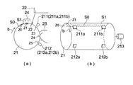
図4は、感光体上に形成されるパッチとパッチを検出するセンサとの説明図である。 FIG. 4 is an explanatory diagram of a patch formed on the photoconductor and a sensor for detecting the patch.
図4(a)は感光体21を側面から見た図で、図4(b)は、感光体21を斜め横から見た図(斜視図)である。なお、図4(b)では図を見易くするため露光部22と現像部23と帯電部24とを省略してある。
4A is a view of the
図4(a)と図4(b)において、矢印b方向に回転する感光体21の周囲には、感光体21の回転方向において、感光体を一様に帯電する帯電部24と、感光体21に潜像を形成する露光部22と、露光部22により形成された潜像の電位を測定する電位測定部である電位センサ211と、潜像をトナーで顕像化する現像部23と、トナー画像の濃度を測定する濃度測定部である濃度センサ212と、が配設されている。
4A and 4B, a charging
そして、感光体21が停止した時間を計測する計時部(以下計時部を画像形成停止タイマTMと称する。)が、感光体21が所定時間停止していたことを検出した時に、帯電部24に対向する感光体21の位置である帯電対向位置Z1を検出する検出部である感光体位相センサ213が感光体21に接続されている。
When the time measuring unit for measuring the time when the
ここで、電位センサ211は露光部22の下流側且つ現像部23の上流側に配設されており、濃度センサ212は現像部23の下流側且つ転写領域35(不図示)の上流側に配設されている。
Here, the
電位センサ211は、感光体21の軸方向に離間して設けられた第1電位センサ211aと第2電位センサ211bとで構成されている。
The
そして、第1電位センサ211aが後述の第1の潜像S1(不図示)と第3の潜像S3(不図示)との電位を測定し、第2電位センサ211bが後述の第2の潜像S2(不図示)と第4の潜像S4(不図示)との電位を測定する。
Then, the first
濃度センサ212は、感光体21の軸方向に離間して設けられた第1濃度センサ212aと第2濃度センサ212bとで構成されている。
The
そして、第1濃度センサ212aが前記第1の潜像S1を現像した後述の第1のパッチP1(不図示)と、前記第3の潜像S3を現像した後述の第3のパッチP3(不図示)と、の濃度を測定する。また、第2濃度センサ212bが前記第2の潜像S2を現像した後述の第2のパッチP2(不図示)と、前記第4の潜像S4を現像した第4のパッチP4(不図示)と、の濃度を測定する。
Then, a first patch P 1 below the
電位センサ211と、濃度センサ212と、感光体位相センサ213と、の出力はそれぞれ制御部Cに入力される。
Outputs of the
前述した、感光体21が停止した時間を計測する画像形成停止タイマTMにより感光体21が所定時間停止したことを検出した時に、帯電部24と対向する感光体21上の位置を帯電対向位置Z1と称する。
When it is detected by the image formation stop timer TM that measures the time that the
帯電対向領域S1は、感光体21上で感光体21と帯電部24とが帯電対向位置Z1において対向している領域である〔図4(b)一点鎖線〕。従って帯電対向領域S1は感光体21の回転に伴って矢印b方向に移動する。
The charging opposing region S1 is a region on the
そして、帯電対向領域S1は前述したように、画像形成が長時間行われず(感光体が回転せず)、帯電部24に対して感光体21の同一位置が長時間対向したような場合、感光体21と帯電部24とが対向した対向領域に残留するオゾンによってイオン生成物が生成され、該イオン生成物が感光体21に付着し、感光体表面の抵抗が低下する(像流れの発生)領域でもある。
As described above, when the image formation is not performed for a long time (the photoconductor does not rotate) and the same position of the
また、基準位置Z0は、感光体21の停止時間を計時する画像形成停止タイマTMが、感光体21が所定時間停止したことを検出した時に、感光体21と帯電部24との対向位置を外れた、像流れが発生しない、感光体の円周方向位置である。
Further, the reference position Z0 deviates from the position where the
そして、基準領域S0は、感光体21と帯電部24とが基準位置Z0において帯電部24と対向していない部分の感光体21の領域〔図4(b)破線〕である。従って基準位置Z0は感光体21の回転に伴って矢印b方向に移動する。
The reference region S0 is a region of the photosensitive member 21 (a broken line in FIG. 4B) where the
また、基準領域S0は感光体21が長時間停止してもイオン生成物が感光体21に付着しない領域でもある。
Further, the reference region S0 is a region where the ion product does not adhere to the
露光対向位置Z2は、露光部22の露光位置と対向する感光体21の円周方向位置である。従って基準位置Z2は感光体21が回転しても移動しない。
The exposure facing position Z <b> 2 is a circumferential position of the
感光体21の回転により帯電領域S1と基準領域S0とがそれぞれ露光対向位置Z2に到達すると、露光部22により前述の第1の潜像S1と第2の潜像S2と第3の潜像S3と第4の潜像S4とが感光体21上に形成される。
When the charged area S1 and the reference area S0 by the rotation of the
電位測定位置Z3は、電位センサ211と対向する感光体の円周方向位置である。従って基準位置Z3は感光体21が回転しても移動しない。
The potential measurement position Z3 is a circumferential position of the photoreceptor facing the
感光体21の回転により帯電領域S1と基準領域S0とがそれぞれ電位測定位置Z3に到達すると、露光対向位置Z2で形成された前述の第1の潜像S1〜第4の潜像S4の電位を電位センサ211が測定する。
When the rotation of the
現像対向位置Z4は、現像部23の現像位置と対向する感光体の円周方向位置である。従って基準位置Z4は感光体21が回転しても移動しない。
The development facing position Z4 is a circumferential position of the photoconductor facing the development position of the developing
感光体21の回転により帯電領域S1と基準領域S0とがそれぞれ現像対向位置Z4に到達すると、現像部23が露光対向位置Z2で形成された前述の第1の潜像S1〜第4の潜像S4を現像する。
When the rotation of the
濃度測定位置Z5は、濃度センサ212と対向する感光体21の円周方向位置である。従って基準位置Z5は感光体21が回転しても移動しない。
The density measurement position Z5 is a circumferential position of the
感光体21の回転により帯電領域S1と基準領域S0とがそれぞれ濃度測定位置Z5に到達すると、濃度センサ212が現像対向位置Z4に形成された前述の第1のパッチP1と第2のパッチP2と第3のパッチP3と第4のパッチP4との濃度を測定する。
When the charged area S1 and the reference area S0 by the rotation of the
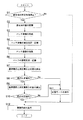
図5は、像流れ発生検知モードに係るフロー図である。 FIG. 5 is a flowchart according to the image flow occurrence detection mode.
以下図4と5を参照して、像流れの発生を検出する方法について説明する。図5に記したフローに係るプログラムは制御部Cの記憶部に格納されており、制御部CのCPUにより読み出されて実行される。 Hereinafter, a method for detecting the occurrence of image flow will be described with reference to FIGS. The program relating to the flow shown in FIG. 5 is stored in the storage unit of the control unit C, and is read and executed by the CPU of the control unit C.
図5に示す像流れ発生検知モードは像流れの発生を検出するモードで、機械の電源をオンした時、スリーピングモードから復帰した時など、機械が長時間放置された状態から復帰した時に画像形成停止タイマTMにより感光体21が所定時間停止したことを検出された場合に実行される。
The image flow occurrence detection mode shown in FIG. 5 is a mode for detecting the occurrence of image flow. When the machine is turned on or returned from the sleeping mode, an image is formed when the machine is returned from a state where it is left for a long time. This is executed when it is detected by the stop timer TM that the
1.感光体が所定時間停止したか否かの検知(ステップS1)
感光体21の停止時間を計時する前述の画像形成停止タイマTMが、感光体21の所定時間以上に亘る停止を検出した時(Yes)、制御部Cは像流れの可能性ありと判断して次ステップに進む。
1. Detection of whether or not the photoreceptor has stopped for a predetermined time (step S1)
When the above-described image formation stop timer TM that measures the stop time of the
画像形成停止タイマTMの計時が所定時間未満の時(No)は、感光体21が所定時間以上停止しておらず像流れの可能性なしと判断して画像形成を可能とするためステップS12に進む。
When the time of the image formation stop timer TM is less than the predetermined time (No), the
ここで、画像形成停止タイマTMの前記所定時間とは、像流れが発生しないと想定される最も長い感光体21の停止時間で、予め実験等により決定された値である。
Here, the predetermined time of the image formation stop timer TM is the longest stop time of the
2.感光体位置の記憶(ステップS2)
画像形成停止タイマTMが感光体21の所定時間以上に亘る停止を検出した時、感光体位相センサ213の出力を読み込んで帯電部24と対向している部分の感光体位置(図4の帯電対向位置Z1)を記憶する。即ち像流れの可能性がある部分を記憶する。
2. Storage of photoconductor position (step S2)
When the image formation stop timer TM detects the stop of the
同時に、帯電部24と対向していない感光体位置(図4の基準位置Z0)を記憶する。即ち像流れの可能性がない部分を記憶して、次ステップに進む。
At the same time, the photosensitive member position (reference position Z0 in FIG. 4) not facing the charging
3.パッチ潜像の形成(ステップS3)
感光体21の回転によって帯電対向位置Z1及び基準位置Z0が移動した現在位置を取得する。
3. Formation of patch latent image (step S3)
The current position where the charging facing position Z1 and the reference position Z0 are moved by the rotation of the
そして、帯電対向位置Z1及び基準位置Z0がそれぞれ露光部22の露光対向位置Z2に到達した時、露光部22は帯電対向位置Z1及び基準位置Z0に、それぞれ下記パッチに対応する潜像を形成する。
When the charging counter position Z1 and the reference position Z0 reach the exposure counter position Z2 of the
具体的には、感光体の帯電対向位置Z1が露光部22の露光対向位置Z2に到達した時、露光部22により、第1のパッチP1を形成する第1の潜像S1を第1の露光量L1で形成し、第2のパッチP2を形成する第2の潜像S2を第1の露光量L1より大きな第2の露光量L2で形成する。
Specifically, when the charge opposite position Z1 of the photosensitive member reaches the exposure position facing Z2 of the
また、感光体の基準位置Z0が露光部22の露光対向位置Z2に到達した時、露光部22により、第3のパッチP3を形成する第3の潜像S3を第1の露光量L1で形成し、第4のパッチP4を形成する第4の潜像S4を第2の露光量L2で形成し、次ステップに進む。
Further, when the reference position Z0 of the photosensitive member reaches the exposure position facing Z2 of the
なお、第1の露光量L1は、第1のパッチP1と第3のパッチP3とが像流れを起こさずに形成された時、その濃度が略20%となる露光量で、第2の露光量L2は、第2のパッチP2と第4のパッチP4とが像流れを起こさずに形成された時、その濃度が略70%となる露光量である。 The first exposure amount L 1 is an exposure amount at which the density becomes approximately 20% when the first patch P 1 and the third patch P 3 are formed without causing image flow. The exposure amount L 2 of 2 is an exposure amount at which the density becomes approximately 70% when the second patch P 2 and the fourth patch P 4 are formed without causing image flow.
濃度が略20%と略70%とする根拠は図2と図3とを参照して説明したように、像流れを起こす場合における電位と濃度に対して、流れを起こさない場合における電位と濃度が、大幅に異なり、検出し易いことによる。 The reason why the density is about 20% and about 70% is as described with reference to FIG. 2 and FIG. 3, as compared with the potential and density when the image flow is caused, and the potential and density when the flow is not caused. However, it is significantly different and easy to detect.
4.パッチ潜像の電位の測定(ステップS4)
感光体21の回転によって帯電対向位置Z1及び基準位置Z0が移動した現在位置を取得する。
4). Measurement of the potential of the patch latent image (step S4)
The current position where the charging facing position Z1 and the reference position Z0 are moved by the rotation of the
そして、帯電対向位置Z1及び基準位置Z0がそれぞれ電位測定位置Z3に到達した時、非接触式の電位センサ211は潜像の電位を測定する。
When the charging facing position Z1 and the reference position Z0 reach the potential measurement position Z3, the non-contact
このため、電位測定制御部(制御部C)は、電位測定部(電位センサ211)により感光体21上の帯電対向位置Z1を外れた基準位置Z0に露光部22により形成された潜像の電位を測定させ、電位測定部(電位センサ211)により帯電対向位置Z1に露光部22により形成された潜像の電位を測定させる。
For this reason, the potential measurement control unit (control unit C) detects the potential of the latent image formed by the
具体的には、感光体の帯電対向位置Z1が電位センサ211の電位測定位置Z3に到達した時、第1電位センサ211aで第1の潜像S1の電位(第1潜像電位E1)を測定し、第2電位センサ211bで第2の潜像S2の電位(第2潜像電位E2)を測定する。
Specifically, when the charge opposite position Z1 of the photosensitive member reaches the potential measurement position Z3 of the
また、感光体の基準位置Z0が電位センサ211の電位測定位置Z3に到達した時、第1電位センサ211aで第3の潜像S3の電位(第3潜像電位E3)を測定し、第2電位センサ211bで第4の潜像S4の電位(第4像電位E4)を測定する。
Further, when the reference position Z0 of the photosensitive member reaches the potential measurement position Z3 of the
そして、各測定値を記憶し次ステップに進む。 Then, each measured value is stored and the process proceeds to the next step.
5.パッチ潜像の現像(ステップS5)
感光体21の回転によって帯電対向位置Z1及び基準位置Z0が移動した現在位置を取得する。
5. Development of patch latent image (step S5)
The current position where the charging facing position Z1 and the reference position Z0 are moved by the rotation of the
そして、帯電対向位置Z1及び基準位置Z0がそれぞれ現像対向位置Z4に到達した時、現像部23はステップS3で形成した潜像を現像する。
When the charging facing position Z1 and the reference position Z0 reach the developing facing position Z4, the developing
具体的には、感光体の帯電対向位置Z1が現像対向位置Z4に到達した時、現像部23により、第1の潜像S1を現像して第1のパッチP1を形成し、第2の潜像S2を現像して第2のパッチP2を形成する。
Specifically, when the charge opposite position Z1 of the photoreceptor reaches the development position opposite Z4, the developing
また、感光体の基準位置Z0が現像対向位置Z4に到達した時、現像部23により、第3の潜像S3を現像して第3のパッチP3を形成し、第4の潜像S4を現像して第4のパッチP4を形成し、次ステップに進む。
Further, when the reference position Z0 of the photoreceptor reaches the development position opposite Z4, the developing
6.パッチの濃度測定(ステップS6)
感光体21の回転によって帯電対向位置Z1及び基準位置Z0が移動した現在位置を取得する。
6). Patch density measurement (step S6)
The current position where the charging facing position Z1 and the reference position Z0 are moved by the rotation of the
そして、帯電対向位置Z1及び基準位置Z0がそれぞれ濃度測定位置Z5に到達した時、濃度センサ212によりパッチの濃度測定を行う。
When the charging facing position Z1 and the reference position Z0 reach the density measurement position Z5, the
具体的には、感光体の帯電対向位置Z1が濃度センサ212の濃度測定位置Z5に到達した時、第1濃度センサ212aで第1のパッチP1の濃度を測定し(第1パッチ濃度D1)、第2濃度センサ212bで第2のパッチP2の濃度を測定する(第2パッチ濃度D2)。
Specifically, when the charge opposite position Z1 of the photosensitive member reaches the density measurement position Z5 of the
また、感光体の基準位置Z0が濃度センサ212の濃度測定位置Z5に到達した時、第1濃度センサ212aで第3のパッチP3の濃度を測定し(第3パッチ濃度D3)、第2濃度センサ212bで第4のパッチP4の濃度を測定する(第4パッチ濃度D4)。
Further, when the reference position Z0 of the photosensitive member reaches the density measurement position Z5 of the
そして、各測定値を記憶し次ステップに進む。 Then, each measured value is stored and the process proceeds to the next step.
7.基準電位と測定電位との差の算出(ステップS7)
像流れの発生のない基準位置Z0における潜像の電位に対するγカーブに相当する電位傾向と、像流れの発生の可能性がある帯電対向位置Z1における潜像の電位に対するγカーブに相当する電位傾向と、の差を類推する。
7). Calculation of difference between reference potential and measurement potential (step S7)
A potential tendency corresponding to the γ curve with respect to the potential of the latent image at the reference position Z0 where no image flow occurs, and a potential tendency corresponding to the γ curve with respect to the potential of the latent image at the charging facing position Z1 where image flow may occur. And analogy with the difference.
このため、基準位置Z0に形成された潜像の測定電位、即ち、基準位置Z0が感光体21の回転により電位測定部(電位センサ211)に対向する位置に到達した時に、電位センサ211が測定した基準位置Z0に形成された潜像の電位である基準電位と、帯電対向位置Z1に形成された潜像の測定電位、即ち、帯電対向位置Z1が、感光体21の回転により電位測定部(電位センサ211)に対向する位置に到達した時に、電位センサ211が測定した帯電対向位置Z1に形成された潜像の電位である帯電対向位置電位と、の差を算出する。
For this reason, the
具体的には、ステップS4で測定した、帯電対向位置電位の1つである第1の潜像S1の電位(第1潜像電位E1)と、基準電位の1つである第3の潜像S3の電位(第3潜像電位E3)と、の差である第1の電位差DfE1を算出する。 Specifically, measured in the step S4, the first latent image S 1 potential is one of the charging position opposed potential (a first latent image potential E 1), the third is one of the reference potential A first potential difference Df E1 , which is the difference between the potential of the latent image S 3 (third latent image potential E 3 ), is calculated.
また帯電対向位置電位の1つである第2の潜像S2の電位(第2潜像電位E2)と、基準電位の1つである第4の潜像S4の電位(第4潜像電位E4)と、の差である第2の電位差DfE2を算出し、次ステップに進む。 Further, the potential of the second latent image S 2 (second latent image potential E 2 ), which is one of the charging opposing position potentials, and the potential of the fourth latent image S 4 (fourth latent potential), which is one of the reference potentials. A second potential difference Df E2 which is the difference between the image potential E 4 ) and the image potential E 4 ) is calculated, and the process proceeds to the next step.
なお、第1の電位差DfE1を算出する場合には、像流れを起こさない第3潜像電位E3に相当する電位を予め実験等により求めておいて、第3潜像電位E3の替わりにこれを用いて算出しても良い。また、第2の電位差DfE2を算出する場合には、像流れを起こさない第4潜像電位E4に相当する電位を予め実験等により求めておいて、第4潜像電位E4の替わりにこれを用いて算出しても良い。 Incidentally, when calculating the first potential difference Df E1 is previously found through experiment or the like in advance a potential corresponding to the third latent image potential E 3 that does not cause image flow, instead of the third latent image potential E 3 It may be calculated using this. Also, when calculating the second potential difference Df E2 is previously found through experiment or the like in advance a potential corresponding to the fourth latent image potential E 4 which does not cause image flow, instead of the fourth latent image potential E 4 It may be calculated using this.
8.像流れ発生の判定(ステップS8)
ステップS7で算出した差が第1の所定値以上になった時に像流れが発生したと判断する。
8). Determination of occurrence of image flow (step S8)
When the difference calculated in step S7 exceeds the first predetermined value, it is determined that image flow has occurred.
具体的には、ステップS7で算出した第1の電位差DfE1及び第2の電位差DfE2のうち一方でも第1の所定値以上であれば(No)像流れが発生したと判断してステップS11に進み、第1の電位差DfE1及び第2の電位差DfE2の両者が第1の所定値未満であれば(Yes)電位は正常(像流れ発生可能性なし)と判断し次ステップに進む。 Specifically, if one of the first potential difference Df E1 and the second potential difference Df E2 calculated in step S7 is greater than or equal to the first predetermined value (No), it is determined that image flow has occurred and step S11 is performed. If both the first potential difference Df E1 and the second potential difference Df E2 are less than the first predetermined value (Yes), it is determined that the potential is normal (no image flow is likely to occur) and the process proceeds to the next step.
なお、像流れが発生したことの判断の確実性を期すために、第1の電位差DfE1及び第2の電位差DfE2の両者が第1の所定値以上であれば(No)像流れが発生したと判断してステップS11に進むようにしても良い。 In order to ensure the determination of the occurrence of image flow, if both the first potential difference Df E1 and the second potential difference Df E2 are equal to or greater than the first predetermined value (No), image flow occurs. You may make it determine that it carried out and to make it progress to step S11.
9.基準濃度と測定濃度との差の算出(ステップS9)
出力画像に像流れを発生しない基準位置Z0におけるトナー画像の濃度のγカーブと、出力画像に像流れの発生の可能性がある帯電対向位置Z1におけるトナー画像の濃度のγカーブと、の差を類推する。
9. Calculation of difference between reference concentration and measured concentration (step S9)
The difference between the γ curve of the density of the toner image at the reference position Z0 where no image flow occurs in the output image and the γ curve of the density of the toner image at the charging facing position Z1 where image flow may occur in the output image is calculated. Analogy.
このため、出力画像に像流れを発生しないパッチの濃度を前記濃度測定部(濃度センサ212)で測定した正常部分の濃度である基準濃度と、出力画像に像流れを発生するパッチの濃度を濃度センサ212で測定した異常部分の濃度である異常部測定濃度と、の差を算出する。
For this reason, the density of the patch that does not cause image flow in the output image is measured by the density measurement unit (density sensor 212), and the density of the patch that generates image flow in the output image is determined. The difference between the abnormal part measurement density which is the density of the abnormal part measured by the
具体的には、ステップS6で測定した、異常部測定濃度の1つである第1のパッチP1の濃度(第1パッチ濃度D1)と、基準濃度の1つである第3のパッチP3の濃度(第3パッチ濃度D3)との差である第1の濃度差DfD1を算出する。 Specifically, the density of the first patch P 1 (first patch density D 1 ), which is one of the abnormal part measured densities, and the third patch P, which is one of the reference densities, measured in step S6. A first density difference Df D1 that is a difference from the density of 3 (third patch density D 3 ) is calculated.
また、帯電対向位置電位の1つである第2のパッチP2の濃度(第2パッチ濃度D2)と、基準電位の1つである第4のパッチP4の濃度(第4パッチ濃度D4)との差である第2の濃度差DfD2を算出し、次ステップに進む。 Also, the density of the second patch P 2 (second patch density D 2 ), which is one of the charging opposing position potentials, and the density (fourth patch density D) of the fourth patch P 4 , which is one of the reference potentials. 4 ) A second density difference Df D2 that is a difference from the above is calculated, and the process proceeds to the next step.
なお、第1の濃度差DfD1を算出する場合には、像流れを起こさない第3パッチ濃度D3に相当する濃度を予め実験等により求めておいて、第3パッチ濃度D3の替わりにこれを用いて算出しても良い。また、第2の濃度差DfD2を算出する場合には、像流れを起こさない第4パッチ濃度D4に相当する濃度を予め実験等により求めておいて、第4パッチ濃度D4の替わりにこれを用いて算出しても良い。 Incidentally, when calculating the first concentration difference Df D1 is previously found through experiment or the like in advance the concentration corresponding to the third patch density D 3 which does not cause image blurring, instead of the third patch density D 3 You may calculate using this. Also, when calculating the second concentration difference Df D2 is previously found through experiment or the like in advance the concentration corresponding to the fourth patch density D 4 which does not cause image blurring, instead of the fourth patch density D 4 You may calculate using this.
10.像流れ発生の判定(ステップS10)
ステップS9で算出した差が第2の所定値以上になった時に像流れが発生したと判断する。
10. Determination of occurrence of image flow (step S10)
When the difference calculated in step S9 is greater than or equal to the second predetermined value, it is determined that image flow has occurred.
具体的には、ステップS9で算出した第1の濃度差DfD1及び第2の濃度差DfD2のうち一方でも所定値以上であれば(No)像流れが発生したと判断してステップS11に進み、第1の濃度差DfD1及び第2の濃度差DfD2の両者が所定値未満であれば(Yes)γ特性カーブは正常、即ち像流れ発生可能性なしと判断してステップS12に進む。 Specifically, if one of the first density difference Df D1 and the second density difference Df D2 calculated in step S9 is equal to or greater than a predetermined value (No), it is determined that image flow has occurred, and the process proceeds to step S11. If both the first density difference Df D1 and the second density difference Df D2 are less than a predetermined value (Yes), it is determined that the γ characteristic curve is normal, that is, there is no possibility of image flow, and the process proceeds to step S12. .
なお、像流れが発生したことの判断の確実性を期すために、第1の濃度差DfD1及び第2の濃度差DfD2の両者が第2の所定値以上であれば(No)像流れが発生したと判断してステップS11に進むようにしても良い。 In order to ensure the determination of the occurrence of the image flow, if both the first density difference Df D1 and the second density difference Df D2 are equal to or greater than the second predetermined value (No), the image flow is determined. It may be determined that the error has occurred and the process may proceed to step S11.
11.回復モードの実行(ステップS11)
感光体21の表面を研磨する後述の回復モードを実行し、回復モードが終了したら次ステップに進む。
11. Execution of recovery mode (step S11)
A recovery mode, which will be described later, for polishing the surface of the
12.画像形成の実行(ステップS12)
ジョブに応じた画像形成を開始、もしくは再開し、エンドに進む。
12 Execution of image formation (step S12)
Start or restart image formation according to the job, and proceed to the end.
なお、ステップS11による回復モードを実行後の、ステップS12における画像形成の場合は、ステップS2〜ステップS11を実行して像流れの発生の可能性がないことを確認後、ジョブに応じた画像形成を開始、もしくは再開しても良い。 In the case of image formation in step S12 after executing the recovery mode in step S11, it is confirmed that there is no possibility of image flow by executing steps S2 to S11, and then image formation corresponding to the job is performed. May be started or resumed.
また、ステップS8の像流れ発生の判定において、ステップS7で算出した第1の電位差DfE1及び第2の電位差DfE2がそれぞれ所定値未満であれば(Yes)、濃度異常の要因である電位異常がないため、像流れの発生可能性なしと判断してステップS9とステップS10とを実行せずに(濃度による判定は行わずに)ステップS12に進むようにしても良い。 Further, in the determination of the occurrence of image flow in step S8, if the first potential difference Df E1 and the second potential difference Df E2 calculated in step S7 are each less than a predetermined value (Yes), the potential abnormality that is a cause of density abnormality Therefore, it may be determined that there is no possibility of image flow and step S9 and step S10 are not executed (the determination based on the density is not performed), and the process may proceed to step S12.
そして、この場合は濃度測定に関するステップS5とステップS6とを実行せずステップS4からステップS7へ進めても良い。 In this case, step S5 and step S6 relating to density measurement may not be executed, and the process may proceed from step S4 to step S7.
また、ステップS8とステップS9とを行わず、ステップS10の像流れ発生の判定において、ステップS9で算出した第1の濃度差DfD1及び第2の濃度差DfD2の少なくとも一方が第2の所定値以上であれば(No)、像流れが発生した判断してステップS11に進め、第1の濃度差DfD1及び第2の濃度差DfD2がそれぞれ所定値未満であれば(Yes)、像流れの発生なしと判断してステップS12に進むようにしても良い。 Further, step S8 and step S9 are not performed, and in the determination of image flow occurrence in step S10, at least one of the first density difference Df D1 and the second density difference Df D2 calculated in step S9 is a second predetermined value. If it is equal to or greater than the value (No), it is determined that image flow has occurred, and the process proceeds to step S11. If the first density difference Df D1 and the second density difference Df D2 are each less than a predetermined value (Yes), the image is displayed. It may be determined that no flow has occurred and the process may proceed to step S12.
そして、この場合は電位測定に関するステップS4を実行せずステップS3からステップS5へ進めても良い。 In this case, step S4 relating to the potential measurement may not be performed and the process may proceed from step S3 to step S5.
以上説明したように、感光体に形成された潜像の電位、そして/又は感光体に担持されたトナー画像の濃度、を測定することで、確実に像流れの発生を検出し、像流れの発生がないにもかかわらず像流れと誤検出することを防止可能となる。 As described above, by measuring the potential of the latent image formed on the photoconductor and / or the density of the toner image carried on the photoconductor, it is possible to reliably detect the occurrence of image flow and It is possible to prevent erroneous detection of image flow despite no occurrence.
なお前述の、帯電部24と、露光部22と、電位測定部211と、計時部(画像形成停止タイマTM)と、検出部(感光体位相センサ213)と、電位測定制御部と判断部(制御部の一機能)とは、像流れを検知する像流れ検知装置としても機能している。
Note that the charging
図6は、感光体表面修復部の説明図(側面図)である。 FIG. 6 is an explanatory diagram (side view) of the photosensitive member surface repair portion.
感光体21の表面を研磨する感光体表面修復部5は少なくともクリーニング部52を有しており、前記基準電位と前記帯電対向位置電位との差が第1の所定値以上になった時に像流れが発生したと判断する判断部(制御部C)が、像流れが発生したと判断した場合、感光体表面修復部5は感光体21の表面を研磨する。
The photoconductor
以下、感光体表面修復部5がクリーニング部52とクリーニングブレード51とを有している場合について説明する。
Hereinafter, the case where the photoconductor
クリーニングブレード51は、その先端部511が感光体21に当接しており、先端部511が回転する感光体21を摺擦することにより先端部511に付着したトナーが感光体21の表面を研磨すると同時に、感光体21に残留したトナーを除去する。
The
クリーニング部52は、クリーニングブラシ部53と、フリッカローラ部54と、を有している。
The
そして、クリーニングブラシ部53は、回転軸531と、回転軸531の表面に放射状に植毛されたブラシ532と、ブラシ532を矢印c方向に回転させる回転駆動部533と、を有している。
The cleaning
そして、ポリエステル系材料より成るループ状をしたブラシ532の先端部534は感光体21に当接しており、ブラシ532の回転により先端部534が感光体21を摺擦することにより、ブラシ532に付着したトナーが感光体21の表面を研磨する。
The
なお、ブラシ532の形状をループ状としたことで、ブラシ532にトナーを保持し易くし、感光体21の研磨性を向上させている。
In addition, by making the shape of the
フリッカローラ部54は、クリーニングブラシ部53のブラシ532に摺接し、接地しているフリッカローラ541と、フリッカローラ541を感光体21に向けて移動可能なローラ移動部543と、を有している。
The
そして、ローラ移動部543は、ブラシ532に対するフリッカローラ541の位置を調整可能としている。
The
ここで、フリッカローラ541とブラシ532との重なりが大きくなるとフリッカローラ541がブラシ532を摺擦する力が大きくなり(ブラシ532に付着するトナーを弾き出す力が増加し)、ブラシ532に付着するトナーの量が少なくなってブラシ532による感光体21表面の研磨が少なくなる。
Here, when the overlap between the
また、フリッカローラ541とブラシ532との重なりが小さくなるとフリッカローラ541がブラシ532を摺擦する力が小さくなり(ブラシ532に付着するトナーを弾き出す力が減少し)、ブラシ532に付着するトナーの量が多くなってブラシ532による感光体21表面の研磨が多くなる。
Further, when the overlap between the
以上の説明において、感光体表面修復部5にクリーニングブレード51を設けない場合は、感光体表面修復部5の下流側に感光体21に残留したトナーを除去するクリーニングブレード51を設ける。
In the above description, when the
以下、図6を参照して感光体表面の修復に係る方法の説明を行う。 Hereinafter, a method for repairing the surface of the photoreceptor will be described with reference to FIG.
なお、以下に説明する感光体表面の修復は前述の像流れ発生検知モードに係るフロー図において、ステップS11の回復モードの実行に対応する。 Note that the photoconductor surface repair described below corresponds to the execution of the recovery mode in step S11 in the flowchart relating to the above-described image flow occurrence detection mode.
また、以下に説明する複数の形態の回復モードのうち、いずれか1つを実行しても良いが、複数の形態の回復モードを同時に実行しても良い。 In addition, any one of a plurality of recovery modes described below may be executed, but a plurality of recovery modes may be executed simultaneously.
第1の形態の回復モードについて説明する。 The recovery mode of the first form will be described.
前記判断部である制御部Cが像流れが発生したと判断した場合、現在のクリーニングブラシ部53のブラシ532の回転数に対して、回転駆動部533によりブラシ532の回転数を変化することにより、ブラシ532と感光体21の表面との相対速度を上げ、ブラシ532に付着したトナーによる感光体21の表面の研磨能力を向上させる。
When the control unit C, which is the determination unit, determines that image flow has occurred, the rotation number of the
ブラシ532先端の回転速度は、例えば通常時570mm/Sに対し330mm/Sに下げることが好ましい。
For example, the rotational speed of the tip of the
そして研磨能力を向上させた状態で画像形成を所定時間行い、所定時間経過後にブラシ532の回転数を元に戻す。
Then, image formation is performed for a predetermined time in a state where the polishing ability is improved, and the rotational speed of the
なお、クリーニングブレード51は、先端部511が回転する感光体21を摺擦することにより先端部511に付着したトナーが感光体21の表面を研磨すると同時に、感光体21に残留したトナーを除去する。
The
以上説明したように、ブラシ532の回転数を変化することによりブラシ532と感光体21の表面との相対速度を上げてブラシ532に付着したトナーによる感光体21の表面の研磨能力を向上させることができる。
As described above, by changing the number of rotations of the
第2の形態の回復モードについて説明する。 The recovery mode of the second form will be described.
判断部(制御部C)が、像流れが発生したと判断した場合、クリーニングブレード51及びブラシ532に付着するトナーの量を増加する。
When the determination unit (control unit C) determines that image flow has occurred, the amount of toner attached to the
具体的には、1ページ分のトナー画像の間に形成するトナー帯のトナー量を増加させ、トナー量を増加した前記トナー帯を用紙Pに転写させず、そのまま感光体表面修復部5まで搬送させる。
Specifically, the toner amount of the toner band formed between the toner images for one page is increased, and the toner band with the increased toner amount is not transferred to the paper P and is conveyed as it is to the photoreceptor
なお、トナー帯のトナー量の増加は実験等により予め求めた値で、副走査方向のトナー帯の幅を通常時の幅が例えば1mmに対して、付着トナー量を増加させる時には例えば5mmに上げることが好ましい。 The increase in the toner amount of the toner band is a value obtained in advance by experiments or the like, and the width of the toner band in the sub-scanning direction is increased to, for example, 5 mm when the amount of adhered toner is increased, while the normal width is, for example, 1 mm. It is preferable.
そして、幅が増加したトナー帯のトナーを感光体表面修復部5のブラシ532に付着させ、増加した付着トナーによって感光体21の表面の研磨能力を向上させる。
Then, the toner in the toner band having an increased width is attached to the
そして研磨能力を向上させた状態で画像形成を所定時間行い、所定時間経過後にトナー帯の単位面積当たりのトナー量を元に戻す。 Then, image formation is performed for a predetermined time with the polishing ability improved, and the toner amount per unit area of the toner band is restored after the predetermined time has elapsed.
なお、クリーニングブレード51は、先端部511が回転する感光体21を摺擦することにより、先端部511に付着したより多くのトナーが感光体21の表面を研磨すると同時に、感光体21に残留したトナーを除去する。
The
以上説明したように、トナー帯の幅を大きくすることによりブラシ532とクリーニングブレード51に付着するトナー量を増加させて、ブラシ532とクリーニングブレード51に付着したトナーによる感光体21の表面の研磨能力をより向上させることができる。
As described above, the toner amount attached to the
第3の形態の回復モードについて説明する。 A third mode of recovery mode will be described.
判断部(制御部C)が像流れが発生したと判断した場合、ブラシ532に対する現在のフリッカローラ541の位置に対して、フリッカローラ541のブラシ532に対する相対距離を大きくする。
When the determination unit (control unit C) determines that image flow has occurred, the relative distance of the
これにより、ブラシ532に対するフリッカローラ541の重なり量が少なくなり、ブラシ532に付着したトナーを弾き出す力が減少する。結果としてブラシ532に付着するトナーの量が多くなり、ブラシ532に付着したトナーによる感光体21の表面の研磨能力を向上させることができる。
Thereby, the amount of overlap of the
なお、ブラシ532に対するフリッカローラ541の重なり量は実験等により予め求めた値で、通常時は例えば0.6mmに対して、付着トナー量を増加させる時には例えば0mmにすることが好ましい。
Note that the overlap amount of the
そして研磨能力を向上させた状態で所定時間画像形成を行い、所定時間経過後にフリッカローラ541のブラシ532に対する距離を元に戻す。
Then, image formation is performed for a predetermined time with the polishing ability improved, and the distance of the
なお、クリーニングブレード51は、先端部511が回転する感光体21を摺擦することにより先端部511に付着したトナーが感光体21の表面を研磨すると同時に、感光体21に残留したトナーを除去する。
The
以上説明したように、ブラシ532に対するフリッカローラ541の相対距離を大きくすることによりブラシ532に付着するトナー量を増加させて、ブラシ532に付着したトナーによる感光体21の表面の研磨能力を向上させることができる。
As described above, the amount of toner adhering to the
第1の形態の回復モードと第2の形態の回復モードと第3の形態の回復モードについて、研磨能力を向上させた状態で所定時間画像形成を行うものとして説明したが、研磨能力を向上させた状態で所定枚数分の画像形成を行うようにしても良い。 The recovery mode of the first mode, the recovery mode of the second mode, and the recovery mode of the third mode have been described as performing image formation for a predetermined time in a state where the polishing capability is improved. In this state, a predetermined number of images may be formed.
以上、感光体表面修復部5にクリーニングブレード51とクリーニングブラシ部53とを設けた構成に係る回復モードについて説明したが、感光体表面修復部5にクリーニングブラシ部53のみを設けてクリーニングブラシ部53で感光体21の表面を研磨するようにしても良い。
The recovery mode according to the configuration in which the
この場合は、感光体表面修復部5において、以上説明したクリーニングブレード51に係る作用はなく、クリーニングブラシ部53に係る作用のみとなる。
In this case, the photosensitive member
そして、感光体表面修復部5の下流側に配設されたクリーニングブレード51は感光体21に残留したトナーを除去する作用が中心となり、特に第2の形態の回復モードにおいては感光体表面修復部5に搬送されるトナー量が増加するため従の作用として感光体21の表面を研磨する作用を有している。
The
以上説明したように、像流れの発生を検出可能とし、検出した場合は感光体表面を効率的に研磨することができ、像流れの発生を防止することが可能となる。 As described above, it is possible to detect the occurrence of image flow, and when it is detected, the surface of the photoconductor can be efficiently polished, and the occurrence of image flow can be prevented.
以上モノクロの画像形成装置を例に挙げて説明したがカラーの画像形成装置A’に、前述の像流れの検出と、感光体表面修復部5とを適用できることは言うまでもなく、図7にカラーの画像形成装置A’に感光体表面修復部5を適応した場合の構成を示す。
The monochrome image forming apparatus has been described above as an example. Needless to say, the color image forming apparatus A ′ can be applied to the above-described image flow detection and the photoreceptor
図7はカラーの画像形成装置の説明図である。 FIG. 7 is an explanatory diagram of a color image forming apparatus.
なお、前述のモノクロ画像形成装置と同様な機能を有する部材には同様な部番を付してある。このため同様な部材については説明を省略する。 Members having the same functions as those of the monochrome image forming apparatus described above are given the same part numbers. For this reason, description of similar members is omitted.
エンドレスベルト状の中間転写体28は、ローラ281、282、283、284により回転可能に張架されており、不図示の駆動装置によりローラ283を介して矢印a’方向に駆動されている。
The endless belt-shaped intermediate transfer member 28 is rotatably stretched by
中間転写体28には各色用の感光体21(21Y、21M、21C、21K)が対向して設けられ、各色の感光体21(21Y、21M、21C、21K)にはそれぞれ前述した、帯電部24と、露光部22と、電位センサ211と、現像部23と、濃度センサ212と、感光体表面修復部5と、がそれぞれ配置されている。そして感光体毎に、像流れの検出と、像流れの発生検出時に当該感光体表面の研磨と、を行っている。
The intermediate transfer member 28 is provided with the photosensitive members 21 (21Y, 21M, 21C, and 21K) for the respective colors facing each other. 24, the
そして、2次転写ローラ36の押圧により中間転写体28に担持されたカラーのトナー画像が用紙Pに一括転写される。また、用紙Pに転写されず中間転写体28に残留したトナーはクリーニング部29により除去する。
Then, the color toner images carried on the intermediate transfer body 28 are collectively transferred onto the paper P by the pressing of the
なお、クリーニング部29を設けず、感光体表面修復部5のクリーニングブレード51で残留したトナーを除去させても良いことは言うまでもない。
Needless to say, the
この場合は各感光体でそれぞれ像流れの検出と、像流れの検出時には当該感光体の研磨と、が可能となり、像流れによる出力画像の品質低下を防止できる。 In this case, it is possible to detect the image flow on each photoconductor and to polish the photoconductor when detecting the image flow, and to prevent the output image from being degraded due to the image flow.
他の形態として、電位センサ211と濃度センサ212とを各感光体に配置せず、感光体表面修復部5を各感光体21に対向して配置し、濃度センサ212(不図示)を中間転写体28に対向して配置しても良い。
As another form, the
この場合は、中間転写体28において、2次転写部37の下流側且つクリーニング部29の上流側に濃度センサ212を設け、感光体21において、転写部27の下流側且つ帯電部24の上流側に感光体表面修復部5を設け、中間転写体28に配置された濃度センサ212によりカラートナーパッチの濃度測定により像流れの検出を行い、像流れの発生検出時には感光体21に配置された感光体表面修復部5で感光体21の研磨を行う。
In this case, a
また、この場合は中間転写体28に対向して感光体表面修復部5を設けてもよく、感光体表面修復部5により汚れた中間転写体28の表面を研磨可能となる。
In this case, the photosensitive member
以上説明したように、カラーの画像形成装置においても、像流れの発生を検出可能とし、検出した場合は感光体表面を効率的に研磨することができ、像流れの発生を防止することが可能となる。 As described above, even in a color image forming apparatus, it is possible to detect the occurrence of image flow, and if detected, the surface of the photoconductor can be polished efficiently, and the occurrence of image flow can be prevented. It becomes.
5 感光体表面修復部
21 感光体
22 露光部
23 現像部
24 帯電部
28 クリーニング部
51 クリーニングブレード
52 クリーニング部
53 クリーニングブラシ部
54 フリッカローラ部
211 電位センサ
212 濃度センサ
213 感光体位相センサ
532 ブラシ
A 画像形成装置
C 制御部
DESCRIPTION OF
Claims (16)
前記感光体に潜像を形成する露光部と、
前記感光体に対向して設けられ前記露光部により形成された潜像の電位を測定する電位測定部と、
前記感光体が停止していた時間を計測する計時部と、
前記計時部が前記感光体が所定時間停止していたことを検出した時に、前記帯電部に対向する前記感光体の位置である帯電対向位置を検出する検出部と、
前記感光体上の前記帯電対向位置を外れた基準位置に前記露光部により形成された潜像の電位を測定した基準電位と、前記帯電対向位置に前記露光部により形成された潜像の電位を測定した帯電対向位置電位と、を前記電位測定部で測定する電位測定制御部と、
前記基準電位と前記帯電対向位置電位との差が第1の所定値以上になった時に像流れが発生したと判断する判断部と、
を有することを特徴とする像流れ検知装置。 A charging unit that uniformly charges the photoconductor;
An exposure unit for forming a latent image on the photoreceptor;
An electric potential measuring unit for measuring the electric potential of the latent image formed by the exposure unit provided facing the photoconductor;
A time measuring unit for measuring the time during which the photosensitive member is stopped;
A detection unit that detects a charging facing position that is a position of the photosensitive member facing the charging unit when the timing unit detects that the photosensitive member has been stopped for a predetermined time; and
A reference potential obtained by measuring the potential of the latent image formed by the exposure unit at a reference position off the charging counter position on the photoconductor, and a potential of the latent image formed by the exposure unit at the charging counter position. A potential measurement control unit that measures the measured charge-facing position potential and the potential measurement unit;
A determination unit that determines that an image flow has occurred when a difference between the reference potential and the charging counter position potential is equal to or greater than a first predetermined value;
An image flow detection device comprising:
前記帯電対向位置電位は、前記帯電対向位置が、前記感光体の回転により前記電位測定部に対向する位置に到達した時に、前記電位測定部が測定した前記帯電対向位置に形成された潜像の電位である、
ことを特徴とする請求項1に記載の像流れ検知装置。 The reference potential is a potential of a latent image formed at the reference position measured by the potential measurement unit when the reference position reaches a position facing the potential measurement unit by rotation of the photoconductor,
The charging counter position potential is determined based on the latent image formed at the charging counter position measured by the potential measuring unit when the charging counter position reaches a position facing the potential measuring unit by rotation of the photoconductor. Is a potential,
The image flow detection apparatus according to claim 1, wherein
前記判断部は、前記第3の潜像の電位である第3潜像電位と、前記第1の潜像の電位である第1潜像電位と、の差である第1の電位差が、前記第1の所定値以上になった時に像流れが発生したと判断する、
ことを特徴とする請求項2に記載の像流れ検知装置。 The exposure unit forms a first latent image forming a first patch with a first exposure amount at the charging facing position, and forms a second latent image forming a second patch on the first latent image. A third latent image is formed with a second exposure amount larger than the exposure amount, and a third latent image for forming a third patch is formed with the first exposure amount at the reference position, thereby forming a fourth patch. 4 latent images are formed with the second exposure amount,
The determination unit has a first potential difference that is a difference between a third latent image potential that is a potential of the third latent image and a first latent image potential that is a potential of the first latent image, It is determined that image flow has occurred when the first predetermined value is exceeded.
The image flow detection device according to claim 2, wherein
前記現像部により形成された、前記第1のパッチと前記第2のパッチと前記第3のパッチと前記第4のパッチとの濃度を測定する濃度測定部と、を有し、
前記判断部は、前記第1のパッチの濃度を前記濃度測定部で測定した濃度である基準濃度と、前記第3のパッチの濃度を前記濃度測定部で測定した濃度である帯電対向位置濃度と、の差が第2の所定値以上になった時に像流れが発生したと判断することを特徴とする請求項3又は4に記載の像流れ検知装置。 A developing unit for developing the latent image formed on the photoreceptor;
A density measuring unit that measures the density of the first patch, the second patch, the third patch, and the fourth patch formed by the developing unit;
The determination unit includes a reference density which is a density measured by the density measuring unit with respect to the density of the first patch, and a charged counter position density which is a density measured with the density measuring unit. 5. The image flow detection device according to claim 3, wherein an image flow is determined to occur when the difference between the first and second values exceeds a second predetermined value. 6.
前記帯電対向位置濃度は、前記帯電対向位置が前記感光体の回転により前記濃度測定部に対向する位置に到達した時に、前記濃度測定部が測定した前記帯電対向位置に形成されたパッチの濃度である、
ことを特徴とする請求項5に記載の像流れ検知装置。 The reference density is a density of a patch formed at the reference position measured by the density measurement unit when the reference position reaches a position facing the density measurement unit by rotation of the photoconductor,
The density of the charging counter position is a density of the patch formed at the charging counter position measured by the density measuring unit when the charging counter position reaches a position facing the density measuring unit by rotation of the photoconductor. is there,
The image flow detection device according to claim 5.
前記判断部は、前記第3のパッチの濃度である第3パッチ濃度と、前記第1のパッチの濃度である第1パッチ濃度と、の差である第1の濃度差が、前記第2の所定値以上になった時に像流れが発生したと判断する、
ことを特徴とする請求項5又は6に記載の像流れ検知装置。 The developing unit forms the first patch and the second patch at the charging facing position, and forms the third latent image and the fourth patch at the reference position,
The determination unit determines that a first density difference, which is a difference between a third patch density that is the density of the third patch and a first patch density that is the density of the first patch, is the second density. It is determined that image drift has occurred when the value exceeds a predetermined value.
The image flow detection device according to claim 5 or 6, wherein
前記判断部が、像流れが発生したと判断した場合前記感光体の表面を研磨する感光体表面修復部を有し、
前記感光体表面修復部は、回転可能なクリーニングブラシと、前記クリーニングブラシでかきとったトナーを回収するフリッカローラと、前記クリーニングブラシを前記感光体に向けて移動可能なブラシ移動部と、を有し、
前記クリーニングブラシのブラシ先端部は前記感光体に当接しており、前記クリーニングブラシの回転により前記ブラシ先端部が前記感光体を摺擦することにより、前記クリーニングブラシに付着したトナーで前記感光体の表面を研磨する、
ことを特徴とする画像形成装置。 An image forming apparatus comprising the image flow detection device according to claim 1,
The determination unit has a photoconductor surface repair unit that polishes the surface of the photoconductor when it is determined that image flow has occurred,
The photoconductor surface repair unit includes a rotatable cleaning brush, a flicker roller that collects toner scraped by the cleaning brush, and a brush moving unit that can move the cleaning brush toward the photoconductor. And
The brush tip of the cleaning brush is in contact with the photoconductor, and the brush tip is rubbed against the photoconductor by the rotation of the cleaning brush. Polishing the surface,
An image forming apparatus.
トナー量を増加した前記トナー帯を前記感光体表面修復部まで搬送させることにより、前記クリーニングブラシに付着するトナー量を増加することを特徴とする請求項11に記載の画像形成装置。 Increasing the amount of toner per unit area of the toner band formed between toner images for one page,
The image forming apparatus according to claim 11, wherein the toner amount attached to the cleaning brush is increased by transporting the toner band having an increased toner amount to the photoconductor surface repair unit.
前記クリーニングブレードはその先端部が前記感光体に当接しており、前記先端部が回転する前記感光体を摺擦することにより前記先端部に付着したトナーで前記感光体の表面を研磨することを特徴とする請求項9〜13のいずれか1項に記載の画像形成装置。 The photoconductor surface repair portion has a cleaning blade for removing toner remaining on the photoconductor,
The cleaning blade has a front end in contact with the photoconductor, and the surface of the photoconductor is polished with toner adhering to the front end by rubbing the photoconductor rotating the front end. The image forming apparatus according to claim 9, wherein the image forming apparatus is an image forming apparatus.
トナー量を増加した前記トナー帯を前記感光体表面修復部まで搬送させることにより、前記クリーニングブレードに付着するトナー量を増加することを特徴とする請求項15に記載の画像形成装置。 Increase the amount of toner in the toner band formed between the toner images for one page,
The image forming apparatus according to claim 15, wherein the toner amount attached to the cleaning blade is increased by transporting the toner band having an increased toner amount to the photoconductor surface repair unit.
Priority Applications (1)
| Application Number | Priority Date | Filing Date | Title |
|---|---|---|---|
| JP2011047295A JP2012185257A (en) | 2011-03-04 | 2011-03-04 | Image deletion detection device and image forming apparatus |
Applications Claiming Priority (1)
| Application Number | Priority Date | Filing Date | Title |
|---|---|---|---|
| JP2011047295A JP2012185257A (en) | 2011-03-04 | 2011-03-04 | Image deletion detection device and image forming apparatus |
Publications (1)
| Publication Number | Publication Date |
|---|---|
| JP2012185257A true JP2012185257A (en) | 2012-09-27 |
Family
ID=47015417
Family Applications (1)
| Application Number | Title | Priority Date | Filing Date |
|---|---|---|---|
| JP2011047295A Withdrawn JP2012185257A (en) | 2011-03-04 | 2011-03-04 | Image deletion detection device and image forming apparatus |
Country Status (1)
| Country | Link |
|---|---|
| JP (1) | JP2012185257A (en) |
Cited By (5)
| Publication number | Priority date | Publication date | Assignee | Title |
|---|---|---|---|---|
| CN103941560A (en) * | 2013-01-18 | 2014-07-23 | 佳能精技股份有限公司 | Image forming apparatus |
| JP2014137551A (en) * | 2013-01-18 | 2014-07-28 | Canon Finetech Inc | Image forming apparatus |
| JP2014137552A (en) * | 2013-01-18 | 2014-07-28 | Canon Finetech Inc | Image forming apparatus |
| JP2015155962A (en) * | 2014-02-20 | 2015-08-27 | 京セラドキュメントソリューションズ株式会社 | Photoreceptor refresh device and image forming apparatus |
| JP2020140127A (en) * | 2019-02-28 | 2020-09-03 | キヤノン株式会社 | Method of controlling electrophotographic device |
-
2011
- 2011-03-04 JP JP2011047295A patent/JP2012185257A/en not_active Withdrawn
Cited By (5)
| Publication number | Priority date | Publication date | Assignee | Title |
|---|---|---|---|---|
| CN103941560A (en) * | 2013-01-18 | 2014-07-23 | 佳能精技股份有限公司 | Image forming apparatus |
| JP2014137551A (en) * | 2013-01-18 | 2014-07-28 | Canon Finetech Inc | Image forming apparatus |
| JP2014137552A (en) * | 2013-01-18 | 2014-07-28 | Canon Finetech Inc | Image forming apparatus |
| JP2015155962A (en) * | 2014-02-20 | 2015-08-27 | 京セラドキュメントソリューションズ株式会社 | Photoreceptor refresh device and image forming apparatus |
| JP2020140127A (en) * | 2019-02-28 | 2020-09-03 | キヤノン株式会社 | Method of controlling electrophotographic device |
Similar Documents
| Publication | Publication Date | Title |
|---|---|---|
| US9031430B2 (en) | Image forming apparatus | |
| JP2012185257A (en) | Image deletion detection device and image forming apparatus | |
| JP4946081B2 (en) | Image forming apparatus | |
| JP4901294B2 (en) | Image forming apparatus and image forming method | |
| JP6548398B2 (en) | Image forming device | |
| JP5452509B2 (en) | Image forming apparatus | |
| JP2012155116A (en) | Image forming apparatus | |
| JP4780201B2 (en) | Image forming apparatus | |
| JP2010079066A (en) | Image forming apparatus | |
| JP2009086234A (en) | Image forming apparatus | |
| JP6053390B2 (en) | Image forming apparatus | |
| JP2010128400A (en) | Image forming apparatus | |
| JP6314025B2 (en) | Image forming apparatus, transfer current control method, and transfer current control program | |
| JP2016075768A (en) | Image forming apparatus | |
| US11169469B2 (en) | Image forming apparatus | |
| JP2010002528A (en) | Image forming apparatus | |
| JP2009122343A (en) | Image forming apparatus | |
| JP6129109B2 (en) | Image forming apparatus | |
| JP7071232B2 (en) | Image forming device | |
| JP2016130830A (en) | Image forming apparatus | |
| JP2010276854A (en) | Image forming apparatus | |
| JP2009192568A (en) | Image forming apparatus, and control program for image forming processing | |
| JP3542148B2 (en) | Image forming device | |
| JP5146069B2 (en) | Contact state control device and image forming apparatus. | |
| JP6064334B2 (en) | Image forming apparatus and image forming program |
Legal Events
| Date | Code | Title | Description |
|---|---|---|---|
| A711 | Notification of change in applicant |
Free format text: JAPANESE INTERMEDIATE CODE: A712 Effective date: 20130415 |
|
| A300 | Withdrawal of application because of no request for examination |
Free format text: JAPANESE INTERMEDIATE CODE: A300 Effective date: 20140513 |