JP2012169625A - Led device - Google Patents
Led device Download PDFInfo
- Publication number
- JP2012169625A JP2012169625A JP2012027982A JP2012027982A JP2012169625A JP 2012169625 A JP2012169625 A JP 2012169625A JP 2012027982 A JP2012027982 A JP 2012027982A JP 2012027982 A JP2012027982 A JP 2012027982A JP 2012169625 A JP2012169625 A JP 2012169625A
- Authority
- JP
- Japan
- Prior art keywords
- light emitting
- led
- parallel
- series
- emitting element
- Prior art date
- Legal status (The legal status is an assumption and is not a legal conclusion. Google has not performed a legal analysis and makes no representation as to the accuracy of the status listed.)
- Pending
Links
- 230000000903 blocking effect Effects 0.000 claims description 16
- 230000007423 decrease Effects 0.000 claims description 16
- 239000004065 semiconductor Substances 0.000 claims description 16
- 238000010586 diagram Methods 0.000 description 20
- 230000002159 abnormal effect Effects 0.000 description 2
Images


Classifications
-
- H—ELECTRICITY
- H05—ELECTRIC TECHNIQUES NOT OTHERWISE PROVIDED FOR
- H05B—ELECTRIC HEATING; ELECTRIC LIGHT SOURCES NOT OTHERWISE PROVIDED FOR; CIRCUIT ARRANGEMENTS FOR ELECTRIC LIGHT SOURCES, IN GENERAL
- H05B45/00—Circuit arrangements for operating light-emitting diodes [LED]
- H05B45/30—Driver circuits
- H05B45/37—Converter circuits
-
- H—ELECTRICITY
- H05—ELECTRIC TECHNIQUES NOT OTHERWISE PROVIDED FOR
- H05B—ELECTRIC HEATING; ELECTRIC LIGHT SOURCES NOT OTHERWISE PROVIDED FOR; CIRCUIT ARRANGEMENTS FOR ELECTRIC LIGHT SOURCES, IN GENERAL
- H05B45/00—Circuit arrangements for operating light-emitting diodes [LED]
- H05B45/50—Circuit arrangements for operating light-emitting diodes [LED] responsive to malfunctions or undesirable behaviour of LEDs; responsive to LED life; Protective circuits
- H05B45/54—Circuit arrangements for operating light-emitting diodes [LED] responsive to malfunctions or undesirable behaviour of LEDs; responsive to LED life; Protective circuits in a series array of LEDs
-
- Y—GENERAL TAGGING OF NEW TECHNOLOGICAL DEVELOPMENTS; GENERAL TAGGING OF CROSS-SECTIONAL TECHNOLOGIES SPANNING OVER SEVERAL SECTIONS OF THE IPC; TECHNICAL SUBJECTS COVERED BY FORMER USPC CROSS-REFERENCE ART COLLECTIONS [XRACs] AND DIGESTS
- Y02—TECHNOLOGIES OR APPLICATIONS FOR MITIGATION OR ADAPTATION AGAINST CLIMATE CHANGE
- Y02B—CLIMATE CHANGE MITIGATION TECHNOLOGIES RELATED TO BUILDINGS, e.g. HOUSING, HOUSE APPLIANCES OR RELATED END-USER APPLICATIONS
- Y02B20/00—Energy efficient lighting technologies, e.g. halogen lamps or gas discharge lamps
- Y02B20/30—Semiconductor lamps, e.g. solid state lamps [SSL] light emitting diodes [LED] or organic LED [OLED]
Abstract
Description
本発明は、直列接続された複数個のLEDを備えているLED装置に関する。 The present invention relates to an LED device including a plurality of LEDs connected in series.
従来のLED装置は、LEDの両端に例えばツェナーダイオード等の電圧制限素子を並列接続することによって構成した発光素子ユニットを有し、LEDにかかる電圧が異常に上昇するときツェナーダイオードにより異常電圧を吸収する。 A conventional LED device has a light emitting element unit configured by connecting a voltage limiting element such as a Zener diode in parallel at both ends of the LED, and absorbs the abnormal voltage by the Zener diode when the voltage applied to the LED rises abnormally. To do.
LEDの両端にツェナーダイオードを並列接続することによって構成した複数個の発光素子ユニットを直列接続または直列・並列接続することによって発光素子セットを構成する場合、LEDまたはツェナーダイオードの特性が異なることに起因して電圧分布が不均一であるために異常高電圧になったとき、受け端の電圧が比較的高いLEDを通過する電流が大きくなるため、LED装置が壊れるという欠点がある。
本発明は、壊れにくいLED装置を提供することを目的とする。
When a light emitting element set is configured by connecting a plurality of light emitting element units formed by connecting Zener diodes in parallel at both ends of the LED in series or in series and parallel, the characteristics of the LED or Zener diode are different. When the voltage becomes abnormally high due to the non-uniform voltage distribution, the current passing through the LED having a relatively high voltage at the receiving end becomes large, so that the LED device is broken.
An object of this invention is to provide the LED device which is hard to break.
本発明は、複数個の同極性直列接続式LEDセットの両端に電圧制限素子を並列接続することによって、電圧制限素子を共用することを特徴としている。また、各LEDの両端に別々に均圧抵抗を並列接続することにより、LEDを過電圧から保護することを特徴としている。 The present invention is characterized in that a voltage limiting element is shared by connecting a voltage limiting element in parallel between both ends of a plurality of series-connected LED sets having the same polarity. Further, the present invention is characterized in that the LEDs are protected from overvoltage by separately connecting a voltage equalizing resistor in parallel to both ends of each LED.
本発明におけるLEDは、発光ダイオード(Light−emitting diode)の略称である。
従来のLED装置は、LEDの両端に例えばツェナーダイオード等の電圧制限素子を並列接続することによって発光素子ユニットを構成し、LEDにかかる電圧が異常に上昇するときツェナーダイオードにより異常電圧を吸収する。ところが、LEDの両端にツェナーダイオードを並列接続することによって構成した複数個の発光素子ユニットを直列接続または直列・並列接続することによって発光素子セットを構成する場合、LEDまたはツェナーダイオードの特性が異なることに起因して電圧分布が不均一であるために異常高電圧になったとき、受け端の電圧が比較的高いLEDを通過する電流が大きくなるために、LED装置が壊れるという欠点がある。
LED in the present invention is an abbreviation for light-emitting diode.
A conventional LED device forms a light emitting element unit by connecting a voltage limiting element such as a Zener diode in parallel at both ends of the LED, and absorbs the abnormal voltage by the Zener diode when the voltage applied to the LED rises abnormally. However, when a light emitting element set is formed by connecting a plurality of light emitting element units formed by connecting Zener diodes in parallel at both ends of the LED in series connection or series / parallel connection, the characteristics of the LED or Zener diode are different. Due to the non-uniform voltage distribution, when the voltage becomes abnormally high, the current passing through the LED having a relatively high voltage at the receiving end becomes large, so that the LED device is broken.
本発明は、複数個の同極性直列接続式LEDセットの両端に電圧制限素子を並列接続することによって、電圧制限素子を共用する。また、各LEDの両端に別々に均圧抵抗を並列接続することによりLEDを過電圧から保護し、電源から来るサージ電圧が現れるとき共用の電圧制限素子を通して吸収することによって、各LEDが瞬間的な過電圧及び過電流により壊れることを防ぐ。 The present invention shares the voltage limiting element by connecting the voltage limiting elements in parallel to both ends of a plurality of the same polarity series-connected LED sets. In addition, each LED is instantaneously protected by connecting a voltage equalizing resistor in parallel between both ends of each LED to protect the LED from overvoltage, and when a surge voltage coming from the power source appears, it absorbs through the common voltage limiting element. Prevent breakage due to overvoltage and overcurrent.
図1に、従来の回路であって、1個のLEDと1個の電圧制限素子を並列接続することにより発光素子ユニットを構成し、2個以上の発光素子ユニットを同極になるように直列接続することにより発光素子セットを構成する回路の模式図を示す。 FIG. 1 shows a conventional circuit in which a light emitting element unit is configured by connecting one LED and one voltage limiting element in parallel, and two or more light emitting element units are connected in series so as to have the same polarity. The schematic diagram of the circuit which comprises a light emitting element set by connecting is shown.
図1に、1個のLEDと1個のツェナーダイオードとを同極になるように並列接続することにより発光素子ユニットを構成し、2個以上の発光素子ユニットを同極になるように直列接続または直列・並列接続することにより従来の発光素子セットを構成することを示す。 In FIG. 1, one LED and one Zener diode are connected in parallel so as to have the same polarity, so that a light emitting element unit is configured, and two or more light emitting element units are connected in series so as to have the same polarity. Or it shows that the conventional light emitting element set is comprised by connecting in series and parallel.
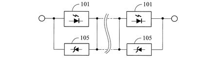
図2に、従来のLED装置であって、2個の発光素子セットを逆極になるように直列接続することによって構成されたLED装置の模式図を示す。
図2に、1個のLEDと1個のツェナーダイオードとを並列接続することにより発光素子ユニットを構成し、2個以上の発光素子ユニットを同極になるように直列接続することにより発光素子セットを構成し、2個以上の発光素子セットを逆方向に直列接続することにより従来のLED装置を構成することを示す。
FIG. 2 is a schematic diagram of a conventional LED device that is configured by connecting two light emitting element sets in series so as to have opposite polarities.
In FIG. 2, a light emitting element unit is configured by connecting one LED and one zener diode in parallel, and two or more light emitting element units are connected in series so as to have the same polarity. It shows that the conventional LED device is configured by connecting two or more light emitting element sets in series in the reverse direction.
(第1実施形態)
図3に、本発明の第1実施形態によるLED装置であって、2個以上の同極性直列接続式LEDセットの両端に1個の共用の電圧制限素子を並列接続するとともに、各LEDの両端に均圧抵抗を並列接続することによって発光素子ユニットを構成するLED装置の模式図を示す。
図3の主な構成は下記を含む。
LED(101)は、発光ダイオードによって構成されている。
電圧制限素子(105)は、過電圧となったときインピーダンスが速やかに下降する半導体素子、例えばツェナーダイオードまたはバリスタによって構成されている。
均圧抵抗(107)は、電阻性素子によって構成され、各LEDの両端と並列接続する。
2個以上のLED(101)を同極になるように直列接続した両端に、1個の共用の電圧制限素子(105)を並列接続するとともに、各LED(101)の両端に均圧抵抗(107)を並列接続することによって、発光素子ユニットを構成する。
(First embodiment)
FIG. 3 shows an LED device according to the first embodiment of the present invention, in which one common voltage limiting element is connected in parallel to both ends of two or more same-polarity series-connected LED sets, and both ends of each LED are connected. The schematic diagram of the LED apparatus which comprises a light emitting element unit by connecting a voltage equalizing resistance in parallel is shown.
The main configuration of FIG.
The LED (101) is composed of a light emitting diode.
The voltage limiting element (105) is configured by a semiconductor element, for example, a Zener diode or a varistor, whose impedance decreases rapidly when an overvoltage occurs.
The voltage equalizing resistor (107) is constituted by an electric blocking element and is connected in parallel with both ends of each LED.
A common voltage limiting element (105) is connected in parallel to both ends of two or more LEDs (101) connected in series so as to have the same polarity, and a voltage equalizing resistance ( 107) are connected in parallel to form a light emitting element unit.
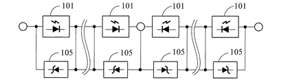
(第2実施形態)
図4に、本発明の第2実施形態によるLED装置であって、図3に示す発光素子ユニットの複数個を同極になるように直列接続または直列・並列接続することによって、発光素子セットを構成するLED装置の模式図を示す。
図4の主な構成は下記を含む。
LED(101)は、発光ダイオードによって構成されている。
電圧制限素子(105)は、過電圧となったときインピーダンスが速やかに下降する半導体素子、例えばツェナーダイオードまたはバリスタによって構成されている。
均圧抵抗(107)は、電阻性素子によって構成され、各LEDの両端と並列接続する。
2個以上のLED(101)を同極になるように直列接続した両端に、1個の共用の電圧制限素子(105)を並列接続するとともに、各LED(101)の両端に均圧抵抗(107)を並列接続することによって、発光素子ユニットを構成する。
複数個の発光素子ユニットを同極になるように直列接続または直列・並列接続することによって、発光素子セットを構成する。
(Second Embodiment)
FIG. 4 shows an LED device according to the second embodiment of the present invention, in which a plurality of light emitting element units shown in FIG. 3 are connected in series or in series / parallel so as to have the same polarity. The schematic diagram of the LED device to comprise is shown.
The main configuration of FIG.
The LED (101) is composed of a light emitting diode.
The voltage limiting element (105) is configured by a semiconductor element, for example, a Zener diode or a varistor, whose impedance decreases rapidly when an overvoltage occurs.
The voltage equalizing resistor (107) is constituted by an electric blocking element and is connected in parallel with both ends of each LED.
A common voltage limiting element (105) is connected in parallel to both ends of two or more LEDs (101) connected in series so as to have the same polarity, and a voltage equalizing resistance ( 107) are connected in parallel to form a light emitting element unit.
A light emitting element set is configured by connecting a plurality of light emitting element units in series or in series / parallel so as to have the same polarity.
(第3実施形態)
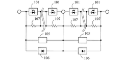
図5に、本発明の第3実施形態によるLED装置であって、図3に示す発光素子ユニットの複数個を逆極になるように直列接続するLED装置の模式図を示す。
図5の主な構成は下記を含む。
LED(101)は、発光ダイオードによって構成されている。
電圧制限素子(105)は、過電圧となったときインピーダンスが速やかに下降する半導体素子、例えばツェナーダイオードまたはバリスタによって構成されている。
均圧抵抗(107)は、電阻性素子によって構成され、各LEDの両端と並列接続する。
2個以上のLED(101)を同極になるように直列接続した両端に、1個の共用の電圧制限素子(105)を並列接続するとともに、各LED(101)の両端に均圧抵抗(107)を並列接続することによって、発光素子ユニットを構成する。
2個の発光素子ユニットは、逆極になるように直列接続されている。
(Third embodiment)
FIG. 5 is a schematic diagram of an LED device according to a third embodiment of the present invention, in which a plurality of the light emitting element units shown in FIG. 3 are connected in series so as to have opposite polarities.
The main configuration of FIG.
The LED (101) is composed of a light emitting diode.
The voltage limiting element (105) is configured by a semiconductor element, for example, a Zener diode or a varistor, whose impedance decreases rapidly when an overvoltage occurs.
The voltage equalizing resistor (107) is constituted by an electric blocking element and is connected in parallel with both ends of each LED.
A common voltage limiting element (105) is connected in parallel to both ends of two or more LEDs (101) connected in series so as to have the same polarity, and a voltage equalizing resistance ( 107) are connected in parallel to form a light emitting element unit.
The two light emitting element units are connected in series so as to have opposite polarities.
(第4実施形態)
図6に、本発明の第4実施形態によるLED装置であって、図4に示す発光素子セットの複数個を逆極になるように直列接続するLED装置の模式図を示す。
図6の主な構成は下記を含む。
LED(101)は、発光ダイオードによって構成されている。
電圧制限素子(105)は、過電圧となったときインピーダンスが速やかに下降する半導体素子、例えばツェナーダイオードまたはバリスタによって構成されている。
均圧抵抗(107)は、電阻性素子によって構成され、各LEDの両端と並列接続する。
2個以上のLED(101)を同極になるように直列接続した両端に、1個の共用の電圧制限素子(105)を並列接続するとともに、各LED(101)の両端に均圧抵抗(107)を並列接続することによって、発光素子ユニットを構成する。
複数個の発光素子ユニットを同極になるように直列接続または直列・並列接続することによって、発光素子セットを構成する。
2個以上の発光素子セットは、逆極になるように直列接続されている。
(Fourth embodiment)
FIG. 6 is a schematic diagram of an LED device according to a fourth embodiment of the present invention, in which a plurality of light emitting element sets shown in FIG. 4 are connected in series so as to have opposite polarities.
The main configuration of FIG. 6 includes the following.
The LED (101) is composed of a light emitting diode.
The voltage limiting element (105) is configured by a semiconductor element, for example, a Zener diode or a varistor, whose impedance decreases rapidly when an overvoltage occurs.
The voltage equalizing resistor (107) is constituted by an electric blocking element and is connected in parallel with both ends of each LED.
A common voltage limiting element (105) is connected in parallel to both ends of two or more LEDs (101) connected in series so as to have the same polarity, and a voltage equalizing resistance ( 107) are connected in parallel to form a light emitting element unit.
A light emitting element set is configured by connecting a plurality of light emitting element units in series or in series / parallel so as to have the same polarity.
Two or more light emitting element sets are connected in series so as to have opposite polarities.
(第5実施形態)
図7に、本発明の第5実施形態によるLED装置であって、図5に示す両発光素子ユニットの両端に別々に接続する逆極性並列接続式ダイオードを備えるLED装置の模式図を示す。
図7の主な構成は下記を含む。
LED(101)は、発光ダイオードによって構成されている。
電圧制限素子(105)は、過電圧となったときインピーダンスが速やかに下降する半導体素子、例えばツェナーダイオードまたはバリスタによって構成されている。
均圧抵抗(107)は、電阻性素子によって構成され、各LEDの両端と並列接続する。
2個以上のLED(101)を同極になるように直列接続した両端に、1個の共用の電圧制限素子(105)を並列接続するとともに、各LED(101)の両端に均圧抵抗(107)を並列接続することによって、発光素子ユニットを構成する。
2個の発光素子ユニットは、逆極になるように直列接続されている。
逆極性並列接続式ダイオード(106)は、発光素子ユニットの両端に別々に接続されている。
(Fifth embodiment)
FIG. 7 is a schematic diagram of an LED device according to a fifth embodiment of the present invention, which includes reverse-polarity parallel-connected diodes that are separately connected to both ends of both light-emitting element units shown in FIG.
The main configuration of FIG.
The LED (101) is composed of a light emitting diode.
The voltage limiting element (105) is configured by a semiconductor element, for example, a Zener diode or a varistor, whose impedance decreases rapidly when an overvoltage occurs.
The voltage equalizing resistor (107) is constituted by an electric blocking element and is connected in parallel with both ends of each LED.
A common voltage limiting element (105) is connected in parallel to both ends of two or more LEDs (101) connected in series so as to have the same polarity, and a voltage equalizing resistance ( 107) are connected in parallel to form a light emitting element unit.
The two light emitting element units are connected in series so as to have opposite polarities.
The reverse polarity parallel connection type diode (106) is separately connected to both ends of the light emitting element unit.
(第6実施形態)
図8に、本発明の第6実施形態によるLED装置であって、図6に示す逆極になるように直列接続された2個以上の発光素子セットのうち、同極になるように直列接続された複数個の発光素子セットの両端に別々に接続された逆極性並列接続式ダイオードを備えるLED装置の模式図を示す。
図8の主な構成は下記を含む。
LED(101)は、発光ダイオードによって構成されている。
電圧制限素子(105)は、過電圧となったときインピーダンスが速やかに下降する半導体素子、例えばツェナーダイオードまたはバリスタによって構成されている。
均圧抵抗(107)は、電阻性素子によって構成され、各LEDの両端と並列接続する。
2個以上のLED(101)を同極になるように直列接続する両端に、1個の共用の電圧制限素子(105)を並列接続するとともに、各LED(101)の両端に均圧抵抗(107)を並列接続することによって、発光素子ユニットを構成する。
複数個の発光素子ユニットを同極になるように直列接続または直列・並列接続することによって、発光素子セットを構成する。
2個以上の発光素子セットは、逆極になるように直列接続されている。
逆極性並列接続式ダイオード(106)は、逆極になるように直列接続された2個以上の発光素子セットのうち、同極になるように直列接続または直列・並列接続された複数個の発光素子セットの両端に別々に接続されている。
(Sixth embodiment)
FIG. 8 shows an LED device according to a sixth embodiment of the present invention, in which two or more light emitting element sets connected in series so as to have the opposite polarity shown in FIG. 6 are connected in series so as to have the same polarity. The schematic diagram of an LED apparatus provided with the reverse polarity parallel connection type diode separately connected to the both ends of the several light emitting element set which were made is shown.
The main configuration of FIG.
The LED (101) is composed of a light emitting diode.
The voltage limiting element (105) is configured by a semiconductor element, for example, a Zener diode or a varistor, whose impedance decreases rapidly when an overvoltage occurs.
The voltage equalizing resistor (107) is constituted by an electric blocking element and is connected in parallel with both ends of each LED.
A common voltage limiting element (105) is connected in parallel to both ends of two or more LEDs (101) connected in series so as to have the same polarity, and a voltage equalizing resistor ( 107) are connected in parallel to form a light emitting element unit.
A light emitting element set is configured by connecting a plurality of light emitting element units in series or in series / parallel so as to have the same polarity.
Two or more light emitting element sets are connected in series so as to have opposite polarities.
The reverse polarity parallel connection type diode (106) is a plurality of light emitting elements connected in series or in series / parallel so as to have the same polarity among two or more light emitting element sets connected in series so as to have opposite polarities. Separately connected to both ends of the element set.
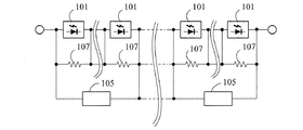
(第7実施形態)
図9に、本発明の第7実施形態によるLED装置であって、2個以上のLEDと電圧制限素子および均圧抵抗とを並列接続することにより構成された発光素子ユニットを、同極になるように直列接続または直列・並列接続することによって発光素子セットを構成するLED装置の模式図を示す。
図9の主な構成は下記を含む。
LED(101)は、発光ダイオードによって構成されている。
電圧制限素子(105)は、過電圧となったときインピーダンスが速やかに下降する半導体素子、例えばツェナーダイオードまたはバリスタによって構成されている。
均圧抵抗(107)は、電阻性素子によって構成され、LEDの両端に並列接続されている。
LEDと電圧制限素子および均圧抵抗とを並列接続することによって、発光素子ユニットを構成する。
2個以上の発光素子ユニットを同極になるように直列接続または直列・並列接続することによって、発光素子セットを構成する。
(Seventh embodiment)
FIG. 9 shows an LED device according to a seventh embodiment of the present invention, wherein a light emitting element unit configured by connecting two or more LEDs, a voltage limiting element and a voltage equalizing resistor in parallel has the same polarity. The schematic diagram of the LED device which comprises a light emitting element set by connecting in series or connecting in series and parallel is shown.
The main configuration of FIG. 9 includes the following.
The LED (101) is composed of a light emitting diode.
The voltage limiting element (105) is configured by a semiconductor element, for example, a Zener diode or a varistor, whose impedance decreases rapidly when an overvoltage occurs.
The voltage equalizing resistor (107) is formed of an electric blocking element and is connected in parallel to both ends of the LED.
A light emitting element unit is configured by connecting an LED, a voltage limiting element, and a voltage equalizing resistor in parallel.
A light emitting element set is configured by connecting two or more light emitting element units in series or in series / parallel so as to have the same polarity.
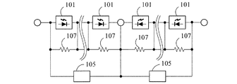
(第8実施形態)
図10に、本発明の第8実施形態によるLED装置であって、図9に示す発光素子セットの2個を逆極になるように直列接続するLED装置の模式図を示す。
図10の主な構成は下記を含む。
LED(101)は、発光ダイオードによって構成されている。
電圧制限素子(105)は、過電圧となったときインピーダンスが速やかに下降する半導体素子、例えばツェナーダイオードまたはバリスタによって構成されている。
均圧抵抗(107)は、電阻性素子によって構成され、LEDの両端と並列接続している。
LEDと電圧制限素子および均圧抵抗とを並列接続することによって、発光素子ユニットを構成する。
2個以上の発光素子ユニットを同極になるように直列接続または直列・並列接続することによって、発光素子セットを構成する。
2個以上の発光素子セットは、逆極になるように直列接続されている。
(Eighth embodiment)
FIG. 10 is a schematic diagram of an LED device according to an eighth embodiment of the present invention, in which two of the light emitting element sets shown in FIG. 9 are connected in series so as to have opposite polarities.
The main configuration of FIG. 10 includes the following.
The LED (101) is composed of a light emitting diode.
The voltage limiting element (105) is configured by a semiconductor element, for example, a Zener diode or a varistor, whose impedance decreases rapidly when an overvoltage occurs.
The voltage equalizing resistor (107) is constituted by an electric blocking element, and is connected in parallel with both ends of the LED.
A light emitting element unit is configured by connecting an LED, a voltage limiting element, and a voltage equalizing resistor in parallel.
A light emitting element set is configured by connecting two or more light emitting element units in series or in series / parallel so as to have the same polarity.
Two or more light emitting element sets are connected in series so as to have opposite polarities.
上述の実施形態によるLED装置の電源は、定電流電源、定電圧電源、電流電源制限、限圧電源または電流または電圧の制御が行われていない電源を用いることができる。ただし本発明の電圧制限素子の稼働に合わせて、電源出力側の本体の中にあるインピーダンス、または電源出力端と負荷との間にインピーダンス素子を連続設置することによって、電源や電圧が変動するとき、電圧制限素子を流れる電流を通して、インピーダンス素子の両端で電圧降下を変化させることにより、LED装置の両端の電圧を調節する。 As a power source of the LED device according to the above-described embodiment, a constant current power source, a constant voltage power source, a current power source limit, a limited voltage power source, or a power source that is not controlled in current or voltage can be used. However, when the power supply or voltage fluctuates by continuously installing the impedance element in the main body on the power supply output side or between the power supply output terminal and the load in accordance with the operation of the voltage limiting element of the present invention The voltage across the LED device is adjusted by changing the voltage drop across the impedance element through the current flowing through the voltage limiting element.
(他の実施形態)
本発明の他の実施形態では、LED(101)は、1個の発光ダイオードから構成されるか場合のみならず、互いに直列接続または並列接続または直列・並列接続された複数個の発光ダイオードからなるLEDユニットから構成されてもよい。
(Other embodiments)
In another embodiment of the present invention, the LED (101) is not only composed of one light emitting diode, but also composed of a plurality of light emitting diodes connected in series or in parallel or in series and parallel. You may comprise from an LED unit.
本発明の他の実施形態では、電圧制限素子(105)は、ツェナーダイオード、バリスタ、順方向電圧降下を持つダイオード、および、逆極性順方向電圧降下を持つツェナーダイオードのうち1個から構成されること、および、ツェナーダイオード、バリスタ、順方向電圧降下を持つダイオード、および、逆極性順方向電圧降下を持つツェナーダイオードのうち少なくとも一種以上であり且つ複数個の素子が互いに同極になるように直列接続または並列接続または直列・並列接続されてなる素子ユニットから構成されることを含む。 In another embodiment of the present invention, the voltage limiting element (105) is composed of one of a Zener diode, a varistor, a diode having a forward voltage drop, and a Zener diode having a reverse polarity forward voltage drop. And at least one of a Zener diode, a varistor, a diode having a forward voltage drop, and a Zener diode having a reverse polarity forward voltage drop, and a plurality of elements having the same polarity. It is comprised from the element unit formed by connection, parallel connection, or series and parallel connection.
101・・・LED
105・・・電圧制限素子
106・・・ダイオード
107・・・均圧抵抗
101 ... LED
105 ...
Claims (10)
前記LED(101)は発光ダイオードによって構成され、
前記電圧制限素子(105)は、過電圧となったときインピーダンスが速やかに下降する半導体素子によって構成され、
前記均圧抵抗(107)は、電阻性素子によって構成され、各前記LEDの両端に並列接続され、
前記発光素子ユニットは、2個以上の前記LED(101)を同極になるように直列接続した両端に、1個の共用の前記電圧制限素子(105)を並列接続するとともに、各前記LED(101)の両端に前記均圧抵抗(107)を並列接続することによって構成されていることを特徴とするLED装置。 An LED device having a light emitting element unit configured by connecting a common voltage limiting element in parallel to both ends of two or more same-polarity series-connected LED sets and connecting a voltage equalizing resistor in parallel to both ends of each LED There,
The LED (101) is constituted by a light emitting diode,
The voltage limiting element (105) is constituted by a semiconductor element whose impedance decreases rapidly when an overvoltage occurs.
The voltage equalizing resistor (107) is constituted by an electric blocking element, and is connected in parallel to both ends of each LED,
The light emitting element unit is configured such that one voltage limiting element (105) is connected in parallel to both ends of two or more LEDs (101) connected in series so as to have the same polarity, and each LED ( 101), and the equalizing resistor (107) is connected in parallel to both ends of the LED device.
前記電圧制限素子(105)は、過電圧となったときインピーダンスが速やかに下降する半導体素子によって構成され、
前記均圧抵抗(107)は、電阻性素子によって構成され、各前記LEDの両端に並列接続され、
前記発光素子ユニットは、2個以上の前記LED(101)を同極になるように直列接続した両端に、1個の共用の前記電圧制限素子(105)を並列接続するとともに、各前記LED(101)の両端に前記均圧抵抗(107)を並列接続することによって構成され、
複数個の前記発光素子ユニットを同極になるように直列接続または直列・並列接続することによって構成された発光素子セットを有することを特徴とする請求項1に記載のLED装置。 The LED (101) is constituted by a light emitting diode,
The voltage limiting element (105) is constituted by a semiconductor element whose impedance decreases rapidly when an overvoltage occurs.
The voltage equalizing resistor (107) is constituted by an electric blocking element, and is connected in parallel to both ends of each LED,
The light emitting element unit is configured such that one voltage limiting element (105) is connected in parallel to both ends of two or more LEDs (101) connected in series so as to have the same polarity, and each LED ( 101) by connecting the equalizing resistor (107) in parallel to both ends,
2. The LED device according to claim 1, further comprising: a light emitting element set configured by connecting a plurality of the light emitting element units in series or in series / parallel so as to have the same polarity.
前記電圧制限素子(105)は、過電圧となったときインピーダンスが速やかに下降する半導体素子によって構成され、
前記均圧抵抗(107)は、電阻性素子によって構成され、各前記LEDの両端に並列接続され、
前記発光素子ユニットは、2個以上の前記LED(101)を同極になるように直列接続した両端に、1個の共用の前記電圧制限素子(105)を並列接続するとともに、各前記LED(101)の両端に前記均圧抵抗(107)を並列接続することによって構成され、
2個の前記発光素子ユニットは、互いに逆極になるように直列接続されていることを特徴とする請求項1に記載のLED装置。 The LED (101) is constituted by a light emitting diode,
The voltage limiting element (105) is constituted by a semiconductor element whose impedance decreases rapidly when an overvoltage occurs.
The voltage equalizing resistor (107) is constituted by an electric blocking element, and is connected in parallel to both ends of each LED,
The light emitting element unit is configured such that one voltage limiting element (105) is connected in parallel to both ends of two or more LEDs (101) connected in series so as to have the same polarity, and each LED ( 101) by connecting the equalizing resistor (107) in parallel to both ends,
The LED device according to claim 1, wherein the two light emitting element units are connected in series so as to have opposite polarities.
前記電圧制限素子(105)は、過電圧となったときインピーダンスが速やかに下降する半導体素子によって構成され、
前記均圧抵抗(107)は、電阻性素子によって構成され、各前記LEDの両端に並列接続され、
前記発光素子ユニットは、2個以上の前記LED(101)を同極になるように直列接続した両端に、1個の共用の前記電圧制限素子(105)を並列接続するとともに、各前記LED(101)の両端に前記均圧抵抗(107)を並列接続することによって構成され、
前記発光素子セットは、複数個の前記発光素子ユニットを同極になるように直列接続または直列・並列接続することによって構成され、
2個以上の前記発光素子セットは、互いに逆極になるように直列接続されていることを特徴とする請求項2に記載のLED装置。 The LED (101) is constituted by a light emitting diode,
The voltage limiting element (105) is constituted by a semiconductor element whose impedance decreases rapidly when an overvoltage occurs.
The voltage equalizing resistor (107) is constituted by an electric blocking element, and is connected in parallel to both ends of each LED,
The light emitting element unit is configured such that one voltage limiting element (105) is connected in parallel to both ends of two or more LEDs (101) connected in series so as to have the same polarity, and each LED ( 101) by connecting the equalizing resistor (107) in parallel to both ends,
The light emitting element set is configured by connecting a plurality of the light emitting element units in series or in series / parallel so as to have the same polarity,
The LED device according to claim 2, wherein the two or more light emitting element sets are connected in series so as to have opposite polarities.
前記電圧制限素子(105)は、過電圧となったときインピーダンスが速やかに下降する半導体素子によって構成され、
前記均圧抵抗(107)は、電阻性素子によって構成され、各前記LEDの両端に並列接続され、
前記発光素子ユニットは、2個以上の前記LED(101)を同極になるように直列接続した両端に、1個の共用の前記電圧制限素子(105)を並列接続するとともに、各前記LED(101)の両端に前記均圧抵抗(107)を並列接続することによって構成され、
2個の前記発光素子ユニットは、互いに逆極になるように直列接続され、
2個の前記発光素子ユニットの両端に別々に接続する逆極性並列接続式ダイオード(106)をさらに備えていることを特徴とする請求項3に記載のLED装置。 The LED (101) is constituted by a light emitting diode,
The voltage limiting element (105) is constituted by a semiconductor element whose impedance decreases rapidly when an overvoltage occurs.
The voltage equalizing resistor (107) is constituted by an electric blocking element, and is connected in parallel to both ends of each LED,
The light emitting element unit is configured such that one voltage limiting element (105) is connected in parallel to both ends of two or more LEDs (101) connected in series so as to have the same polarity, and each LED ( 101) by connecting the equalizing resistor (107) in parallel to both ends,
The two light emitting element units are connected in series so as to have opposite polarities,
The LED device according to claim 3, further comprising reverse-polarity parallel-connected diodes (106) connected separately to both ends of the two light-emitting element units.
前記電圧制限素子(105)は、過電圧となったときインピーダンスが速やかに下降する半導体素子によって構成され、
前記均圧抵抗(107)は、電阻性素子によって構成され、各前記LEDの両端に並列接続され、
前記発光素子ユニットは、2個以上の前記LED(101)を同極になるように直列接続した両端に、1個の共用の前記電圧制限素子(105)を並列接続するとともに、各前記LED(101)の両端に前記均圧抵抗(107)を並列接続することによって構成され、
前記発光素子セットは、複数個の前記発光素子ユニットを同極になるように直列接続または直列・並列接続することによって構成され、
2個以上の前記発光素子セットは、互いに逆極になるように直列接続され、
逆極になるように直列接続された2個以上の前記発光素子セットのうち、同極になるように直列接続または直列・並列接続された1個または複数個の前記発光素子セットの両端に別々に接続する逆極性並列接続式ダイオード(106)をさらに備えていることを特徴とする請求項4に記載のLED装置。 The LED (101) is constituted by a light emitting diode,
The voltage limiting element (105) is constituted by a semiconductor element whose impedance decreases rapidly when an overvoltage occurs.
The voltage equalizing resistor (107) is constituted by an electric blocking element, and is connected in parallel to both ends of each LED,
The light emitting element unit is configured such that one voltage limiting element (105) is connected in parallel to both ends of two or more LEDs (101) connected in series so as to have the same polarity, and each LED ( 101) by connecting the equalizing resistor (107) in parallel to both ends,
The light emitting element set is configured by connecting a plurality of the light emitting element units in series or in series / parallel so as to have the same polarity,
The two or more light emitting element sets are connected in series so as to have opposite polarities,
Out of two or more light emitting element sets connected in series so as to have opposite poles, one or more of the light emitting element sets connected in series or connected in series / parallel so as to have the same polarity are separately provided at both ends. The LED device according to claim 4, further comprising a reverse-polarity parallel-connected diode (106) connected to the LED.
前記電圧制限素子(105)は、過電圧となったときインピーダンスが速やかに下降する半導体素子によって構成され、
前記均圧抵抗(107)は、電阻性素子によって構成され、各前記LEDの両端に並列接続され、
前記発光素子ユニットは、前記LEDの両端に前記電圧制限素子および前記均圧抵抗を並列接続することによって構成され、
2個以上の前記発光素子ユニットを同極になるように直列接続または直列・並列接続することによって構成された発光素子セットを有することを特徴とする請求項1に記載のLED装置。 The LED (101) is constituted by a light emitting diode,
The voltage limiting element (105) is constituted by a semiconductor element whose impedance decreases rapidly when an overvoltage occurs.
The voltage equalizing resistor (107) is constituted by an electric blocking element, and is connected in parallel to both ends of each LED,
The light emitting element unit is configured by connecting the voltage limiting element and the voltage equalizing resistor in parallel to both ends of the LED,
2. The LED device according to claim 1, comprising a light emitting element set configured by connecting two or more light emitting element units in series or in series / parallel so as to have the same polarity.
前記電圧制限素子(105)は、過電圧となったときインピーダンスが速やかに下降する半導体素子によって構成され、
前記均圧抵抗(107)は、電阻性素子によって構成され、各前記LEDの両端に並列接続され、
前記発光素子ユニットは、前記LEDの両端に前記電圧制限素子および前記均圧抵抗を並列接続することによって構成され、
前記発光素子セットは、2個以上の前記発光素子ユニットを同極になるように直列接続または直列・並列接続することによって構成され、
2個以上の前記発光素子セットは、互いに逆極になるように直列接続されていることを特徴とする請求項7に記載のLED装置。 The LED (101) is constituted by a light emitting diode,
The voltage limiting element (105) is constituted by a semiconductor element whose impedance decreases rapidly when an overvoltage occurs.
The voltage equalizing resistor (107) is constituted by an electric blocking element, and is connected in parallel to both ends of each LED,
The light emitting element unit is configured by connecting the voltage limiting element and the voltage equalizing resistor in parallel to both ends of the LED,
The light emitting element set is configured by connecting two or more light emitting element units in series or in series and parallel so as to have the same polarity,
The LED device according to claim 7, wherein the two or more light emitting element sets are connected in series so as to have opposite polarities.
Applications Claiming Priority (4)
| Application Number | Priority Date | Filing Date | Title |
|---|---|---|---|
| US13/025,284 US8823269B2 (en) | 2011-02-11 | 2011-02-11 | LED device with shared voltage-limiting unit and individual equalizing resistance |
| US13/025,320 | 2011-02-11 | ||
| US13/025,284 | 2011-02-11 | ||
| US13/025,320 US8624508B2 (en) | 2011-02-11 | 2011-02-11 | LED device with voltage-limiting unit and voltage-equalizing resistance |
Related Child Applications (1)
| Application Number | Title | Priority Date | Filing Date |
|---|---|---|---|
| JP2019111708A Division JP2019195075A (en) | 2011-02-11 | 2019-06-17 | LED device |
Publications (2)
| Publication Number | Publication Date |
|---|---|
| JP2012169625A true JP2012169625A (en) | 2012-09-06 |
| JP2012169625A5 JP2012169625A5 (en) | 2016-04-14 |
Family
ID=45655540
Family Applications (2)
| Application Number | Title | Priority Date | Filing Date |
|---|---|---|---|
| JP2012027982A Pending JP2012169625A (en) | 2011-02-11 | 2012-02-13 | Led device |
| JP2019111708A Pending JP2019195075A (en) | 2011-02-11 | 2019-06-17 | LED device |
Family Applications After (1)
| Application Number | Title | Priority Date | Filing Date |
|---|---|---|---|
| JP2019111708A Pending JP2019195075A (en) | 2011-02-11 | 2019-06-17 | LED device |
Country Status (5)
| Country | Link |
|---|---|
| EP (1) | EP2487993B1 (en) |
| JP (2) | JP2012169625A (en) |
| CN (2) | CN202513156U (en) |
| SG (1) | SG183625A1 (en) |
| TW (2) | TWI583243B (en) |
Cited By (2)
| Publication number | Priority date | Publication date | Assignee | Title |
|---|---|---|---|---|
| KR101535790B1 (en) * | 2014-07-15 | 2015-07-13 | (주)로그인디지탈 | Circuit board for LED lighting with protection means |
| JP7440196B2 (en) | 2022-04-08 | 2024-02-28 | 株式会社スリーエス | LED device |
Families Citing this family (8)
| Publication number | Priority date | Publication date | Assignee | Title |
|---|---|---|---|---|
| SG183625A1 (en) * | 2011-02-11 | 2012-09-27 | Tai-Her Yang | Led device with shared voltage-limiting unit and individual voltage-equalizing resistance |
| CN104061467A (en) * | 2014-03-31 | 2014-09-24 | 中山市新邦照明电器有限公司 | Novel LED lamp |
| WO2015174877A2 (en) * | 2014-05-15 | 2015-11-19 | Rus Adrian Ioan | Direct ac led driver flicker index reduction circuit and method |
| IT201700010434A1 (en) * | 2017-01-31 | 2018-07-31 | Oec S R L | TERMINAL BOARD FOR LIGHTING SYSTEMS. |
| CN110417285A (en) * | 2019-06-30 | 2019-11-05 | 武汉东城新能源有限公司 | A kind of novel high-frequency high voltage silicon rectifier stack circuit |
| US11411492B1 (en) | 2021-05-29 | 2022-08-09 | Nxp B.V. | Self limiting charge pump |
| US11321600B1 (en) | 2021-05-29 | 2022-05-03 | Nxp B.V. | RFID tag self tuning |
| US11556751B2 (en) | 2021-05-29 | 2023-01-17 | Nxp B.V. | RFID tag limiter |
Citations (10)
| Publication number | Priority date | Publication date | Assignee | Title |
|---|---|---|---|---|
| JPS5684368U (en) * | 1979-11-29 | 1981-07-07 | ||
| JPS57167690A (en) * | 1981-04-07 | 1982-10-15 | Toa Tokushu Denki Kk | Control of light-emitting diode |
| US20020043943A1 (en) * | 2000-10-10 | 2002-04-18 | Menzer Randy L. | LED array primary display light sources employing dynamically switchable bypass circuitry |
| JP2004512697A (en) * | 2000-10-24 | 2004-04-22 | ゼネラル・エレクトリック・カンパニイ | LED power supply |
| JP2004340830A (en) * | 2003-05-16 | 2004-12-02 | Calsonic Kansei Corp | Lighting system and display for vehicle having the same |
| JP2007165161A (en) * | 2005-12-15 | 2007-06-28 | Sharp Corp | Led illumination device, led backlight device, and image display device |
| WO2008101383A1 (en) * | 2007-02-17 | 2008-08-28 | Shenzhen Unibero Technology Co., Ltd | Led lamp assembly, series circuit of led lamp assembly and led lighting device |
| JP2009301952A (en) * | 2008-06-16 | 2009-12-24 | Showa Denko Kk | Light-emitting device and lighting system equipped therewith |
| JP3157456U (en) * | 2009-12-02 | 2010-02-18 | 黄泰翔 | Protection circuit for AC LED |
| WO2010073437A1 (en) * | 2008-12-26 | 2010-07-01 | 三菱電機株式会社 | Led operation device and head lamp led operation device |
Family Cites Families (15)
| Publication number | Priority date | Publication date | Assignee | Title |
|---|---|---|---|---|
| DE4434274A1 (en) * | 1994-09-24 | 1996-03-28 | Blaupunkt Werke Gmbh | Lighting arrangement with light-emitting diodes connected in series |
| US5575459A (en) * | 1995-04-27 | 1996-11-19 | Uniglo Canada Inc. | Light emitting diode lamp |
| US6323598B1 (en) * | 2000-09-29 | 2001-11-27 | Aerospace Optics, Inc. | Enhanced trim resolution voltage-controlled dimming led driver |
| US7262752B2 (en) * | 2001-01-16 | 2007-08-28 | Visteon Global Technologies, Inc. | Series led backlight control circuit |
| US6628085B2 (en) * | 2001-01-17 | 2003-09-30 | Tai-Her Yang | Limit voltage circuit using light emitting diodes as thermal-loss reducing impedances, especially for matching a saturation voltage of rechargeable cells during charging |
| FR2891106A1 (en) * | 2005-09-20 | 2007-03-23 | Patrick Courteix | LEDs supplying and connecting method for producing lamp e.g. automobile lamp, involves connecting LEDs in series and associating Zener diode in parallel on each LED, where diode presents Zener voltage value greater than LED voltage |
| FR2897574A1 (en) * | 2006-02-17 | 2007-08-24 | Valeo Vision Sa | LED circuit for lighting/signaling device, has flat power cable of LEDs including bared part connected to general power cable to ensure electrical connection, and another set of bared parts with two ends of two wires soldered on LED module |
| JP2008131007A (en) * | 2006-11-24 | 2008-06-05 | Koha Co Ltd | Light-emitting circuit and lighting device having the same |
| EP2172082B1 (en) * | 2007-06-19 | 2020-10-14 | Silicon Line GmbH | Circuit arrangement and method for controlling light-emitting components |
| TW200939884A (en) * | 2008-03-07 | 2009-09-16 | Tai-Her Yang | Unipolar (dis) charging LED drive method and circuit thereof |
| US8054004B2 (en) * | 2008-03-07 | 2011-11-08 | Tai-Her Yang | Bipolar (dis)charging LED drive method and circuit thereof |
| US20100315014A1 (en) * | 2009-06-16 | 2010-12-16 | Cheng-Fen Chang | LED light string |
| TWM379169U (en) * | 2009-11-09 | 2010-04-21 | Tai-Hsiang Huang | Protection device of alternating light-emitting diode driving circuit |
| CN201557282U (en) * | 2009-11-17 | 2010-08-18 | 黄泰翔 | LED (light emitting diode)protection circuit for alternating current use |
| SG183625A1 (en) * | 2011-02-11 | 2012-09-27 | Tai-Her Yang | Led device with shared voltage-limiting unit and individual voltage-equalizing resistance |
-
2012
- 2012-02-08 SG SG2012008926A patent/SG183625A1/en unknown
- 2012-02-09 CN CN2012200422989U patent/CN202513156U/en not_active Expired - Lifetime
- 2012-02-09 EP EP20120154750 patent/EP2487993B1/en not_active Not-in-force
- 2012-02-09 TW TW101104143A patent/TWI583243B/en active
- 2012-02-09 CN CN201210028981.1A patent/CN102637683B/en active Active
- 2012-02-09 TW TW101202317U patent/TWM440534U/en unknown
- 2012-02-13 JP JP2012027982A patent/JP2012169625A/en active Pending
-
2019
- 2019-06-17 JP JP2019111708A patent/JP2019195075A/en active Pending
Patent Citations (10)
| Publication number | Priority date | Publication date | Assignee | Title |
|---|---|---|---|---|
| JPS5684368U (en) * | 1979-11-29 | 1981-07-07 | ||
| JPS57167690A (en) * | 1981-04-07 | 1982-10-15 | Toa Tokushu Denki Kk | Control of light-emitting diode |
| US20020043943A1 (en) * | 2000-10-10 | 2002-04-18 | Menzer Randy L. | LED array primary display light sources employing dynamically switchable bypass circuitry |
| JP2004512697A (en) * | 2000-10-24 | 2004-04-22 | ゼネラル・エレクトリック・カンパニイ | LED power supply |
| JP2004340830A (en) * | 2003-05-16 | 2004-12-02 | Calsonic Kansei Corp | Lighting system and display for vehicle having the same |
| JP2007165161A (en) * | 2005-12-15 | 2007-06-28 | Sharp Corp | Led illumination device, led backlight device, and image display device |
| WO2008101383A1 (en) * | 2007-02-17 | 2008-08-28 | Shenzhen Unibero Technology Co., Ltd | Led lamp assembly, series circuit of led lamp assembly and led lighting device |
| JP2009301952A (en) * | 2008-06-16 | 2009-12-24 | Showa Denko Kk | Light-emitting device and lighting system equipped therewith |
| WO2010073437A1 (en) * | 2008-12-26 | 2010-07-01 | 三菱電機株式会社 | Led operation device and head lamp led operation device |
| JP3157456U (en) * | 2009-12-02 | 2010-02-18 | 黄泰翔 | Protection circuit for AC LED |
Cited By (2)
| Publication number | Priority date | Publication date | Assignee | Title |
|---|---|---|---|---|
| KR101535790B1 (en) * | 2014-07-15 | 2015-07-13 | (주)로그인디지탈 | Circuit board for LED lighting with protection means |
| JP7440196B2 (en) | 2022-04-08 | 2024-02-28 | 株式会社スリーエス | LED device |
Also Published As
| Publication number | Publication date |
|---|---|
| SG183625A1 (en) | 2012-09-27 |
| TWM440534U (en) | 2012-11-01 |
| EP2487993B1 (en) | 2015-05-06 |
| CN102637683A (en) | 2012-08-15 |
| JP2019195075A (en) | 2019-11-07 |
| CN102637683B (en) | 2017-04-12 |
| EP2487993A3 (en) | 2013-11-13 |
| CN202513156U (en) | 2012-10-31 |
| TW201240516A (en) | 2012-10-01 |
| EP2487993A2 (en) | 2012-08-15 |
| TWI583243B (en) | 2017-05-11 |
Similar Documents
| Publication | Publication Date | Title |
|---|---|---|
| JP2019195075A (en) | LED device | |
| KR101822192B1 (en) | Voltage-limiting and reverse polarity series type led device | |
| TWI425871B (en) | Apparatus for driving load | |
| JP2012169625A5 (en) | ||
| JP2014096576A (en) | LED Drive circuit | |
| US20110062871A1 (en) | Ac-led protection circuit | |
| KR20110005566A (en) | High efficient constant current circuit for temperature compensation, preventing over-voltage and over-current | |
| US20140132156A1 (en) | Led device with voltage-limiting unit and shunt current-limiting resistance | |
| US9018843B2 (en) | LED device with voltage-limiting unit and voltage-equalizing and current limiting resistances | |
| TW201505310A (en) | Light emitting diode apparatus with over current protection function and system for the same | |
| JP3176177U (en) | LED device | |
| US9282607B2 (en) | LED device with shared voltage-limiting unit and individual equalizing resistance | |
| KR102240099B1 (en) | Led device with shared voltage-limiting unit and individual voltage-equalizing resistance | |
| JP2012178559A (en) | Led device | |
| US20120081004A1 (en) | Light emitting diode system | |
| US9307610B2 (en) | Low power bypass circuit for LED open circuit and reverse polarity protection | |
| US8624508B2 (en) | LED device with voltage-limiting unit and voltage-equalizing resistance | |
| KR20130097410A (en) | Led device with shared voltage-limiting unit and individual voltage-equalizing resistance | |
| KR20130097414A (en) | Led device with voltage-limiting unit and shunt current-limiting resistance | |
| JP5567316B2 (en) | LED lighting device | |
| RU2257654C1 (en) | Voltage surge protective device (alternatives) | |
| KR20160148169A (en) | Driver circuit for LED device |
Legal Events
| Date | Code | Title | Description |
|---|---|---|---|
| A621 | Written request for application examination |
Free format text: JAPANESE INTERMEDIATE CODE: A621 Effective date: 20150106 |
|
| A977 | Report on retrieval |
Free format text: JAPANESE INTERMEDIATE CODE: A971007 Effective date: 20151028 |
|
| A131 | Notification of reasons for refusal |
Free format text: JAPANESE INTERMEDIATE CODE: A131 Effective date: 20151029 |
|
| A601 | Written request for extension of time |
Free format text: JAPANESE INTERMEDIATE CODE: A601 Effective date: 20160129 |
|
| A524 | Written submission of copy of amendment under article 19 pct |
Free format text: JAPANESE INTERMEDIATE CODE: A524 Effective date: 20160229 |
|
| A131 | Notification of reasons for refusal |
Free format text: JAPANESE INTERMEDIATE CODE: A131 Effective date: 20160726 |
|
| A601 | Written request for extension of time |
Free format text: JAPANESE INTERMEDIATE CODE: A601 Effective date: 20161024 |
|
| A601 | Written request for extension of time |
Free format text: JAPANESE INTERMEDIATE CODE: A601 Effective date: 20161223 |
|
| A521 | Request for written amendment filed |
Free format text: JAPANESE INTERMEDIATE CODE: A523 Effective date: 20170111 |
|
| A02 | Decision of refusal |
Free format text: JAPANESE INTERMEDIATE CODE: A02 Effective date: 20170620 |
|
| A521 | Request for written amendment filed |
Free format text: JAPANESE INTERMEDIATE CODE: A523 Effective date: 20171010 |
|
| A521 | Request for written amendment filed |
Free format text: JAPANESE INTERMEDIATE CODE: A821 Effective date: 20171011 |
|
| A911 | Transfer to examiner for re-examination before appeal (zenchi) |
Free format text: JAPANESE INTERMEDIATE CODE: A911 Effective date: 20171110 |
|
| A912 | Re-examination (zenchi) completed and case transferred to appeal board |
Free format text: JAPANESE INTERMEDIATE CODE: A912 Effective date: 20180119 |
|
| A601 | Written request for extension of time |
Free format text: JAPANESE INTERMEDIATE CODE: A601 Effective date: 20181015 |
|
| A601 | Written request for extension of time |
Free format text: JAPANESE INTERMEDIATE CODE: A601 Effective date: 20181119 |
|
| A601 | Written request for extension of time |
Free format text: JAPANESE INTERMEDIATE CODE: A601 Effective date: 20190415 |
|
| A601 | Written request for extension of time |
Free format text: JAPANESE INTERMEDIATE CODE: A601 Effective date: 20190515 |