JP2012165261A - Power amplifier circuit and communication device including this circuit - Google Patents
Power amplifier circuit and communication device including this circuit Download PDFInfo
- Publication number
- JP2012165261A JP2012165261A JP2011025178A JP2011025178A JP2012165261A JP 2012165261 A JP2012165261 A JP 2012165261A JP 2011025178 A JP2011025178 A JP 2011025178A JP 2011025178 A JP2011025178 A JP 2011025178A JP 2012165261 A JP2012165261 A JP 2012165261A
- Authority
- JP
- Japan
- Prior art keywords
- power
- signal
- power amplifier
- cfr
- pulse
- Prior art date
- Legal status (The legal status is an assumption and is not a legal conclusion. Google has not performed a legal analysis and makes no representation as to the accuracy of the status listed.)
- Withdrawn
Links
Images


Abstract
Description
本発明は、CFR(Crest Factor Reduction)機能が付加された包絡線除去・復元(EER)方式の電力増幅回路と、この回路を有する通信装置に関するものである。 The present invention relates to an envelope removal / restoration (EER) type power amplification circuit to which a CFR (Crest Factor Reduction) function is added, and a communication apparatus having this circuit.
例えば、OFDM(Orthogonal Frequency Division Multiplex :直交周波数分割多重)方式やW−CDMA(Wideband Code Division Multiple Access)方式のような、複数の搬送波を用いて送信信号を変調する方式では、搬送波の位相が重なり合って大きなピーク電力を持つ信号になることがある。
その一方で、電力増幅器(パワーアンプ)には優れた線形性が要求されるが、最大出力を超えるレベルの信号が入力されると、出力が飽和して非線形歪みが増大する。
For example, in a method of modulating a transmission signal using a plurality of carriers, such as an OFDM (Orthogonal Frequency Division Multiplex) method and a W-CDMA (Wideband Code Division Multiple Access) method, the phases of the carriers overlap. May have a large peak power.
On the other hand, the power amplifier (power amplifier) is required to have excellent linearity. However, when a signal having a level exceeding the maximum output is input, the output is saturated and nonlinear distortion increases.
このため、大きなピーク電力の信号を非線形増幅器に入力すると出力信号に非線形歪みが生じ、受信側における受信特性の劣化や帯域外輻射の原因となる。
ピーク電力に対して非線形歪みを増大させないためには、ダイナミックレンジの広い電力増幅器が必要となるが、頻繁には出現しないピーク電力のためにダイナミックレンジを広げると、時間軸上の波形の平均電力と短時間のピーク電力との比(PAPR:Peak to Average Power Ratio)が大きくなり、電力効率が悪くなる。
For this reason, when a signal having a large peak power is input to the nonlinear amplifier, nonlinear distortion occurs in the output signal, which causes deterioration of reception characteristics and out-of-band radiation on the reception side.
In order not to increase nonlinear distortion with respect to peak power, a power amplifier with a wide dynamic range is required, but if the dynamic range is widened due to peak power that does not appear frequently, the average power of the waveform on the time axis And the peak power for a short time (PAPR: Peak to Average Power Ratio) are increased, and the power efficiency is deteriorated.
従って、出現頻度が低い大きなピーク電力の信号については、そのまま増幅器に入力するよりも入力前に抑制する方が合理的である。そこで、電力増幅前のIQベースバンド信号のピーク電力を抑制するため、所定の閾値を超えるピーク電力のIQベースバンド信号に対して瞬間的に逆向きの振幅を与えるクリッピング処理を行う場合がある。
この処理は、時間軸上でインパルス状の信号を逆向きに印加する処理であるから、周波数軸上では、広い周波数帯域のノイズが印加されるのと同じこととなる。そのため、クリッピングのみを単純に行った場合には、帯域外にノイズを生じさせるという問題がある。
Therefore, it is more reasonable to suppress a signal having a large peak power with a low appearance frequency before being input to the amplifier as it is. Therefore, in order to suppress the peak power of the IQ baseband signal before power amplification, there is a case where a clipping process is performed in which an IQ baseband signal having a peak power exceeding a predetermined threshold is instantaneously given an opposite amplitude.
Since this process is a process of applying an impulse signal in the reverse direction on the time axis, it is the same as applying noise in a wide frequency band on the frequency axis. For this reason, there is a problem that noise is generated outside the band when only clipping is performed.
そこで、かかる帯域外輻射の問題に対処するため、NS−CFR(Noise Shaping-Crest Factor Reduction)及びPC−CFR(Peak Cancellation - Crest Factor Reduction)と呼ばれるピーク電力抑制回路が知られている。
このうち、NS−CFRは、瞬時電力が閾値を超えるIQベースバンド信号のピーク成分に対して、ローパスフィルタやFIR(Finite Impulse Response )フィルタ等でフィルタリングを行って帯域制限し、この帯域制限後のピーク成分を元のIQベースバンド信号から減算するものである(特許文献1参照)。
Therefore, in order to deal with the problem of out-of-band radiation, peak power suppression circuits called NS-CFR (Noise Shaping-Crest Factor Reduction) and PC-CFR (Peak Cancellation-Crest Factor Reduction) are known.
Among these, NS-CFR performs band limitation by filtering the peak component of the IQ baseband signal whose instantaneous power exceeds the threshold by using a low-pass filter, FIR (Finite Impulse Response) filter, and the like. The peak component is subtracted from the original IQ baseband signal (see Patent Document 1).
また、PC−CFRは、クリッピングしても帯域外輻射を生じさせないための基本関数を予め設定しておき、瞬時電力が閾値を超えるIQベースバンド信号のピーク成分にその基本関数を乗算したものを、元のIQベースバンド信号から減算するものである(特許文献2及び3参照)。
The PC-CFR has a basic function that does not cause out-of-band radiation even when clipping, and is obtained by multiplying the peak component of an IQ baseband signal whose instantaneous power exceeds a threshold by the basic function. Subtract from the original IQ baseband signal (see
一方、パワーアンプのドレイン電圧を入力側の電力に応じて変化させることにより、固定電圧の場合の動作時に生じる電力ロスを減らして高周波増幅器を高効率化する技術として、包絡線除去・復元(Envelope Elimination and Restoration:以下、「EER」という。)方式の電力増幅回路や、包絡線追跡(Envelope Tracking:以下、「ET」という。)方式の電力増幅回路が知られている(特許文献4参照)。 On the other hand, by changing the drain voltage of the power amplifier according to the power on the input side, the power loss that occurs during operation with a fixed voltage is reduced to improve the efficiency of the high-frequency amplifier. Elimination and Restoration (hereinafter referred to as “EER”) type power amplification circuit and envelope tracking (hereinafter referred to as “ET”) type power amplification circuit are known (see Patent Document 4). .
このうち、EER方式では、入力変調信号を位相成分と振幅成分に分離(ポーラ変調)し、位相成分を一定振幅でパワーアンプに入力して常に効率が最大となる飽和付近で動作させる。これに対して、振幅成分は、高効率に電力増幅されて強度変調された電力(変調電源)としてパワーアンプに供給される。
このように動作させることで、パワーアンプが乗算器として動作して位相成分と振幅成分が合成され、バックオフによらない高効率で増幅された出力変調信号が得られる。
Among these, in the EER system, an input modulation signal is separated into a phase component and an amplitude component (polar modulation), and the phase component is input to the power amplifier with a constant amplitude to operate near saturation at which efficiency is always maximized. On the other hand, the amplitude component is supplied to the power amplifier as power (modulated power supply) that has been power amplified and intensity-modulated with high efficiency.
By operating in this way, the power amplifier operates as a multiplier to combine the phase component and the amplitude component, and an output modulation signal amplified with high efficiency without backoff is obtained.
ET方式も、入力変調信号の振幅成分を高効率に電力増幅し、強度変調された電力としてパワーアンプに供給する点は、EER方式と同様である。
両者の違いは、EER方式では、振幅一定の位相変調信号のみをパワーアンプに入力することにより、パワーアンプを飽和動作させるのに対して、ET方式では、振幅成分と位相成分の双方を含む入力変調信号をパワーアンプにそのまま入力し、パワーアンプを線形動作させる点にある。
The ET method is the same as the EER method in that the amplitude component of the input modulation signal is amplified with high efficiency and supplied to the power amplifier as intensity-modulated power.
The difference between the two is that in the EER system, the power amplifier is saturated by inputting only a phase-modulated signal having a constant amplitude to the power amplifier, whereas in the ET system, the input includes both the amplitude component and the phase component. The modulation signal is input to the power amplifier as it is, and the power amplifier is operated linearly.
ET方式では、パワーアンプが線形動作するので飽和動作するEER方式よりも効率は低下するものの、振幅成分に応じた必要最小限の電力が供給されるので、パワーアンプを入力変調信号の振幅に無関係な固定電圧で用いる場合に比べて高効率となる。
また、ET方式では、振幅成分と位相成分とを合成して復元するためのタイムラグが緩和されるので、EER方式に比べて実装し易いという利点もある。
In the ET system, although the power amplifier operates linearly, the efficiency is lower than that of the EER system that performs saturation operation. However, since the minimum necessary power corresponding to the amplitude component is supplied, the power amplifier is independent of the amplitude of the input modulation signal. Higher efficiency than when using a fixed voltage.
The ET method also has an advantage that it is easier to implement than the EER method because the time lag for combining and restoring the amplitude component and the phase component is reduced.
IQベースバンド信号に生じる大きなピーク電力をCFR回路で抑制した上で、その抑制後のIQベースバンド信号から生成した入力変調信号をEER方式やET方式の電力増幅回路に入力すれば、パワーアンプの電力効率を相乗的に高めることができる。
しかし、この場合、IQベースバンド信号のI成分とQ成分のそれぞれに逆向きの振幅を与える回路構成となるので、乗算器、加算器及び遅延回路などのCFR回路の構成要素がI成分とQ成分のそれぞれに必要となり、回路規模が大きくなるという問題がある。
If the large peak power generated in the IQ baseband signal is suppressed by the CFR circuit, and the input modulation signal generated from the IQ baseband signal after the suppression is input to the power amplification circuit of the EER method or the ET method, Power efficiency can be increased synergistically.
However, in this case, the circuit configuration is such that opposite amplitudes are given to the I component and the Q component of the IQ baseband signal. Therefore, the components of the CFR circuit such as a multiplier, an adder, and a delay circuit are the I component and the Q component. There is a problem that the circuit scale becomes large because it is necessary for each component.
本発明は、かかる従来の問題点に鑑み、回路規模が比較的小さいCFR回路をEER方式の電力増幅回路に実装できるようにして、パワーアンプを効果的に高効率化できる電力増幅回路を安価に実現することを目的とする。 In view of such conventional problems, the present invention enables a CFR circuit having a relatively small circuit scale to be mounted on an EER type power amplifier circuit, thereby reducing the power amplifier circuit that can effectively increase the efficiency of the power amplifier at low cost. It aims to be realized.
(1) 本発明の電力増幅回路は、EER方式の電力増幅回路であって、IQベースバンド信号の振幅成分に対応するスカラー量を算出する算出部と、前記IQベースバンド信号の位相成分を抽出して高周波に変調する位相変調部と、前記スカラー量の上限を所定の閾値相当に制限するCFR処理部と、前記位相変調部が出力する位相変調信号を入力信号とし、上限が制限された前記スカラー量に応じた振幅変調信号を電源電圧として動作するパワーアンプと、を備えていることを特徴とする。 (1) A power amplifier circuit according to the present invention is an EER-type power amplifier circuit, and calculates a scalar amount corresponding to an amplitude component of an IQ baseband signal, and extracts a phase component of the IQ baseband signal. And the phase modulation unit that modulates to a high frequency, the CFR processing unit that limits the upper limit of the scalar amount to a predetermined threshold, and the phase modulation signal output by the phase modulation unit as an input signal, and the upper limit is limited And a power amplifier that operates using an amplitude modulation signal corresponding to the scalar quantity as a power supply voltage.
本発明の電力増幅回路によれば、CFR処理部が、IQベースバンド信号の振幅成分に対応するスカラー量の上限を所定の閾値相当に制限し、パワーアンプが、位相変調部が出力する位相変調信号を入力信号とし、上限が制限されたスカラー量に応じた振幅変調信号を電源電圧として動作するので、IQベースバンド信号のピーク変動に伴ってパワーアンプの電源電圧が大きく変動することがなく、パワーアンプの電力効率を効果的に高めることができる。 According to the power amplifier circuit of the present invention, the CFR processing unit limits the upper limit of the scalar amount corresponding to the amplitude component of the IQ baseband signal to a predetermined threshold value, and the power amplifier outputs the phase modulation output from the phase modulation unit. Since the signal operates as an input signal and the amplitude modulation signal corresponding to the scalar amount whose upper limit is limited as the power supply voltage, the power supply voltage of the power amplifier does not fluctuate greatly with the peak fluctuation of the IQ baseband signal. The power efficiency of the power amplifier can be effectively increased.
また、本発明の電力増幅回路によれば、IQベースバンド信号の振幅成分に対応するスカラー量の上限を所定の閾値相当に制限するCFR処理部を採用しているので、1つのスカラー量に逆向きの相殺信号を与える回路構成で足りる。
従って、IQベースバンド信号のI成分とQ成分のそれぞれに減算を行ってピーク電力を制限する従来のCFR回路と比べて、フィルタ、乗算器、加減算器及び遅延回路などの構成要素が少なくなり、回路規模の小さいCFR回路を採用することができる。
In addition, according to the power amplifier circuit of the present invention, the CFR processing unit that limits the upper limit of the scalar quantity corresponding to the amplitude component of the IQ baseband signal to a predetermined threshold value is adopted, so that the inverse of one scalar quantity is obtained. A circuit configuration that provides a direction canceling signal is sufficient.
Therefore, compared to the conventional CFR circuit that limits the peak power by subtracting each of the I component and the Q component of the IQ baseband signal, there are fewer components such as a filter, a multiplier, an adder / subtractor, and a delay circuit, A CFR circuit having a small circuit scale can be employed.
(2) 本発明の電力増幅回路において、前記算出部が算出する前記スカラー量は、IQベースバンド信号の振幅成分に対応するものであれば特に限定されないが、例えば、前記IQベースバンド信号の瞬時電力(P=I2+Q2)を採用することができる。
(3) また、本発明の電力増幅回路において、前記CFR処理部は、閾値を超える前記スカラー量のピーク成分に対してフィルタリングを行って帯域制限し、この帯域制限後のピーク成分を元の前記スカラー量から減算する、NS−CFR回路により構成することができる。
(2) In the power amplifier circuit of the present invention, the scalar amount calculated by the calculation unit is not particularly limited as long as it corresponds to the amplitude component of the IQ baseband signal. For example, the instantaneous amount of the IQ baseband signal Electric power (P = I 2 + Q 2 ) can be employed.
(3) In the power amplifier circuit of the present invention, the CFR processing unit performs band limitation by filtering the peak component of the scalar amount exceeding a threshold value, and the peak component after the band limitation is converted into the original peak component. An NS-CFR circuit that subtracts from the scalar quantity can be used.
(4) 更に、本発明の電力増幅回路において、前記CFR処理部は、クリッピングによる帯域外輻射を生じさせないための基本関数を予め保持しており、閾値を超える前記スカラー量のピーク成分に前記基本関数を乗算したものを元の前記スカラー量から減算する、PC−CFR回路により構成することもできる。 (4) Further, in the power amplifier circuit of the present invention, the CFR processing unit holds in advance a basic function for preventing out-of-band radiation due to clipping, and the basic component is added to the peak component of the scalar quantity exceeding a threshold value. A PC-CFR circuit that subtracts the product multiplied by the function from the original scalar quantity can also be used.
(5) 上記PC−CFR回路を採用する場合、前記基本関数は、前記IQベースバンド信号の周波数帯域内とその帯域外の双方の周波数成分を有する相殺用パルスよりなることが好ましい。
その理由は、帯域外の周波数成分をも有する相殺用パルスは、帯域内の周波数成分のみを有する相殺用パルスに比べて、より短時間で変化する鋭いパルス状の信号にすることができるからである。この場合、CFR処理によって新たなピーク波形が生じるのを防止することができ、スカラー量のピークをより確実に抑制することができる。
(5) When the PC-CFR circuit is employed, the basic function is preferably composed of canceling pulses having frequency components both inside and outside the frequency band of the IQ baseband signal.
The reason is that a canceling pulse that also has an out-of-band frequency component can be a sharp pulse-like signal that changes in a shorter time than a canceling pulse that has only a frequency component in the band. is there. In this case, it is possible to prevent a new peak waveform from being generated by the CFR process, and it is possible to more reliably suppress the scalar peak.
(6) また、上記PC−CFR回路を採用する場合、前記基本関数は、前記IQベースバンド信号をその周波数ごとの平均電力に対応して相殺可能な相殺用パルスよりなることが好ましい。
その理由は、かかる相殺用パルスを採用すれば、各々の周波数帯域における電力がCFR処理によって必要以上に変動するのが防止され、周波数帯域ごとに平均電力が異なるIQベースバンド信号の場合でも、SNRを悪化させずに適切にスカラー量の振幅を制限できるようになるからである。
(6) When the PC-CFR circuit is employed, it is preferable that the basic function is a canceling pulse that can cancel the IQ baseband signal corresponding to the average power for each frequency.
The reason for this is that if such canceling pulses are employed, the power in each frequency band is prevented from unnecessarily fluctuating due to CFR processing, and even in the case of an IQ baseband signal having a different average power for each frequency band, the SNR This is because the amplitude of the scalar quantity can be appropriately limited without deteriorating the value.
(7) 本発明の電力増幅回路において、前記CFR処理部で用いる閾値を、前記IQベースバンド信号の平均電力が変動する可能性のある所定の制御周期ごとに更新する閾値更新部を更に備えていることが好ましい。
この場合、閾値更新部が、CFR処理部で用いる閾値を所定の制御周期ごとに更新するので、時間帯によってIQベースバンド信号の平均電力が変動しても、CFR処理部におけるスカラー量の振幅制限を確実に実行することができる。
(7) The power amplifier circuit according to the present invention further includes a threshold update unit that updates the threshold used in the CFR processing unit for each predetermined control period in which the average power of the IQ baseband signal may fluctuate. Preferably it is.
In this case, since the threshold update unit updates the threshold used in the CFR processing unit for each predetermined control cycle, even if the average power of the IQ baseband signal fluctuates depending on the time zone, the amplitude limitation of the scalar amount in the CFR processing unit Can be executed reliably.
このため、IQベースバンド信号の平均電力が所定の制御周期ごとに大きく変動する場合でも、電力増幅回路に入力する振幅変調信号のPAPRを小さくでき、パワーアンプの電力効率を確実に向上することができる。
(8) 本発明の通信装置は、本発明の電力増幅回路(上述の(1)〜(7)のいずれか1つに記載の電力増幅回路)が搭載された送信機を有するものであり、本発明の電力増幅回路と同様の作用効果を奏する。
Therefore, even when the average power of the IQ baseband signal fluctuates greatly every predetermined control period, the PAPR of the amplitude modulation signal input to the power amplifier circuit can be reduced, and the power efficiency of the power amplifier can be reliably improved. it can.
(8) The communication device of the present invention includes a transmitter on which the power amplifier circuit of the present invention (the power amplifier circuit described in any one of (1) to (7) above) is mounted. The same effects as the power amplifier circuit of the present invention are achieved.
以上の通り、本発明によれば、回路規模が比較的小さいCFR回路をEER方式の電力増幅回路に実装できるので、パワーアンプを効果的に高効率化できる電力増幅回路を安価に実現することができる。 As described above, according to the present invention, since a CFR circuit having a relatively small circuit scale can be mounted on an EER power amplifier circuit, a power amplifier circuit that can effectively increase the efficiency of the power amplifier can be realized at low cost. it can.
以下、図面を参照しつつ、本発明の実施形態を説明する。
〔第1実施形態〕
〔無線通信システム〕
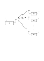
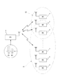
図1は、本発明を好適に適用可能な、第1実施形態に係る無線通信システムの全体構成図である。
図1に示すように、本実施形態の無線通信システムは、基地局装置(BS:Base Station)1と、この装置1のセル内で当該装置1と無線通信を行う複数の移動端末(MS:Mobile Station)2とから構成されている。
Hereinafter, embodiments of the present invention will be described with reference to the drawings.
[First Embodiment]
[Wireless communication system]
FIG. 1 is an overall configuration diagram of a radio communication system according to the first embodiment to which the present invention can be preferably applied.
As shown in FIG. 1, a wireless communication system according to the present embodiment includes a base station device (BS: Base Station) 1 and a plurality of mobile terminals (MSs) that perform wireless communication with the
この無線通信システムでは、基地局装置1と移動端末2との間の変調方式として、OFDM方式が採用されている。この方式は、送信データを多数の搬送波(サブキャリア)に乗せるマルチキャリアのデジタル変調方式であり、各サブキャリアは互いに直交しているため、周波数軸で重なりが生じる程に密にデータを並べられる利点がある。
In this radio communication system, an OFDM scheme is adopted as a modulation scheme between the
また、本実施形態の無線通信システムは、LTE(Long Term Evolution )方式が適用される携帯電話用のシステムよりなり、各基地局装置1と移動端末2との間においてLTE方式に準拠した通信が行われる。
もっとも、本発明を適用可能な無線通信システムはLTEに限られるものではなく、W−CDMAを採用してもよい。
The wireless communication system of the present embodiment is a mobile phone system to which the LTE (Long Term Evolution) system is applied, and communication based on the LTE system is performed between each
But the radio | wireless communications system which can apply this invention is not restricted to LTE, You may employ | adopt W-CDMA.
〔LTEのダウンリンクフレーム〕
図7は、LTEのダウンリンクフレームの構造を示す図である。図中、縦軸方向は周波数を示しており、横軸方向は時間を示している。
図7に示すように、ダウンリンク(DL)フレームを構成する合計10個のサブフレーム(subframe♯0〜♯9)は、それぞれ2つのスロット(slot♯0とslot♯1)により構成されており、1つのスロットは7個のOFDMシンボルにより構成されている(Normal Cyclic Prefixの場合)。
[LTE downlink frame]
FIG. 7 is a diagram illustrating a structure of an LTE downlink frame. In the figure, the vertical axis direction represents frequency, and the horizontal axis direction represents time.
As shown in FIG. 7, a total of ten subframes (
また、図中、データ伝送の上での基本単位であるリソースブロック(RB:Resource Block)は、周波数軸方向に12サブキャリア、時間軸方向に7OFDMシンボル(1スロット)として定められている。
従って、例えば、DLフレームの周波数帯域幅が5MHzに設定されている場合には、300個のサブキャリアが配列されるので、リソースブロックは、周波数軸方向に25個配置される。
Also, in the figure, a resource block (RB: Resource Block) which is a basic unit in data transmission is defined as 12 subcarriers in the frequency axis direction and 7 OFDM symbols (1 slot) in the time axis direction.
Therefore, for example, when the frequency bandwidth of the DL frame is set to 5 MHz, since 300 subcarriers are arranged, 25 resource blocks are arranged in the frequency axis direction.
なお、1つのサブフレームの送信時間は1msであり、本実施形態では、1つのサブフレームを構成する2つのスロットがそれぞれ7個のOFDMシンボルを含むので、1つのOFDMシンボルの送信周期(シンボル周期)は、1/14ms(=約0.071ms)となっている。 Note that the transmission time of one subframe is 1 ms, and in this embodiment, since two slots constituting one subframe each include seven OFDM symbols, the transmission period (symbol period) of one OFDM symbol. ) Is 1/14 ms (= about 0.071 ms).
図7に示すように、各サブフレームの先頭には、基地局装置1が移動端末2に対し、下り通信に必要な情報を送信するための制御チャネルが割り当てられている。
この制御チャネルには、DL制御情報や、当該サブフレームのリソース割当情報、ハイブリッド自動再送要求(HARQ:Hybrid Automatic Report Request)による受信成功通知(ACK:Acknowledgement)、受信失敗通知(NACK:Negative Acknowledgement)等が格納される。
As shown in FIG. 7, a control channel for transmitting information necessary for downlink communication from the
In this control channel, DL control information, resource allocation information of the subframe, reception success notification (ACK: Acknowledgement) by hybrid automatic retransmission request (HARQ: Hybrid Automatic Report Request), reception failure notification (NACK: Negative Acknowledgement) Etc. are stored.
図7に示すDLフレームにおいて、PBCH(Physical Broadcast CHannel)は、ブロードキャスト送信によってシステムの帯域幅等を端末装置に通知するための同報チャネルであり、0番目(♯0)及び6番目(♯5)のサブフレームには、基地局装置1やセルを識別するための信号である、第1同期信号(P−SCH:Primary Synchronization CHannel)及び第2同期信号(S−SCH:Secondary Synchronization CHannel)が割り当てられている。
In the DL frame shown in FIG. 7, PBCH (Physical Broadcast CHannel) is a broadcast channel for notifying the terminal device of the system bandwidth and the like by broadcast transmission, and is 0th (# 0) and 6th (# 5). ) Includes a first synchronization signal (P-SCH: Primary Synchronization CHannel) and a second synchronization signal (S-SCH: Secondary Synchronization CHannel), which are signals for identifying the
また、上記の各チャネルが割り当てられていない他の領域(図7中でハッチングのない領域)のリソースブロックは、ユーザデータ等を格納するためのDL共有通信チャネル(PDSCH:Physical Downlink Shared CHannel)として用いられる。
上記PDSCHに格納されるユーザデータの割り当てについては、各サブフレームの先頭に割り当てられている上記制御チャネル内のリソース割当情報で規定されており、移動端末2は、このリソース割当情報により、自己に対するデータがサブフレーム内に格納されているか否かを判断できる。
Also, resource blocks in other areas to which the above channels are not assigned (areas without hatching in FIG. 7) are DL shared communication channels (PDSCHs) for storing user data and the like. Used.
The allocation of user data stored in the PDSCH is defined by the resource allocation information in the control channel allocated at the head of each subframe, and the
〔送信機の構成〕
図2は、基地局装置1のOFDM送信機3の要部を示す機能ブロック図である。
この送信機3は、送信用プロセッサ4と電力増幅回路5とを備えている。送信用プロセッサ4は、例えば、1又は複数のメモリやCPUを内部に有するFPGA(Field Programmable Gate Array )により構成されている。
[Configuration of transmitter]
FIG. 2 is a functional block diagram illustrating a main part of the
The
上記FPGAは、プロセッサの出荷時や基地局装置1の製造時等において、各種の論理回路に対する構成情報を予め設定(コンフィギュレーション)可能である。かかる設定作業を経ることにより、図2に示す各機能部6〜8が構成されている。
すなわち、本実施形態の送信用プロセッサ4は、左から順に、S/P変換部6、マッピング部7、及び、IFFT(Inverse Fast Fourier Transform:逆高速フーリエ変換)部8を含んでいる。
The FPGA can set (configure) configuration information for various logic circuits in advance at the time of shipment of the processor, manufacture of the
That is, the
送信用プロセッサ4に入力されたシリアルの信号列は、S/P(シリアルパラレル)変換部6において複数の信号列に変換される。変換された各パラレルの信号列は、マッピング部7において、所定の振幅と位相の組み合わせからなる複数のサブキャリア信号f1,f2,……fnに変換される。
この各サブキャリア信号f1,f2,……fnは、IFFT部8によって時間軸上で互いに直交するベースバンド信号としてのI信号及びQ信号に変換される。このIQ信号(Iin,Qin)は、後段の電力増幅回路5に入力される。
The serial signal sequence input to the
Each of the subcarrier signals f1, f2,... Fn is converted into an I signal and a Q signal as baseband signals orthogonal to each other on the time axis by the
〔電力増幅回路の構成〕
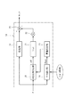
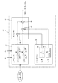
図3は、第1実施形態に係る電力増幅回路5の機能ブロック図である。
本実施形態の電力増幅回路5は、前記EER方式を採用しており、入力側のIQ信号からその振幅情報(エンベロープ)を抽出し、これをパワーアンプ16の電源電圧として印加することにより、パワーアンプ16をほぼ飽和に近い状態で動作させるものである。
[Configuration of power amplifier circuit]
FIG. 3 is a functional block diagram of the
The
図3に示すように、この電力増幅回路5は、具体的には、ポーラ変調部11、CFR処理部14、ドレイン電圧変調部15及びパワーアンプ16を備えている。
このうち、ポーラ変調部11は、直交座標形式のIQベースバンド信号から振幅成分と位相成分に分離するものであり、IQベースバンド信号の電力算出部12と位相変調部13とから構成されている。
As shown in FIG. 3, the
Among these, the
電力算出部12は、入力側のI信号とQ信号(Iin,Qin)の2乗和よりなるIQベースバンド信号の瞬時電力P(=I2+Q2)を算出するものである。算出された瞬時電力Pは後段のCFR処理部14に入力される。
位相変調部13は、IQベースバンド信号の位相成分を抽出する抽出回路と、抽出した位相成分をRF(Radio Frequency )の高周波に変調する変調器と、変調信号の振幅を一定にするリミッター等よりなり、位相変調部13が出力する位相変調信号はRFラインを通じてパワーアンプ16に入力される。
The
The
CFR処理部14は、電力算出部12から入力された瞬時電力Pが所定の閾値Pthを超えないようにその上限を制限するCFR回路よりなるが、その詳細は後述する。
ドレイン電圧変調部15は、CFR処理部14によって上限が制限されたIQベースバースト信号の瞬時電力Pを増幅する増幅器(例えばD級アンプ)と、増幅信号の最大値を保持するピークホールド回路等よりなり、瞬時電力Pに応じた振幅変調信号を出力する。
The
The drain
パワーアンプ16は、例えば、FET(Field Effect Transistor)型のトランジスタよりなる。
パワーアンプ16は、位相変調部13からの位相変調信号をゲート端子への入力信号とし、ドレイン電圧変調部15からの振幅変調信号をドレイン端子への電源電圧として常にほぼ飽和付近で動作する。これにより、パワーアンプ16が乗算器として動作し、位相変調信号と振幅変調信号が合成されて、高効率で増幅された出力変調信号が得られる。
The
The
〔CFR処理部の構成〕
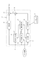
図4は、第1実施形態に係るCFR処理部(NS−CFR回路)14の機能ブロック図である。
図4に示すように、このCFR処理部14は、補正信号算出部20、フィルタ21、乗算器よりなるスケーリング部22、加減算器23、遅延部24、平均算出部25及び閾値更新部26を含む。
[Configuration of CFR processing unit]
FIG. 4 is a functional block diagram of the CFR processing unit (NS-CFR circuit) 14 according to the first embodiment.
As shown in FIG. 4, the
補正信号算出部20は、電力算出部12から入力された瞬時電力Pと、その時点で保持している閾値Pthとを比較し、瞬時電力Pが閾値Pthよりも大きい場合に、その差分ΔPを出力する。また、補正信号算出部20は、瞬時電力Pが閾値Pth以下の場合にはゼロを出力する。
補正信号算出部20が出力した差分ΔPは、それぞれ、後段のローパスフィルタやFIRフィルタ等よりなるフィルタ21により帯域制限(ノイズシェーピング)され、更にその後段のスケーリング部22によって振幅調整されて加減算器23に入力される。
The correction
The difference ΔP output from the correction
遅延部24は、補正信号算出部20その他の演算部における演算処理の時間だけ、瞬時電力Pの信号出力タイミングを遅延させる。
そして、加減算器23は、遅延された瞬時電力Pから帯域制限された補正信号ΔPを減算することにより、瞬時電力の出力信号Poutを出力する。この減算により、閾値Pthを超える瞬時電力Pについては、閾値Pth相当の瞬時電力Pに補正される。また、閾値Pth以下の瞬時電力Pについては、補正されずにそのまま出力される。
The
Then, the adder /
図5は、上記の信号処理を行った場合のIQベースバンド信号と閾値Pthとの関係を示すIQ平面の座標図である。
この図5に示すように、本実施形態のCFR処理部14による信号処理は、IQベースバンド信号の瞬時電力Pの外周側をカットするクリッピング処理である。このため、電力増幅回路5のパワーアンプ16に印加するドレイン電圧のPAPRが低下するので、パワーアンプ16の電力効率を向上させることができる。
FIG. 5 is a coordinate diagram on the IQ plane showing the relationship between the IQ baseband signal and the threshold value Pth when the above signal processing is performed.
As shown in FIG. 5, the signal processing by the
〔電力増幅回路の効果〕
本実施形態の電力増幅回路5によれば、CFR処理部14が、IQベースバンド信号の振幅成分に対応するスカラー量である瞬時電力P(=I2+Q2)の上限を所定の閾値Pth相当に制限し、パワーアンプ16が、位相変調部13からの位相変調信号を入力信号とし、上限が制限された瞬時電力Pに応じた振幅変調信号を電源電圧として動作する。
従って、IQベースバンド信号に大きなピーク変動があっても、それに伴ってパワーアンプ16の電源電圧が大きく変動することがなく、パワーアンプ16の電力効率を効果的に高めることができる。
[Effect of power amplifier circuit]
According to the
Therefore, even if there is a large peak fluctuation in the IQ baseband signal, the power supply voltage of the
また、本実施形態の電力増幅回路5によれば、図3に示すように、電力算出部12とドレイン電圧変調部15の間にCFR処理部14を配置し、IQベースバンド信号の瞬時電力Pの上限を所定の閾値Pth相当に制限した上で、制限後の瞬時電力Pout をドレイン電圧変調部15に供給する回路配置となっている。
このため、図4に示すように、瞬時電力Pに逆向きの相殺信号を与えるための回路構成として、フィルタ21、乗算器22、加減算器23及び遅延回路24を1つだけ実装すれば足りる。
Further, according to the
Therefore, as shown in FIG. 4, it is sufficient to mount only one
従って、IQベースバンド信号のI成分とQ成分のそれぞれに減算を行ってピーク電力を制限するCFR回路と比べて、上記の構成要素が少なくて済み、回路規模の小さいCFR回路を採用することができ、パワーアンプ16を効果的に高効率化できる電力増幅回路5を安価に実現することができる。
Therefore, compared to a CFR circuit that limits the peak power by subtracting each of the I component and Q component of the IQ baseband signal, it is possible to use a CFR circuit that requires fewer components and has a smaller circuit scale. Thus, the
〔閾値更新部について〕
図4に戻り、平均算出部25は、送信電力が大きく変動し得る最小の時間単位であるOFDMシンボルのシンボル周期を、平均電力を算出する制御周期として取得している。
また、平均算出部25は、電力算出部12からIQベースバンド信号の瞬時電力Pを取得しており、その瞬時電力Pを上記シンボル周期内で平均化することにより、シンボル周期ごとのIQベースバンド信号の平均電力Pave を算出し、これを閾値更新部26に出力する。
[About the threshold update unit]
Returning to FIG. 4, the
The
閾値更新部26は、平均算出部25から取得したシンボル周期ごとの平均電力Pave に所定の倍率を乗算した値を、そのシンボル周期における閾値Pthとして採用する。例えば、IQベースバンド信号のピーク電力Ppeakと平均電力Pave との比率を6dBに絞る場合には、上記所定の倍率は2倍となる。
閾値更新部26は、上記のようにしてシンボル周期ごとに閾値Pthを算出して当該閾値Pthを動的に更新し、その更新した閾値Pthを補正信号算出部20に出力する。
The
The
そして、補正信号算出部20は、閾値更新部26から取得した閾値Pthを用いて、電力算出部12が算出した瞬時電力Pの大小を判定し、瞬時電力Pが更新後の閾値Pthを超えているか否かを判定する。
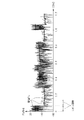
図6は、IQベースバンド信号の瞬時電力Pと逐次更新される閾値Pthの時間的変化の一例を示すグラフである。
Then, the correction
FIG. 6 is a graph showing an example of temporal changes in the instantaneous power P of the IQ baseband signal and the threshold value Pth that is sequentially updated.
図6に示すように、本実施形態では、CFR処理部14で用いる閾値Pthが、シンボル周期(1/14ms)ごとに算出した平均電力Pave に基づいて逐次算出され、そのシンボル周期ごとに更新される。
このため、例えば、移動端末2による通話量の変動に対応して、IQベースバンド信号の平均電力Pave が変動してもクリッピング処理が適切に行われることになるので、PAPRの低減によるパワーアンプ16の電力効率の向上を、有効に確保することができる。
As shown in FIG. 6, in the present embodiment, the threshold value Pth used in the
For this reason, for example, the clipping process is appropriately performed even if the average power Pave of the IQ baseband signal fluctuates in response to fluctuations in the call volume by the
また、本実施形態によれば、閾値Pthを更新する制御周期として、送信電力が変動し得る最小の時間単位であるOFDMのシンボル周期を採用しているので、閾値Pthを正確かつ迅速に更新できるという利点もある。
もっとも、LTEでは、リソースブロック(図7参照)がユーザ割当の最小単位になっているので、このリソースブロックの送信周期である7OFDMシンボル(1スロット)を、閾値Pthを更新する制御周期として採用することにしてもよい。
Further, according to the present embodiment, since the OFDM symbol period, which is the minimum time unit in which the transmission power can be varied, is employed as the control period for updating the threshold value Pth, the threshold value Pth can be updated accurately and quickly. There is also an advantage.
However, in LTE, the resource block (see FIG. 7) is the minimum unit for user allocation, and therefore 7 OFDM symbols (1 slot), which is the transmission period of this resource block, is adopted as the control period for updating the threshold value Pth. You may decide.
〔無線通信システムの変形例〕
図8は、無線通信システムの変形例を示す全体構成図である。
図8に示すように、この変形例の無線通信システムでは、基地局装置1に、CPRI(Common Public Radio Interface)を介してRRH27が接続されている。基地局装置1は、RRH27との間で同期を確立するための同期信号28を、光ファイバを通じてRRH27に送出している。この同期信号28は、OFDMのシンボル周期と同期する1ms周期のクロック信号よりなる。
[Modification of wireless communication system]
FIG. 8 is an overall configuration diagram showing a modification of the radio communication system.
As shown in FIG. 8, in the radio communication system of this modification, an
第1実施形態や後述の各実施形態の電力増幅回路5を有する送信機3は、上記RRH27に搭載することにしてもよい。
この場合、外部装置である基地局装置1から取得した同期信号28からシンボル周期を生成し、生成したシンボル周期を平均算出部25(図4参照)に出力することにより、シンボル周期ごとに閾値Pthを更新可能なCFR処理部14が得られる。
The
In this case, a symbol period is generated from the
〔第2実施形態〕
第1実施形態では、電力増幅回路5のCFR処理部14がNS−CFR回路で構成されていたが、CFR処理部14をPC−CFR回路で構成することにしてもよい。
図9は、第2実施形態に係るCFR処理部(PC−CFR回路)14の機能ブロック図である。図9に示すように、このCFR処理部14は、補正信号算出部30、比較部31、パルス保持部32、乗算器33、加減算器34、遅延部35、平均算出部36及び閾値更新部37を含む。
[Second Embodiment]
In the first embodiment, the
FIG. 9 is a functional block diagram of the CFR processing unit (PC-CFR circuit) 14 according to the second embodiment. As shown in FIG. 9, the
補正信号算出部30は、電力算出部12から入力された瞬時電力Pと、その時点で保持している閾値Pthとを比較し、瞬時電力Pが閾値Pthよりも大きい場合に、その差分ΔPを乗算器33に出力する。
比較部31は、電力算出部12で算出された瞬時電力Pと閾値Pthとを比較し、瞬時電力Pが閾値Pthよりも大きい場合に、相殺用パルスSの出力指令をパルス保持部32に発する。
The correction
The
パルス保持部32は、後述の合成パルスよりなる相殺用パルスS(図10参照)を一時的に保持する、デュアルポートRAM等よりなるメモリを有しており、比較部31から指令を受けた場合、保持している相殺用パルスSを乗算器33に出力する。
また、パルス保持部32は、比較部31から指令を受けてない場合は、乗算器33にゼロを出力する。従って、閾値Pthを超えている瞬時電力Pについては、Pc=ΔP×Sとして算出される相殺信号Pcが加減算器34に入力される。
The
Further, the
遅延部35は、補正信号算出部30その他の演算部における演算処理の時間だけ、瞬時電力Pの信号時間を遅延させる。
そして、加減算器34は、遅延された瞬時電力Pから相殺信号Pcを減算することにより、瞬時電力の出力信号Poutを出力する。この減算により、閾値Pthを超える瞬時電力Pについては、閾値Pth相当の瞬時電力Pに補正される。また、閾値Pth以下の瞬時電力Pについては、補正されずにそのまま出力される。
The
The adder /
なお、図9に示すように、第2実施形態のCFR処理部14にも、平均算出部36と閾値更新部37が設けられているが、これらは、第1実施形態(図4)のCFR処理部14に設けられた平均算出部25及び閾値更新部26と同様の処理を行う機能部である。
As shown in FIG. 9, the
〔相殺用パルスについて〕
図10は、相殺用パルスSの生成方法を示す波形図である。
図10に示すように、本実施形態の相殺用パルスSは、基本パルスSaと補助パルスSbとを合成した合成パルスよりなる。
なお、図10においては、基本パルスSaの時間波形と周波数スペクトルが左上枠内に示され、補助パルスSbの時間波形と周波数スペクトルが左下枠内に示されている。また、相殺用パルスSの時間波形と周波数スペクトルが右枠内に示されている。
[About canceling pulse]
FIG. 10 is a waveform diagram showing a generation method of the cancellation pulse S.
As shown in FIG. 10, the cancellation pulse S of the present embodiment is composed of a synthesized pulse obtained by synthesizing a basic pulse Sa and an auxiliary pulse Sb.
In FIG. 10, the time waveform and frequency spectrum of the basic pulse Sa are shown in the upper left frame, and the time waveform and frequency spectrum of the auxiliary pulse Sb are shown in the lower left frame. The time waveform and frequency spectrum of the canceling pulse S are shown in the right frame.
上記基本パルスSaは、特許文献3(特開2004−135078号公報)の場合と同様に、下り信号の送信に使用する帯域(以下、「使用帯域」ということがある。)Bに含まれる複数本(例えば、N本とする。)の搬送波を、振幅を1/Nにしかつ位相を0にして、前記IFFT部8に入力して得られたSinc波形よりなるものである。この場合、IFFT部8の出力には実部Iだけが出現し、虚部Qはゼロになる。
As in the case of Patent Document 3 (Japanese Patent Laid-Open No. 2004-135078), the basic pulse Sa is a plurality of bands included in a band (hereinafter sometimes referred to as “used band”) B used for transmission of a downlink signal. This is a sinc waveform obtained by inputting the number of carrier waves (for example, N) into the
このように、基本パルスSaは、IQベースバンド信号の周波数帯域Bに含まれる複数本のサブキャリアに対して、その信号の場合と同じIFFT部8で逆フーリエ変換を行って得られた実部Iの波形(Sinc波形)である。
従って、基本パルスSaの周波数帯域は使用帯域Bと一致しており、閾値Pthを超える瞬時電力Pの増分ΔPに基本パルスaを乗算した相殺信号を用いて瞬時電力Pをクリッピングしても、使用帯域Bの外部に不要な周波数成分は発生しない。
Thus, the basic pulse Sa is obtained by performing inverse Fourier transform on the plurality of subcarriers included in the frequency band B of the IQ baseband signal by the
Accordingly, the frequency band of the basic pulse Sa matches the use band B, and even if the instantaneous power P is clipped using the cancellation signal obtained by multiplying the increment ΔP of the instantaneous power P exceeding the threshold Pth by the basic pulse a, it is used. No unnecessary frequency component is generated outside the band B.
しかし、上記基本パルスSaでは、送信に使用する周波数帯域B内の信号成分のみを用いているので、図10の左上枠内の時間波形に示すように、その時間軸上のパルス幅を余り細くすることができない。
このため、上記基本パルスSaのみを相殺用パルスSとして採用し、それを増分ΔPに乗算して求めた相殺信号Pcで瞬時電力Pを相殺すると、相殺信号Pcがピーク時以降の電力波形と干渉して新たなピーク波形が生成され、ピーク電力を確実に抑制できない場合がある。
However, since only the signal component within the frequency band B used for transmission is used in the basic pulse Sa, the pulse width on the time axis is made too narrow as shown in the time waveform in the upper left frame of FIG. Can not do it.
For this reason, when only the basic pulse Sa is adopted as the cancellation pulse S and the instantaneous power P is canceled by the cancellation signal Pc obtained by multiplying it by the increment ΔP, the cancellation signal Pc interferes with the power waveform after the peak time. As a result, a new peak waveform is generated, and the peak power may not be reliably suppressed.
そこで、本実施形態では、使用帯域B外の帯域でも、ある程度のピーク電力の抑制を適切に行えるようにするため、基本パルスSaの他に補助パルスSbを定義し、この補助パルスSbを基本パルスSaに合成したものを相殺用パルスSとして採用している。
この補助パルスSbは、図10の左下枠内の時間波形に示すように、基本パルスSaのピークが立つ時間において急峻に立ち上がり、基本パルスSaよりも細幅の非常に細いデルタ関数に近いパルス波形よりなる。
Therefore, in this embodiment, in order to appropriately suppress a certain amount of peak power even in a band outside the use band B, an auxiliary pulse Sb is defined in addition to the basic pulse Sa, and the auxiliary pulse Sb is used as the basic pulse. A composition combined with Sa is used as the canceling pulse S.
As shown in the time waveform in the lower left frame of FIG. 10, the auxiliary pulse Sb rises sharply at the time when the peak of the basic pulse Sa rises, and has a pulse waveform close to a delta function that is narrower than the basic pulse Sa. It becomes more.
従って、補助パルスSbの周波数スペクトルは、使用帯域Bを含む非常に広い帯域(以下、「広範帯域」ということがある。)Bwになっている。
このように、本実施形態の相殺用パルスSは、従来の基本パルスSaに上記補助パルスSbを合成した合成パルスよりなるので、図10の右枠内の周波数スペクトルに示すように、IQベースバンド信号の周波数帯域Bだけでなく、その帯域Bから外れた広範帯域Bwの周波数成分を有している。
Therefore, the frequency spectrum of the auxiliary pulse Sb is a very wide band including the use band B (hereinafter, also referred to as “broad band”) Bw.
Thus, the cancellation pulse S of the present embodiment is composed of a synthesized pulse obtained by synthesizing the auxiliary pulse Sb with the conventional basic pulse Sa. Therefore, as shown in the frequency spectrum in the right frame of FIG. It has not only the frequency band B of the signal but also a frequency component of a wide band Bw outside the band B.
〔各パルスのピークレベル〕
また、本実施形態では、基本パルスSaのピークレベルをαとし、補助パルスSbのピークレベルをβとすると、0.03≦β/α≦0.1を満足するように、それらのレベルα,βの比率を設定している。以下、その理由について説明する。
[Peak level of each pulse]
Further, in the present embodiment, when the peak level of the basic pulse Sa is α and the peak level of the auxiliary pulse Sb is β, those levels α and so that 0.03 ≦ β / α ≦ 0.1 are satisfied. The ratio of β is set. The reason will be described below.
上記の通り、補助パルスSbの周波数成分は、IQベースバンド信号の使用帯域Bから外れた広範帯域Bwに渡っているので、補助パルスSbを含む合成パルスを用いて求めた相殺信号Pcを瞬時電力Pから減算すると、広い周波数帯域Bwに渡ってノイズが印加されるのと同じ結果となる。
このため、基本パルスSaと補助パルスSbのレベルを適切に設定しないと、使用帯域Bにおける通信品質(EVM)が悪化したり、使用帯域Bの帯域外に高レベルのノイズが発生したりする可能性がある。
As described above, since the frequency component of the auxiliary pulse Sb extends over a wide band Bw that deviates from the use band B of the IQ baseband signal, the cancellation signal Pc obtained using the synthesized pulse including the auxiliary pulse Sb is used as the instantaneous power. Subtracting from P gives the same result as applying noise over a wide frequency band Bw.
For this reason, if the levels of the basic pulse Sa and the auxiliary pulse Sb are not set appropriately, the communication quality (EVM) in the use band B may be deteriorated, or high-level noise may be generated outside the use band B. There is sex.
ここで、例えばLTEにおいて、使用帯域BにおけるEVMが40dBを確保することが要請され、また、近隣チャネル漏洩電力比については、電波法上で60dBを確保することが要請されているとする。
従って、補助パルスSbの合成によって使用帯域Bに許容される電力低下は、最大で20dBであり、これを電圧に換算すると0.1となる。よって、補助パルスSbのピークレベル(電圧)の比率β/αは、最大で0.1まで許容可能である。
Here, for example, in LTE, it is assumed that the EVM in the use band B is required to secure 40 dB, and the adjacent channel leakage power ratio is required to be secured 60 dB according to the Radio Law.
Therefore, the power reduction allowed in the use band B by the synthesis of the auxiliary pulse Sb is 20 dB at the maximum, and becomes 0.1 when converted into a voltage. Therefore, the peak level (voltage) ratio β / α of the auxiliary pulse Sb is allowable up to 0.1.
一方、補助パルスSbのピークレベルが小さ過ぎると、相殺信号Pcの減算によって生じる新たなピーク波形を適切にキャンセルできない恐れがあるが、補助パルスSbのピークレベル(電圧)の比率β/αは、最小で0.03程度あれば、新たなピーク波形をキャンセルできることが判明している。
以上から、各パルスS1,S2のピークレベルα,βについては、0.03≦β/α≦0.1を満足するように、それらのレベルα,βの比率を設定すればよいということになる。
On the other hand, if the peak level of the auxiliary pulse Sb is too small, there is a possibility that a new peak waveform generated by subtraction of the cancellation signal Pc cannot be canceled appropriately. However, the ratio β / α of the peak level (voltage) of the auxiliary pulse Sb is It has been found that a new peak waveform can be canceled with a minimum of about 0.03.
From the above, regarding the peak levels α and β of the pulses S1 and S2, the ratio of the levels α and β may be set so as to satisfy 0.03 ≦ β / α ≦ 0.1. Become.
本実施形態のCFR処理部14によれば、IQベースバンド信号の周波数帯域B内の周波数成分だけでなく、その帯域外の周波数成分をも有する相殺用パルスS(図10参照)を閾値Pthからの増分ΔPに乗算して得られた相殺信号Pcを、瞬時電力Pに減算する。
このため、帯域外の周波数成分に影響する相殺信号Pcの減算により、新たなピーク波形が生じるのを防止でき、IQベースバンド信号のピーク電力をより確実に抑制することができる。
According to the
For this reason, it is possible to prevent a new peak waveform from being generated by subtraction of the cancellation signal Pc that affects the frequency component outside the band, and it is possible to more reliably suppress the peak power of the IQ baseband signal.
〔第3実施形態〕
図11は、第3実施形態に係る無線通信システムの全体構成図である。また、図12は、その場合の基地局装置1のOFDM送信機3の要部を示す機能ブロック図である。
本実施形態においても、LTE方式に基づく無線通信システムが採用されている。この方式の基地局装置1では、例えば5MHz単位でダウンリンクフレームの周波数帯域を設定可能であり、セル内の各移動端末2に下り信号を送信する場合において、その周波数帯域ごとに送信電力を変更可能になっている。
[Third Embodiment]
FIG. 11 is an overall configuration diagram of a wireless communication system according to the third embodiment. FIG. 12 is a functional block diagram showing a main part of the
Also in this embodiment, a radio communication system based on the LTE scheme is employed. In this type of
本実施形態の基地局装置1では、2種類の周波数帯域B1,B2でダウンリンクフレームを送信する場合を例示しており、周波数が小さい方の第1帯域B1の送信電力が大きく設定され、周波数が大きい方の第2帯域B2での送信電力が小さく設定されている。
このため、図11に破線で示すように、送信電力が大きい第1帯域B1の下り信号が届く通信エリアA1は、送信電力が小さい第2帯域B2の下り信号が届く通信エリアA2よりも遠方でかつ広範囲になっている。
The
For this reason, as shown by a broken line in FIG. 11, the communication area A1 in which the downlink signal of the first band B1 with high transmission power reaches is farther than the communication area A2 in which the downlink signal of the second band B2 with low transmission power reaches. And it has become widespread.
上記通信エリアA1,A2が重複するエリア内では、移動端末2が第1及び第2帯域B1,B2が双方で通信可能となるので、通話量が多い場合でも移動端末2の通信が確実に行われることになる。
In the area where the communication areas A1 and A2 overlap, the
本実施形態では、基地局装置1が2種類の周波数帯域B1,B2で下り信号を送信する場合を想定しているので、図12に示すように、サブキャリアが第1帯域B1に含まれる第1信号I1,Q1と、サブキャリアが第2帯域B2に含まれる第2信号I2,Q2とがIFFT部8から出力される。
この第1信号I1,Q1と第2信号I2,Q2は、後段の電力増幅回路5に入力され、この回路5において所定の信号処理が施される。
In this embodiment, since it is assumed that the
The first signals I1 and Q1 and the second signals I2 and Q2 are input to the
〔CFR処理部の構成〕
図13は、第3実施形態に係るCFR処理部(PC−CFR回路)14の機能ブロック図である。図13に示すように、本実施形態のCFR処理部14(図13)が第2実施形態のCFR処理部(図9)と異なる点は、周波数帯域ごとの平均電力に対応して瞬時電力Pを相殺可能な相殺用パルスSを生成する、パルス生成部40を備えている点にある。
[Configuration of CFR processing unit]
FIG. 13 is a functional block diagram of the CFR processing unit (PC-CFR circuit) 14 according to the third embodiment. As shown in FIG. 13, the CFR processing unit 14 (FIG. 13) of the present embodiment differs from the CFR processing unit (FIG. 9) of the second embodiment in that the instantaneous power P corresponds to the average power for each frequency band. Is provided with a
以下、第2実施形態と共通する構成及び機能は図面に同一符号を付して説明を省略し、第2実施形態との相違点について重点的に説明する。
なお、以下において、第1信号I1,Q1と第2信号I2,Q2の合成信号を単に「IQベースバンド信号」或いは「IQ信号」というものとする。
また、第1信号I1,Q1の瞬時電力をP1とし、第2信号I2,Q2の瞬時電力をP2とし、IQベースバンド信号の瞬時電力をP(=P1+P2)とする。
Hereinafter, configurations and functions common to the second embodiment will be denoted by the same reference numerals in the drawings, description thereof will be omitted, and differences from the second embodiment will be mainly described.
In the following, the combined signal of the first signal I1, Q1 and the second signal I2, Q2 is simply referred to as “IQ baseband signal” or “IQ signal”.
The instantaneous power of the first signals I1 and Q1 is P1, the instantaneous power of the second signals I2 and Q2 is P2, and the instantaneous power of the IQ baseband signal is P (= P1 + P2).
本実施形態のCFR処理部14の前段には、瞬時電力Pを算出する電力算出部12の他に、第1算出部41と第2算出部42が設けられている。
このうち、第1算出部41は、第1信号I1,Q1のI成分とQ成分の2乗和よりなる第1信号I1,Q1の瞬時電力P1(=I12+Q12)を算出する。第2算出部42は、第2信号I2,Q2のI成分とQ成分の2乗和よりなる第2信号I2,Q2の瞬時電力P2(=I22+Q22)を算出する。
A
Of these, the first calculating
〔パルス生成部の構成〕
図14は、パルス生成部40の機能ブロック図である。
このパルス生成部40は、第1及び第2帯域B1,B2ごとに予め求められた合成パルスS1,S2に、その帯域B1,B2ごとの平均電力の相対比率C1,C2をそれぞれ乗算して総和をとることにより、前記相殺用パルスSを生成するものであり、比率算出部43、波形記憶部44及び乗加算部45を有している。
[Configuration of pulse generator]
FIG. 14 is a functional block diagram of the
The
このうち、波形記憶部44は、周波数帯域B1,B2ごとの合成パルスS1,S2を記憶するメモリ等の記憶装置よりなる。この合成パルスS1,S2は、第2実施形態の場合と同様に、基本パルスSaと補助パルスSb(図4)とを合成したものである。
すなわち、第1帯域B1用の合成パルスS1は、第1帯域B1に含まれる複数本のサブキャリアに対して、送信信号の場合と同じIFFT部8で逆フーリエ変換を行って得られた実部Iの波形よりなる基本パルスSaに、補助パルスSbを合成したものである。
Among these, the waveform memory |
That is, the composite pulse S1 for the first band B1 is a real part obtained by performing inverse Fourier transform on the plurality of subcarriers included in the first band B1 by the
また、第2帯域B2用の合成パルスS2は、第2帯域B2に含まれる複数本のサブキャリアに対して、送信信号の場合と同じIFFT部8で逆フーリエ変換を行って得られた実部Iの波形よりなる基本パルスSaに、補助パルスSbを合成したものである。
もっとも、本実施形態において、補助パルスSbを考慮せずに、基本パルスSaのみから各周波数帯域B1,B2のパルスS1,S2を構成することにしてもよい。
The synthesized pulse S2 for the second band B2 is a real part obtained by performing inverse Fourier transform on the plurality of subcarriers included in the second band B2 by the
However, in the present embodiment, the pulses S1 and S2 of the frequency bands B1 and B2 may be configured only from the basic pulse Sa without considering the auxiliary pulse Sb.
比率算出部43には、第1算出部41が算出する第1信号I1,Q1の瞬時電力P1と、第2算出部42が算出する第2信号I2,Q2の瞬時電力P2がそれぞれ入力される。
比率算出部43は、これらの瞬時電力P1,P2を用いて、周波数帯域B1,B2ごとの平均電力の相対比率C1,C2を、次式に基づいて算出する。
C1=Σ√P1/(Σ√P1+Σ√P2)
C2=Σ√P2/(Σ√P1+Σ√P2)
The
The
C1 = Σ√P1 / (Σ√P1 + Σ√P2)
C2 = Σ√P2 / (Σ√P1 + Σ√P2)
上記算出式に示すように、周波数帯域B1,B2ごとの平均電力の相対比率C1,C2は、その周波数帯域B1,B2ごとの瞬時電力P1,P2の平方根√P1,√P2を所定のサンプリング周期で累積し、その累積値Σ√P1,Σ√P2を、各周波数帯域B1,B2の累積値の総和(Σ√P1+Σ√P2)で除算することによって求められる。 As shown in the above calculation formula, the relative ratios C1 and C2 of the average power for each of the frequency bands B1 and B2 are the square roots √P1 and √P2 of the instantaneous powers P1 and P2 for each of the frequency bands B1 and B2, and a predetermined sampling period. And the accumulated values Σ√P1, Σ√P2 are divided by the sum of the accumulated values of each frequency band B1, B2 (Σ√P1 + Σ√P2).
比率算出部43は、送信電力が大きく変動し得る最小の時間単位であるOFDMシンボルのシンボル周期を制御周期として取得しており、このシンボル周期内において上記相対比率C1,C2の算出を実行するようになっている。
このようにすれば、IQベースバンド信号の平均電力が余り変動しない安定状態で相対比率C1,C2を算出できるので、正確な相対比率C1,C2が得られるという効果がある。
The
In this way, since the relative ratios C1 and C2 can be calculated in a stable state where the average power of the IQ baseband signal does not change much, there is an effect that accurate relative ratios C1 and C2 can be obtained.
もっとも、 LTEでは、リソースブロック(図7参照)がユーザ割当の最小単位になっているので、このリソースブロックの送信周期である7OFDMシンボル(1スロット)を、相対比率C1,C2を算出する際の制御周期として採用することにしてもよい。 However, in LTE, the resource block (see FIG. 7) is the minimum unit for user allocation, and therefore 7 OFDM symbols (1 slot), which is the transmission period of this resource block, are used to calculate the relative ratios C1 and C2. You may decide to employ | adopt as a control period.
乗加算部45は、2つの乗算器46,47と1つの加算器48とを含む。このうち、乗算器46は、第1帯域B1に対応する相対比率C1にその帯域B1用のパルスS1を乗算し、乗算器47は、第2帯域B2に対応する相対比率C2にその帯域B2用のパルスC2を乗算する。
また、加算器48は、各乗算器46,47の乗算結果を加算して相殺用パルスSを生成し、このパルスSをCFR処理部14のパルス保持部32に出力する。すなわち、乗加算部45は、次の式に基づいて相殺用パルスSを生成する。
S=C1×S1+C2×S2
Multiplier /
The
S = C1 * S1 + C2 * S2
本実施形態の乗加算部45は、比率算出部43で算出された相対比率C1,C2を所定の閾値と比較してその変動を判定しており、相対比率C1,C2が閾値を超える程度に変動した場合にのみ、その変動後の相対比率C1,C2を用いた乗算及び総和を実行し、その結果生成された相殺用パルスSをパルス保持部32に出力する。
このため、相対比率C1,C2がある程度変動しない限り、乗加算部45が乗算及び総和を実行せず、パルス保持部32が従前の相殺用パルスSを維持する。従って、相殺用パルスSを愚直に毎回生成する場合に比べて、回路の演算負荷を低減することができる。
The multiplication /
Therefore, unless the relative ratios C1 and C2 change to some extent, the multiplication /
上記相殺用パルスSは、第1帯域B1に対応する第1信号I1,Q1の平均電力の相対比率C1に、その帯域B1用の合成パルスS1を乗算したものと、第2帯域B2に対応する第2信号I2,Q2の平均電力の相対比率C2に、その帯域B2用の合成パルスS2を乗算したものとを、加算したものになっている。
このため、上記相殺用パルスSを増分ΔPに乗算した相殺信号Pcを元の瞬時電力Pから減算しても、第1及び第2帯域B1,B2ごとの平均電力に対応して瞬時電力Pの振幅が相殺されることになる。
The cancellation pulse S corresponds to the second band B2 obtained by multiplying the relative ratio C1 of the average power of the first signals I1 and Q1 corresponding to the first band B1 by the combined pulse S1 for the band B1. This is the sum of the relative ratio C2 of the average power of the second signals I2 and Q2 multiplied by the composite pulse S2 for the band B2.
Therefore, even if the cancellation signal Pc obtained by multiplying the cancellation pulse S by the increment ΔP is subtracted from the original instantaneous power P, the instantaneous power P of the first and second bands B1 and B2 corresponds to the average power. The amplitude will be canceled out.
従って、本実施形態のCFR処理部14によれば、第1及び第2帯域B1,B2における平均電力に差がある場合でも、平均電力が小さい方の帯域B2の送信電力が、相殺信号Pcの減算によって必要以上に低下することがなく、周波数帯域B1,B2ごとに平均電力が異なるIQベースバンド信号の瞬時電力Pの場合でも、SNRを悪化させずに適切にクリッピング処理することができる。
Therefore, according to the
〔基本パルスのバリエーション〕
図15は、基本バルスSaのバリエーションを示す時間領域のグラフである。図15において、(a)はSinc波形、(b)はチェビシェフ波形、(c)はテーラー波形である。
これらの波形は、数学的には、すべて次の式(1)で表すことができ、Sinc波形の場合にはan=nπとなっている。
[Basic pulse variations]
FIG. 15 is a time-domain graph showing variations of the basic pulse Sa. In FIG. 15, (a) is a Sinc waveform, (b) is a Chebyshev waveform, and (c) is a Taylor waveform.
These waveforms can be expressed mathematically by the following equation (1), and in the case of a Sinc waveform, an = nπ.

ここで、絶対値の最大値を含み振幅値がゼロになるまでの区間(図15のハッチングで示す区間)をメインローブ区間ということにすると、Sinc波形の場合には、サイドローブの振幅が比較的大きくなるため、メインローブ区間のエネルギー局在率を余り向上させることができない。
これに対して、チェビシェフ波形では、振幅値=0となるxの解を構成する数列anの値を調整することで、サイドローブの振幅を小さくできるが、この場合には振幅が減衰しなくなる。
Here, if the section including the maximum absolute value and the amplitude value becomes zero (section indicated by hatching in FIG. 15) is referred to as a main lobe section, the side lobe amplitude is compared in the case of the Sinc waveform. Therefore, the energy localization rate in the main lobe section cannot be improved much.
On the other hand, in the Chebyshev waveform, the amplitude of the side lobe can be reduced by adjusting the value of the numerical sequence an constituting the solution of x where the amplitude value = 0, but in this case, the amplitude is not attenuated.
そこで、テーラー波形では、数列anの始めの数点(例えばa1とa2)の値をチェビシェフ波形のものを使用し、それ以降の点の値をSinc波形のものを使用しており、これにより、サイドローブの振幅抑制と減衰特性の双方を達成している。
従って、基本パルスSaを定義する所定の時間区間Tにおける全エネルギー(振幅の2乗)に対する、メインローブ区間のエネルギー局在率を比較すると、Sinc波形の場合には91%であり、チェビシェフ波形の場合には93%であり、テーラー波形の場合には約95%になり、テーラー波形が最も有利となる。
Therefore, the tailor waveform uses Chebyshev waveform values for the first few points (for example, a1 and a2) of the sequence an, and Sinc waveform values for the subsequent points. Both sidelobe amplitude suppression and attenuation characteristics are achieved.
Therefore, when the energy localization rate in the main lobe section is compared with the total energy (the square of the amplitude) in the predetermined time section T defining the basic pulse Sa, it is 91% in the case of the Sinc waveform, and the Chebyshev waveform 93% in the case, and about 95% in the case of the tailor waveform, and the tailor waveform is the most advantageous.
なお、上記所定の時間区間Tは、メモリ上に記録されている波形のサンプル時間であって、上限数のサンプル点に対応する時間である。例えば、LTEの場合には、1シンボル周期(1/14ms)に含まれるサンプル数は2048であるから、仮に時間領域で4倍のオーバーサンプリングを行うと仮定すると、基本パルスSaの波形を定義するのに必要なサンプル点の上限数は、2048×4=8192個になる。 The predetermined time interval T is a sample time of the waveform recorded on the memory and is a time corresponding to the upper limit number of sample points. For example, in the case of LTE, the number of samples included in one symbol period (1/14 ms) is 2048. Therefore, assuming that oversampling is performed four times in the time domain, the waveform of the basic pulse Sa is defined. The upper limit number of sample points necessary for this is 2048 × 4 = 8192.
PC−CFR回路に使用可能な基本パルスSaを、メインローブ区間の所定の時間区間Tに対するエネルギー局在率の数値範囲で特定すると、当該エネルギー局在率は85%〜99%であることが好ましい。
その理由は、エネルギー局在率が100%になると、基本パルスSaがインパルス(デルタ関数)となって、帯域制限がある本発明に適用できなくなり、局在率が85%未満の場合は、パルス形状が鈍化し過ぎて使用できなくなるからである。
When the basic pulse Sa that can be used in the PC-CFR circuit is specified in the numerical range of the energy localization rate with respect to the predetermined time interval T of the main lobe interval, the energy localization rate is preferably 85% to 99%. .
The reason is that when the energy localization rate becomes 100%, the basic pulse Sa becomes an impulse (delta function) and cannot be applied to the present invention with band limitation. When the localization rate is less than 85%, the pulse This is because the shape is too slow to be used.
以上から、PC−CFR回路に使用可能な基本パルスSaの技術的特徴を列挙すると、次のようになる。
特徴1:基本パルスSaは、所定の時間区間T(例えば、1シンボル周期)における全エネルギー(振幅の2乗)に対するメインローブ区間のエネルギー局在率が、85%〜99%の波形により構成できる。
From the above, the technical features of the basic pulse Sa that can be used in the PC-CFR circuit are listed as follows.
Feature 1: The basic pulse Sa can be configured by a waveform having an energy localization rate of 85% to 99% in the main lobe period with respect to the total energy (amplitude squared) in a predetermined time period T (for example, one symbol period). .
特徴2:基本パルスSaを数学的に記述すると、時間領域において対称性を持つ前記式(1)で表される波形よりなる。
特徴3:より具体的には、基本パルスSaは、Sinc波形、チェビシェフ波形又はテーラー波形よりなる。このうち、Sinc波形は、帯域内の複数本の搬送波を、振幅が同一でかつ位相をゼロにして逆フーリエ変換して得られる実部(I信号)の波形よりなる。
Characteristic 2: When the basic pulse Sa is mathematically described, it consists of a waveform represented by the formula (1) having symmetry in the time domain.
Feature 3: More specifically, the basic pulse Sa is composed of a Sinc waveform, a Chebyshev waveform, or a Taylor waveform. Among these, the Sinc waveform is a waveform of a real part (I signal) obtained by inverse Fourier transform of a plurality of carriers in the band with the same amplitude and zero phase.
〔その他の変形例〕
今回開示した実施形態は例示であって制限的なものではない。本発明の権利範囲は特許請求の範囲によって示され、特許請求の範囲の構成と均等の範囲内での全ての変更が含まれる。
例えば、本発明の電力増幅回路5は、LTE方式だけでなく、W−CDMA方式に準拠した通信装置にも採用することができる。
[Other variations]
The embodiment disclosed this time is illustrative and not restrictive. The scope of the present invention is defined by the terms of the claims, and includes all modifications that are within the scope of the claims and equivalents.
For example, the
このW−CDMA方式では、クローズドループ送信電力制御によって基地局装置1の送信電力を制御するようになっており、この制御周期が送信制御の最小時間単位となっている。具体的には、この制御周期は、1無線フレーム周期10msの15分の1(=約0.667ms)である。そこで、本発明の電力増幅回路5をW−CDMA方式の送信機に使用する場合には、閾値Pthを更新する場合の制御周期として、クローズドループ送信電力制御の制御周期を採用すればよい。
In this W-CDMA system, the transmission power of the
また、ドレイン電圧変調部15の入力信号は、IQベースバンド信号の振幅成分に対応するスカラー量であればよく、同信号の瞬時電力Pに限定されない。
例えば、上記スカラー量は、IQベースバンド信号の振幅情報そのものである瞬時電力Pの平方根で定義してもよいし、I成分の絶対値とQ成分の絶対値の和で定義してもよい。この場合、CFR処理部14は、定義されたスカラー量に対してクリッピング処理を行うCFR回路で構成すればよい。
Moreover, the input signal of the drain voltage modulation |
For example, the scalar quantity may be defined by the square root of the instantaneous power P that is the amplitude information itself of the IQ baseband signal, or may be defined by the sum of the absolute value of the I component and the absolute value of the Q component. In this case, the
1 基地局装置
2 移動端末
3 送信機
4 送信用プロセッサ
5 電力増幅回路
12 電力算出部
13 位相変調部
14 CFR処理部
15 ドレイン電圧変調部
16 パワーアンプ
DESCRIPTION OF
Claims (8)
IQベースバンド信号の振幅成分に対応するスカラー量を算出する算出部と、
前記IQベースバンド信号の位相成分を抽出して高周波に変調する位相変調部と、
前記スカラー量の上限を所定の閾値相当に制限するCFR(Crest Factor Reduction)処理部と、
前記位相変調部が出力する位相変調信号を入力信号とし、上限が制限された前記スカラー量に応じた振幅変調信号を電源電圧として動作するパワーアンプと、
を備えていることを特徴とする電力増幅回路。 An EER (Envelope Elimination and Restoration) type power amplifier circuit,
A calculator that calculates a scalar amount corresponding to the amplitude component of the IQ baseband signal;
A phase modulation unit that extracts a phase component of the IQ baseband signal and modulates the phase component to a high frequency;
A CFR (Crest Factor Reduction) processing unit for limiting the upper limit of the scalar amount to a predetermined threshold value;
A power amplifier that operates using a phase modulation signal output from the phase modulation unit as an input signal, and an amplitude modulation signal corresponding to the scalar quantity with an upper limit limited as a power supply voltage;
A power amplifying circuit comprising:
Priority Applications (1)
| Application Number | Priority Date | Filing Date | Title |
|---|---|---|---|
| JP2011025178A JP2012165261A (en) | 2011-02-08 | 2011-02-08 | Power amplifier circuit and communication device including this circuit |
Applications Claiming Priority (1)
| Application Number | Priority Date | Filing Date | Title |
|---|---|---|---|
| JP2011025178A JP2012165261A (en) | 2011-02-08 | 2011-02-08 | Power amplifier circuit and communication device including this circuit |
Publications (1)
| Publication Number | Publication Date |
|---|---|
| JP2012165261A true JP2012165261A (en) | 2012-08-30 |
Family
ID=46844208
Family Applications (1)
| Application Number | Title | Priority Date | Filing Date |
|---|---|---|---|
| JP2011025178A Withdrawn JP2012165261A (en) | 2011-02-08 | 2011-02-08 | Power amplifier circuit and communication device including this circuit |
Country Status (1)
| Country | Link |
|---|---|
| JP (1) | JP2012165261A (en) |
Cited By (1)
| Publication number | Priority date | Publication date | Assignee | Title |
|---|---|---|---|---|
| KR20150118185A (en) * | 2013-02-11 | 2015-10-21 | 퀄컴 인코포레이티드 | Power tracker for multiple transmit signals sent simultaneously |
-
2011
- 2011-02-08 JP JP2011025178A patent/JP2012165261A/en not_active Withdrawn
Cited By (5)
| Publication number | Priority date | Publication date | Assignee | Title |
|---|---|---|---|---|
| KR20150118185A (en) * | 2013-02-11 | 2015-10-21 | 퀄컴 인코포레이티드 | Power tracker for multiple transmit signals sent simultaneously |
| JP2016507197A (en) * | 2013-02-11 | 2016-03-07 | クゥアルコム・インコーポレイテッドQualcomm Incorporated | Power tracker for multiple transmitted signals sent simultaneously |
| KR102182001B1 (en) * | 2013-02-11 | 2020-11-23 | 퀄컴 인코포레이티드 | Power tracker for multiple transmit signals sent simultaneously |
| US11133833B2 (en) | 2013-02-11 | 2021-09-28 | Qualcomm Incorporated | Power tracker for multiple transmit signals sent simultaneously |
| US11641215B2 (en) | 2013-02-11 | 2023-05-02 | Qualcomm Incorporated | Power tracker for multiple transmit signals sent simultaneously |
Similar Documents
| Publication | Publication Date | Title |
|---|---|---|
| JP5212402B2 (en) | Peak power suppression circuit and communication device having this circuit | |
| JP5201158B2 (en) | Signal processing circuit and communication apparatus having this circuit | |
| US7583583B2 (en) | System and method for reducing peak-to-average power ratio in orthogonal frequency division multiplexing signals using reserved spectrum | |
| RU2667077C1 (en) | Method for processing signals and device | |
| EP3375157B1 (en) | Systems and methods of performing data transmission and reception in a communication system | |
| KR101664797B1 (en) | Method for PAPR Reduction of OFDM Signals and OFDM Transmitter using the same | |
| US8654891B2 (en) | Peak suppressing apparatus, peak suppressing method and wireless communications apparatus | |
| JP2009224922A (en) | Peak suppression apparatus, wireless transmitter, and window function generating apparatus | |
| US8031803B2 (en) | Transmitter capable of suppressing peak of transmission signal | |
| JP2012165261A (en) | Power amplifier circuit and communication device including this circuit | |
| Kryszkiewicz et al. | Obtaining low out-of-band emission level of an NC-OFDM waveform in the SDR platform | |
| JP5175751B2 (en) | Peak factor reduction device and base station | |
| JP2011160264A (en) | Signal processing circuit and communication apparatus with the same | |
| JP2018019246A (en) | Peak suppression circuit and peak suppression method | |
| JP2011160089A (en) | Signal processing circuit, and communication device including the same | |
| da Silva et al. | A Novel Limiter with Application in Crest Factor Reduction Techniques for Wireless Communications | |
| JPWO2014141335A1 (en) | Communication apparatus and peak suppression method thereof | |
| JP2012094935A (en) | Transmitter and control method therefor | |
| Fu et al. | Digital pre-distortion of radio frequency front-end impairments in the design of spectrally agile multicarrier transmission | |
| JP2013042232A (en) | Peak suppressor | |
| CN111294307A (en) | Signal transmission method and device, storage medium and user terminal | |
| JP2007208729A (en) | Ofdm communication equipment |
Legal Events
| Date | Code | Title | Description |
|---|---|---|---|
| A300 | Withdrawal of application because of no request for examination |
Free format text: JAPANESE INTERMEDIATE CODE: A300 Effective date: 20140513 |