JP2012164384A - Non-volatile semiconductor memory device - Google Patents
Non-volatile semiconductor memory device Download PDFInfo
- Publication number
- JP2012164384A JP2012164384A JP2011023635A JP2011023635A JP2012164384A JP 2012164384 A JP2012164384 A JP 2012164384A JP 2011023635 A JP2011023635 A JP 2011023635A JP 2011023635 A JP2011023635 A JP 2011023635A JP 2012164384 A JP2012164384 A JP 2012164384A
- Authority
- JP
- Japan
- Prior art keywords
- column
- line
- row
- memory cell
- lines
- Prior art date
- Legal status (The legal status is an assumption and is not a legal conclusion. Google has not performed a legal analysis and makes no representation as to the accuracy of the status listed.)
- Withdrawn
Links
Images


Abstract
Description
本発明の実施形態は、不揮発性半導体記憶装置に関する。 Embodiments described herein relate generally to a nonvolatile semiconductor memory device.
近年、可変抵抗素子からなるメモリセルで構成されたReRAM(Resistive RAM)等の抵抗変化型メモリが提案されている。この抵抗変化型メモリは、メモリセルを積層化しやすいため、フラッシュメモリ以上の高集積化を図ることができる。 In recent years, resistance change type memories such as ReRAM (Resistive RAM) composed of memory cells made of variable resistance elements have been proposed. Since this resistance change type memory is easy to stack memory cells, higher integration than that of a flash memory can be achieved.
抵抗変化型メモリのメモリセルに対するデータ消去/書き込み動作には、大別してデータ消去及びデータ書き込みを共に同一極性の電圧印加で実現するユニポーラ動作と、データ消去及びデータ書き込みを逆極性の電圧印加で実現するバイポーラ動作がある。 Data erasing / writing operations for memory cells of resistance change memory can be broadly divided into unipolar operation that realizes both data erasing and data writing by applying the same polarity voltage, and data erasing and data writing by applying reverse polarity voltage. There is a bipolar operation.
バイポーラ動作の場合、選択ビット線及び非選択ワード線間のメモリセル、並びに、非選択ビット線及び選択ワード線間のメモリセルセル(以下、「半選択セル」と呼ぶ)にも選択セルに印加される電圧の半分の電圧が加わる。この場合、半選択セルに流れる電流によって電圧降下が生じてしまうために電圧補償が必要となり、延いては周辺回路開発の負担増大や消費電力の増大といった問題が生じるおそれがある。 In the case of bipolar operation, a memory cell between a selected bit line and an unselected word line and a memory cell cell between an unselected bit line and a selected word line (hereinafter referred to as “half-selected cell”) are also applied to the selected cell. Half the voltage is applied. In this case, a voltage drop is caused by the current flowing in the half-selected cell, so that voltage compensation is necessary, and there is a possibility that problems such as an increase in the burden of peripheral circuit development and an increase in power consumption may occur.
本発明は、データ消去/書き込み時の電圧降下及びリーク電流を低減させた不揮発性半導体記憶装置を提供する。 The present invention provides a nonvolatile semiconductor memory device in which voltage drop and leakage current during data erasing / writing are reduced.
実施形態に係る不揮発性半導体記憶装置は、列方向に延びる複数の列線、前記列方向に交差する行方向に延びる複数の行線、並びに、前記複数の列線及び行線の各交差部に配置された可変抵抗素子を含む複数のメモリセルを有するメモリセルアレイと、前記列線を介して前記メモリセルに対して前記可変抵抗素子の状態遷移に必要な電圧を供給する前記列線の第1端部及び第2端部の少なくとも一方に配置された列デコーダとを備え、前記列線は、第1部分、前記第1部分よりも前記列デコーダから遠い第2部分及び前記第2部分よりも前記列デコーダから遠い第3部分を有し、前記第2部分の前記行方向の線幅は、前記第1部分の前記行方向の線幅と同等又はより広く、且つ、前記第3部分の前記行方向の線幅よりも狭いことを特徴とする。 The nonvolatile semiconductor memory device according to the embodiment includes a plurality of column lines extending in the column direction, a plurality of row lines extending in the row direction intersecting with the column direction, and intersections of the plurality of column lines and row lines. A memory cell array having a plurality of memory cells including the arranged variable resistance elements; and a first of the column lines for supplying a voltage necessary for state transition of the variable resistance elements to the memory cells via the column lines. A column decoder disposed at at least one of an end portion and a second end portion, wherein the column line has a first portion, a second portion farther from the column decoder than the first portion, and a second portion than the second portion. A third portion far from the column decoder, wherein the line width of the second portion in the row direction is equal to or wider than the line width of the first portion in the row direction, and the third portion Characterized by being narrower than the line width in the row direction
他の実施形態に係る不揮発性半導体記憶装置は、列方向に延びる複数の列線、前記列方向に交差する行方向に延びる複数の行線、並びに、前記複数の列線及び行線の各交差部に配置された可変抵抗素子を含む複数のメモリセルを有するメモリセルアレイと、前記列線を介して前記メモリセルに対して前記可変抵抗素子の状態遷移に必要な電圧を供給する前記列線の第1端部及び第2端部の少なくとも一方に配置された列デコーダとを備え、前記複数の行線の一部は第1行線であり、他の一部は第2行線であり、前記第2行線は、前記第1行線よりも前記デコーダから遠く、且つ、前記1行線よりも前記列方向の線幅が広いことを特徴とする。 A non-volatile semiconductor memory device according to another embodiment includes a plurality of column lines extending in the column direction, a plurality of row lines extending in the row direction intersecting with the column direction, and each intersection of the plurality of column lines and row lines. A memory cell array having a plurality of memory cells including variable resistance elements arranged in a section, and a column line for supplying a voltage necessary for state transition of the variable resistance elements to the memory cells via the column lines. A column decoder disposed on at least one of the first end and the second end, wherein a part of the plurality of row lines is a first row line, and the other part is a second row line, The second row line may be farther from the decoder than the first row line, and may be wider in the column direction than the first row line.
以下、図面を参照しながら実施形態に係る不揮発性半導体記憶装置について説明する。 Hereinafter, a nonvolatile semiconductor memory device according to an embodiment will be described with reference to the drawings.
[第1の実施形態]
先ず、第1の実施形態に係る不揮発性半導体記憶装置の全体構成について説明する。
[First Embodiment]
First, the overall configuration of the nonvolatile semiconductor memory device according to the first embodiment will be described.
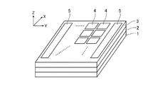
図1は、第1の実施形態に係る不揮発性半導体記憶装置の全体構成を示す斜視図である。通常のシリコン(Si)基板1(半導体基板)上に、通常用いられるプロセスにより、配線層を含むCMOS回路2が構成され、その上に複数のメモリセル部4を含む層3が形成されている。図1に示す各メモリセル部4は後述するメモリセル配列11に対応し、24nmのデザインルールで配線が形成されている。また、図1のドライバ、デコーダ及び上位ブロックを含む、通常の不揮発性半導体記憶装置における周辺回路と呼ばれている部分は、CMOS回路2に含まれている。
FIG. 1 is a perspective view showing the overall configuration of the nonvolatile semiconductor memory device according to the first embodiment. A
なお、CMOS回路2は、メモリセル部4との接続部を除き、メモリセル部4の配線よりも緩い、例えば90nmデザインルールで設計製作が行われる。各メモリセル部4の周囲には、CMOS回路2との電気的接続部(図示せず)が設けられる。これらのメモリセル部4と周辺の電気的接続部とを一単位としたブロックが、マトリックス状に配置されている。さらに、メモリセル部4を含む層3にはスルーホール(図示せず)が形成される。メモリセル部4の電気的接続部はこのスルーホールを介してCMOS回路2に接続される。メモリセル部4は、CMOS回路2によって動作が制御される。入出力部5は、CMOS回路2の入出力部と電気的な結合を有する端子を含む。これら端子も前述のスルーホールを介してCMOS回路2の入出力部に接続される。CMOS回路2がメモリセル部4の動作を制御するために必要なデータ、コマンド、アドレス等は、入出力部5を介して外部とやり取りされる。入出力部5は、メモリセル部4を含む層3の端部に形成されている。
The
以上の構成により、CMOS回路2の保護膜に相当する部分をメモリセル部4に形成される絶縁膜で兼用することが可能となる。また、本実施形態では、メモリセル部4とCMOS回路2とが積層方向(Z方向)に結合するため、チップ面積の増大を伴わずに動作時間の短縮や、同時アクセス可能なメモリセル数の大幅な増加が可能となる。なお、入出力部5は、通常の不揮発性半導体記憶装置の入出力部と同様、パッケージ工程においてリードフレームにボンディングされる。
With the above configuration, a portion corresponding to the protective film of the
次に、本実施形態に係る不揮発性半導体記憶装置の機能ブロックについて図2を参照しながら説明する。 Next, functional blocks of the nonvolatile semiconductor memory device according to the present embodiment will be described with reference to FIG.
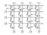
この不揮発性半導体記憶装置は、複数の行線、複数の列線、並びに、これら行線及び列線によって選択される複数のメモリセルを有するメモリセル配列11を備える。このメモリセル配列11は、図1に示すメモリセル部4に相当する。以下の説明では、通常の不揮発性半導体記憶装置にならい、行線をワード線、列線をビット線と呼ぶ。
The nonvolatile semiconductor memory device includes a
また、不揮発性半導体記憶装置は、データ消去/書き込み時に、ワード線を選択する行デコーダ12及びビット線を選択する列デコーダ13を備える。列デコーダ13は、データ消去/書き込み動作を制御するドライバを含む。
The nonvolatile semiconductor memory device also includes a
更に、不揮発性半導体記憶装置は、メモリセル配列11中のアクセス対象となるメモリセルを選択する制御回路として上位ブロック14を備える。上位ブロック14は、行デコーダ12、列デコーダ13に対して、それぞれ行アドレス、列アドレスを与える。電源15は、データ消去/書き込みの、それぞれの動作に対応した所定の電圧の組み合わせを生成し、行デコーダ12及び列13に供給する。
Further, the nonvolatile semiconductor memory device includes an
以上の機能ブロックによって、同一ワード線に接続された全てのメモリセルの一括したデータ消去/書き込みが可能になる。図1に示すCMOS回路2に、図2の行デコーダ12、列デコーダ13及び上位ブロック14などの周辺回路が設けられている。
With the above functional block, all the memory cells connected to the same word line can be erased / written collectively. The
次に、本実施形態に係る不揮発性半導体記憶装置のメモリセル配列11について図3を参照しながら説明する。
Next, the
メモリセル配列11は、複数のワード線WL及びビット線BLが交差するように配置され、これらワード線WL及びビット線BLの各交差部には、可変抵抗素子VRを有するメモリセルMCが形成されている。メモリセルMCの可変抵抗素子VRには選択素子Sが直列接続されており、この選択素子Sを介して、可変抵抗素子VRは、ワード線WL及びビット線BLから電圧の供給を受ける。
The
以上のようなメモリセル配列11の構造によれば、ワード線WL及びビット線BLは、単なるラインアンドスペースのパターンとなり、メモリセル配列11の形成に際しては、ワード線WL及びビット線BLが交差する位置関係であれば良いためズレを考慮する必要はない。つまり、メモリセルMCの位置合せ精度を極めて緩くすることができるため、不揮発性半導体記憶装置を容易に製造することができる。また、上記構造の場合、4F2の領域当たり1個のメモリセルMCを形成できるため、不揮発性半導体記憶装置の高集積化を図ることができる。
According to the structure of the
メモリセル配列11の各ワード線WLには行デコーダ12が接続されており、各ビット線BLには列デコーダ13が接続されている。また、行デコーダ12及び列デコーダ13には、電源15からデータ消去/書き込みのそれぞれの動作に対応した所定の電圧が供給される。
A
メモリセルMCへのデータ消去/書き込みは、始めに、上位ブロック14が出力する行アドレス、列アドレスに基づいて、行デコーダ12、列デコーダ13がメモリセル配列11内のアクセス対象となる選択セルMCSに接続されているワード線WL、ビット線BLを選択する。図3の場合、行デコーダ12、列デコーダ13は、それぞれワード線WL0、ビット線BL0を選択することになる。
Data erasing / writing to the memory cell MC is performed by first selecting the selected cell MC to be accessed in the
続いて、行デコーダ12は、選択ワード線WL(図3の場合、WL0)に対して選択ワード線電圧VSWを供給し、その他の非選択ワード線WL等に対して非選択ワード線電圧VUWを供給する。一方、列デコーダ13は、選択ビット線BL(図3の場合、BL0)に対して選択ビット線電圧VSBを供給し、その他の非選択ビット線BLに対して非選択ビット線電圧VUBを供給する。これら選択ワード線電圧VSW、非選択ワード線電圧VUW、選択ビット線電圧VSB及び非選択ビット線電圧VUBを適切な電圧に設定することによって、メモリセル配列11中の所定のメモリセルMCに対するアクセスができる。
Subsequently, the
次に、メモリセルMCの特性について説明する。 Next, characteristics of the memory cell MC will be described.
始めに、メモリセルMCの可変抵抗素子VRの特性について図4を参照しながら説明する。 First, the characteristics of the variable resistance element VR of the memory cell MC will be described with reference to FIG.
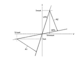
可変抵抗素子VRは、例えば、TiO2に代表される抵抗変化材を材料として形成される。この抵抗変化材は、低抵抗状態(LRS)と高抵抗状態(HRS)の少なくとも2つの抵抗値を遷移する素材である。 The variable resistance element VR is formed using, for example, a resistance change material typified by TiO 2 . This resistance change material is a material that transitions between at least two resistance values of a low resistance state (LRS) and a high resistance state (HRS).
高抵抗状態の抵抗変化材は、ある一定以上の電圧(図4の場合、負の方向に電圧Vmset以上の電圧)が印加されると、図4の矢印A1に示すように、低抵抗状態に遷移する。このような抵抗変化材の低抵抗状態から高抵抗状態への遷移をセット動作と呼ぶ。本実施形態におけるデータ書き込みは、この「セット動作」によって実現される。なお、図4では、セット動作開始時に抵抗変化材に流れている電流をIsetとして示している。 When a voltage of a certain level or higher (in the case of FIG. 4, a voltage equal to or higher than the voltage Vmset in the negative direction) is applied to the resistance change material in the high resistance state, as shown by an arrow A1 in FIG. Transition. Such a transition of the variable resistance material from the low resistance state to the high resistance state is called a set operation. Data writing in the present embodiment is realized by this “set operation”. In FIG. 4, the current flowing through the resistance change material at the start of the set operation is shown as Iset.
一方、低抵抗状態の抵抗変化材は、ある一定以上の電流(図4の場合、電流Ireset以上の電流)が流れると、図4の矢印A2に示すように、高抵抗状態に遷移する。このような抵抗変化材の低抵抗状態から高抵抗状態への遷移を「リセット動作」と呼ぶ。本実施形態におけるデータ消去は、このリセット動作によって実現される。なお、図4では、リセット動作開始時に抵抗変化材に印加される電圧をVmresetとして示している。 On the other hand, the resistance change material in the low resistance state transitions to the high resistance state as indicated by an arrow A2 in FIG. 4 when a current of a certain level or more (in the case of FIG. 4, a current equal to or greater than the current Ireset) flows. Such a transition of the variable resistance material from the low resistance state to the high resistance state is referred to as “reset operation”. Data erasure in the present embodiment is realized by this reset operation. In FIG. 4, the voltage applied to the resistance change material at the start of the reset operation is shown as Vmreset.
特に、図4に示すように、セット動作とリセット動作が、異なる極性の電圧印加でなされる可変抵抗素子VRを、「バイポーラ動作素子」と呼び、後述する選択素子Sとの組み合わせによってメモリセルMCに用いられる。 In particular, as shown in FIG. 4, a variable resistance element VR in which a set operation and a reset operation are performed by applying voltages of different polarities is referred to as a “bipolar operation element”, and is combined with a selection element S described later to form a memory cell MC. Used for.
可変抵抗素子VRは、TiO2以外にも、ZnMn2O4、HfOx、NiO、SrZrO3、Pr0.7Ca0.3MnO3、炭素等を材料とする薄膜によって構成することができる。 The variable resistance element VR can be formed of a thin film made of ZnMn 2 O 4 , HfO x , NiO, SrZrO 3 , Pr 0.7 Ca 0.3 MnO 3 , carbon, or the like, in addition to TiO 2 .
続いて、メモリセルMCの選択素子Sの特性について図5を参照しながら説明する。 Next, the characteristics of the selection element S of the memory cell MC will be described with reference to FIG.
選択素子Sは、前述の通り、可変抵抗素子VRがバイポーラ動作素子であるため、図5で示すように正負両方の極性で所定の電流を流す特性を有する必要がある。そのため、選択素子Sには、逆方向リーク電流を大きく設定したダイオードやトンネル素子等を用いる。 Since the variable resistance element VR is a bipolar operation element as described above, the selection element S needs to have a characteristic of flowing a predetermined current with both positive and negative polarities as shown in FIG. For this reason, a diode, a tunnel element, or the like with a large reverse leakage current is used as the selection element S.
選択素子Sの特性として最も重要なパラメータは、半選択セル電流IHである。ここで、半選択セル電流IHは、可変抵抗素子VRのセット動作/リセット動作に必要な電流を選択セル電流IS、この選択セル電流ISを流すためにメモリセルMCに印加される電圧をVSとすると、メモリセルMCに電圧VS/2を印加したときにメモリセルMCに流れる電流をいう。また、この半選択セル電流が流れるメモリセルMCを「半選択セル」と呼ぶ。
The most important parameter as a characteristic of the selection element S is a half-selected cell current I H. Here, the half-selected cell current I H is the variable resistor VR set operation / reset select current necessary for operating the cell current I S of the voltage applied to the memory cell MC to stream the selected cell current I S the when V S, refers to the current flowing through the memory cell MC when a voltage is applied to
次に、本実施形態に係る不揮発性半導体記憶装置のメモリセル配列11のデータ消去/書き込み時のバイアス状態について図3を参照しながら説明する。例として、ワード線WL0を選択ワード線、ビット線BL0を選択ビット線、これらワード線WL0及びビット線BL0の交差部に接続されたメモリセルMCSを選択セルとした場合のバイアス状態を示している。
Next, a bias state at the time of data erasing / writing of the
本実施形態に係る不揮発性半導体記憶装置は、データ消去/書き込みをバイポーラ動作で実行するため、選択ビット線電圧VSB、非選択ビット線VUB、選択ワード線VSW及び非選択ワード線VUWに、それぞれ所定の電圧V、0、V/2及びV/2を供給する。この場合、選択セルMCSにはおおよそ電圧Vが印加されることになる。つまり、電圧Vを図5に示す電圧VSとすれば、データ消去/書き込みに必要な電圧VSを可変抵抗素子VRに印加することができる。このとき、選択セルMCSにはビット線BL0及びワード線WL0を介してデータ消去/書き込みに必要な選択セル電流ISが流れる。 Since the nonvolatile semiconductor memory device according to the present embodiment performs data erasing / writing by a bipolar operation, a predetermined bit line voltage VSB, a non-selected bit line VUB, a selected word line VSW, and a non-selected word line VUW are respectively predetermined. Voltages V, 0, V / 2 and V / 2. In this case, approximately the voltage V will be applied to the selected cell MC S. That is, if the voltage V S that indicates the voltage V in FIG. 5, it is possible to apply a voltage V S necessary for data erase / write the variable resistance element VR. At this time, flow through the selected cell current I S required for data erase / write through the bit line BL0 and word line WL0 to the selected cell MC S.
しかし、実際には、ビット線BL及びワード線WLの配線抵抗の影響や、図3中点線矢印で示すように、半選択セルMCHを介して流れるリーク電流(半選択セル電流IH)の影響を考慮する必要がある。 However, in practice, the influence of the wiring resistance of the bit lines BL and the word line WL, and as shown in FIG. 3 dashed arrows, the leakage current flowing through the half-selected cell MC H of (half-selected cell current I H) It is necessary to consider the impact.
例えば、図6上図に示すように、選択ビット線BL0に選択ビット線電圧VSBとして電圧VS、選択ワード線WL0に選択ワード線電圧VSWとして0Vをそれぞれ供給したとする。この場合、列デコーダ13及び選択セルMCS間にある選択ビット線BL0の配線抵抗の影響によって、選択ビット線電圧VSBは低下する。また、行デコーダ12及び選択セルMCS間にある選択ワード線WL0の配線抵抗の影響によって、選択ワード線電圧VSWは上昇する。そのため選択セルMCSに印加される電圧は、データ消去/書き込みに必要な電圧VSを下回り、選択セルMCSに対する正常なデータ消去/書き込みができなくなる。特に、行デコーダ12及び列デコーダ13から遠いメモリセルMCを選択セルにした場合、ワード線WL、ビット線BLの配線抵抗の影響は大きくなる。
For example, as shown in the upper diagram of FIG. 6, it is assumed that the selected bit line BL0 is supplied with the voltage V S as the selected bit line voltage VSB, and the selected word line WL0 is supplied with 0 V as the selected word line voltage VSW. In this case, the influence of the wiring resistance of the selected bit line BL0 in between the
そこで、この問題を解決するため、図6下図に示すように、選択ビット線電圧VSB及び選択ワード線電圧VSWに対して電圧補償を施す。つまり、選択ビット線電圧VSBは電圧VSよりも更に選択ビット線BL0の配線抵抗による電圧降下分だけ高い電圧にする。また、選択ワード線電圧VSWは0Vよりも更に選択ワード線WL0の配線抵抗による電圧降下分だけ低い電圧にする。これによって、選択セルMCSに電圧VSすることができる。 In order to solve this problem, voltage compensation is performed on the selected bit line voltage VSB and the selected word line voltage VSW as shown in the lower diagram of FIG. That is, the selected bit line voltage VSB is a further voltage drop by voltage higher due to the wiring resistance of the selected bit line BL0 than the voltage V S. Further, the selected word line voltage VSW is set to a voltage lower than 0V by a voltage drop due to the wiring resistance of the selected word line WL0. This makes it possible to voltage V S to the selected cell MC S.
しかし、選択ビット線BL0に接続され、且つ、列デコーダ13から選択セルMCSの間に位置する半選択セルMCHには、電圧VS/2よりも高い選択ビット線電圧VSBが供給されることになる。この場合、半選択セルMCHを介してリーク電流が増大してしまう。更に、列デコーダ13により近い半選択セルMCHの場合、電圧VSよりも高い電圧が印加されてしまう恐れがあり、この場合、半選択セルMCHもセット動作/リセット動作してしまうディスターブの問題が生じる。この事は、選択ワード線WL0に接続された半選択セルMCHについても同様に生じる。
However, connected to the selected bit line BL0, and, in the half-selected cell MC H located between the selected cell MC S from the
そこで本実施形態に係る不揮発性半導体記憶装置では、このような配線抵抗による電圧降下やリーク電流の増大を抑制するため、メモリセル配列11を以下のように形成する。
Therefore, in the nonvolatile semiconductor memory device according to the present embodiment, the
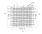
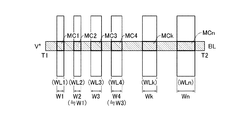
図7は、本実施形態に係る不揮発性半導体記憶装置のメモリセル配列11の形状を示す図である。図7では、本実施形態の概要の理解を容易にするため、n本(nは、2以上の整数)のワード線WLに対し、ビット線BLを1本だけ示している。図7中、ビット線BLの端部T1側(第1端部)からt番目(tは、2以上n以下の整数)のワード線をWLt、このワード線WLt及びビット線BLの交差部に配置されたメモリセルをMCtと呼ぶ。
FIG. 7 is a diagram showing the shape of the
本実施形態に係る不揮発性半導体記憶装置では、ビット線BLのワード線方向の幅(以下、「ビット線の線幅」と呼ぶ)を端部T1から端部T2(第2端部)にかけて広くしている。換言すれば、メモリセルMC2(第2部分)におけるビット線BLの線幅は、メモリセルMC1(第1部分)におけるビット線BLの線幅よりも広く、且つ、メモリセルMC3(第3部分)におけるビット線BLの線幅よりも狭くなるように形成されている。 In the nonvolatile semiconductor memory device according to this embodiment, the width of the bit line BL in the word line direction (hereinafter referred to as “bit line width”) is wide from the end T1 to the end T2 (second end). is doing. In other words, the line width of the bit line BL in the memory cell MC2 (second portion) is wider than the line width of the bit line BL in the memory cell MC1 (first portion), and the memory cell MC3 (third portion). Are formed so as to be narrower than the line width of the bit line BL.
本実施形態では、前述のようにデータ消去/書き込みをバイポーラ動作で行う。例えば、ビット線BL及びワード線WLk(kは、2以上n以下の整数)の交差部に配置されたメモリセルMCkを選択メモリセルとした場合、選択ワード線BLの端部T1側から電圧V*を供給する。また、行デコーダ12から選択ワード線WLkに0Vを供給し、それ以外の非選択ワード線WLにV/2を供給する。この時、ビット線BLは、上記の通り、図7に示す構造を有していることから、選択セルMCkの抵抗成分が、選択セルMCkよりもA端部側にあるメモリセルMC1〜MCk−1の抵抗成分よりも常に大きくなるため、電圧降下及びリーク電流が低減される。
In this embodiment, as described above, data erasing / writing is performed by a bipolar operation. For example, when the memory cell MCk arranged at the intersection of the bit line BL and the word line WLk (k is an integer of 2 or more and n or less) is the selected memory cell, the voltage V V from the end T1 side of the selected word line BL. * Supply. Further, 0 V is supplied from the
ここで、本実施形態に係る不揮発性半導体記憶装置の効果について、図17に示す比較例に係る不揮発性半導体記憶装置と比較しながら説明する。この比較例の場合、ビット線BLの線幅が一定に形成されている。 Here, the effect of the nonvolatile semiconductor memory device according to the present embodiment will be described in comparison with the nonvolatile semiconductor memory device according to the comparative example shown in FIG. In the case of this comparative example, the bit line BL has a constant line width.
また、図8は、図7及び図17を抵抗成分によってモデル化した図である。図8において、抵抗成分RLtは、ワード線WLt−1及びワード線WLt間のビット線BLの配線抵抗を示し、抵抗成分RCtは、メモリセルMCtの抵抗成分を示している。 FIG. 8 is a diagram in which FIGS. 7 and 17 are modeled by resistance components. In FIG. 8, a resistance component RLt indicates a wiring resistance of the bit line BL between the word line WLt-1 and the word line WLt, and a resistance component RCt indicates a resistance component of the memory cell MCt.
図7及び図17に示すワード線WLのビット線方向の幅(以下、「ワード線の線幅」と呼ぶ)及びビット線BLの線幅をFとする。また、図7におけるワード線WL1の中央におけるビット線BLの線幅を2/3×F、ワード線WLnの中央におけるビット線BLの線幅を4/3×Fとする。 The width of the word line WL in the bit line direction (hereinafter referred to as “word line width”) and the line width of the bit line BL shown in FIGS. Further, the line width of the bit line BL at the center of the word line WL1 in FIG. 7 is 2/3 × F, and the line width of the bit line BL at the center of the word line WLn is 4/3 × F.
ここで、比較例の場合に対する本実施形態の場合の効果を図8に示すモデルを用いて計算する。この計算の際、図8に示す抵抗成分RL及びRCは、シート抵抗を用いて計算する。また、ワード線WLの配線抵抗は考慮しない。この場合、メモリセルMC1〜MCk−1のワード線WL1〜WLk−1との接合部には電圧V/2が供給されていることとなる。更に、メモリセルMCkのビット線BLとの接合部には電圧Vが供給されており、電流は0Aだと仮定する。 Here, the effect of this embodiment relative to the case of the comparative example is calculated using the model shown in FIG. In this calculation, the resistance components RL and RC shown in FIG. 8 are calculated using the sheet resistance. Further, the wiring resistance of the word line WL is not considered. In this case, the voltage V / 2 is supplied to the junctions of the memory cells MC1 to MCk-1 with the word lines WL1 to WLk-1. Further, it is assumed that the voltage V is supplied to the junction between the memory cell MCk and the bit line BL, and the current is 0A.
この場合、ビット線BLの端部T1側の電圧V*と電流Iを求めれば、電圧差ΔV=(V*−V)が電圧降下であり、電流Iがリーク電流Ileakとなる。 In this case, if the voltage V * and the current I on the end T1 side of the bit line BL are obtained, the voltage difference ΔV = (V * −V) is a voltage drop, and the current I becomes the leak current Ileak.
図9は、比較例に対する本実施形態の電圧降下ΔV及びリーク電流Ileakの低減率を示したグラフである。このグラフは横軸がメモリセルの番号、つまり端部T1からの位置になっている。また、メモリセル数は1000となっている。 FIG. 9 is a graph showing the reduction rate of the voltage drop ΔV and the leakage current Ileak of this embodiment relative to the comparative example. In this graph, the horizontal axis is the number of the memory cell, that is, the position from the end T1. The number of memory cells is 1000.
本実施形態の電圧降下をΔV1、リーク電流I1、比較例の電圧降下をΔV2、リーク電流をI2とした場合、電圧降下ΔVの低減率は、100×(ΔV2−ΔV1)/ΔV2(%)、リーク電流Ileakの低減率は、100×(I2−I1)/I2(%)で計算することができる。 When the voltage drop of this embodiment is ΔV1, the leak current I1, the voltage drop of the comparative example is ΔV2, and the leak current is I2, the reduction rate of the voltage drop ΔV is 100 × (ΔV2−ΔV1) / ΔV2 (%), The reduction rate of the leakage current Ileak can be calculated by 100 × (I2−I1) / I2 (%).
図9に示すグラフから分かるように、端部T1から遠くなるにつれ電圧降下ΔVの低減率、リーク電流Ileakの低減率が共に上昇していることが分かる。具体的には、端部T1から最も遠い(端部T2から最も近い)メモリセルMC1000を選択セルとした場合、電圧降下ΔVの低減率として48.3%、リーク電流Ileakの低減率として30.7%の効果を得られていることが分かる。 As can be seen from the graph shown in FIG. 9, it can be seen that both the reduction rate of the voltage drop ΔV and the reduction rate of the leakage current Ileak increase as the distance from the end T1 increases. Specifically, when the memory cell MC1000 farthest from the end T1 (closest from the end T2) is the selected cell, the reduction rate of the voltage drop ΔV is 48.3%, and the reduction rate of the leakage current Ileak is 30. It turns out that the effect of 7% is acquired.
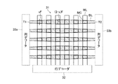
次に、図7に示す形状のビット線BLを配置させた本実施形態に係るメモリセル配列11の平面図を図10に示す。ここでは、ビット線BLの端部のうち、紙面左側の端部をT1、紙面右側の端部をT2とする。
Next, FIG. 10 shows a plan view of the
このメモリセル配列11の場合、図10上側から数えて偶数番目のビット線BLeは、端部T1において図10左側に配置された列デコーダ13を構成する第1列デコータ13aに接続されている。これら偶数番目のビット線BLeの線幅は、それぞれ端部T1から端部T2にかけて広くなるように形成されている。一方、図10上側から数えて奇数番目のビット線BLoは、端部T2において図10右側に配置された列デコーダ13を構成する第2列デコーダ13bに接続されている。これら奇数番目のビット線BLoの線幅は、それぞれ端部T2から端部T1にかけて線幅が広くなるように形成されている。
In the case of this
このように、端部T1から端部T2にかけて線幅が太くなるビット線BLoと端部T1から端部T2に掛けて線幅が細くなるビット線BLeとを互い違いに配置させることで、メモリセル配列11のサイズの増加を伴うことなく電圧降下ΔV及びリーク電流Ileakの抑制効果を得ることができる。
As described above, the bit line BLo whose line width increases from the end portion T1 to the end portion T2 and the bit line BLe which decreases from the end portion T1 to the end portion T2 are alternately arranged, thereby alternately arranging the memory cells. The effect of suppressing the voltage drop ΔV and the leakage current Ileak can be obtained without increasing the size of the
ここで、ワード線WLの線幅をF、ビット線BLのスペース幅をF、最も小さいメモリセルMCにおけるビット線BLの線幅をs×F(但し、0<s<1)、最も大きいメモリセルMCにおけるビット線BLの線幅を(2−s)×Fとした場合、ビット線BLの線幅が一定で且つワード線WL及びビット線BLのハーフピッチをFとした比較例に係るメモリセル配列と同じサイズでメモリセル配列11を形成することができる。
Here, the line width of the word line WL is F, the space width of the bit line BL is F, the line width of the bit line BL in the smallest memory cell MC is s × F (where 0 <s <1), and the largest memory. When the line width of the bit line BL in the cell MC is (2-s) × F, the memory according to the comparative example in which the line width of the bit line BL is constant and the half pitch of the word line WL and the bit line BL is F The
また、s=2/3とした場合、比較例と比べ電圧降下ΔVは最大で48.3%低減させることができる。さらに、sを小さくできる場合、つまり最小のメモリセルMCと最大のメモリセルMCのサイズの差を大きくすることができる場合、比較例と同程度のメモリセル配列のサイズを維持しながら、より電圧降下ΔVを低減させることができる。例えば、s=0.1とした場合、比較例に対する本実施形態の電圧降下ΔVの低減率を最大で93%にまですることができる。 Further, when s = 2/3, the voltage drop ΔV can be reduced by 48.3% at the maximum as compared with the comparative example. Further, when s can be reduced, that is, when the difference between the size of the smallest memory cell MC and the largest memory cell MC can be increased, the voltage of the memory cell array is maintained while maintaining the same size as the comparative example. The drop ΔV can be reduced. For example, when s = 0.1, the reduction rate of the voltage drop ΔV of the present embodiment relative to the comparative example can be reduced to 93% at the maximum.
以上、本実施形態によれば、比較例のようにビット線の線幅を一定にさせた場合よりも、電圧降下及びリーク電流の低減が図れるため、データ消去/書き込みの信頼性が高い不揮発性半導体記憶装置を提供することができる。更に、図10に示すメモリセル配列11にすることで、メモリセル配列のサイズ増大を伴うことなく、この効果を得ることができる。
As described above, according to the present embodiment, the voltage drop and the leakage current can be reduced as compared with the case where the line width of the bit line is made constant as in the comparative example, and therefore, the data erasure / write reliability is high. A semiconductor memory device can be provided. Furthermore, by using the
[第2の実施形態]
第2の実施形態に係る不揮発性半導体記憶装置は、第1の実施形態のように、端部T1から端部T2にかけて線幅が太くなるビット線BLと端部T1から端部T2に掛けて線幅が細くなるビット線BLとを互い違いに配置させることができないような場合を想定した実施形態となっている。
[Second Embodiment]
As in the first embodiment, the nonvolatile semiconductor memory device according to the second embodiment extends from the end T1 to the end T2 over the bit line BL and the end T1 to the end T2. In this embodiment, it is assumed that the bit lines BL whose line width is narrow cannot be alternately arranged.
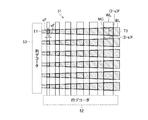
図11は、本実施形態に係る不揮発性半導体記憶装置のメモリセル配列21の平面図である。図11には、メモリセル配列21の他、行デコーダ12に相当する行デコーダ22と、列デコーダ13に相当する列デコーダ23が示されている。その他の機能ブロックについては第1の実施形態と同様である。
FIG. 11 is a plan view of the
本実施形態に係るメモリセル配列21の場合、全ビット線BLは、端部T1において図10左側に配置された列デコータ23に接続されている。また、全ビット線BLの線幅は、それぞれ端部T1から端部T2にかけて広くなるように形成されている。
In the case of the
第1の実施形態のようなビット線BLの配置ができない場合であっても、本実施形態によれば、第1の実施形態と同様、電圧低下及びリーク電流の低減を図ることができる。 Even in the case where the bit lines BL cannot be arranged as in the first embodiment, according to the present embodiment, a voltage drop and a leakage current can be reduced as in the first embodiment.
[第3の実施形態]
第1及び第2の実施形態では、ビット線の片側から選択ビット線電圧、非選択ビット線電圧を供給する場合を想定していたが、第3の実施形態は、ビット線の両側から選択ビット線電圧、非選択ビット線電圧を供給する実施形態となっている。
[Third Embodiment]
In the first and second embodiments, it is assumed that the selected bit line voltage and the non-selected bit line voltage are supplied from one side of the bit line, but the third embodiment selects the selected bit from both sides of the bit line. In this embodiment, the line voltage and the unselected bit line voltage are supplied.
図12は、本実施形態に係る不揮発性半導体記憶装置のメモリセル配列31の平面図である。図12には、メモリセル配列31の他、行デコーダ12に相当する行デコーダ32と、列デコーダ13に相当する列デコーダを構成する第1列デコーダ33a及び第2列デコーダ33bが示されている。その他の機能ブロックについては第1の実施形態と同様である。
FIG. 12 is a plan view of the
本実施形態に係るメモリセル配列31の場合、全ビット線BLには、それぞれ端部T1において図12左側に配置された第1列デコータ33a、端部T2において図12右側に配置された第2列デコーダ33bに接続されている。これらビット線BLは、それぞれ端部T1並びに端部T2から端部T1及び端部T2の中間部にかけて線幅が太くなるように形成されている。
In the case of the
本実施形態によれば、第1の実施形態と同様、電圧降下及びリーク電流の低減を図ることができる。 According to the present embodiment, a voltage drop and a leakage current can be reduced as in the first embodiment.
更に、ビット線BLの両側に列デコーダ33a、33bを配置させることで、列デコーダ33a、33b双方から最も遠いメモリセルMCは、ビット線BLの中央部に位置することになる。その結果、図17に示す比較例の場合に比べ、電圧降下を半減させることができる。
Furthermore, by disposing the
具体的には、第1の実施形態と同様、ビット線BLの最も狭い線幅をs×F、最も広い線幅を(2−s)×Fとし、s=2/3とした場合、比較例に対する本実施形態の電圧降下の低減率として約75%得ることができる。 Specifically, as in the first embodiment, the narrowest line width of the bit line BL is s × F, the widest line width is (2-s) × F, and s = 2/3. About 75% can be obtained as the reduction rate of the voltage drop of the present embodiment with respect to the example.
[第4の実施形態]
第1〜第3の実施形態では、1本のビット線BLの線幅に変化を持たせることで電圧低下及びリーク電流の低下を図っていたが、第3の実施形態は、列デコーダとの距離に応じてワード線WLの線幅を変化させる実施形態となっている。
[Fourth Embodiment]
In the first to third embodiments, the change in the line width of one bit line BL is intended to reduce the voltage and the leakage current. However, the third embodiment is different from the column decoder. In this embodiment, the line width of the word line WL is changed according to the distance.
図13は、本実施形態に係る不揮発性半導体記憶装置のメモリセル配列41の平面図である。図13には、メモリセル配列41の他、行デコーダ12に相当する行デコーダ42と、列デコーダ13に相当する列デコーダ43が示されている。その他の機能ブロックについては第1の実施形態と同様である。
FIG. 13 is a plan view of the
本実施形態に係るメモリセル配列41の場合、全ビット線BLの線幅及びスペース幅はFで一定である。一方、ワード線WLについては、各ワード線WLはそれぞれ一定の線幅で形成されているが、列デコーダ43から遠くなるにつれて線幅が一次関数的に太くなっている。例えば、図13の場合、ワード線WL´(第1行線)は、このワード線WL´よりも列デコーダ43からの距離が遠いワード線WL´´(第2行線)に比べて、線幅が狭い。これに対し、ワード線WLのスペース幅は、列デコーダ43からの距離に拘わらず一定である。
In the case of the
例えば、列デコーダ43から最も近いワード線WLの線幅をs×F(但し、0<s<1)、最も遠いワード線WLの線幅を(2−s)×F、ワード線WLのスペース幅をFとした場合、図9のグラフに示す電圧降下ΔV及びリーク電流Ileakの低減効果を得ることができる。
For example, the line width of the word line WL closest to the
以上、本実施形態によれば、第1の実施形態と同様の効果を得られる。さらに、ビット線毎の線幅及びワード線毎の線幅が一定であるため、第1〜第3の実施形態よりも配線パターンが単純であり、メモリセル配列の加工が容易である。 As described above, according to the present embodiment, the same effects as those of the first embodiment can be obtained. Furthermore, since the line width for each bit line and the line width for each word line are constant, the wiring pattern is simpler than that of the first to third embodiments, and the processing of the memory cell array is easy.
[第5の実施形態]
第5の実施形態は、第2の実施形態と第4の実施形態を組み合わせ実施形態となっている。
[Fifth Embodiment]
The fifth embodiment is a combination of the second embodiment and the fourth embodiment.
図14は、本実施形態に係る不揮発性半導体記憶装置のメモリセル配列51の平面図である。図14には、メモリセル配列51の他、行デコーダ12に相当する行デコーダ52と、列デコーダ13に相当する列デコーダ53が示されている。その他の機能ブロックについては第1の実施形態と同様である。
FIG. 14 is a plan view of the
本実施形態に係るメモリセル配列51の場合、第2の実施形態と同様、全ビット線BLは、端部T1において図14左側に配置された列デコータ53に接続されており、それぞれ端部T1から端部T2にかけて線幅が大きくなるように形成されている。また、ワード線WLは、第4の実施形態と同様、それぞれ一定の線幅で形成されているが、列デコーダ53から遠くなるにつれて線幅が一次関数的に広くなっている。これに対し、ワード線WLのスペース幅は、列デコーダ53からの距離に拘わらず一定である。
In the case of the
本実施形態によれば、第1の実施形態よりも更に、電圧降下及びリーク電流の低減を図ることができる。 According to the present embodiment, it is possible to further reduce the voltage drop and the leakage current as compared with the first embodiment.
具体的には、ビット線BLの最も狭い線幅をs×F(但し、0<s<1)、最も広い線幅を(2−s)×F、列デコーダ53から最も近いワード線WLの線幅をs×F、最も遠いワード線WLの線幅を(2−s)×Fとし、s=2/3とした場合、比較例に対する本実施形態の電圧降下の低減率として約68.6%得ることができる。 Specifically, the narrowest line width of the bit line BL is s × F (where 0 <s <1), the widest line width is (2-s) × F, and the word line WL closest to the column decoder 53 When the line width is s × F, the line width of the farthest word line WL is (2-s) × F, and s = 2/3, the reduction rate of the voltage drop of the present embodiment relative to the comparative example is about 68. 6% can be obtained.
[第6の実施形態]
第6の実施形態は第1〜第3及び第5の実施形態の変形例である。
[Sixth Embodiment]
The sixth embodiment is a modification of the first to third and fifth embodiments.
図15は、第6の実施形態に係る不揮発性半導体記憶装置のビット線の形状を示す図である。なお、図15では、図7に倣って符号を付してある。 FIG. 15 is a diagram showing the shape of the bit line of the nonvolatile semiconductor memory device according to the sixth embodiment. In FIG. 15, reference numerals are given in the same manner as FIG. 7.
第1〜第3及び第5の実施形態では、列デコーダから遠くになるにつれて次第に線幅が広くなるスロープ状のビット線が形成されていた。 In the first to third and fifth embodiments, slope-shaped bit lines are formed in which the line width gradually increases with distance from the column decoder.
これに対し、本実施形態では、図15に示すように、電圧V*が供給される端部T1(列デコーダ)側から端部T2に掛けて、段階的に線幅が広くなる階段状のビット線BLが形成されている。 On the other hand, in the present embodiment, as shown in FIG. 15, a step-like line width gradually increases from the end T1 (column decoder) side to which the voltage V * is supplied to the end T2. A bit line BL is formed.
図15の場合、ビット線BL1のワード線WL1、WL2、WL3、WL4、・・・との各交差部(第1部分、第2部分、第3部分、第4部分、・・・)における線幅をそれぞれW1、W2、W3、W4、・・・で表わすと、W1≒W2<W3≒W4<・・・となるように、ワード線WL2本毎に線幅が広くなる階段状のビット線BLが形成されている。 In the case of FIG. 15, the lines at the intersections (first part, second part, third part, fourth part,...) Of the bit line BL1 with the word lines WL1, WL2, WL3, WL4,. When the widths are expressed as W1, W2, W3, W4,..., Stepwise bit lines whose line width is widened every two word lines WL so that W1≈W2 <W3≈W4 <. BL is formed.
このように第1〜第3及び第5の実施形態において、スロープ状ではなく、段階的に線幅が変化する階段状のビット線を形成した場合であっても、第1〜第3及び第5の実施形態と同様の効果を得ることができる。 As described above, in the first to third and fifth embodiments, even if the stepped bit line whose line width changes stepwise is formed instead of the slope shape, the first to third and fifth embodiments are formed. The same effect as that of the fifth embodiment can be obtained.
なお、本実施形態は、後述する第7の実施形態と共に第5の実施形態に適用することも可能である。 This embodiment can also be applied to the fifth embodiment together with the seventh embodiment described later.
[第7の実施形態]
第7の実施形態は第4及び第5の実施形態の変形例である。
[Seventh Embodiment]
The seventh embodiment is a modification of the fourth and fifth embodiments.
図16は、第7の実施形態に係る不揮発性半導体記憶装置のワード線の形状を示す図である。なお、図16では、図7に倣って符号を付してある。 FIG. 16 is a diagram showing the shape of the word line of the nonvolatile semiconductor memory device according to the seventh embodiment. In FIG. 16, reference numerals are given in the same manner as FIG. 7.
第4及び第5の実施形態では、列デコーダから遠くにつれて1本毎に線幅が広くなるようにワード線が形成されていた。 In the fourth and fifth embodiments, the word lines are formed so that the line width increases for each line as it is far from the column decoder.
これに対し、本実施形態では、図16に示すように、電圧V*が供給される端部T1(列デコーダ)側から端部T2に掛けて、複数本のグループ毎に線幅が広くなるようにワード線WLが形成されている。 On the other hand, in this embodiment, as shown in FIG. 16, the line width is widened for each of a plurality of groups from the end T1 (column decoder) side to which the voltage V * is supplied to the end T2. Thus, the word line WL is formed.
図16の場合、ワード線WL1(第1行線)、WL2(第1行線)、WL3(第2行線)、WL4(第2行線)、・・・の線幅をそれぞれW1、W2、W3、W4、・・・で表わすと、W1≒W2<W3≒W4<・・・となるように、2本のグループ毎にワード線WLの線幅が広くなるように形成されている。 In the case of FIG. 16, the line widths of the word lines WL1 (first row line), WL2 (first row line), WL3 (second row line), WL4 (second row line),. , W3, W4,..., The width of the word line WL is increased every two groups so that W1≈W2 <W3≈W4 <.
このように第4及び第5の実施形態において、ワード線の線幅を1本毎ではなく、複数本のグループ毎に変化させた場合であっても、第4及び第5の実施形態と同様の効果を得ることができる。 As described above, in the fourth and fifth embodiments, even when the line width of the word line is changed for each of a plurality of groups instead of for each one, the same as in the fourth and fifth embodiments. The effect of can be obtained.
なお、本実施形態は、第6の実施形態と共に第5の実施形態に適用することも可能である。 Note that this embodiment can also be applied to the fifth embodiment together with the sixth embodiment.
[その他]
以上、本発明のいくつかの実施形態を説明したが、これらの実施形態は、例として提示したものであり、発明の範囲を限定することは意図していない。これら新規な実施形態は、その他の様々な形態で実施されることが可能であり、発明の要旨を逸脱しない範囲で、種々の省略、置き換え、変更を行うことができる。これら実施形態やその変形は、発明の範囲や要旨に含まれるとともに、特許請求の範囲に記載された発明とその均等の範囲に含まれる。
[Others]
As mentioned above, although some embodiment of this invention was described, these embodiment is shown as an example and is not intending limiting the range of invention. These novel embodiments can be implemented in various other forms, and various omissions, replacements, and changes can be made without departing from the scope of the invention. These embodiments and modifications thereof are included in the scope and gist of the invention, and are included in the invention described in the claims and the equivalents thereof.
例えば、第1〜第7の実施形態において、行線であるワード線及び行デコーダと列線であるビット線及び列デコーダを入れ替えた場合であっても、各実施形態と同様の効果を得ることができる。 For example, in the first to seventh embodiments, even when the word lines and row decoders as row lines are replaced with the bit lines and column decoders as column lines, the same effects as those of the embodiments can be obtained. Can do.
1・・・シリコン基板、2・・・CMOS回路、3・・・メモリセル部を含む層、4・・・メモリセル部、5・・・入出力部、11、21、31、41、51・・・メモリセル配列、12、22、32、42、52・・・行デコーダ、13、23、33、43、53・・・列デコーダ、14・・・上位ブロック、15・・・電源。
DESCRIPTION OF
Claims (7)
前記列線を介して前記メモリセルに対して前記可変抵抗素子の状態遷移に必要な電圧を供給する前記列線の第1端部及び第2端部の少なくとも一方に配置された列デコーダと
を備え、
前記列線は、第1部分、前記第1部分よりも前記列デコーダから遠い第2部分及び前記第2部分よりも前記列デコーダから遠い第3部分を有し、前記第2部分の前記行方向の線幅は、前記第1部分の前記行方向の線幅と同等又はより広く、且つ、前記第3部分の前記行方向の線幅よりも狭い
ことを特徴とする不揮発性半導体記憶装置。 A plurality of memories including a plurality of column lines extending in the column direction, a plurality of row lines extending in the row direction intersecting with the column direction, and variable resistance elements arranged at intersections of the plurality of column lines and the row lines A memory cell array having cells;
A column decoder disposed at at least one of a first end and a second end of the column line for supplying a voltage necessary for the state transition of the variable resistance element to the memory cell via the column line; Prepared,
The column line has a first portion, a second portion farther from the column decoder than the first portion, and a third portion farther from the column decoder than the second portion, and the row direction of the second portion The non-volatile semiconductor memory device is characterized in that the line width of the first portion is equal to or wider than the line width of the first portion in the row direction and narrower than the line width of the third portion in the row direction.
前記複数の列線の一部は第1列線であり、他の一部は第2列線であり、
前記第1列デコーダは、前記第1列線の前記第1端部に配置され、
前記第2列デコーダは、前記第2列線の前記第2端部に配置され、
前記第1列線は、前記第1端部から前記第2端部にかけて前記行方向の線幅が広くなり、
前記第2列線は、前記第2端部から前記第1端部にかけて前記行方向の線幅が広くなる
ことを特徴とする請求項1記載の不揮発性半導体記憶装置。 The column decoder comprises a first column decoder and a second column decoder,
A part of the plurality of column lines is a first column line, and another part is a second column line;
The first column decoder is disposed at the first end of the first column line;
The second column decoder is disposed at the second end of the second column line;
The first column line has a wider line width in the row direction from the first end to the second end,
The nonvolatile semiconductor memory device according to claim 1, wherein the second column line has a line width in the row direction that increases from the second end portion to the first end portion.
ことを特徴とする請求項2記載の不揮発性半導体記憶装置。 The nonvolatile semiconductor memory device according to claim 2, wherein the first column lines and the second column lines are alternately arranged in the row direction.
前記複数の列線は、前記第1端部から前記第2端部にかけて前記行方向の線幅が広くなる
ことを特徴とする請求項1記載の不揮発性半導体記憶装置。 The column decoder is disposed at the first end of the plurality of column lines;
The nonvolatile semiconductor memory device according to claim 1, wherein the plurality of column lines have a line width in the row direction that increases from the first end to the second end.
前記第1列デコーダ及び前記第2列デコーダは、それぞれ前記列線の前記第1端部及び前記第2端部に配置され、
前記列線は、前記第1端部並びに前記第2端部から前記第1端部及び前記第2端部の中間部にかけて前記行方向の線幅が広くなる
ことを特徴とする請求項1記載の不揮発性半導体記憶装置。 The column decoder comprises a first column decoder and a second column decoder,
The first column decoder and the second column decoder are disposed at the first end and the second end of the column line, respectively.
2. The line width in the row direction increases from the first end portion and the second end portion to an intermediate portion between the first end portion and the second end portion. Nonvolatile semiconductor memory device.
ことを特徴とする請求項1又は4記載の不揮発性半導体記憶装置。 The line width in the column direction of the other row line near the column decoder is wider than the line width in the column direction of the predetermined row line far from the column decoder. 5. The nonvolatile semiconductor memory device according to 4.
前記列線を介して前記メモリセルに対して前記可変抵抗素子の状態遷移に必要な電圧を供給する前記列線の第1端部及び第2端部の少なくとも一方に配置された列デコーダと
を備え、
前記複数の行線の一部は第1行線であり、他の一部は第2行線であり、前記第2行線は、前記第1行線よりも前記デコーダから遠く、且つ、前記1行線よりも前記列方向の線幅が広い
ことを特徴とする不揮発性半導体記憶装置。 A plurality of memories including a plurality of column lines extending in the column direction, a plurality of row lines extending in the row direction intersecting with the column direction, and variable resistance elements arranged at intersections of the plurality of column lines and the row lines A memory cell array having cells;
A column decoder disposed at at least one of a first end and a second end of the column line for supplying a voltage necessary for the state transition of the variable resistance element to the memory cell via the column line; Prepared,
A part of the plurality of row lines is a first row line, another part is a second row line, the second row line is farther from the decoder than the first row line, and the A non-volatile semiconductor memory device, wherein a line width in the column direction is wider than one row line.
Priority Applications (1)
| Application Number | Priority Date | Filing Date | Title |
|---|---|---|---|
| JP2011023635A JP2012164384A (en) | 2011-02-07 | 2011-02-07 | Non-volatile semiconductor memory device |
Applications Claiming Priority (1)
| Application Number | Priority Date | Filing Date | Title |
|---|---|---|---|
| JP2011023635A JP2012164384A (en) | 2011-02-07 | 2011-02-07 | Non-volatile semiconductor memory device |
Publications (1)
| Publication Number | Publication Date |
|---|---|
| JP2012164384A true JP2012164384A (en) | 2012-08-30 |
Family
ID=46843632
Family Applications (1)
| Application Number | Title | Priority Date | Filing Date |
|---|---|---|---|
| JP2011023635A Withdrawn JP2012164384A (en) | 2011-02-07 | 2011-02-07 | Non-volatile semiconductor memory device |
Country Status (1)
| Country | Link |
|---|---|
| JP (1) | JP2012164384A (en) |
Cited By (1)
| Publication number | Priority date | Publication date | Assignee | Title |
|---|---|---|---|---|
| JP2021536600A (en) * | 2018-08-21 | 2021-12-27 | シリコン ストーリッジ テクノロージー インコーポレイテッドSilicon Storage Technology, Inc. | Analog neural memory system for deep learning neural networks with multiple vector matrix multiplication arrays and shared components |
-
2011
- 2011-02-07 JP JP2011023635A patent/JP2012164384A/en not_active Withdrawn
Cited By (2)
| Publication number | Priority date | Publication date | Assignee | Title |
|---|---|---|---|---|
| JP2021536600A (en) * | 2018-08-21 | 2021-12-27 | シリコン ストーリッジ テクノロージー インコーポレイテッドSilicon Storage Technology, Inc. | Analog neural memory system for deep learning neural networks with multiple vector matrix multiplication arrays and shared components |
| JP7399153B2 (en) | 2018-08-21 | 2023-12-15 | シリコン ストーリッジ テクノロージー インコーポレイテッド | Analog neural memory system for deep learning neural networks with multiple vector matrix multiplication arrays and shared components |
Similar Documents
| Publication | Publication Date | Title |
|---|---|---|
| TWI508079B (en) | Nonvolatile semiconductor memory device and method for resetting it | |
| JP4309877B2 (en) | Semiconductor memory device | |
| JP6433854B2 (en) | Semiconductor memory device | |
| JP5032621B2 (en) | Nonvolatile semiconductor memory and manufacturing method thereof | |
| KR100855585B1 (en) | Resistive random access memory having common source line | |
| KR100827706B1 (en) | Semiconductor memory device and method for biasing of dummy line therefore | |
| JP5132703B2 (en) | Nonvolatile semiconductor memory device | |
| JP2007164925A (en) | Nonvolatile semiconductor memory device | |
| JP2013004143A (en) | Nonvolatile semiconductor memory device | |
| JP2015103271A (en) | Memory device and method of controlling memory device | |
| KR101595168B1 (en) | Semiconductor memory device | |
| JP5209013B2 (en) | Nonvolatile semiconductor memory device | |
| KR20200008998A (en) | Memory device and control method of the memory device | |
| JP5988061B2 (en) | Nonvolatile semiconductor memory device | |
| US11257536B2 (en) | Semiconductor storage device and control method thereof | |
| JP2012164384A (en) | Non-volatile semiconductor memory device | |
| US20190189205A1 (en) | Resistive memory apparatus and line selection circuit thereof | |
| JP2013200936A (en) | Semiconductor memory device and method for controlling the same | |
| JP2018147924A (en) | Semiconductor memory device | |
| US9478283B2 (en) | Nonvolatile semiconductor storage device having improved reading and writing speed characteristics | |
| JP5665717B2 (en) | Nonvolatile semiconductor memory device |
Legal Events
| Date | Code | Title | Description |
|---|---|---|---|
| RD01 | Notification of change of attorney |
Free format text: JAPANESE INTERMEDIATE CODE: A7421 Effective date: 20130221 |
|
| A300 | Application deemed to be withdrawn because no request for examination was validly filed |
Free format text: JAPANESE INTERMEDIATE CODE: A300 Effective date: 20140513 |