JP2012160928A - Load drive circuit - Google Patents
Load drive circuit Download PDFInfo
- Publication number
- JP2012160928A JP2012160928A JP2011019425A JP2011019425A JP2012160928A JP 2012160928 A JP2012160928 A JP 2012160928A JP 2011019425 A JP2011019425 A JP 2011019425A JP 2011019425 A JP2011019425 A JP 2011019425A JP 2012160928 A JP2012160928 A JP 2012160928A
- Authority
- JP
- Japan
- Prior art keywords
- voltage
- current
- mos transistor
- output
- load
- Prior art date
- Legal status (The legal status is an assumption and is not a legal conclusion. Google has not performed a legal analysis and makes no representation as to the accuracy of the status listed.)
- Withdrawn
Links
Images


Abstract
Description
本発明は、負荷駆動回路に関する。特に、ハイサイドスイッチとして機能する出力トランジスタに対する過電流保護機能を備えた負荷駆動回路に関する。 The present invention relates to a load driving circuit. In particular, the present invention relates to a load driving circuit having an overcurrent protection function for an output transistor that functions as a high-side switch.
負荷駆動回路では、トランジスタをハイサイドスイッチとして用いることが多い。ここで、特許文献1において、負荷が短絡したことにより出力トランジスタに過電流が流れ、出力トランジスタが熱破壊してしまうことを、出力トランジスタに流れる電流を制限することにより防止する駆動回路が開示されている。
In a load driving circuit, a transistor is often used as a high-side switch. Here,
しかし、特許文献1で開示された負荷駆動回路では、電流制限値が単一に固定されているため低電圧領域では過剰な電流制限となり、広い負荷条件に適用できない。そこで、特許文献2において、電流制限値を単一に固定せず、出力電圧に応じて変化させ、適用可能な負荷条件を拡大する回路が開示されている。
However, in the load driving circuit disclosed in
以下の分析は、本発明の観点からなされたものである。 The following analysis has been made from the viewpoint of the present invention.
特許文献2で開示された電流制限特性を2段階とする負荷駆動回路の電力について検討する。電流制限特性を2段階とする負荷駆動回路では、電源電圧を2等分した電圧ポイントにおいて、最大電流制限値を2等分した電流値だけ変化させると、高・低の両電圧領域において概ね均等な最大制限電力を得ることができる。
The power of the load driving circuit having the current limiting characteristic disclosed in
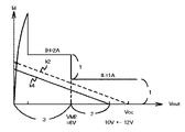
図2は、2段階の電流制限を行なう負荷駆動回路における電流−電圧特性を示す図である。例えば、図2に示すように、負荷駆動回路の電流をILimit1(最大電流制限)とILimit2に制限する場合に、電源電圧Vccの1/2の電圧ポイントであるVaにおいてILimit1とILimit2が切り替わるよう設定する。同時に、電流ILimit1とILimit2の比を1:1に設定する。 FIG. 2 is a diagram showing current-voltage characteristics in a load driving circuit that performs two-stage current limiting. For example, as shown in FIG. 2, when the current of the load drive circuit is limited to ILimit1 (maximum current limit) and ILimit2, ILimit1 and ILimit2 are set to switch at Va, which is a voltage point ½ of the power supply voltage Vcc. To do. At the same time, the ratio of the currents ILimit1 and ILimit2 is set to 1: 1.
上記の電圧及び電流に具体的な数字を当てはめ電力を計算する。ここでは、Vcc=12V、Va=6V、ILimit1=2A、ILimit2=1とする。Vaより小さい領域(図2の低電圧領域)の電力は6V×2A=12Wと計算でき、Va以上かつVcc以下の領域(図2の高電圧領域)の電力は12V×1A=12Wと計算できる。 The power is calculated by applying specific numbers to the above voltage and current. Here, Vcc = 12V, Va = 6V, ILimit1 = 2A, and ILimit2 = 1. The power in the region smaller than Va (the low voltage region in FIG. 2) can be calculated as 6V × 2A = 12 W, and the power in the region above Va and not higher than Vcc (the high voltage region in FIG. 2) can be calculated as 12 V × 1A = 12 W. .
しかし、このように最大制限電力のバランスを考慮して、最大電流制限値(ILimit1)や切り替え電圧ポイント(Va)を設定したとしても、当初の設計と異なる電源電圧条件で負荷駆動回路が使用された場合、負荷特性と電流制限特性との適正な関係(バランスが取れた状態)が、くずれてしまう問題が存在する(詳細な説明は後述する)。即ち、特許文献2で開示された負荷駆動回路は、複数の電源電圧条件に対する電流制限特性の追従性に関する配慮はされていない。
However, even if the maximum current limit value (ILimit1) and the switching voltage point (Va) are set in consideration of the balance of the maximum limit power as described above, the load driving circuit is used under a power supply voltage condition different from the original design. In this case, there is a problem that an appropriate relationship (a balanced state) between the load characteristic and the current limiting characteristic is lost (detailed description will be described later). That is, the load drive circuit disclosed in
以上のとおり、従来技術には、解決すべき問題点が存在する。 As described above, there are problems to be solved in the prior art.
本発明の一側面において、複数の電源電圧条件に対して電流制限特性が追従し、負荷特性に適した電流制限を行なう負荷駆動回路が、望まれる。 In one aspect of the present invention, a load driving circuit is desired in which a current limiting characteristic follows a plurality of power supply voltage conditions and performs a current limiting suitable for the load characteristic.
本発明の第1の視点によれば、電源及び負荷に接続された出力MOSトランジスタと、前記出力MOSトランジスタの出力電圧に応じて、前記出力MOSトランジスタに流れる出力電流を複数段階の制限電流に制限すると共に、前記制限電流が切り替わる際の出力電圧を電源電圧の変化に基づいて切り替える電流制限値切り替え回路と、を備える負荷駆動回路が提供される。 According to the first aspect of the present invention, an output MOS transistor connected to a power source and a load, and an output current flowing through the output MOS transistor is limited to a plurality of stages of limited currents according to an output voltage of the output MOS transistor. In addition, a load drive circuit is provided that includes a current limit value switching circuit that switches an output voltage when the limit current is switched based on a change in power supply voltage.
本発明の視点によれば、複数の電源電圧条件に対して電流制限特性が追従し、負荷特性に適した電流制限を行なう負荷駆動回路が、提供される。 According to an aspect of the present invention, a load driving circuit is provided in which current limiting characteristics follow a plurality of power supply voltage conditions and current limiting suitable for load characteristics is performed.
初めに、図1を用いて実施形態の概要について説明する。なお、この概要に付記した図面参照符号は、理解を助けるための一例として各要素に便宜上付記したものであり、本発明を図示の態様に限定することを意図するものではない。 First, the outline of the embodiment will be described with reference to FIG. Note that the reference numerals of the drawings attached to this summary are attached to the respective elements for convenience as an example for facilitating understanding, and are not intended to limit the present invention to the illustrated embodiment.
上述のように、最大制限電力のバランスを考慮して、最大電流制限値や切り替え電圧ポイントを設定したとしても、想定された電源電圧と異なる電圧条件で負荷駆動回路を使用すると負荷特性と電流制限特性との適正な関係がくずれてしまう。そのため、複数の電源電圧条件に対して電流制限特性が追従し、全体として負荷特性に適した電流制限を行なう負荷駆動回路が必要となる。 As described above, even if the maximum current limit value and switching voltage point are set in consideration of the balance between the maximum limit power and the load drive circuit is used under a voltage condition different from the assumed power supply voltage, the load characteristics and current limit The proper relationship with the characteristics will be lost. Therefore, there is a need for a load driving circuit in which the current limiting characteristic follows a plurality of power supply voltage conditions and performs current limiting suitable for the load characteristic as a whole.
そこで、図1に示す負荷駆動回路を提供する。図1に示す負荷駆動回路は、電源及び負荷に接続された出力MOSトランジスタと、出力MOSトランジスタの出力電圧に応じて、出力MOSトランジスタに流れる出力電流を複数段階の制限電流に制限すると共に、制限電流が切り替わる際の出力電圧を電源電圧の変化に基づいて切り替える電流制限値切り替え回路と、を備える。 Therefore, the load driving circuit shown in FIG. 1 is provided. The load driving circuit shown in FIG. 1 limits the output current flowing through the output MOS transistor to a plurality of stages of limiting currents according to the output MOS transistors connected to the power source and the load, and the output voltage of the output MOS transistors. A current limit value switching circuit that switches an output voltage when the current is switched based on a change in the power supply voltage.
図1に示す負荷駆動回路は、複数の異なる電流制限値を用いて段階的に電流制限を行なうため、過剰な電流制限となることを妨げ、負荷条件の拡大を図ることができる。さらに、電流制限値の切り替えを電源電圧に対応させて行なうため、当初の電源電圧条件とは異なる電源電圧で使用したとしても、電流制限特性が電源電圧の変動に追従し、負荷特性に適した電流制限を行なうことができる。 Since the load driving circuit shown in FIG. 1 performs current limitation step by step using a plurality of different current limit values, it is possible to prevent excessive current limitation and to expand load conditions. Furthermore, since the current limit value is switched according to the power supply voltage, even if it is used at a power supply voltage different from the original power supply voltage condition, the current limit characteristics follow the fluctuation of the power supply voltage and are suitable for the load characteristics. Current limiting can be performed.
その結果、特定の電源電圧に基づいて設計した負荷駆動回路を当初の設計とは異なる電源電圧で使用したとしても、負荷駆動回路の設計及び評価を再び行う必要がなくなる。設計及び評価を行う必要がなくなれば、負荷駆動回路の汎用性が高まると共に、負荷駆動回路の設計コストを低減させることが可能になる。 As a result, even if a load drive circuit designed based on a specific power supply voltage is used at a power supply voltage different from the original design, it is not necessary to design and evaluate the load drive circuit again. If it is not necessary to perform design and evaluation, the versatility of the load drive circuit is enhanced and the design cost of the load drive circuit can be reduced.
次に、特許文献1で開示された負荷駆動回路を、図3を用いて説明する。図3に示す負荷駆動回路10は、電源端子Pinと、入力端子Inと、出力端子Outとを備え、MOSトランジスタM1乃至M3と、抵抗R1及びR2から構成されている。さらに、チャージポンプ回路CPが入力端子Inと接続され、電源端子Pinは電源に接続、出力端子Outは接地された外部の負荷LDに接続されている。なお、以降の説明においてMOSトランジスタはnチャンネル型MOSトランジスタを表すものとする。
Next, the load drive circuit disclosed in
MOSトランジスタM1は出力トランジスタであり、MOSトランジスタM2は電流検出用のトランジスタである。出力電流はIdとし、電流検出用MOSトランジスタM2に流れる電流をセンス電流Isとする。電圧Vdは、出力MOSトランジスタM1のドレイン・ソース間電圧、Vsはセンス電圧(抵抗R2の両端電圧)、Vinは入力電圧、Vccは電源電圧、Voutは出力電圧とする。 The MOS transistor M1 is an output transistor, and the MOS transistor M2 is a current detection transistor. The output current is Id, and the current flowing through the current detection MOS transistor M2 is the sense current Is. The voltage Vd is the drain-source voltage of the output MOS transistor M1, Vs is the sense voltage (the voltage across the resistor R2), Vin is the input voltage, Vcc is the power supply voltage, and Vout is the output voltage.
図3に示すように、出力MOSトランジスタM1は、負荷LDに対してハイサイドスイッチとして機能し、ドレインは電源端子Pinに接続され、ソースは負荷LDに接続されている。出力MOSトランジスタM1のゲートは、抵抗R1を介してチャージポンプ回路CPに接続されている。 As shown in FIG. 3, the output MOS transistor M1 functions as a high-side switch for the load LD, the drain is connected to the power supply terminal Pin, and the source is connected to the load LD. The gate of the output MOS transistor M1 is connected to the charge pump circuit CP via the resistor R1.
負荷駆動回路10において、電流検出用MOSトランジスタM2及びMOSトランジスタM3、抵抗R2により過電流保護回路を構成する。電流検出用MOSトランジスタM2のゲートは出力MOSトランジスタM1のゲートと接続され、電流検出用MOSトランジスタM2のドレインは出力MOSトランジスタM1のドレインと接続されている。電流検出用MOSトランジスタM2のソースは、MOSトランジスタM3のゲート及び抵抗R2に共通接続されている。MOSトランジスタM3のゲートは電流検出用MOSトランジスタM2のソース及び抵抗R2に接続され、ドレインは出力MOSトランジスタM1及び電流検出用MOSトランジスタM2のゲートと共通接続され、ソースは抵抗R2に接続されると共に出力端子Out(負荷LD)と接続されている。
In the
出力電流Idとセンス電流Isは、出力MOSトランジスタM1と電流検出用MOSトランジスタM2のセルサイズ比に対応した電流比となる。電流検出用MOSトランジスタM2を使用することで、出力電流Idを精度よく検出することができる。電流検出用MOSトランジスタM2のソースと出力端子Out間に接続された抵抗R2は、センス電流Isをセンス電圧Vsに変換する。 The output current Id and the sense current Is have a current ratio corresponding to the cell size ratio of the output MOS transistor M1 and the current detection MOS transistor M2. By using the current detection MOS transistor M2, the output current Id can be detected with high accuracy. A resistor R2 connected between the source of the current detection MOS transistor M2 and the output terminal Out converts the sense current Is into a sense voltage Vs.
センス電圧VsがMOSトランジスタM3の閾値電圧Vt3以上になるとMOSトランジスタM3がオン状態となり、出力MOSトランジスタM1のゲート電圧を低下させる。なお、以降の説明において、各トランジスタの閾値電圧はトランジスタの符号番号を用いて表現する。例えば、出力MOSトランジスタM1の閾値電圧はVt1と表現する。 When the sense voltage Vs becomes equal to or higher than the threshold voltage Vt3 of the MOS transistor M3, the MOS transistor M3 is turned on to lower the gate voltage of the output MOS transistor M1. In the following description, the threshold voltage of each transistor is expressed using a transistor code number. For example, the threshold voltage of the output MOS transistor M1 is expressed as Vt1.
出力MOSトランジスタM1のゲート電圧が低下すると、出力電流Idは制限される。この際の動作を、図4を用いて説明する。 When the gate voltage of the output MOS transistor M1 decreases, the output current Id is limited. The operation at this time will be described with reference to FIG.
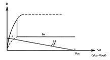
図4は、出力MOSトランジスタM1のドレイン電圧Vd(Vcc−Voutに相当)と出力電流Idの関係を示す図である。図4の縦軸に出力電流Id、横軸にドレイン電圧Vdをそれぞれ示す。図4のk1は負荷特性を示す。 FIG. 4 is a diagram showing the relationship between the drain voltage Vd (corresponding to Vcc−Vout) of the output MOS transistor M1 and the output current Id. In FIG. 4, the vertical axis represents the output current Id, and the horizontal axis represents the drain voltage Vd. In FIG. 4, k1 indicates a load characteristic.
図4から分かるように、負荷特性k1は、横軸とVccで交わる負勾配を有する直線となる。また、出力MOSトランジスタM1の電流−電圧特性はNMOSトランジスタの基本トランジスタ特性に相当し、両者の交点aが出力MOSトランジスタM1の動作点となる。図5は、図4に電流制限値(以下、Imと呼ぶ)を重ねた図である。図5に示すように、出力MOSトランジスタM1の電流能力を有効に利用するため、電流制限値Imは負荷特性k1と交差しないように設定される。 As can be seen from FIG. 4, the load characteristic k1 is a straight line having a negative gradient that intersects the horizontal axis and Vcc. The current-voltage characteristic of the output MOS transistor M1 corresponds to the basic transistor characteristic of the NMOS transistor, and the intersection point a between them is the operating point of the output MOS transistor M1. FIG. 5 is a diagram in which a current limit value (hereinafter referred to as Im) is superimposed on FIG. As shown in FIG. 5, in order to effectively use the current capability of the output MOS transistor M1, the current limit value Im is set so as not to cross the load characteristic k1.
ここで、負荷LDの短絡が発生したとすると、出力電流Idの増加に比例し、センス電流Isも増加する。センス電流Isが増加すれば、センス電圧Vsも増加し、センス電圧VsはいずれMOSトランジスタM3の閾値電圧Vt3に到達する。センス電圧Vsが、MOSトランジスタM3の閾値電圧Vt3以上になるとMOSトランジスタM3はオン状態になり、出力MOSトランジスタM1のゲート電圧は所定の電圧(以下、Vgcと呼ぶ)まで低下する。その結果、出力電流Idは電流制限値Imに制限され、過電流から保護される。 Here, if a short circuit of the load LD occurs, the sense current Is also increases in proportion to the increase in the output current Id. If the sense current Is increases, the sense voltage Vs also increases, and the sense voltage Vs eventually reaches the threshold voltage Vt3 of the MOS transistor M3. When the sense voltage Vs becomes equal to or higher than the threshold voltage Vt3 of the MOS transistor M3, the MOS transistor M3 is turned on, and the gate voltage of the output MOS transistor M1 decreases to a predetermined voltage (hereinafter referred to as Vgc). As a result, the output current Id is limited to the current limit value Im, and is protected from overcurrent.
続いて、特許文献2で開示された負荷駆動回路について説明する。図6は、特許文献2の図1で開示された負荷駆動回路の回路図である。負荷駆動回路20は、電圧検出回路21と、電圧クランプ回路22と、出力MOSトランジスタM4と、抵抗12から構成されている。
Next, the load drive circuit disclosed in
負荷駆動回路20の出力MOSトランジスタM4はローサイドスイッチとして動作し、出力端子Outは負荷LDに接続されている。負荷駆動回路20に対する入力は入力端子InP及びInNで受け付け、負荷駆動回路20はGnd端子を介して接地されている。
The output MOS transistor M4 of the
負荷駆動回路20では、出力電圧Voutのレベルに応じてクランプ電圧を変化させることで、電流制限値を2段階に切り替え可能となっている。その結果、負荷駆動回路20は電流制限による過剰な制約を緩和して、より広い範囲の負荷条件に適用可能としている。
In the
負荷駆動回路20においては、電圧検出回路21と電圧クランプ回路22により、過電流保護回路を構成する。電圧検出回路21は、出力端子Outと接地端子Gnd間に接続され、出力MOSトランジスタM4に印加される電圧を検出する。電圧クランプ回路22は、出力MOSトランジスタM4のゲートと接地端子Gnd間に接続され、異なる2つのクランプ電圧を生成する。電圧クランプ回路22の出力(出力MOSトランジスタM4のゲートと抵抗R3の接続点)をノードS1とする。さらに、電圧検出回路21は、MOSトランジスタM5乃至M9と、抵抗R6乃至R11から構成され、電圧クランプ回路22は、MOSトランジスタM10と、抵抗R3乃至R5から構成されている。なお、抵抗R3乃至R12の抵抗値を、それぞれr3乃至r12と表記して以下の説明を行なう。
In the
次に、負荷駆動回路20の動作を説明する。図7乃至図9は、負荷駆動回路20の各MOSトランジスタのオン/オフ状態を出力電圧の範囲に応じて併記した図である。図10は、入力電圧と出力電圧の関係を示すタイミングチャートであり、図11は負荷特性と電流制限特性の関係を示す電流−電圧特性図である。これらの図を用いて、負荷駆動回路20の動作を説明する。
Next, the operation of the
図10に示すように、時刻t1までは入力電圧VinはLレベルであり、出力MOSトランジスタM4はオフ状態である。従って、出力電流Idは流れず、出力電圧Voutは電源電圧Vccとなる。 As shown in FIG. 10, until time t1, the input voltage Vin is at the L level, and the output MOS transistor M4 is in the off state. Therefore, the output current Id does not flow, and the output voltage Vout becomes the power supply voltage Vcc.
次に、時刻t1に入力信号VinがHレベルに遷移すると、出力MOSトランジスタM4は導通を始める。その際に、MOSトランジスタM5のゲートには式(1)の電圧が印加される。
![]()
![]()
一方、MOSトランジスタM8のゲートには、式(2)で表せる電圧が印加される。
![]()
![]()
ここで、VM1はVM2より小さく(VM1<VM2)、閾値電圧Vt5と閾値電圧Vt8は等しいものとする。このとき、ノードS1から出力される電圧クランプ回路22の出力電圧であるVGS1は式(3)で表せる電圧となる。
![]()
![]()
さらに、出力電流Idが増加することで出力電圧Voutが低下し、出力電圧Voutが、VM1≦Vout<VM2の範囲内となると、図8に示すように、MOSトランジスタM8がオフ状態、MOSトランジスタM9がオン状態となり、抵抗R5は回避(シャント)される。このときの電圧クランプ回路22の出力電圧VGS2は、式(4)で表せる電圧となる。なお、VGS2>VGS1である。
![]()
![]()
さらに、出力電流Idが増加することで出力電圧Voutが低下し、出力電圧Voutが、Vout<VM1となると、図9に示すようにMOSトランジスタM5がオフ状態、MOSトランジスタM6がオン状態、MOSトランジスタM7がオフ状態となる。それに伴って、MOSトランジスタM10がオフ状態になり、電圧クランプ回路22は不活性となる。電圧クランプ回路22が不活性になると、出力MOSトランジスタM4のゲートには、式(5)で表される電圧が印加される。
![]()
![]()
その後、負荷LDが短絡すると、出力電圧Voutは、ほぼ電源電圧Vccに等しくなる。その結果、電圧検出回路21はMOSトランジスタM7をオン状態にして電流制限を活性化すると共に、MOSトランジスタM9をオフ状態にして、出力MOSトランジスタM4のゲート電圧をVGS1にバイアスする。
Thereafter, when the load LD is short-circuited, the output voltage Vout becomes substantially equal to the power supply voltage Vcc. As a result, the
このように、負荷短絡時には出力MOSトランジスタM4に流れる出力電流Idを電流制限値ILに制限して出力MOSトランジスタM4を熱破壊から保護する。負荷駆動回路20では、VoutがVM2以上の領域(Vout≧VM2;高電圧領域)では電流制限値ILを小さくして負荷短絡時に発生する電力を抑制し、VoutがVM2より小さい領域(Vout<VM2;低電圧領域)では電流制限値IHを比較的大きくして過剰な電流制限を緩和している。このようにして、負荷条件を拡大している。
As described above, when the load is short-circuited, the output current Id flowing through the output MOS transistor M4 is limited to the current limit value IL to protect the output MOS transistor M4 from thermal destruction. In the
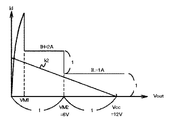
なお、図11のk2は負荷駆動回路20における負荷特性であり、単一の電流制限値ILとした場合の負荷特性k3と比較すると適用可能な負荷条件が拡大している。以上のように、特許文献2で開示された負荷駆動回路20では、出力電圧Voutに応じて電流制限値を2段階に変化させるため負荷条件の拡大が図れる。その結果、特許文献1で開示された負荷駆動回路10では、電流制限値Imが単一に固定されているため低電圧領域では過剰な(必要以上の)電流制限となり、広い負荷条件に適用できない問題点を解決する。
Note that k2 in FIG. 11 is a load characteristic in the
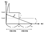
特許文献2で開示されたように、負荷特性を広くするために電流制限特性を2段階とする場合、電源電圧を2等分した電圧ポイントにおいて、最大電流制限値を2等分した電流値だけ変化させると、高・低の両電圧領域において概ね均等な最大制限電力を得ることができる。
As disclosed in
図12は、電源電圧Vcc及び最大電流制限値IHをそれぞれ1:1に均等分割した場合の電流−電圧特性を示す図である。図13は、上述の電源電圧Vccの分割比を1:2、最大電流制限値IHの分割比を2:1にした場合の電流−電圧特性を示す図である。図14は、上述の電源電圧Vccの分割比を2:1、最大電流制限値IHの分割比を1:2にした場合の電流−電圧特性を示す図である。なお、VM1は極めて小さい電圧であるため、VM1以下の領域は考慮せず以下の説明を行なう。 FIG. 12 is a diagram showing current-voltage characteristics when the power supply voltage Vcc and the maximum current limit value IH are each equally divided into 1: 1. FIG. 13 is a diagram showing current-voltage characteristics when the power supply voltage Vcc division ratio is 1: 2 and the maximum current limit value IH is 2: 1. FIG. 14 is a diagram showing current-voltage characteristics when the power supply voltage Vcc division ratio is 2: 1 and the maximum current limit value IH division ratio is 1: 2. Since VM1 is an extremely small voltage, the following description will be given without considering the area below VM1.
図12に示すように、Vcc=12V、VM2=6V、IL=1A、IH=2Aであり、高電圧領域における最大制限電力(最大電圧値×電流制限値)は、12W(12V×1A)となる。一方、低電圧領域における最大制限電力は、12W(6V×2A)となり、高・低の両電圧領域において均等な最大制限電力を得ることができる。 As shown in FIG. 12, Vcc = 12V, VM2 = 6V, IL = 1A, IH = 2A, and the maximum limit power (maximum voltage value × current limit value) in the high voltage region is 12 W (12V × 1A). Become. On the other hand, the maximum limit power in the low voltage region is 12 W (6 V × 2 A), and uniform maximum limit power can be obtained in both the high and low voltage regions.
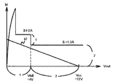
次に、図13に示す分割例では、VM2=4V、IL=1.3A、IH=2Aであり、高電圧領域の最大制限電力は、15.6W(12V×1.3A)、低電圧領域の最大制限電力は、8W(4V×2A)となり、両電圧領域における最大制限電力がアンバランスな状態になっている。 Next, in the division example shown in FIG. 13, VM2 = 4V, IL = 1.3A, IH = 2A, and the maximum limit power in the high voltage region is 15.6 W (12V × 1.3A), the low voltage region The maximum power limit is 8 W (4 V × 2 A), and the maximum power limit in both voltage regions is in an unbalanced state.
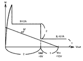
さらに、図14に示す分割例では、VM2=8V、IL=0.7A、IH=2Aであり、高電圧領域の最大制限電力は、8.4W(12V×0.7A)、低電圧領域の最大制限電力は、16W(=8V×2A)となり、やはり両電圧領域における最大制限電力がアンバランスな状態になっている。 Furthermore, in the division example shown in FIG. 14, VM2 = 8V, IL = 0.7A, IH = 2A, and the maximum limit power in the high voltage region is 8.4 W (12V × 0.7A), and in the low voltage region The maximum limit power is 16 W (= 8 V × 2 A), and the maximum limit power in both voltage regions is also in an unbalanced state.
このように、電流制限値を2段階に切り替える場合には、電源電圧を2等分した電圧ポイントにVM2を設定し、最大電流制限値IHを2等分した電流値にILを設定すると、バランスの取れた最大制限電力が得られ、負荷駆動回路全体として負荷特性に適した電流制限を行なうことができる。 Thus, when switching the current limit value in two stages, if VM2 is set to a voltage point obtained by dividing the power supply voltage into two equal parts and IL is set to a current value obtained by dividing the maximum current limit value IH into two equal parts, the balance The maximum power limit can be obtained, and the current limit suitable for the load characteristics can be performed as the entire load driving circuit.
しかし、上述のように、最大制限電力のバランスを考慮して、最大電流制限値IHや切り替え電圧ポイント(VM2)を設定したとしても、当初の設計と異なる電源電圧条件で負荷駆動回路が使用された場合、負荷特性と電流制限特性との適正な関係(バランスが取れた状態)がくずれてしまう。 However, as described above, even if the maximum current limit value IH and the switching voltage point (VM2) are set in consideration of the balance of the maximum limit power, the load drive circuit is used under a power supply voltage condition different from the original design. In this case, an appropriate relationship (a balanced state) between the load characteristic and the current limiting characteristic is lost.
図15を用いてより具体的に説明する。図15は、分割比を1:1と定め設計した負荷駆動回路において、設計時に想定していた電源電圧から変更した場合の電流−電圧特性を示す図である。図15では、Vcc=12V、IL=1A、IH=2A、VM2=6V(分割比1:1)で設計した回路を電源電圧Vcc=10Vの電源で使用する例を示す。 This will be described more specifically with reference to FIG. FIG. 15 is a diagram showing current-voltage characteristics when a load driving circuit designed with a division ratio of 1: 1 is changed from a power supply voltage assumed at the time of design. FIG. 15 shows an example in which a circuit designed with Vcc = 12V, IL = 1A, IH = 2A, VM2 = 6V (division ratio 1: 1) is used as a power supply with a power supply voltage Vcc = 10V.
図15に示すように、電源電圧Vccが変化すると、それに伴って負荷特性が変化する(k2→k4)。その結果、電源電圧Vccに対するVM2の相対的な位置が変化し(分割比1:1→3:2)、負荷特性と電流制限特性との適正な関係がくずれてしまう。すると、高・低の両電圧領域における最大制限電力がアンバランスな状態となり、全体として負荷特性に適した電流制限が行なえない。特許文献2で開示された負荷駆動回路20は、複数の電源電圧条件に対する電流制限特性の追従性に関する配慮はされていないことを意味する。即ち、特許文献2で開示された負荷駆動回路20では、負荷特性と電流制限特性とは互いに独立した関係であるといえる。
As shown in FIG. 15, when the power supply voltage Vcc changes, the load characteristics change accordingly (k2 → k4). As a result, the relative position of VM2 with respect to the power supply voltage Vcc changes (division ratio 1: 1 → 3: 2), and an appropriate relationship between the load characteristic and the current limiting characteristic is lost. Then, the maximum limit power in both the high and low voltage regions is in an unbalanced state, and the current limit suitable for the load characteristics as a whole cannot be performed. The
[第1の実施形態]
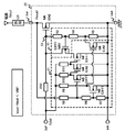
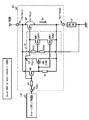
次に、本発明の第1の実施形態について、図面を用いてより詳細に説明する。図16は、第1の実施形態に係る負荷駆動回路30の構成を示す一例である。図16において図3と同一構成要素には、同一の符号を表し、その説明を省略する。
[First Embodiment]
Next, the first embodiment of the present invention will be described in more detail with reference to the drawings. FIG. 16 is an example showing the configuration of the
図3に示す負荷駆動回路10と負荷駆動回路30の相違点は、負荷駆動回路30が電流制限値切り替え回路31を備える点である。電流制限値切り替え回路31は、MOSトランジスタM11及びM12と、抵抗R13及びR14から構成されている。電流制限値切り替え回路31は、出力MOSトランジスタM1と出力端子Out間を導通させ、出力電流Idが流れる経路とは別の電流路として役割を有する。さらに、電源電圧Vcc(電源電圧Vccと接地間の電圧)に応じて2つの異なる電流制限値を切り替える役割を有する。なお、MOSトランジスタM3及びM11の閾値電圧は同じ電圧値とし、スイッチの役目をするMOSトランジスタM12のオン抵抗及び閾値電圧Vt12は無視できるものとする。
The difference between the
また、抵抗R13とR14の抵抗値比は1:1とし、電源電圧Vccの1/2の電圧ポイントで最大電流制限値の1/2だけ制限電流値を変化させる回路となっている。抵抗R13及びR14は、電源端子Pinと接地間に直列接続されている。MOSトランジスタM11のドレインはMOSトランジスタM12のソースに、ソースは出力端子Outに、ゲートはMOSトランジスタM3のゲートと接続されている。MOSトランジスタM12のドレインは出力MOSトランジスタM1のゲートに接続され、ソースはMOSトランジスタM11のドレインに接続され、ゲートは抵抗R13及びR14の接続点に接続されている。なお、出力MOSトランジスタM1のゲートと、MOSトランジスタM3及びM12のドレインの接続点をノードS2とする。 The resistance value ratio of the resistors R13 and R14 is 1: 1, and the limiting current value is changed by 1/2 of the maximum current limiting value at a voltage point of 1/2 of the power supply voltage Vcc. The resistors R13 and R14 are connected in series between the power supply terminal Pin and the ground. The drain of the MOS transistor M11 is connected to the source of the MOS transistor M12, the source is connected to the output terminal Out, and the gate is connected to the gate of the MOS transistor M3. The drain of the MOS transistor M12 is connected to the gate of the output MOS transistor M1, the source is connected to the drain of the MOS transistor M11, and the gate is connected to the connection point of the resistors R13 and R14. A connection point between the gate of the output MOS transistor M1 and the drains of the MOS transistors M3 and M12 is defined as a node S2.
次に、負荷駆動回路30の動作について説明する。負荷駆動回路30では、センス電流Isの増加に伴い抵抗R2の両端電圧が増加してMOSトランジスタM3がオン状態になる。すると、出力MOSトランジスタM1のゲートと出力端子Out間に、オン状態のMOSトランジスタM3を経由する第1の電流路が形成される。その際には、MOSトランジスタM11もオン状態になる。
Next, the operation of the
さらに、MOSトランジスタM11がMOSトランジスタM3と同時にオン状態の場合において、抵抗R13及びR14による電源電圧Vccの分圧電圧と出力電圧Voutとの電圧差が、MOSトランジスタM12の閾値電圧Vt12以上になるとMOSトランジスタM12がオン状態となる。このことによって、前述の第1の電流路と並列にオン状態のMOSトランジスタM11及びM12を経由する第2の電流路が形成される。このように、2つの異なる電流制限値が生成できる。 Further, when the MOS transistor M11 is in the ON state simultaneously with the MOS transistor M3, the MOS transistor M12 has a voltage difference between the divided voltage of the power supply voltage Vcc and the output voltage Vout equal to or higher than the threshold voltage Vt12 of the MOS transistor M12. The transistor M12 is turned on. As a result, a second current path is formed through the MOS transistors M11 and M12 in the on state in parallel with the first current path. In this way, two different current limit values can be generated.
図17乃至図19は、図16に示す各MOSトランジスタのオン/オフ状態を、出力電圧の範囲に応じて併記した図である。図20は、入力電圧と出力電圧の関係を示すタイミングチャートであり、図21は負荷特性と電流制限特性の関係を示す電流−電圧特性図である。なお、各MOSトランジスタのオン抵抗をMOSトランジスタの符号番号を用いて表現し、以下の説明を行なう。例えば、出力MOSトランジスタM1のオン抵抗はrm1と表記する。また、MOSトランジスタM12はスイッチとして動作し、閾値電圧Vt12及びオン抵抗rm12は、無視できるものとする。 17 to 19 are diagrams in which the on / off states of the MOS transistors shown in FIG. 16 are shown in accordance with the output voltage range. FIG. 20 is a timing chart showing the relationship between the input voltage and the output voltage, and FIG. 21 is a current-voltage characteristic diagram showing the relationship between the load characteristic and the current limiting characteristic. Note that the on-resistance of each MOS transistor is expressed using the code number of the MOS transistor, and the following description will be given. For example, the on-resistance of the output MOS transistor M1 is expressed as rm1. The MOS transistor M12 operates as a switch, and the threshold voltage Vt12 and the on-resistance rm12 can be ignored.
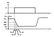
図20に示すように、入力電圧がLレベルの時は、出力MOSトランジスタM1はオフ状態であり、電流は流れない。そのため、出力電圧Voutは接地電圧(0V)となり、Vcc−Vout=Vccとなる。 As shown in FIG. 20, when the input voltage is at the L level, the output MOS transistor M1 is in an off state and no current flows. Therefore, the output voltage Vout becomes the ground voltage (0 V), and Vcc−Vout = Vcc.
次に、時刻t5に入力信号VinがHレベルに遷移すると、出力MOSトランジスタM1は導通を始める。MOSトランジスタM3のゲートには、式(6)で表せる電圧が印加される。
![]()
![]()
一方、MOSトランジスタM12のゲートには、式(7)で表せる電圧が印加される。
![]()
![]()
そのため、出力MOSトランジスタM1のゲートと出力端子Out間には、オン状態のMOSトランジスタM3を経由する第1の電流路と、オン状態のMOSトランジスタM11及びM12を経由する第2の電流路が並列に形成され、MOSトランジスタM1のゲート電圧(ノードS2の電圧)が定まる。この時の電圧をVg2とする。その結果、出力電流Idは電圧Vg2によって定まる電流値I2に制限される。 Therefore, between the gate of the output MOS transistor M1 and the output terminal Out, a first current path passing through the on-state MOS transistor M3 and a second current path passing through the on-state MOS transistors M11 and M12 are parallel. The gate voltage of the MOS transistor M1 (the voltage at the node S2) is determined. The voltage at this time is Vg2. As a result, the output current Id is limited to a current value I2 determined by the voltage Vg2.
ここで、抵抗R13とR14の抵抗値の比は1:1とし、MOSトランジスタM12の閾値電圧Vt12は極めて小さい値のため無視できるものとすると、VN2は略Vccの1/2の電圧値となる。また、ゲート電圧Vg2は式(8)で表すことのできる電圧である。
![]()
![]()
さらに、出力電流Idが増加して電圧(Vcc−Vout)が低下し、VN1≦(Vcc−Vout)<VN2の範囲では、図18(図20のt6<t≦t7の範囲時に相当)に示すように、MOSトランジスタM3及びM11はオン状態、MOSトランジスタM12はオフ状態となる。 Further, the output current Id increases and the voltage (Vcc−Vout) decreases, and in the range of VN1 ≦ (Vcc−Vout) <VN2, it is shown in FIG. 18 (corresponding to the range of t6 <t ≦ t7 in FIG. 20). Thus, the MOS transistors M3 and M11 are turned on, and the MOS transistor M12 is turned off.
これにより、出力MOSトランジスタM1のゲートと出力端子Out間では、第2の電流路は遮断され、オン状態のMOSトランジスタM3を経由する第1の電流路のみが導通し、出力MOSトランジスタM1のゲート電圧が定まる。この時の電圧をVg1とする。その結果、出力電流Idはゲート電圧Vg1で決定される電流値I1に制限される。なお、ゲート電圧Vg1は式(9)により表せる電圧である。
![]()
![]()
さらに、出力電流Idが増加することで電圧(Vcc−Vout)が低下し、(Vcc−Vout)<VN1の範囲内では、図19(図20のt7<t≦t8の範囲時に相当)に示すように、MOSトランジスタM3、M11及びM12が全てオフ状態になる。そして、出力MOSトランジスタM1のゲートには、入力電圧Vinが印加され、負荷LDの抵抗値rLと出力MOSトランジスタM1の内部抵抗値rm1で決まる動作点B(Vb、Ib)に遷移する。 Further, as the output current Id increases, the voltage (Vcc−Vout) decreases. As shown in FIG. 19 (corresponding to the range of t7 <t ≦ t8 in FIG. 20) within the range of (Vcc−Vout) <VN1. Thus, the MOS transistors M3, M11, and M12 are all turned off. Then, the input voltage Vin is applied to the gate of the output MOS transistor M1, and a transition is made to an operating point B (Vb, Ib) determined by the resistance value rL of the load LD and the internal resistance value rm1 of the output MOS transistor M1.
その後、負荷LDが短絡すると、電圧(Vcc−Vout)は、略電源電圧Vccに等しくなり、MOSトランジスタM3、M11及びM12が全てオン状態となることで、出力MOSトランジスタM1のゲート電圧をVg2にバイアスする。このように、負荷短絡時には出力MOSトランジスタM1に流れる出力電流Idを電流制限値I2に制限して出力MOSトランジスタM1を熱破壊から保護する。 Thereafter, when the load LD is short-circuited, the voltage (Vcc−Vout) becomes substantially equal to the power supply voltage Vcc, and the MOS transistors M3, M11, and M12 are all turned on, so that the gate voltage of the output MOS transistor M1 is set to Vg2. Bias. In this way, when the load is short-circuited, the output current Id flowing through the output MOS transistor M1 is limited to the current limit value I2 to protect the output MOS transistor M1 from thermal destruction.
負荷駆動回路30の電流−電圧特性の一例を図21及び図22に示す。図21はI1=2A、I2=1A(最大電流制限値の分割比1:1)、VN2=6V(電源電圧の分割比1:1)に設定し、電源電圧を12Vで使用した場合の電流−電圧特性図である。図22は、図21の条件から電源電圧を10Vに変更した場合の電流−電圧特性図である。
An example of the current-voltage characteristic of the
図21に示すように、12V電源で使用した場合には、(Vcc−Vout)≧VN2(6V)の高電圧領域では、出力電流Idは制限電流I2(1A)に制限される。一方、(Vcc−Vout)<VN2の低電圧領域では、出力電流Idは制限電流I1(2A)に制限される。従って、高電圧領域における最大制限電力は、12W(12V×1A)となる。一方、低電圧領域における最大制限電力は、12W(6V×2A)となり、高・低の両電圧領域において均等な最大制限電力が得られる。 As shown in FIG. 21, when used with a 12V power supply, the output current Id is limited to the limiting current I2 (1A) in the high voltage region of (Vcc−Vout) ≧ VN2 (6V). On the other hand, in the low voltage region where (Vcc−Vout) <VN2, the output current Id is limited to the limiting current I1 (2A). Therefore, the maximum limit power in the high voltage region is 12 W (12 V × 1 A). On the other hand, the maximum limit power in the low voltage region is 12 W (6 V × 2 A), and uniform maximum limit power is obtained in both the high and low voltage regions.
次に、負荷駆動回路30を電源電圧10Vで使用した場合、負荷特性がk2からk5に変化する。このような場合、負荷駆動回路20では負荷特性と電流制限特性の適正な関係がくずれ、VccのVM2による分割比が変化して、高・低の両電圧領域における最大制限電力がアンバランスな状態となる。しかし、負荷駆動回路30では、図22に示すように、Vccの変化に追従して、VccのVN2による分割比を一定に保持しつつVN2が変化する。例えば、図22の例では、VN2の電圧が6Vから5Vに変化している。
Next, when the
このため、高電圧領域における最大制限電力は、10W(=10V×1A)、低電圧領域における最大制限電力は、10W(=5V×2A)となり、高・低の両電圧領域において均等な最大制限電力を得ることができる。 For this reason, the maximum power limit in the high voltage region is 10 W (= 10 V × 1 A), and the maximum power limit in the low voltage region is 10 W (= 5 V × 2 A). Electric power can be obtained.
なお、本実施形態の説明では、抵抗R13及びR14の抵抗値比を1:1に設定して、Vccの1/2の電圧ポイントで電流制限値を変化させる場合を説明したが、この抵抗値比を適宜、設定することで、任意の電圧ポイントで電流制限値を切り替えることができる。さらに、本実施形態の説明では、2段階に電流制限値を可変する回路構成で説明したが、2以上の分圧電圧を生成する分圧回路とスイッチMOSトランジスタをさらに設けて、切り替え回路を増設することで、電源電圧に応じて複数の切り替え電圧ポイントが可変する複数段階の電流制限が可能となる。 In the description of the present embodiment, the case where the resistance value ratio of the resistors R13 and R14 is set to 1: 1 and the current limit value is changed at a voltage point of 1/2 of Vcc has been described. By setting the ratio appropriately, the current limit value can be switched at an arbitrary voltage point. Furthermore, in the description of the present embodiment, the circuit configuration has been described in which the current limit value is variable in two stages. However, a voltage dividing circuit that generates two or more divided voltages and a switch MOS transistor are further provided to increase the switching circuit. By doing so, it is possible to limit the current in a plurality of stages in which a plurality of switching voltage points vary according to the power supply voltage.
以上のように、負荷駆動回路30では、異なる2つの電流制限値を切り替えて段階的な電流制限を可能にしている。そのため、低電圧領域で過剰な電流制限とならず、負荷条件の範囲が拡大している。同時に、電流制限値の切り替え電圧ポイントは、電源電圧に応じて、電源電圧の分割比を保持しつつ変化するため、異なる電源電圧条件で使用しても電流制限特性が追従して変化し、全体として負荷特性に適した電流制限が行なえる。さらに、2段階に電流制限を行なう場合、電源電圧の1/2の電圧ポイントにおいて、最大電流制限値の1/2だけ制限電流値を変化させるようにすると、高・低の両電圧領域で均等な最大制限電力を得ることができる。また、電流制限値の切り替え電圧ポイントは、分圧抵抗の抵抗値比を変更することによって任意の電圧に設定できる。
As described above, in the
なお、上記の特許文献等の各開示を、本書に引用をもって繰り込むものとする。本発明の全開示(請求の範囲を含む)の枠内において、さらにその基本的技術思想に基づいて、実施形態の変更・調整が可能である。また、本発明の請求の範囲の枠内において種々の開示要素の多様な組み合わせないし選択が可能である。すなわち、本発明は、請求の範囲を含む全開示、技術的思想にしたがって当業者であればなし得るであろう各種変形、修正を含むことは勿論である。例えば、実施形態の説明においては、正電源を使用することを想定して、nチャンネル型MOSトランジスタを使用したが、負電源を使用する場合には、pチャンネル型MOSトランジスタを用いることができる。 It should be noted that the disclosures of the above patent documents and the like are incorporated herein by reference. Within the scope of the entire disclosure (including claims) of the present invention, the embodiment can be changed and adjusted based on the basic technical concept. Various combinations and selections of various disclosed elements are possible within the scope of the claims of the present invention. That is, the present invention of course includes various variations and modifications that could be made by those skilled in the art according to the entire disclosure including the claims and the technical idea. For example, in the description of the embodiment, an n-channel MOS transistor is used on the assumption that a positive power supply is used. However, when a negative power supply is used, a p-channel MOS transistor can be used.
10、20、30 負荷駆動回路
21 電圧検出回路
22 電圧クランプ回路
31 電流制限値切り替え回路
LD 負荷
M1〜M12 MOSトランジスタ
R1〜R14 抵抗
CP チャージポンプ回路
10, 20, 30
Claims (6)
前記出力MOSトランジスタの出力電圧に応じて、前記出力MOSトランジスタに流れる出力電流を複数段階の制限電流に制限すると共に、前記制限電流が切り替わる際の出力電圧を電源電圧の変化に基づいて切り替える電流制限値切り替え回路と、
を備えることを特徴とする負荷駆動回路。 An output MOS transistor connected to a power source and a load;
Current limiting that limits the output current flowing through the output MOS transistor to a plurality of stages of limiting current according to the output voltage of the output MOS transistor and that switches the output voltage when the limiting current is switched based on a change in power supply voltage A value switching circuit;
A load driving circuit comprising:
前記電流検出用MOSトランジスタに流れる電流に基づいて、前記出力MOSトランジスタのゲート電圧を変動させる第1のMOSトランジスタと、
を備える請求項1又は2の負荷駆動回路。 Furthermore, a current detection MOS transistor for measuring an output current flowing through the output MOS transistor;
A first MOS transistor that varies a gate voltage of the output MOS transistor based on a current flowing through the current detection MOS transistor;
A load driving circuit according to claim 1 or 2.
電源電圧から分圧電圧を生成する第1の抵抗及び第2の抵抗と、
前記分圧電圧と出力電圧の電圧差に基づいて、前記出力MOSトランジスタのゲート電圧を変動させる第2のMOSトランジスタと、
を備え、
前記第1のMOSトランジスタは、前記第2のMOSトランジスタに対応して導通する請求項3の負荷駆動回路。 The current limit value switching circuit is:
A first resistor and a second resistor for generating a divided voltage from the power supply voltage;
A second MOS transistor that varies a gate voltage of the output MOS transistor based on a voltage difference between the divided voltage and the output voltage;
With
4. The load driving circuit according to claim 3, wherein the first MOS transistor conducts in correspondence with the second MOS transistor.
Priority Applications (1)
| Application Number | Priority Date | Filing Date | Title |
|---|---|---|---|
| JP2011019425A JP2012160928A (en) | 2011-02-01 | 2011-02-01 | Load drive circuit |
Applications Claiming Priority (1)
| Application Number | Priority Date | Filing Date | Title |
|---|---|---|---|
| JP2011019425A JP2012160928A (en) | 2011-02-01 | 2011-02-01 | Load drive circuit |
Publications (1)
| Publication Number | Publication Date |
|---|---|
| JP2012160928A true JP2012160928A (en) | 2012-08-23 |
Family
ID=46841101
Family Applications (1)
| Application Number | Title | Priority Date | Filing Date |
|---|---|---|---|
| JP2011019425A Withdrawn JP2012160928A (en) | 2011-02-01 | 2011-02-01 | Load drive circuit |
Country Status (1)
| Country | Link |
|---|---|
| JP (1) | JP2012160928A (en) |
Cited By (3)
| Publication number | Priority date | Publication date | Assignee | Title |
|---|---|---|---|---|
| JP2014128005A (en) * | 2012-12-27 | 2014-07-07 | Renesas Electronics Corp | Semiconductor device and electronic control apparatus |
| CN104756381A (en) * | 2012-11-08 | 2015-07-01 | 大金工业株式会社 | Power converter |
| JP7434344B2 (en) | 2021-07-20 | 2024-02-20 | ティーシーエル チャイナスター オプトエレクトロニクス テクノロジー カンパニー リミテッド | current limit circuit |
-
2011
- 2011-02-01 JP JP2011019425A patent/JP2012160928A/en not_active Withdrawn
Cited By (3)
| Publication number | Priority date | Publication date | Assignee | Title |
|---|---|---|---|---|
| CN104756381A (en) * | 2012-11-08 | 2015-07-01 | 大金工业株式会社 | Power converter |
| JP2014128005A (en) * | 2012-12-27 | 2014-07-07 | Renesas Electronics Corp | Semiconductor device and electronic control apparatus |
| JP7434344B2 (en) | 2021-07-20 | 2024-02-20 | ティーシーエル チャイナスター オプトエレクトロニクス テクノロジー カンパニー リミテッド | current limit circuit |
Similar Documents
| Publication | Publication Date | Title |
|---|---|---|
| KR102380611B1 (en) | Current sensing and control for transistor power switches | |
| JP4921106B2 (en) | Buffer circuit | |
| US8665020B2 (en) | Differential amplifier circuit that can change current flowing through a constant-current source according to load variation, and series regulator including the same | |
| KR101411812B1 (en) | Voltage regulator | |
| CN109039328B (en) | Driver circuit with gate clamp supporting stress test | |
| US7359171B2 (en) | Current limiting circuit and output circuit including the same | |
| WO2016009582A1 (en) | Voltage controlled device drive circuit | |
| JP2007096731A (en) | Mute circuit | |
| US20110133813A1 (en) | Analog switch with a low flatness operating characteristic | |
| CN106066419B (en) | Current detection circuit | |
| JP2012160928A (en) | Load drive circuit | |
| JP2006112906A (en) | Voltage detection circuit | |
| WO2008085781A1 (en) | Biasing current to speed up current mirror settling time | |
| US9798346B2 (en) | Voltage reference circuit with reduced current consumption | |
| US7116537B2 (en) | Surge current prevention circuit and DC power supply | |
| US8773168B2 (en) | Maximum voltage selection circuit and method and sub-selection circuit | |
| US10094857B2 (en) | Current detection circuit | |
| CN106571797B (en) | Power-on reset (POR) circuit | |
| EP1091485A1 (en) | Input stage for buffer with negative feedback | |
| JP3855810B2 (en) | Differential amplifier circuit | |
| JP4384008B2 (en) | Level shift circuit | |
| US5719524A (en) | Circuit having an input terminal for controlling two functions | |
| US9836073B2 (en) | Current source, an integrated circuit and a method | |
| US9281746B1 (en) | System and method for a diagnostic circuit | |
| JP2018061115A (en) | Enable signal generation circuit |
Legal Events
| Date | Code | Title | Description |
|---|---|---|---|
| A300 | Withdrawal of application because of no request for examination |
Free format text: JAPANESE INTERMEDIATE CODE: A300 Effective date: 20140401 |