JP2012155131A - Developing device and image forming apparatus - Google Patents
Developing device and image forming apparatus Download PDFInfo
- Publication number
- JP2012155131A JP2012155131A JP2011013965A JP2011013965A JP2012155131A JP 2012155131 A JP2012155131 A JP 2012155131A JP 2011013965 A JP2011013965 A JP 2011013965A JP 2011013965 A JP2011013965 A JP 2011013965A JP 2012155131 A JP2012155131 A JP 2012155131A
- Authority
- JP
- Japan
- Prior art keywords
- developer
- toner
- bias
- developing
- carrier
- Prior art date
- Legal status (The legal status is an assumption and is not a legal conclusion. Google has not performed a legal analysis and makes no representation as to the accuracy of the status listed.)
- Pending
Links
Images


Classifications
-
- G—PHYSICS
- G03—PHOTOGRAPHY; CINEMATOGRAPHY; ANALOGOUS TECHNIQUES USING WAVES OTHER THAN OPTICAL WAVES; ELECTROGRAPHY; HOLOGRAPHY
- G03G—ELECTROGRAPHY; ELECTROPHOTOGRAPHY; MAGNETOGRAPHY
- G03G15/00—Apparatus for electrographic processes using a charge pattern
- G03G15/06—Apparatus for electrographic processes using a charge pattern for developing
- G03G15/08—Apparatus for electrographic processes using a charge pattern for developing using a solid developer, e.g. powder developer
- G03G15/0806—Apparatus for electrographic processes using a charge pattern for developing using a solid developer, e.g. powder developer on a donor element, e.g. belt, roller
- G03G15/0813—Apparatus for electrographic processes using a charge pattern for developing using a solid developer, e.g. powder developer on a donor element, e.g. belt, roller characterised by means in the developing zone having an interaction with the image carrying member, e.g. distance holders
-
- G—PHYSICS
- G03—PHOTOGRAPHY; CINEMATOGRAPHY; ANALOGOUS TECHNIQUES USING WAVES OTHER THAN OPTICAL WAVES; ELECTROGRAPHY; HOLOGRAPHY
- G03G—ELECTROGRAPHY; ELECTROPHOTOGRAPHY; MAGNETOGRAPHY
- G03G2215/00—Apparatus for electrophotographic processes
- G03G2215/01—Apparatus for electrophotographic processes for producing multicoloured copies
- G03G2215/0103—Plural electrographic recording members
- G03G2215/0119—Linear arrangement adjacent plural transfer points
- G03G2215/0122—Linear arrangement adjacent plural transfer points primary transfer to an intermediate transfer belt
- G03G2215/0125—Linear arrangement adjacent plural transfer points primary transfer to an intermediate transfer belt the linear arrangement being horizontal or slanted
- G03G2215/0129—Linear arrangement adjacent plural transfer points primary transfer to an intermediate transfer belt the linear arrangement being horizontal or slanted horizontal medium transport path at the secondary transfer
Abstract
Description
本発明は、電子写真方式を利用した複写機やプリンタ等の画像形成装置及びこれに用いられる現像装置に関するものである。 The present invention relates to an image forming apparatus such as a copying machine or a printer using an electrophotographic system, and a developing device used therefor.
従来の電子写真方式の画像形成装置では、帯電したトナーを像担持体に接近させ、静電的にトナーを像担持体上の静電潜像に付着させることにより現像が行なわれ、画像が形成される。現像剤としては、非磁性トナーと磁性キャリアとを主成分とする二成分現像剤が広く用いられている。 In a conventional electrophotographic image forming apparatus, a charged toner is brought close to an image carrier, and development is performed by electrostatically attaching the toner to an electrostatic latent image on the image carrier to form an image. Is done. As the developer, a two-component developer mainly composed of a non-magnetic toner and a magnetic carrier is widely used.
現像剤を像担持体へと移動させる現像バイアスとしては、直流電圧に交流電圧を重畳させるAC現像と直流電圧のみを利用するDC現像とがある。AC現像は画質面において優れているのに対し、DC現像は簡易な構成や低コストがその長所である。 The development bias for moving the developer to the image carrier includes AC development in which an AC voltage is superimposed on a DC voltage and DC development using only a DC voltage. While AC development is superior in terms of image quality, DC development is advantageous in that it has a simple configuration and low cost.
二成分現像剤を用いた二成分AC現像方式では、例えば、200V程度の直流電圧にVp−p=2kV程度の矩形波の交流電圧を重畳したバイアスが用いられる。現像バイアスの直流成分は、現像剤担持体表面上の現像剤中のトナーを像担持体へと向かわせる為に印加されるのに対し、交流成分には、瞬間的に大きな電界をかけることによって現像剤中で互いに逆極性に帯電しているトナーとキャリアを分離させる効果がある。 In the two-component AC development method using a two-component developer, for example, a bias in which a rectangular wave AC voltage of about V p−p = 2 kV is superimposed on a DC voltage of about 200 V is used. The DC component of the developing bias is applied to direct the toner in the developer on the surface of the developer carrier to the image carrier, whereas the AC component is instantaneously applied with a large electric field. There is an effect of separating the toner and the carrier charged in opposite polarities in the developer.
一方、二成分現像剤を用いた二成分DC現像方式では直流電圧のみによって現像が行なわれる。この直流電圧の大きさはAC現像に於ける交流電圧と比較して小さい為、現像バイアスによるトナーとキャリアの分離作用は小さい。このため、現像バイアスの下で動くことのできるトナー粒子の数は少なく、必然的に像担持体に現像されるトナーの量も少なくなるので画像濃度が出にくい。 On the other hand, in the two-component DC development method using a two-component developer, development is performed only by a direct current voltage. Since the magnitude of the DC voltage is smaller than the AC voltage in AC development, the toner and carrier separation action by the developing bias is small. For this reason, the number of toner particles that can move under the developing bias is small, and the amount of toner developed on the image carrier is inevitably small, so that the image density is hardly generated.
画像濃度を向上させる方法としては、現像剤中のトナー濃度を上げたり、現像剤担持体の現像剤搬送速度を上げる、現像バイアスを大きくする方法等がある。しかし、現像剤中のトナー濃度を上げると、像担持体上の非画像領域にトナーが付着する、という所謂かぶりが起きやすくなる。また、現像剤搬送速度を上げると、現像剤の劣化が加速されることが知られている。 As a method for improving the image density, there are a method for increasing the toner density in the developer, a method for increasing the developer conveying speed of the developer carrier, and a method for increasing the developing bias. However, when the toner concentration in the developer is increased, the so-called fogging that the toner adheres to the non-image area on the image carrier tends to occur. Further, it is known that when the developer conveyance speed is increased, the deterioration of the developer is accelerated.
また、現像バイアスを大きくすると、トナーに働く力が大きくなるので、トナーとキャリアの分離性を上げることができ、画像濃度を上昇させることができる。しかし、像担持体上の画像領域にキャリアが付着する確率も飛躍的に大きくなるため、現像バイアス大きくすることで画像濃度を上げることには限界がある。 Further, when the developing bias is increased, the force acting on the toner increases, so that the separation property between the toner and the carrier can be increased, and the image density can be increased. However, since the probability that the carrier adheres to the image area on the image carrier increases dramatically, there is a limit to increasing the image density by increasing the developing bias.
そこで、特許文献1(特開平4−70874)では、現像領域の直前に二成分現像剤中のトナーを引き付ける励起電極を設置している。これにより、現像剤が励起電極位置を通過して現像領域に至るとき、現像剤中のトナーを励起電極側により引き付け、感光体と接触する現像剤のトナー濃度を高めている。 Therefore, in Patent Document 1 (Japanese Patent Laid-Open No. 4-70874), an excitation electrode that attracts toner in the two-component developer is provided immediately before the development region. As a result, when the developer passes through the excitation electrode position and reaches the development region, the toner in the developer is attracted by the excitation electrode side, and the toner concentration of the developer in contact with the photoreceptor is increased.
しかし、特許文献1に記載の技術では、現像剤中のトナーを動かす力は依然として弱く、電極の効果は薄い。
However, in the technique described in
そこで本発明は、現像領域の現像剤搬送方向上流側の電極部材と現像剤担持体との間に現像電界よりも大きな電界が形成されるように電圧を印加する。これによって、現像剤表面のトナー濃度を高め、よりいっそう画像濃度を高めることができる現像装置及び画像形成装置を提供することを目的とする。 Therefore, in the present invention, a voltage is applied so that an electric field larger than the developing electric field is formed between the electrode member on the upstream side in the developer conveying direction of the developing region and the developer carrying member. Accordingly, an object of the present invention is to provide a developing device and an image forming apparatus that can increase the toner density on the developer surface and further increase the image density.
上記課題を解決するために本発明に係る現像装置及び画像形成装置の代表的な構成は、静電潜像を担持する像担持体に対向して配置され、トナーとキャリアを有する現像剤を現像領域まで搬送する現像剤担持体と、前記現像領域よりも現像剤搬送方向上流側に配置された電極部材と、を有し、前記電極部材と前記像担持体の間にプレバイアスをかけ、前記現像剤担持体に直流電圧を印加し、前記現像剤担持体と前記像担持体の間に現像バイアスをかけて、前記現像剤担持体上の現像剤中のトナーを前記像担持体へ移動させて、前記像担持体上の静電潜像を現像する現像装置において、前記プレバイアスによる前記電極部材と前記現像剤担持体との間の電界強度が、前記現像バイアスによる前記像担持体と前記現像剤担持体との間の電界強度よりも大きいことを特徴とする。 In order to solve the above problems, a typical configuration of a developing device and an image forming apparatus according to the present invention is arranged to face an image carrier that carries an electrostatic latent image, and develops a developer having toner and a carrier. A developer carrier that transports to the region, and an electrode member that is disposed upstream of the development region in the developer transport direction, and applies a pre-bias between the electrode member and the image carrier, A DC voltage is applied to the developer carrier, a developing bias is applied between the developer carrier and the image carrier, and the toner in the developer on the developer carrier is moved to the image carrier. In the developing device for developing the electrostatic latent image on the image carrier, the electric field strength between the electrode member and the developer carrier by the pre-bias is such that the image carrier and the developer by the development bias are The electric field strength between the developer carrier Characterized in that also large.
本発明によれば、現像領域の現像剤搬送方向上流側の電極部材と現像剤担持体との間に現像電界よりも大きな電界が形成されるように電圧を印加することによって、現像剤表面のトナー濃度を高め、よりいっそう画像濃度を高めることができる。 According to the present invention, by applying a voltage so that an electric field larger than the developing electric field is formed between the electrode member on the upstream side in the developer conveying direction of the developing region and the developer carrying member, The toner density can be increased and the image density can be further increased.
[第1実施形態]
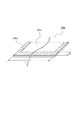
本発明に係る現像装置及び画像形成装置の第1実施形態について、図を用いて説明する。図1は本実施形態に係る画像形成装置100の構成図である。図1に示すように、本実施形態の画像形成装置100は、4個の画像形成部Pa、Pb、Pc、Pdを有している。画像形成部Pa〜Pdは、ほぼ同様の構成をもつため、画像形成部Paを例にとって画像形成部を説明する。
[First embodiment]
A developing device and an image forming apparatus according to a first embodiment of the invention will be described with reference to the drawings. FIG. 1 is a configuration diagram of an
画像形成部Paにおいて、原稿のイエロー成分色による画像信号に応じてレーザースキャナー11aからレーザー光が発射され、1次帯電器22aによって帯電された感光ドラム1a上(像担持体上)に静電潜像が形成される。この静電潜像は、現像装置23aによりイエロートナー像として現像される。イエロートナー像は、1次転写ローラ26aと感光ドラム(像担持体)1aにより挟持された中間転写ベルト81が感光ドラム1aと当接する1次転写ニップ部T1aにて中間転写ベルト81に1次転写される。1次転写後に感光ドラムに残留したトナーは、クリーニング器12によって除去される。イエロートナー像を担持した中間転写ベルト81は、画像形成部Pb〜Pdにて同様に形成されたマゼンタ、シアン、ブラックのトナー像を重畳転写される。
In the image forming section Pa, a laser beam is emitted from the
一方、給送カセット60に積載されたシート(記録媒体)Pは、ピックアップローラ61、搬送ローラ62により、2次転写内ローラ(転写手段)29と2次転写外ローラ40とが当接する2次転写部T2に搬送され、4色のトナー像を2次転写される。2次転写されたトナー像は、定着装置91により加熱加圧されて、シートPに定着し、画像形成装置本体外へ排出される。
On the other hand, the sheet (recording medium) P loaded on the
図2に示すように、本実施形態の現像装置23aは、マイナス帯電の非磁性トナーと磁性キャリアとを主成分とする二成分現像剤を用いている。現像装置23aの内部は、現像位置において垂直方向に延在する隔壁によって、第1室(現像室)と第2室(攪拌室)とに区画されている。第1室には、非磁性の現像スリーブ(現像剤担持体)231aが配置されており、現像スリーブ231a内には磁界発生手段としてのマグネットが固定配置されている。
As shown in FIG. 2, the developing
第1室、第2室にはそれぞれ、第1、第2のスクリュー232a、233aが配置されている。第1のスクリュー232aは、第1室中の現像剤を攪拌搬送する。第2のスクリュー233aは、トナー補給槽30aから供給されたトナーと、現像装置23a内にある現像剤とを攪拌搬送し、現像剤のトナー濃度を均一にする。第1室と第2室との間の隔壁には、手前側と奥側の端部において第1室と第2室とを相互に連通させる現像剤通路が形成されている。第1、第2スクリュー232a、233aの搬送力により、現像によってトナーが消費されて現像剤のトナー濃度が低下した第1室内の現像剤が一方の通路から第2室へ移動する。第2室内で現像剤のトナー濃度の回復した現像剤が他方の通路から第1室内へ移動する。
First and
現像装置23a内の二成分現像剤は、マグネットの磁力により現像スリーブ231a上(現像剤担持体上)に担持される。次いで、現像スリーブ231a上の現像剤は、ブレード234aにより層厚を規制され、現像スリーブ231aの回転に伴って感光ドラム1aと対向した現像領域に搬送される。現像領域において二成分現像剤が磁気ブラシを形成するようにマグネットの磁極は配置されており、磁気ブラシを感光ドラム1aと接触させることによりトナーが静電潜像に供給され、現像が行なわれる。現像効率、すなわち、潜像へのトナー付与率を向上させるために、現像スリーブ221aには現像バイアス出力手段としての現像バイアス電源(不図示)から所定の現像バイアスが印加される。本実施形態では、現像スリーブ231aには、現像バイアス電源から、−500Vの直流電圧が印加される。
The two-component developer in the developing
(補助電極)
図2に示すように、感光ドラム1aと現像スリーブ231aとが対向する現像領域より現像剤搬送方向上流側に補助電極235aを配置している。補助電極235aは現像装置23aに取り付けられている。
(Auxiliary electrode)
As shown in FIG. 2, an
図3は補助電極235aの構成図である。図3に示すように、補助電極235aは、電極部(電極部材)236a、電極支持部材237aを有している。電極部236aは電圧印加可能な金属箔からなる。電極支持部材237aは絶縁性の樹脂からなる。電極部236aは、接着剤等によって電極支持部材237a上に固定されている。
FIG. 3 is a configuration diagram of the
電極部236aの長さlは、現像スリーブ231aの長手方向において、現像スリーブ231aの現像剤担持領域よりも広くなっている。これにより、電極部236aに電圧を印加したとき、現像スリーブ231aの長手方向において、現像スリーブ231a上の現像剤が担持されている領域全域に渡って均一な電界が形成される。電極部236aの幅dは、後述するプレバイアス印加範囲と等しくなるようにする。
The length l of the
電極部236aと現像スリーブ231aとの間に直流電圧(以下、プレバイアスという)を印加し、現像スリーブ231aに対する電極部236aの電位が現像剤中のトナーの電荷と逆極性になるようにする。これにより、図4に示すように、現像剤が補助電極235aを通過するとき、プレバイアスによって形成される電界の作用で、現像剤中のトナーが現像スリーブ側から補助電極側へと引っ張られる。これにより、補助電極側の現像剤のトナー濃度が現像スリーブ側の現像剤のトナー濃度よりも高くなる。そして、感光ドラム1aにはトナー濃度の高い現像剤が触れることになり、補助電極235aが無い構成よりも現像されるトナー像の画像濃度が上昇する。
A DC voltage (hereinafter referred to as pre-bias) is applied between the
(プレバイアス印加範囲)
次に、プレバイアス印加範囲について説明する。特許第3087541号にも記載されているように、プレバイアスを印加しても補助電極と現像スリーブ内のマグネットの磁極の位置によっては高効率の現像が実現できないことがある。
(Pre-bias application range)
Next, the pre-bias application range will be described. As described in Japanese Patent No. 3087541, even when a pre-bias is applied, high-efficiency development may not be realized depending on the positions of the auxiliary electrode and the magnetic pole of the magnet in the developing sleeve.
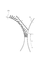
図5は補助電極235aの電圧印加範囲を示す図である。図5に示すように、現像領域Aより最も現像剤搬送方向上流側の領域aにプレバイアスを印加した場合、トナー濃度が高まった磁気穂先端の現像剤は次の磁極位置で反転する。このため、トナー濃度の低い現像剤が現像領域Aにおいて感光ドラム1aと接触することになるので現像性はかえって低下してしまう。
FIG. 5 is a diagram showing a voltage application range of the
次に、領域aの現像剤搬送方向下流側の領域bにプレバイアスを印加した場合、磁気穂先端の現像剤が反転するため、磁気穂が寝ており、磁気穂の側面にトナーが集まることになる。このため、磁気穂先端のトナーが減ってしまうので、やはり現像性は低下してしまう。 Next, when a pre-bias is applied to the region b on the downstream side in the developer transport direction of the region a, the developer at the tip of the magnetic head is inverted, so that the magnetic ear is sleeping and toner is collected on the side surface of the magnetic ear. become. For this reason, since the toner at the tip of the magnetic head is reduced, developability is also lowered.
最後に、領域bの現像剤搬送方向下流側の領域cにプレバイアスを印加した場合、トナーは磁気穂の先端に引き寄せられ、磁気穂先端のトナー濃度が高まった状態で現像が行なわれる。このため、現像性は向上する。 Finally, when a pre-bias is applied to the region c downstream of the developer conveyance direction in the region b, the toner is attracted to the tip of the magnetic spike, and development is performed in a state where the toner concentration at the tip of the magnetic spike is increased. For this reason, developability improves.
以上より、現像領域Aより現像剤搬送方向上流側に位置している現像剤担持体の内側の複数の磁極のうち最も現像領域Aに近い現像主極に対向した磁気穂が立ち上がり始める位置(領域cの位置)に、プレバイアスを印加することが効果的である。 From the above, the position (area) where the magnetic spikes facing the development main pole closest to the development area A among the plurality of magnetic poles inside the developer carrying member located upstream of the development area A in the developer transport direction start (area). It is effective to apply a pre-bias at the position c).
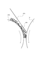
プレバイアスの効果がより発揮される範囲を明確にするために次のような考察を行なった。図6はトナーに作用する力を説明する図である。図6(a)に示すように、現像剤搬送方向(矢印Y方向)を含む平面内において、現像スリーブ231a表面外向き法線Hと磁気穂Gとのなす角度をαとする。このとき、現像スリーブ231a表面外向き法線Hに対して現像剤搬送方向に磁気穂Gが傾く方向をαの正方向とする。
In order to clarify the range in which the effect of the pre-bias is exerted more, the following consideration was made. FIG. 6 is a diagram for explaining the force acting on the toner. As shown in FIG. 6A, the angle formed between the normal H on the surface of the developing
現像スリーブ231aと補助電極235aとが対向する位置において、平行平板近似が成り立ち、補助電極235aに垂直な電界が形成されるとする。図6(a)に示すように、磁気穂Gの角度がαであるとき、図6(b)に示すように、磁気穂中のトナー粒子がこの電界によって受ける力Fは、トナー粒子を磁気穂先端に向かって引っ張る力f1とトナー粒子を磁気穂の側面に寄せる力f2とに分解できる。
It is assumed that a parallel plate approximation is established at a position where the developing
−45°<α<45°の範囲にあるとき、トナーを磁気穂先端に向かって引っ張る力がトナーを磁気穂側面に寄せる力を上回るので、現像剤中のトナーは磁気穂Gの先端に集める力が働き、プレバイアスの効果が発揮される。 When in the range of −45 ° <α <45 °, the force pulling the toner toward the tip of the magnetic spike exceeds the force pulling the toner toward the side of the magnetic spike, so that the toner in the developer is collected at the tip of the magnetic spike G. Power works and the effect of pre-bias is demonstrated.
また、磁気穂Gの形状は、現像スリーブ231aの周りに生じる磁束密度のパターンにほぼ追従するので、α≒tan−1(Bθ/Br)である。ここで、Brは磁束密度の現像スリーブ表面法線方向成分でありる。Bθは磁束密度の現像剤搬送方向成分である。
Further, since the shape of the magnetic spike G substantially follows the pattern of magnetic flux density generated around the developing
図7は磁気穂Gのなす角度αと磁束密度Bθ、Brの関係を示す図である。図7において、現像剤搬送方向において、現像主極に近づくにつれてαが負の値から0に近づく。従って、現像主極近傍でα=−45°、つまり、Bθ/Br=−1となる点(Brと−Bθの二つの曲線の交点)の位置をプレバイアス印加開始点とする。本実施形態の場合、現像主極のピーク位置がα=−8°であるので、プレバイアス印加開始点を−21°にとればよい。 FIG. 7 is a diagram showing the relationship between the angle α formed by the magnetic spike G and the magnetic flux densities B θ and B r . In FIG. 7, in the developer transport direction, α approaches 0 from a negative value as it approaches the main development pole. Therefore, the position of the point where α = −45 °, that is, B θ / B r = −1 (intersection of the two curves of B r and −B θ ) in the vicinity of the developing main pole is set as the pre-bias application start point. . In the present embodiment, since the peak position of the development main electrode is α = −8 °, the pre-bias application start point may be set to −21 °.
プレバイアス印加終了点に関しては次のように決める。バイアスによるトナー引き付け効果はバイアス印加範囲とともに増加する一方で、現像による感光ドラム上のトナー載り量は磁気ブラシ(磁気穂G)と感光ドラム1aの接触距離とともに増加する。このため、バイアス印加開始点からバイアス印加範囲を伸ばしていくと、磁気ブラシと感光ドラム1aとが接触し始める点までは感光ドラム上のトナー載り量は増加する。しかし、電極が現像領域Aに侵入し、磁気ブラシと感光ドラム1aとの接触範囲が狭くなり始めると、感光ドラム上のトナー載り量はかえって減少する。よって、感光ドラム上のトナー載り量の最大値を得られるよう、磁気ブラシと感光ドラム1aとの接触開始点をバイアス印加終了点とした。
The pre-bias application end point is determined as follows. While the toner attracting effect due to the bias increases with the bias application range, the toner applied amount on the photosensitive drum due to the development increases with the contact distance between the magnetic brush (magnetic ear G) and the
プレバイアス印加開始点とプレバイアス印加終了点との間の領域をプレバイアス印加範囲とし、電極部236aの幅dをこのプレバイアス印加範囲と一致させる。
A region between the pre-bias application start point and the pre-bias application end point is set as a pre-bias application range, and the width d of the
(補助電極235aに印加するバイアス)
次に、補助電極235aに印加するバイアスについて説明する。本実施形態では、現像スリーブ231aが感光ドラム1aと対向する領域において、感光ドラム1aとの間の距離が最短になる点に於ける電界を現像電界Edevとした。同様に、現像スリーブ231aが補助電極235aと対向する領域において、補助電極235aとの間の距離が最短になる点に於ける電界をプレバイアス電界強度Epreとした。
(Bias applied to the
Next, the bias applied to the
上述したごとく、二成分DC現像方式では現像電界の大きさは二成分AC現像方式で一般的に用いられているものよりも小さい為、現像に寄与することができるトナーの量は少ない。そして、DC現像バイアスを大きくすることによって現像電界が大きくなるので、画像濃度は上がるが、同時に画像領域へのキャリアの付着が顕著になる。感光ドラム上の画像領域にキャリアが付着すると、出力画像に黒い斑点として現れる。本実施形態に於けるキャリア付着量の上限を1個/cm2と定める。 As described above, in the two-component DC development method, the magnitude of the developing electric field is smaller than that generally used in the two-component AC development method, and therefore the amount of toner that can contribute to development is small. Further, since the developing electric field is increased by increasing the DC developing bias, the image density is increased, but at the same time, the adhesion of carriers to the image area becomes remarkable. When the carrier adheres to the image area on the photosensitive drum, it appears as black spots in the output image. The upper limit of the carrier adhesion amount in the present embodiment is defined as 1 piece / cm 2 .
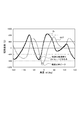
図8は感光ドラム上のトナー載り量、および、感光ドラムの画像領域へのキャリア付着量の現像バイアス依存性(コントラスト電位依存性)を示す図である。図8に示すように、現像バイアス(コントラスト電位)を大きくすると感光ドラム上のトナーの載り量は増えるが、300〜400Vから感光ドラム1aの画像領域へのキャリア付着量も急激に増える。
FIG. 8 is a diagram showing the developing bias dependency (contrast potential dependency) of the toner loading amount on the photosensitive drum and the carrier adhesion amount on the image area of the photosensitive drum. As shown in FIG. 8, when the developing bias (contrast potential) is increased, the amount of toner applied on the photosensitive drum increases, but the carrier adhesion amount from 300 to 400 V to the image area of the
一方、プレバイアスの電圧を大きくすると、同様に電界強度が大きくなるので、現像スリーブ231aと補助電極235aとの間で移動するトナーの量は増える。このとき同時にキャリアの移動が起こったとしても、キャリア粒子の行き先は電極部表面であるため、現像バイアスを大きくしたときとは違い、出力画像には現れない。この為、補助電極235aと現像スリーブ231aとの間に印加する電圧を大きくすることによって、感光ドラム上の画像領域へのキャリア付着のリスクを抑えつつ画像濃度を上げることが可能である。
On the other hand, when the pre-bias voltage is increased, the electric field strength is similarly increased, so that the amount of toner moving between the developing
図9は感光ドラム上のトナー載り量、および、感光ドラムの画像領域へのキャリア付着量のプレバイアス依存性を示す図である。図9の横軸は現像電界Edevに対するプレバイアス電界強度Epreの比である。 FIG. 9 is a diagram showing the pre-bias dependency of the toner loading amount on the photosensitive drum and the carrier adhesion amount on the image area of the photosensitive drum. The horizontal axis of FIG. 9 represents the ratio of the pre -bias electric field strength E pre to the developing electric field E dev .
現像電界に対してプレバイアス電界を大きくすると感光ドラム上のトナーの載り量は増える。プレバイアス電界の大きさが現像電界の大きさ以下であれば、感光ドラム上のトナー載り量の変化はさほど大きくないが、プレバイアス電界の大きさが現像電界の大きさを超えると感光ドラム上トナー載り量が急激に大きくなる。また、プレバイアス電界の大きさを変えても感光ドラム上の画像領域へのキャリア付着量には変化が殆ど無い。 Increasing the pre-bias electric field with respect to the developing electric field increases the amount of toner on the photosensitive drum. If the magnitude of the pre-bias electric field is less than or equal to the magnitude of the developing electric field, the amount of toner applied on the photosensitive drum will not change so much, but if the magnitude of the pre-bias electric field exceeds the magnitude of the developing electric field, The amount of applied toner increases rapidly. Further, even if the magnitude of the pre-bias electric field is changed, there is almost no change in the carrier adhesion amount to the image area on the photosensitive drum.
プレバイアス電界を現像電界よりも大きくすることによってどのような効果が生じるかを明確にするために、二成分AC現像方式と二成分DC現像方式の現像性の違いを次のようなモデルを用いて考察を行なった。 In order to clarify what kind of effect is produced by making the pre-bias electric field larger than the developing electric field, the following model is used for the difference in developability between the two-component AC developing method and the two-component DC developing method. And discussed.
周知の通り、感光ドラム1aと現像スリーブ231aとが対向する現像領域Aにおいて、両者の間に適当な電圧を印加することでトナーが感光ドラム表面に現像され、トナー粒子に作用する力が釣り合った時点で現像は収束する。ここで、トナー粒子に作用する力とは、例えば、現像領域に形成される電界による力やトナーとキャリアとの間の静電的・非静電的な力、等である。
As is well known, in the developing area A where the
AC現像ではDC現像と比較して現像電界の強度が大きいので現像の速度は速く、現像が収束するまでの時間は短い。また、AC現像では現像バイアスの交流成分によるトナーとキャリアの分離効果が大きく、現像に寄与するトナーの量が多いため、現像収束後に最終的に現像されるトナーの量M∞は多い。 In AC development, the intensity of the development electric field is larger than in DC development, so the development speed is fast and the time until development converges is short. In AC development, the toner and carrier separation effect by the AC component of the development bias is large, and the amount of toner that contributes to development is large. Therefore, the amount of toner M ∞ that is finally developed after development convergence is large.
これらのことから、感光ドラム1aに現像されるトナーの量Mを現像時間の関数としてプロットすると図10(a)のようになることが想定される。
From these facts, it is assumed that the amount M of toner developed on the
現像時間を延ばすことは、例えば、現像スリーブ231aや感光ドラム1aの径を大きくする等で現像領域Aにおいて磁気ブラシと感光ドラム1aとが接触する範囲を広くすることによって達成される。以下、本実施形態に於ける現像時間をtdevと表す。
Extending the development time can be achieved, for example, by increasing the contact area between the magnetic brush and the
補助電極235aを用いて現像剤中のトナーを感光ドラム側に寄せることは、現像に寄与するトナーの量を増やすことに相当し、図10(a)に於けるDC現像の曲線を図10(b)の点線のようにシフトさせる効果がある。
Bringing the toner in the developer to the photosensitive drum side using the
前述の通り、現像電界の下で十分に時間をかけて現像を行なった場合、現像スリーブ231aから感光ドラム1aに現像されるトナーの量はM∞である。このことから、プレバイアスによって形成される電界の大きさが現像電界と等しい大きさであれば、プレバイアスによって磁気穂の先端に集められるトナーの量は高々M∞であることがわかる。このため、感光ドラム上に現像されるトナーの量もM∞よりも多くなることはない。つまり、プレバイアスによって形成される電界の大きさが現像電界と等しい大きさであれば、図11(a)に示すように、感光ドラム上に現像されるトナーの量はM∞を超えることはない。実際には、現像剤が補助電極位置を通過する時間および現像時間は有限なので磁気穂Gの先端に集められるトナーの量は更に少ない。
As described above, when subjected to development for a sufficient time under the developing electric field, the amount of toner developed from the developing
しかし、現像電界よりも大きな電界が形成されるようにプレバイアスを印加した場合、通常の現像において感光ドラム上に現像されるトナーの量よりも多くのトナーを磁気穂の先端に集めることが可能になるので、図11(b)に示すように、M∞以上のトナー量を現像させることが可能である。 However, when a pre-bias is applied so that an electric field larger than the developing electric field is formed, it is possible to collect more toner at the tip of the magnetic spike than the amount of toner developed on the photosensitive drum in normal development. since, as shown in FIG. 11 (b), it is possible to develop the toner amount of more than M ∞.
本実施形態において、感光ドラム1a上の静電潜像の暗部電位Vdと明部電位VlはそれぞれVd=−700V、Vl=−300Vである。現像時に現像スリーブ231aに印加される直流電圧は−500Vである。現像時に感光ドラム1aと現像スリーブ231aとの間に印加される電圧は200Vである。感光ドラム1aと現像スリーブ231aとの最も接近する最近接部における感光ドラム1aと現像スリーブ231aの間隔が300μmの場合、感光ドラム1aと現像スリーブ231aとの最近接部において平行平板近似が成り立つとすると、現像電界は6.7×10⁵V/mである。
In this embodiment, the dark potential V d and the light portion potential V l each V d = -700 V of the electrostatic latent image on the photosensitive drum 1a, a V l = -300 V. The DC voltage applied to the developing
また、補助電極235aの電極部236aを接地すると、現像スリーブ231aとの電位差は500Vである。電極部236aを現像スリーブ231aから600μm離して配置した場合、現像スリーブ231aと電極部236aとの間に生じる電界の大きさは8.3×10⁵V/mである。電極部236aを現像スリーブ231aに近づけると電界強度を更に大きくすることは可能であるが、近づけ過ぎると電極部236aと現像スリーブ231aとの間で放電が起きる。放電が起きると、電界がなくなり、トナーの引きつけができなくなってしまう。
Further, when the
そこで、本実施形態では、電極部236aと現像スリーブ231aとの間隔を300〜700μmの間で調整し、この値から放電開始電圧をパッシェンの法則をより計算し、これをプレバイアス電圧の上限とする。
Therefore, in the present embodiment, the interval between the
以上説明したように、本実施形態によれば、現像領域Aの現像剤搬送方向上流側の補助電極235aと現像スリーブ231aとの間に現像電界よりも大きな電界が形成されるようにプレバイアスを印加する。これによって、現像剤表面のトナー濃度を高め、よりいっそう画像濃度を高めることができる。
As described above, according to this embodiment, the pre-bias is applied so that an electric field larger than the developing electric field is formed between the
[第2実施形態]
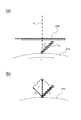
次に本発明に係る現像装置及び画像形成装置の第2実施形態について図を用いて説明する。上記第1実施形態と説明の重複する部分については、同一の符号を付して説明を省略する。図12(a)は磁性板236bを設けない場合の現像スリーブ231aと補助電極235aとの間の磁力線の様子を示す図である。図12(b)は磁性板236bを設けた場合の現像スリーブ231aと補助電極235aとの間の磁力線の様子を示す図である。図13は磁性板236bを設置したときとそうでないときの感光ドラム上のトナー載り量、および、感光ドラム上の画像領域へのキャリア付着量のプレバイアス依存性を示す図である。
[Second Embodiment]
Next, a second embodiment of the developing device and the image forming apparatus according to the present invention will be described with reference to the drawings. The same parts as those in the first embodiment will be denoted by the same reference numerals and the description thereof will be omitted. FIG. 12A is a diagram illustrating a state of magnetic lines of force between the developing
図12(b)に示すように、本実施形態の画像形成装置は、上記第1実施形態の補助電極235aに磁性板236bを取り付けたものである。
As shown in FIG. 12B, the image forming apparatus of the present embodiment is obtained by attaching a
図12(a)に示すように、磁性板236bを設けない場合、バイアス印加範囲内の現像剤搬送方向上流側において、現像剤が十分に穂立っていない部分がある。
As shown in FIG. 12A, when the
図12(b)に示すように、磁性板236bを設けた場合、磁気穂Gの形状は磁界のベクトル場に概ね追従するので、磁性板236bを配置することによってバイアス印加範囲内の磁気穂Gは補助電極235aに対してほぼ垂直に接する。
As shown in FIG. 12 (b), when the
これにより、現像スリーブ上の現像剤は磁気穂Gと磁気穂Gの間に隙間を含んだ状態になるので、トナー粒子がプレバイアスの作用で現像剤中を移動するときに周囲の現像剤等から受ける抵抗が減り、トナーの移動度が上がる。これにより、図13に示すように、プレバイアス印加によりトナーをより効率的に磁気穂Gの先端へと動かすことができる。 As a result, the developer on the developing sleeve is in a state including a gap between the magnetic spike G and the magnetic spike G. Therefore, when the toner particles move through the developer due to the pre-bias, the surrounding developer, etc. The resistance received from the toner decreases and the mobility of the toner increases. As a result, as shown in FIG. 13, the toner can be moved to the tip of the magnetic spike G more efficiently by applying a pre-bias.
すなわち、補助電極235aに磁性板236bを取り付けることによって、バイアス印加範囲内の現像剤を穂立たせ、バイアスによるトナー引き付け効果が得られやすくなり、バイアス印加範囲内の磁力線が補助電極235aに向かうようになる。
That is, by attaching the
A …現像領域
G …磁気穂
H …法線
P …シート
Pa〜Pd …画像形成部
1a …感光ドラム(像担持体)
23a〜23d …現像装置
29 …2次転写内ローラ(転写手段)
231a …現像スリーブ(現像剤担持体)
235a …補助電極
236a …電極部(電極部材)
236b …磁性板
237a …電極支持部材
100 …画像形成装置
A ... Development area G ... Magnetic spike H ... Normal line P ... Sheet Pa to Pd ...
23a to 23d ... developing
231a... Development sleeve (developer carrier)
235a ... auxiliary electrode 236a ... electrode part (electrode member)
236b ...
Claims (5)
前記現像領域よりも現像剤搬送方向上流側に配置された電極部材と、を有し、
前記電極部材と前記像担持体の間にプレバイアスをかけ、
前記現像剤担持体に直流電圧を印加し、前記現像剤担持体と前記像担持体の間に現像バイアスをかけて、前記現像剤担持体上の現像剤中のトナーを前記像担持体へ移動させて、前記像担持体上の静電潜像を現像する現像装置において、
前記プレバイアスによる前記電極部材と前記現像剤担持体との間の電界強度が、前記現像バイアスによる前記像担持体と前記現像剤担持体との間の電界強度よりも大きいことを特徴とする現像装置。
A developer carrier disposed opposite to an image carrier carrying an electrostatic latent image and carrying a developer having toner and a carrier to a development region;
An electrode member disposed on the upstream side in the developer transport direction from the development region,
Apply a pre-bias between the electrode member and the image carrier,
A DC voltage is applied to the developer carrier, a development bias is applied between the developer carrier and the image carrier, and the toner in the developer on the developer carrier is moved to the image carrier. In the developing device for developing the electrostatic latent image on the image carrier,
The development is characterized in that the electric field strength between the electrode member and the developer carrier due to the pre-bias is larger than the electric field strength between the image carrier and the developer carrier due to the development bias. apparatus.
The electrode member has a developer, a photosensitive drum, and a photosensitive drum from a position facing a magnetic pole closest to the developing area among a plurality of magnetic poles inside the developer carrying member positioned upstream of the developing area in the developer conveying direction. The developing device according to claim 1, wherein a pre-bias is applied between the contact positions.
2. The electric field strength between the electrode member and the developer carrier due to the pre-bias is a strength that does not cause discharge between the electrode member and the developer carrier. 2. The developing device according to 2.
前記電極支持部材に、前記現像剤担持体上の現像剤を穂立たせる磁性板が設けられていることを特徴とする請求項1乃至3のいずれか1項に記載の現像装置。
An electrode support member for supporting the electrode member;
4. The developing device according to claim 1, wherein the electrode support member is provided with a magnetic plate that makes the developer on the developer bearing member stand up. 5.
前記現像装置によって現像されたトナー像を記録媒体へ転写する転写手段を有することを特徴とする画像形成装置。 A developing device according to any one of claims 1 to 4,
An image forming apparatus comprising transfer means for transferring a toner image developed by the developing device to a recording medium.
Priority Applications (2)
| Application Number | Priority Date | Filing Date | Title |
|---|---|---|---|
| JP2011013965A JP2012155131A (en) | 2011-01-26 | 2011-01-26 | Developing device and image forming apparatus |
| US13/344,939 US9098011B2 (en) | 2011-01-26 | 2012-01-06 | Development device |
Applications Claiming Priority (1)
| Application Number | Priority Date | Filing Date | Title |
|---|---|---|---|
| JP2011013965A JP2012155131A (en) | 2011-01-26 | 2011-01-26 | Developing device and image forming apparatus |
Publications (1)
| Publication Number | Publication Date |
|---|---|
| JP2012155131A true JP2012155131A (en) | 2012-08-16 |
Family
ID=46544259
Family Applications (1)
| Application Number | Title | Priority Date | Filing Date |
|---|---|---|---|
| JP2011013965A Pending JP2012155131A (en) | 2011-01-26 | 2011-01-26 | Developing device and image forming apparatus |
Country Status (2)
| Country | Link |
|---|---|
| US (1) | US9098011B2 (en) |
| JP (1) | JP2012155131A (en) |
Citations (2)
| Publication number | Priority date | Publication date | Assignee | Title |
|---|---|---|---|---|
| JPH01302283A (en) * | 1988-02-12 | 1989-12-06 | Ricoh Co Ltd | Developing device |
| JPH07333976A (en) * | 1994-06-02 | 1995-12-22 | Konica Corp | Developing device |
Family Cites Families (10)
| Publication number | Priority date | Publication date | Assignee | Title |
|---|---|---|---|---|
| JPS5518631A (en) | 1978-07-28 | 1980-02-08 | Ricoh Co Ltd | Developing and cleaning device in electrophotographic copier and others |
| JPH0470874A (en) | 1990-07-12 | 1992-03-05 | Fuji Xerox Co Ltd | Multicolor image forming device |
| US5428428A (en) * | 1992-06-15 | 1995-06-27 | Konica Corporation | Developing device having a control electrode |
| JP3087541B2 (en) | 1993-11-12 | 2000-09-11 | 富士ゼロックス株式会社 | Developing device |
| JPH07146603A (en) | 1993-11-26 | 1995-06-06 | Fujitsu Ltd | Image forming device |
| JPH07152247A (en) | 1993-11-29 | 1995-06-16 | Konica Corp | Image forming device |
| EP0660200B1 (en) * | 1993-12-24 | 2000-06-14 | Canon Kabushiki Kaisha | Developing apparatus generating electric field between developer carrying member and developer layer regulating member |
| US5602630A (en) * | 1994-09-22 | 1997-02-11 | Konica Corporation | Developing device |
| JPH09236986A (en) | 1996-03-01 | 1997-09-09 | Ricoh Co Ltd | Image forming device |
| JP2014119692A (en) * | 2012-12-19 | 2014-06-30 | Konica Minolta Inc | Developing apparatus and image forming apparatus |
-
2011
- 2011-01-26 JP JP2011013965A patent/JP2012155131A/en active Pending
-
2012
- 2012-01-06 US US13/344,939 patent/US9098011B2/en not_active Expired - Fee Related
Patent Citations (2)
| Publication number | Priority date | Publication date | Assignee | Title |
|---|---|---|---|---|
| JPH01302283A (en) * | 1988-02-12 | 1989-12-06 | Ricoh Co Ltd | Developing device |
| JPH07333976A (en) * | 1994-06-02 | 1995-12-22 | Konica Corp | Developing device |
Also Published As
| Publication number | Publication date |
|---|---|
| US20120189357A1 (en) | 2012-07-26 |
| US9098011B2 (en) | 2015-08-04 |
Similar Documents
| Publication | Publication Date | Title |
|---|---|---|
| JP2006284966A (en) | Image forming apparatus | |
| US8086148B2 (en) | Electrophotographic image forming apparatus | |
| JP3599192B2 (en) | Image forming device | |
| JP4355152B2 (en) | Image developing apparatus, image developing apparatus cleaning method, and image developing method | |
| JP2007322717A (en) | Image forming apparatus | |
| US7308223B2 (en) | Method, device and image forming apparatus for developing an image using a two-component developing agent | |
| JP2015203731A (en) | Developing apparatus, process cartridge, and image forming apparatus | |
| JP2012155131A (en) | Developing device and image forming apparatus | |
| JP2008009178A (en) | Image forming apparatus | |
| JP3400320B2 (en) | One-component developing system | |
| JP6116515B2 (en) | Developing device and image forming apparatus including the same | |
| JP4077202B2 (en) | Image forming apparatus | |
| US11556077B2 (en) | Image formation apparatus | |
| JPH09171287A (en) | Image forming device | |
| JP2009020489A (en) | Developing apparatus and image forming apparatus equipped with the same | |
| JP2002116625A (en) | Image forming device | |
| JP2009069736A (en) | Image forming apparatus | |
| JPH07261547A (en) | Developing device | |
| JP2002287501A (en) | Developing device and image forming device | |
| JP2002278288A (en) | Image forming device | |
| JP6116516B2 (en) | Developing device and image forming apparatus including the same | |
| US8909106B2 (en) | Developing device including blade for regulating a developer layer | |
| JP2015203843A (en) | Developing device and image forming apparatus including the same | |
| JP2010210958A (en) | Developing device and image forming apparatus | |
| JPH10142930A (en) | Developing device |
Legal Events
| Date | Code | Title | Description |
|---|---|---|---|
| A621 | Written request for application examination |
Free format text: JAPANESE INTERMEDIATE CODE: A621 Effective date: 20140117 |
|
| A131 | Notification of reasons for refusal |
Free format text: JAPANESE INTERMEDIATE CODE: A131 Effective date: 20141021 |
|
| A977 | Report on retrieval |
Free format text: JAPANESE INTERMEDIATE CODE: A971007 Effective date: 20141022 |
|
| A521 | Written amendment |
Free format text: JAPANESE INTERMEDIATE CODE: A523 Effective date: 20141219 |
|
| A02 | Decision of refusal |
Free format text: JAPANESE INTERMEDIATE CODE: A02 Effective date: 20150602 |