JP2012150132A - Mechanism for adjusting and fixing light-emitting element, optical scanner, and image forming apparatus - Google Patents
Mechanism for adjusting and fixing light-emitting element, optical scanner, and image forming apparatus Download PDFInfo
- Publication number
- JP2012150132A JP2012150132A JP2011006352A JP2011006352A JP2012150132A JP 2012150132 A JP2012150132 A JP 2012150132A JP 2011006352 A JP2011006352 A JP 2011006352A JP 2011006352 A JP2011006352 A JP 2011006352A JP 2012150132 A JP2012150132 A JP 2012150132A
- Authority
- JP
- Japan
- Prior art keywords
- emitting element
- light emitting
- light
- holding member
- fixing structure
- Prior art date
- Legal status (The legal status is an assumption and is not a legal conclusion. Google has not performed a legal analysis and makes no representation as to the accuracy of the status listed.)
- Granted
Links
Images


Abstract
Description
本発明は、デジタル複写機やレーザプリンタ等の画像形成装置の書込光学系に用いられる光走査装置に関し、特に複数の光ビームを有する発光素子の位置調整及び固定技術に関する。 The present invention relates to an optical scanning device used in a writing optical system of an image forming apparatus such as a digital copying machine or a laser printer, and more particularly to a position adjustment and fixing technique of a light emitting element having a plurality of light beams.
従来、電子写真方式の画像形成においてレーザを光源に用いた画像形成装置が広く知られており、複数本のレーザダイオードから照射されるビームのピッチ調整を行う技術として、レーザダイオードを積載した光源ユニットを回転させて調整を行った後に光源ユニットを光源取付部に対してねじにより固定する技術が、例えば「特許文献1」、「特許文献2」に開示されている。
2. Description of the Related Art Conventionally, an image forming apparatus using a laser as a light source in electrophotographic image formation is widely known. As a technique for adjusting the pitch of a beam emitted from a plurality of laser diodes, a light source unit on which laser diodes are mounted. For example, "
しかし上述の技術では、回転調整時において回転治具により光源取付部の基準面に対して光源ユニットを押し当てる必要があるが、このとき押し当てにより光源取付部に倒れが生じてしまう。このように倒れが生じた状態で調整及び固定を行うと、調整及び固定後に回転治具を外すと光源取付部の倒れが元の状態に戻るため、調整時と固定後とにおいて光源取付部の倒れ量が異なり、光軸に倒れが発生して投射される光の距離及び位置がずれてしまい、書き込み系であれば書き込み画質が低下してしまうという問題点があった。 However, in the above-described technique, it is necessary to press the light source unit against the reference surface of the light source mounting portion with a rotating jig at the time of rotation adjustment. At this time, the light source mounting portion falls down due to the pressing. When adjustment and fixing are performed in such a state where the tilt has occurred, the tilt of the light source mounting part returns to its original state when the rotating jig is removed after adjustment and fixing. There is a problem that the amount of tilting is different, the distance and position of the projected light is shifted due to the tilting of the optical axis, and the writing image quality is lowered in the writing system.
そこで、光源取付部の倒れを防止する技術として、光源ユニットを取り付ける光学箱の側壁に設けられた開口の側傍に補強リブを配置し、これにより光学箱の側壁の剛性を局部的に強化する技術が、例えば「特許文献3」に開示されている。 Therefore, as a technique for preventing the light source mounting portion from collapsing, a reinforcing rib is disposed on the side of the opening provided on the side wall of the optical box to which the light source unit is mounted, thereby locally reinforcing the rigidity of the side wall of the optical box. The technique is disclosed in, for example, “Patent Document 3”.
しかし「特許文献3」に開示された技術では、剛性を局部的に強化するものであって倒れの影響を完全になくすものではなく、感光体上におけるビームピッチの精度は誤差の許容値が数μm以下と極めて厳しく管理しなければならないことから、十分な精度を達成することができなかった。 However, in the technique disclosed in “Patent Document 3”, the rigidity is locally strengthened and the influence of the collapse is not completely eliminated. The accuracy of the beam pitch on the photoconductor has several error tolerances. Sufficient accuracy could not be achieved because it had to be controlled very strictly at μm or less.
本発明は上述の問題点を解決し、調整時と固定時とにおいて発光素子の光軸やビームピッチが変化することを防止することが可能な発光素子の調整固定構造の提供を目的とする。 An object of the present invention is to solve the above-described problems and provide an adjustment fixing structure for a light emitting element capable of preventing the optical axis and beam pitch of the light emitting element from changing during adjustment and fixing.
請求項1記載の発明は、複数の発光点を有する発光素子を前記発光点の光軸周りに回転させることにより前記各発光点間の距離を調整して前記発光素子をハウジングに固定する発光素子の調整固定構造において、前記発光素子が保持部材により保持されると共に前記ハウジングが前記発光素子を取り付ける基準面を有する取付穴及び前記発光素子が前記基準面に当接した状態で回転自在となるように前記保持部材を保持する保持部を有し、前記保持部により前記保持部材を保持した状態で前記発光素子を回転調整した後に前記発光素子を前記ハウジングに固定することを特徴とする。 According to a first aspect of the present invention, a light emitting element that fixes a light emitting element to a housing by adjusting a distance between the light emitting points by rotating a light emitting element having a plurality of light emitting points around an optical axis of the light emitting point. In the adjusting and fixing structure, the light emitting element is held by a holding member, and the housing has a mounting hole having a reference surface to which the light emitting element is attached and the light emitting element is rotatable in a state where the light emitting element is in contact with the reference surface. A holding portion for holding the holding member, and the light emitting device is fixed to the housing after the light emitting device is rotationally adjusted in a state where the holding member is held by the holding portion.
請求項2記載の発明は、請求項1記載の発光素子の調整固定構造において、さらに前記保持部はその厚みが前記ハウジングの厚みに比して十分に薄く形成されていることを特徴とする。 According to a second aspect of the present invention, in the adjustment fixing structure for a light emitting element according to the first aspect, the holding portion is further formed so that the thickness thereof is sufficiently thinner than the thickness of the housing.
請求項3記載の発明は、請求項1または2記載の発光素子の調整固定構造において、さらに前記保持部材は曲折形成されたツバ部を有することを特徴とする。 According to a third aspect of the present invention, in the adjustment fixing structure for a light emitting device according to the first or second aspect, the holding member further has a flange portion formed by bending.
請求項4記載の発明は、請求項1ないし3の何れか1つに記載の発光素子の調整固定構造において、さらに前記保持部材は調整時に用いられる回転治具が取り付けられる取付部を有することを特徴とする。 According to a fourth aspect of the present invention, in the adjustment fixing structure for a light emitting device according to any one of the first to third aspects, the holding member further includes a mounting portion to which a rotating jig used during adjustment is mounted. Features.
請求項5記載の発明は、請求項1ないし4の何れか1つに記載の発光素子の調整固定構造において、さらに前記保持部材は前記発光素子が圧入されることにより前記発光素子を保持することを特徴とする。 According to a fifth aspect of the present invention, in the light-emitting element adjustment fixing structure according to any one of the first to fourth aspects, the holding member further holds the light-emitting element by press-fitting the light-emitting element. It is characterized by.
請求項6記載の発明は、請求項5記載の発光素子の調整固定構造において、さらに前記発光素子は画像ピッチに応じて所定角度傾いた状態で前記保持部材に圧入されることを特徴とする。 According to a sixth aspect of the present invention, in the adjustment fixing structure of the light emitting element according to the fifth aspect, the light emitting element is further press-fitted into the holding member while being inclined at a predetermined angle according to an image pitch.
請求項7記載の発明は、請求項1ないし6の何れか1つに記載の発光素子の調整固定構造を有する光走査装置であることを特徴とする。 A seventh aspect of the invention is an optical scanning device having the light emitting element adjusting and fixing structure according to any one of the first to sixth aspects.
請求項8記載の発明は、請求項7記載の光走査装置を有する画像形成装置であることを特徴とする。 The invention according to claim 8 is an image forming apparatus having the optical scanning device according to claim 7.
本発明によれば、ハウジングの側壁の倒れに起因する走査光線の位置が変化することを防止できるので、光書き込み系であれば走査線の安定性が得られるため良好な画質を得ることができる。 According to the present invention, it is possible to prevent the position of the scanning light beam from being changed due to the tilt of the side wall of the housing, so that if the optical writing system is used, the stability of the scanning line can be obtained, so that good image quality can be obtained. .
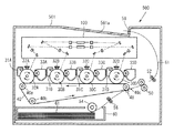
図1は本発明の一実施形態を採用した画像形成装置を示している。同図において画像形成装置500は、光走査装置100、4個の感光体ドラム30A,30B,30C,30D、中間転写ベルト40、給紙トレイ60、給紙ローラ54、レジストローラ対52,56、定着手段50、排紙ローラ対58、図示しない制御手段、装置本体501等を有している。装置本体501の上面には、印刷後の用紙が排出される排紙トレイ501aが設けられており、排紙トレイ501aの下方に光走査装置100が配設されている。光走査装置100は、図示しない画像読取装置あるいは外部装置より送られた画像情報に基づき、感光体ドラム30Aに対して黒色画像成分のレーザ光を、感光体ドラム30Bに対してシアン画像成分のレーザ光を、感光体ドラム30Cに対してマゼンタ画像成分のレーザ光を、感光体ドラム30Dに対してイエロ画像成分のレーザ光をそれぞれ走査する。
FIG. 1 shows an image forming apparatus employing one embodiment of the present invention. In the figure, an
各感光体ドラム30A,30B,30C,30Dは光走査装置100の下方に並設されており、それぞれ図示しない駆動手段により図1において時計回り方向に回転駆動される。感光体ドラム30Aの周囲には、感光体ドラム30Aの表面を所定の電圧で帯電させる帯電手段32A、黒色成分のトナーが充填されたカートリッジ及び現像ローラ等を有する現像手段33A、感光体ドラム30Aの表面に接するクリーニングブレードを有し感光体ドラム30Aの表面をクリーニングするクリーニング手段31Aが配置されている。他の感光体ドラム30B,30C,30Dの周囲にも現像手段に貯容されたトナーの色を除いて同様の構成が配置されており、現像手段33Bにはシアン成分のトナーが、現像手段33Cにはマゼンタ成分のトナーが、現像手段33Dにはイエロ成分のトナーがそれぞれ貯容されている。
The
無端ベルト状の中間転写ベルト40は従動ローラ40a,40c及び駆動ローラ40bに掛け渡されており、その上面が各感光体ドラム30A,30B,30C,30Dと接するように配置されていて、駆動ローラ40bが回転駆動することにより図1の矢印方向に走行駆動される。中間転写ベルト40を介して従動ローラ40cと対向する位置には、帯電手段32A,32B,32C,32Dとは逆極性の電圧を中間転写ベルト40に対して印加する転写手段としての転写チャージャ48が、中間転写ベルト40と所定の距離をおいて近接配置されている。
The endless belt-shaped
中間転写ベルト40の下方には複数枚の用紙61を貯容する給紙トレイ60が配設されており、給紙トレイの図1において右側上方には用紙61を1枚ずつ分離給送する給紙ローラ54が配設されている。給紙ローラ54により給紙トレイ60内より給送された用紙61は、レジストローラ対56を介して転写ベルト40と転写チャージャ48との隙間に向けて給送される。
A sheet feeding tray 60 for storing a plurality of
転写ベルト40と転写チャージャ48との近接部の用紙搬送方向下流側には、加圧ローラと加熱ローラとのローラ対からなる定着手段50が配設されている。定着手段50は熱と圧力とにより用紙61上に転写されたトナー像を定着させ、定着後の用紙61はレジストローラ対52を介して一対のローラ対からなる排紙ローラ対58へと送られ、排紙トレイ501a上に順次排出される。
A
光走査装置100は、図2に示すように、発光素子1から複数の発光点である2本のレーザビームP1,P2を発生させ、各ビームP1,P2をそれぞれコリメートレンズ2によって並行化した上で、シリンドリカルレンズ3を経由して走査手段であるポリゴンミラー4の反射面に照射し、fθレンズ5及び出射窓6を経由して感光体ドラム30に結像させている。このとき感光体ドラム30上に導かれたレーザビームPは、ポリゴンミラー4の回転により主走査方向Q1直交する副走査方向Q2に所定ピッチX1を有する状態で主走査方向Q1に走査される。発光素子1を用いたレーザ走査光学装置では、感光体ドラム30上を多数行にわたって同時走査することにより書き込みが行われる。
As shown in FIG. 2, the
コリメートレンズ2、シリンドリカルレンズ3、ポリゴンミラー4、fθレンズ5等は、装置本体501に取り付けられたオプチカルハウジング7の底壁に取り付けられ、発光素子1はオプチカルハウジング7の側壁7aに取り付けられる。各光学部品をオプチカルハウジング7に取り付けた上で、オプチカルハウジング7の上部開口を図示しない蓋部材によって閉塞する。なお、側壁7aに対する発光素子1の取り付けに関しては後述する。
The collimating lens 2, the cylindrical lens 3, the polygon mirror 4, the
上述した光走査装置100を備えた画像形成装置500の動作を以下に説明する。
外部装置等より画像情報が送られると、発光素子1より射出されたレーザビームP1,P2はコリメートレンズ2、シリンドリカルレンズ3によってポリゴンミラー4の反射面に集光される。ポリゴンミラー4にて偏向されたレーザビームP1,P2は、fθレンズ5を介して感光体ドラム30Aの表面に集光される。同様に、図示しない他の発光素子より射出されたレーザビームがそれぞれポリゴンミラーにより偏向され、他の感光体ドラム30B,30C,30Dの表面にそれぞれ集光される。このとき、光走査装置100からのレーザ光は、予め設定された強度に調整された状態で各感光体ドラム30A〜30Dの書込領域に入射する。
The operation of the
When image information is sent from an external device or the like, the laser beams P1 and P2 emitted from the
各感光体ドラム30A,30B,30C,30Dのそれぞれの表面に設けられた感光層は、帯電手段32A,32B,32C,32Dによって所定の電圧で帯電されることにより電荷が一定の密度で分布している。そして、各感光体ドラム30A,30B,30C,30Dが上述のようにそれぞれ走査されると、レーザ光が集光した部位の感光層が導電性を有するようになり、その部分では電位がほぼゼロとなる。これにより、各感光体ドラム30A,30B,30C,30Dが図1に矢印で示す方向に回転しつつその表面がレーザ光によって走査されると、各感光体ドラム30A,30B,30C,30Dの表面には静電潜像がそれぞれ形成される。
The photosensitive layers provided on the respective surfaces of the
各感光体ドラム30A,30B,30C,30Dの表面にそれぞれ静電潜像が形成されると、各現像手段33A,33B,33C,33Dが有する現像ローラにより各感光体ドラム30A,30B,30C,30Dの表面にそれぞれトナーが供給される。供給されたトナーは各感光体ドラム30A,30B,30C,30D上の静電潜像にそれぞれ静電的に付着し、各静電潜像が各色トナーによって可視像化される。可視像化された各トナー像は中間転写ベルト40の表面に重畳転写され、中間転写ベルト40上にはフルカラートナー像が形成される。形成されたフルカラートナー像は、転写チャージャ48の作動により給紙トレイ60より給送された用紙61の表面に一括転写され、画像が転写された用紙61は定着手段50に送られて転写された画像を定着された後、排紙ローラ対58により排紙トレイ501a上に排出される。
When electrostatic latent images are formed on the surfaces of the
ここで、本発明の特徴部である発光素子1の取り付け構成について説明する。上述した光走査装置100では、感光体ドラム30上に多数行同時に書き込みを行うため、感光体ドラム30上における所定ピッチX1を満たすように発光素子1の回転調整を行う必要がある。この回転調整は、光軸方向を軸として発光素子1を回転させ、これにより発光点間隔を調整する。
Here, the mounting configuration of the light-emitting
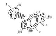
図3に、2ビームの発光素子1を示す。発光素子1は、2つの発光点P1,P2を有するレーザアレイ1aをパッケージングしたものであり、パッケージにはフランジ1bを有しており、フランジ部1bには各発光点P1,P2を結ぶ直線状に2つの切欠部1cが設けられている。この発光素子1を図3に示す矢印R方向に回転調整することにより、所定ピッチX1を満足するように各発光点P1,P2の副走査方向Q2における間隔ΔPを調整する。
FIG. 3 shows a two-beam light-emitting
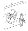
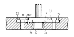
図4に示すように、側壁7aには発光素子1が取り付けられる取付穴13、取付穴13に一体的に形成され発光素子1を取り付ける際に発光素子1を光軸方向に位置決めするための基準面7b、及び側壁7aに一体的に形成された保持部11、円形凹部12、図示しないねじ穴が設けられており、保持部11には図9に示す固定用ねじ10を挿通するための孔11aが穿設されている。円形凹部12は、後述する保持部材21が取付穴13を中心として回転可能となる外径を有しており、保持部11は側壁7aの厚みに比して十分に薄く形成されていて円形凹部12を覆う形状に形成されている。保持部11と円形凹部12との間には、後述する保持部材21のツバ部21bの厚みよりも僅かに大きな隙間が設けられており、保持部11と円形凹部12との間において保持部材21がしっくりと移動可能となるように構成されている。上述した孔11a、図示しないねじ穴、取付穴13は、それぞれ主走査方向Q1と平行する一直線上に位置するように配置されている。
As shown in FIG. 4, a mounting
図5に示すように、発光素子1はそのフランジ部1bを、保持孔21a、2つのツバ部21b、各ツバ部21bに穿設された孔21cを有する保持部材21の保持孔21aに圧入保持されており、発光素子1と保持部材21とにより図4に示す光源ユニット25が構成されている。発光素子1は、フランジ部1bにおける発光側端面(図5において奥側の面)が、保持部材21よりも突出する態様で保持部材21に保持されており、この突出量は円形凹部12と基準面7bとの段差と対応するように構成されている。圧入時において、所定ピッチX1が20μmとなるように、本実施形態では各孔21cの中心を結ぶ直線と各切欠部1cとを結ぶ直線とのなす角度が6〜7°となるように圧入を行う。本形態では6〜7°であるが、所定ピッチX1の設定値によりこの角度は変更される。
As shown in FIG. 5, the light-emitting
次に、側壁7aに対する発光素子1を含む光源ユニット25の取付調整手順を説明する。先ず、光源ユニット25を取付穴13に挿入する。次に、図6に示すように光軸を中心に光源ユニット25を回転させ、図7に示すように各保持部11と円形凹部12との隙間に各ツバ部21bを潜り込ませる。このとき、各保持部11によって各ツバ部21bが押さえられ、フランジ部1bが基準面7bに接触した状態で光源ユニット25が光軸方向に固定される。そして、図8に示すように光源ユニット25を回転治具Jによりチャッキングし、光軸を中心に光源ユニット25を回転させてビーム間隔の調整を行い、調整後に図9に示すように固定用ねじ10によって保持部材21を側壁7aに固定する。固定時において、保持部11の厚みが側壁7aの厚みに対して十分に薄いため、剛性が低いことから固定時における側壁7aの変形が抑制され、固定時に側壁7aが変形することにより光軸が傾くことが防止される。
Next, a procedure for adjusting the attachment of the
上述の構成により、保持部11によって光源ユニット25が基準面7bに当接して位置決めされるため、図10に示す従来のように回転治具によって発光素子1または回転治具自体を側壁7aに押し当てる必要がなく、側壁7aが不要な外力を受けないことから弾性変形せず、ビーム間隔調整時と固定後とにおいて側壁7aの弾性変形がビーム間隔の調整に影響を及ぼすという不具合の発生を防止することができる。
With the above-described configuration, the
上述の構成により、オプチカルハウジングの側壁の倒れに起因する走査光線の位置が変化することを防止できるので、光書き込み系であれば走査線の安定性が得られるため良好な画質を得ることができる。また、発光素子を保持するための治具の機能を回転調整のみに限定できるため、治具の構成を簡易化できコストダウンを図ることができる。 With the above-described configuration, it is possible to prevent the position of the scanning light beam from changing due to the tilt of the side wall of the optical housing. Therefore, if the optical writing system is used, the stability of the scanning line can be obtained, so that a good image quality can be obtained. . In addition, since the function of the jig for holding the light emitting element can be limited to only rotation adjustment, the structure of the jig can be simplified and the cost can be reduced.
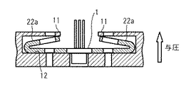
図11は、本発明の上記実施形態の変形例を示している。この変形例では、保持部材21に代えて、折り返されるように曲折形成された2箇所のツバ部22aを有する保持部材22を用い、保持部11と円形凹部12との間の隙間をツバ部22aの厚み(基部と自由端との厚み)よりも小さくなるように形成した点において上記実施形態と相違している。各ツバ部22aには、固定用ねじ10が挿通される孔が各2箇所ずつ形成されている。この変形例によれば、保持部材22を保持部11と円形凹部12との間に潜り込ませた際に、図12に示すように各ツバ部22aによって各保持部11を与圧する機能を有しているため、上記実施例に比して発光素子1を基準面7bに対して確実に押圧することができ、位置決め精度を向上することができる。
FIG. 11 shows a modification of the above embodiment of the present invention. In this modification, instead of the holding
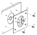
図13は、上記実施形態の他の変形例を示している。この例では、曲折形成された2箇所のツバ部23aと、各ツバ部23aとは別に形成された2箇所の突起部23bとを有し、各突起部23bに固定用ねじ10を挿通するための孔23c及び回転治具Jを取り付けるための取付部23dを形成した保持部材23を用いている。この場合、保持部11は図14に示すような形状とする。この構成とすることにより、曲折形成されたツバ部23aを介することなく光源ユニット25を側壁7aに固定できるため、固定時におけるビーム間隔の変動をより一層低減することができる。
FIG. 13 shows another modification of the above embodiment. In this example, there are two
図15は、上記実施形態のさらに他の変形例を示している。この例では、曲折形成された2箇所のツバ部24aと、各ツバ部24aとは別に曲折形成された2箇所の突起部24bとを有し、各突起部24bに固定用ねじ10を挿通するための孔24c及び回転治具との連結部24dを形成した保持部材24を用いている。この構成により、より簡易な回転治具によるビーム幅の調整が可能となる。
FIG. 15 shows still another modification of the above embodiment. In this example, there are two
上記実施形態及び各変形例ではレーザビームの数を2としたが3以上であってもよく、また、保持部11及びこれに対応したツバ部21b,22a,23a,24aの数を2としたが3以上または1でもよい。また、上記実施形態及び各変形例では側壁7aと一体で保持部11を形成したが、図16に示すように保持部の機能を有する板部材15を側壁7aに固定する構成としてもよい。さらに、本実施形態及び各変形例では保持部材21,22,23,24に対して発光素子1を圧入によって固定しているが、圧入に代えて接着、蝋付け、溶接等の方法によって固定してもよい。さらに、本実施形態及び各変形例では側壁7aに対して光源ユニット25を固定用ねじ10によって固定しているが、これに代えて接着、蝋付け、溶接等の方法によって固定してもよい。
Although the number of laser beams is 2 in the above embodiment and each modification, it may be 3 or more, and the number of holding
1 発光素子
7 ハウジング(オプチカルハウジング)
7b 基準面
7c,7d,7e 取付穴
11 保持部
13 取付穴
21,22,23,24 保持部材
21b,22a,23a,24a ツバ部
23d 取付部
100 光走査装置
500 画像形成装置
P1,P2 発光点(レーザビーム)
1 Light Emitting Element 7 Housing (Optical Housing)
7b Reference surface 7c, 7d, 7e Mounting
Claims (8)
前記発光素子が保持部材により保持されると共に前記ハウジングが前記発光素子を取り付ける基準面を有する取付穴及び前記発光素子が前記基準面に当接した状態で回転自在となるように前記保持部材を保持する保持部を有し、前記保持部により前記保持部材を保持した状態で前記発光素子を回転調整した後に前記発光素子を前記ハウジングに固定することを特徴とする発光素子の調整固定構造。 In a light emitting element adjustment fixing structure in which a light emitting element having a plurality of light emitting points is rotated around an optical axis of the light emitting point to adjust a distance between the light emitting points and fix the light emitting element to a housing.
The light emitting element is held by a holding member, and the holding member is held so that the housing can rotate freely in a state where the light emitting element is in contact with the reference surface and a mounting hole having a reference surface to which the light emitting element is attached. An adjustment fixing structure for a light emitting element, wherein the light emitting element is fixed to the housing after the light emitting element is rotationally adjusted in a state where the holding member is held by the holding part.
前記保持部はその厚みが前記ハウジングの厚みに比して十分に薄く形成されていることを特徴とする発光素子の調整固定構造。 In the adjustment fixing structure of the light emitting element according to claim 1,
The structure of adjusting and fixing a light-emitting element, wherein the holding portion has a thickness sufficiently smaller than a thickness of the housing.
前記保持部材は曲折形成されたツバ部を有することを特徴とする発光素子の調整固定構造。 In the adjustment fixing structure of the light emitting element according to claim 1 or 2,
The holding structure of the light emitting element is characterized in that the holding member has a flange portion formed by bending.
前記保持部材は調整時に用いられる回転治具が取り付けられる取付部を有することを特徴とする発光素子の調整固定構造。 In the adjustment fixing structure of the light emitting element as described in any one of Claims 1 thru | or 3,
The light-emitting element adjustment fixing structure, wherein the holding member has an attachment portion to which a rotating jig used for adjustment is attached.
前記保持部材は前記発光素子が圧入されることにより前記発光素子を保持することを特徴とする発光素子の調整固定構造。 In the adjustment fixing structure of the light emitting element according to any one of claims 1 to 4,
The light-emitting element adjusting and fixing structure, wherein the holding member holds the light-emitting element by press-fitting the light-emitting element.
前記発光素子は画像ピッチに応じて所定角度傾いた状態で前記保持部材に圧入されることを特徴とする発光素子の調整固定構造。 In the adjustment fixing structure of the light emitting element according to claim 5,
The light-emitting element adjusting and fixing structure, wherein the light-emitting element is press-fitted into the holding member while being inclined at a predetermined angle according to an image pitch.
Priority Applications (3)
| Application Number | Priority Date | Filing Date | Title |
|---|---|---|---|
| JP2011006352A JP5678675B2 (en) | 2011-01-14 | 2011-01-14 | Adjusting and fixing structure of light emitting element, optical scanning device, and image forming apparatus |
| US13/349,960 US8911112B2 (en) | 2011-01-14 | 2012-01-13 | Light emitting element adjusting and fixing structure, optical scanner, and image forming apparatus |
| CN201210031838.8A CN102591011B (en) | 2011-01-14 | 2012-01-16 | Light emitting element adjusting and fixing structure, optical scanner, and image forming apparatus |
Applications Claiming Priority (1)
| Application Number | Priority Date | Filing Date | Title |
|---|---|---|---|
| JP2011006352A JP5678675B2 (en) | 2011-01-14 | 2011-01-14 | Adjusting and fixing structure of light emitting element, optical scanning device, and image forming apparatus |
Publications (2)
| Publication Number | Publication Date |
|---|---|
| JP2012150132A true JP2012150132A (en) | 2012-08-09 |
| JP5678675B2 JP5678675B2 (en) | 2015-03-04 |
Family
ID=46792465
Family Applications (1)
| Application Number | Title | Priority Date | Filing Date |
|---|---|---|---|
| JP2011006352A Expired - Fee Related JP5678675B2 (en) | 2011-01-14 | 2011-01-14 | Adjusting and fixing structure of light emitting element, optical scanning device, and image forming apparatus |
Country Status (1)
| Country | Link |
|---|---|
| JP (1) | JP5678675B2 (en) |
Cited By (3)
| Publication number | Priority date | Publication date | Assignee | Title |
|---|---|---|---|---|
| JP2012155100A (en) * | 2011-01-25 | 2012-08-16 | Ricoh Co Ltd | Light-emitting element adjusting and fixing structure, optical scanner, and image forming apparatus |
| JP2014130314A (en) * | 2012-11-27 | 2014-07-10 | Ricoh Co Ltd | Optical scanner and image forming apparatus |
| JP2016133777A (en) * | 2015-01-22 | 2016-07-25 | キヤノン株式会社 | Optical scanner and image forming apparatus including the optical scanner |
Citations (7)
| Publication number | Priority date | Publication date | Assignee | Title |
|---|---|---|---|---|
| JPH1158829A (en) * | 1997-08-26 | 1999-03-02 | Canon Inc | Laser beam source apparatus |
| JP2000089147A (en) * | 1998-09-14 | 2000-03-31 | Canon Inc | Multi-beam scanner |
| JP2003066357A (en) * | 2001-08-23 | 2003-03-05 | Ricoh Co Ltd | Optical scanner and image forming device |
| JP2005024721A (en) * | 2003-06-30 | 2005-01-27 | Ricoh Co Ltd | Deflection mirror, optical scanner and image formation device |
| JP2005093975A (en) * | 2003-09-19 | 2005-04-07 | Samsung Electro-Mechanics Co Ltd | Semiconductor laser diode apparatus with pcb type lead frame |
| JP2006072292A (en) * | 2004-08-06 | 2006-03-16 | Ricoh Co Ltd | Optical scanning unit/image forming apparatus |
| JP2007286386A (en) * | 2006-04-18 | 2007-11-01 | Konica Minolta Business Technologies Inc | Laser scanner |
-
2011
- 2011-01-14 JP JP2011006352A patent/JP5678675B2/en not_active Expired - Fee Related
Patent Citations (7)
| Publication number | Priority date | Publication date | Assignee | Title |
|---|---|---|---|---|
| JPH1158829A (en) * | 1997-08-26 | 1999-03-02 | Canon Inc | Laser beam source apparatus |
| JP2000089147A (en) * | 1998-09-14 | 2000-03-31 | Canon Inc | Multi-beam scanner |
| JP2003066357A (en) * | 2001-08-23 | 2003-03-05 | Ricoh Co Ltd | Optical scanner and image forming device |
| JP2005024721A (en) * | 2003-06-30 | 2005-01-27 | Ricoh Co Ltd | Deflection mirror, optical scanner and image formation device |
| JP2005093975A (en) * | 2003-09-19 | 2005-04-07 | Samsung Electro-Mechanics Co Ltd | Semiconductor laser diode apparatus with pcb type lead frame |
| JP2006072292A (en) * | 2004-08-06 | 2006-03-16 | Ricoh Co Ltd | Optical scanning unit/image forming apparatus |
| JP2007286386A (en) * | 2006-04-18 | 2007-11-01 | Konica Minolta Business Technologies Inc | Laser scanner |
Cited By (3)
| Publication number | Priority date | Publication date | Assignee | Title |
|---|---|---|---|---|
| JP2012155100A (en) * | 2011-01-25 | 2012-08-16 | Ricoh Co Ltd | Light-emitting element adjusting and fixing structure, optical scanner, and image forming apparatus |
| JP2014130314A (en) * | 2012-11-27 | 2014-07-10 | Ricoh Co Ltd | Optical scanner and image forming apparatus |
| JP2016133777A (en) * | 2015-01-22 | 2016-07-25 | キヤノン株式会社 | Optical scanner and image forming apparatus including the optical scanner |
Also Published As
| Publication number | Publication date |
|---|---|
| JP5678675B2 (en) | 2015-03-04 |
Similar Documents
| Publication | Publication Date | Title |
|---|---|---|
| US7830576B2 (en) | Scanning optical apparatus and method, and image forming apparatus | |
| JP6489410B2 (en) | Optical scanning apparatus and image forming apparatus | |
| JP2006323159A (en) | Optical scanner and image forming apparatus | |
| JP5397328B2 (en) | Image forming apparatus | |
| US8872873B2 (en) | Light scanning unit and image forming apparatus using the same | |
| JP5678675B2 (en) | Adjusting and fixing structure of light emitting element, optical scanning device, and image forming apparatus | |
| JP2011053467A (en) | Optical scanning device and image forming apparatus equipped with the same | |
| JP2007133320A (en) | Optical scanning apparatus and image forming apparatus | |
| EP2875957A1 (en) | Multibeam light source unit, method of adjusting the same, light scanning unit, and electrophotography type image forming apparatus | |
| US8717640B2 (en) | Optical scanner and image forming apparatus including same | |
| JP5821195B2 (en) | Adjusting and fixing structure of light emitting element, optical scanning device, and image forming apparatus | |
| JP6184285B2 (en) | Optical scanning device and image forming apparatus including the optical scanning device | |
| JP6848293B2 (en) | Optical scanning device and image forming device | |
| JP2006337515A (en) | Optical scanner and image forming apparatus | |
| JP6192274B2 (en) | Optical scanning apparatus and image forming apparatus | |
| JP2011095458A (en) | Optical scanner and image forming apparatus equipped with the same | |
| JP5743539B2 (en) | Image forming apparatus | |
| JP6413904B2 (en) | Optical scanning device and image forming apparatus | |
| JP6610875B2 (en) | Optical scanning device and image forming apparatus | |
| JP2008139347A (en) | Optical scanning optical apparatus | |
| JP5966551B2 (en) | Optical scanning apparatus and image forming apparatus | |
| JP2017116601A (en) | Optical scanner and image formation device | |
| JP6281473B2 (en) | Manufacturing method of optical scanning device | |
| JP5799507B2 (en) | Optical scanning apparatus and image forming apparatus | |
| JP5084488B2 (en) | Optical scanning apparatus and image forming apparatus |
Legal Events
| Date | Code | Title | Description |
|---|---|---|---|
| A621 | Written request for application examination |
Free format text: JAPANESE INTERMEDIATE CODE: A621 Effective date: 20131202 |
|
| A977 | Report on retrieval |
Free format text: JAPANESE INTERMEDIATE CODE: A971007 Effective date: 20140416 |
|
| A131 | Notification of reasons for refusal |
Free format text: JAPANESE INTERMEDIATE CODE: A131 Effective date: 20140520 |
|
| A521 | Written amendment |
Free format text: JAPANESE INTERMEDIATE CODE: A523 Effective date: 20140722 |
|
| TRDD | Decision of grant or rejection written | ||
| A01 | Written decision to grant a patent or to grant a registration (utility model) |
Free format text: JAPANESE INTERMEDIATE CODE: A01 Effective date: 20141209 |
|
| A61 | First payment of annual fees (during grant procedure) |
Free format text: JAPANESE INTERMEDIATE CODE: A61 Effective date: 20141222 |
|
| R151 | Written notification of patent or utility model registration |
Ref document number: 5678675 Country of ref document: JP Free format text: JAPANESE INTERMEDIATE CODE: R151 |
|
| LAPS | Cancellation because of no payment of annual fees |