JP2012129429A - Plasma processing method - Google Patents
Plasma processing method Download PDFInfo
- Publication number
- JP2012129429A JP2012129429A JP2010281121A JP2010281121A JP2012129429A JP 2012129429 A JP2012129429 A JP 2012129429A JP 2010281121 A JP2010281121 A JP 2010281121A JP 2010281121 A JP2010281121 A JP 2010281121A JP 2012129429 A JP2012129429 A JP 2012129429A
- Authority
- JP
- Japan
- Prior art keywords
- etching
- frequency power
- wafer
- time
- plasma
- Prior art date
- Legal status (The legal status is an assumption and is not a legal conclusion. Google has not performed a legal analysis and makes no representation as to the accuracy of the status listed.)
- Pending
Links
Images


Abstract
Description
本発明はプラズマ処理方法に係り、特に半導体素子等の試料を加工するために、プラズマを用い且つ試料にエッチング処理を施すのに好適なプラズマ処理方法に関するものである。 The present invention relates to a plasma processing method, and more particularly to a plasma processing method suitable for using plasma and etching a sample to process a sample such as a semiconductor element.
従来、シリコンウエハ上に作製された半導体素子の表面を処理する方法として、半導体素子をプラズマでエッチングする装置が知られている。ここでは、ECR(電子サイクロトロン共鳴)方式と呼ばれる装置を例に、従来技術を説明する。この方式では、外部より磁場を印加した真空容器中でマイクロ波によりプラズマを発生する。磁場により電子はサイクロトロン運動し、この周波数とマイクロ波の周波数を共鳴させることで効率よくプラズマを生成できる。半導体素子に入射するイオンを加速するため、高周波バイアスを概略正弦波にて連続波形で印加している。プラズマとなるガスには塩素やフッ素などのハロゲンガスが広く使われている。 2. Description of the Related Art Conventionally, as a method for treating the surface of a semiconductor element manufactured on a silicon wafer, an apparatus for etching a semiconductor element with plasma is known. Here, the prior art will be described using an apparatus called an ECR (electron cyclotron resonance) system as an example. In this method, plasma is generated by microwaves in a vacuum container to which a magnetic field is applied from the outside. Electrons perform cyclotron motion by a magnetic field, and plasma can be generated efficiently by resonating this frequency with the frequency of microwaves. In order to accelerate ions incident on the semiconductor element, a high-frequency bias is applied in a continuous waveform as an approximate sine wave. A halogen gas such as chlorine or fluorine is widely used as a plasma gas.
プラズマにより発生したラジカルやイオンと被エッチング材が反応することでエッチングが進行する。 Etching progresses by the reaction of radicals and ions generated by plasma with the material to be etched.
エッチングによって発生する反応生成物はウエハへの再付着を引き起こす。反応生成物の再付着はエッチングの阻害によるエッチストップや、パターンへの付着によるエッチング形状のテーパー化を引き起こす。ウエハ上の反応生成物分布が不均一である場合は、部分的にエッチストップやテーパー形状が発生し、エッチング加工形状の不均一化を招く。エッチング装置の場合、真空状態を保つために排気を行いながら処理を行う。このため排気方向に向かってウエハ上の反応生成物が少なくなり、不均一を発生させる要因となる。エッチング装置の構造上、排気による反応生成物の不均一性は避けるのが困難という問題がある。よって、加工の高均一化をはかるためには、反応生成物の不均一の影響を排除できるよう反応生成物やイオンエネルギーを制御し、エッチングを行う必要がある。反応生成物の影響を少なくする手段としては、反応生成物濃度を少なくする方法がある。反応生成物の滞在時間を短くすることで、反応生成物濃度を下げることができる。プラズマ処理室内のガスの滞在時間τはPを圧力、Vを処理室容量、Qをガス流量とした場合、τ=PV/Qの関係があり、装置構成で前記P,V,Qの限界が規定される。この関係からガスとなった反応生成物の滞在時間は圧力を下げることやガス流量の増加で短くすることができるが、真空ポンプの排気速度には限界があるので、ガス流量を増加するのと、処理圧力を下げることはトレードオフの関係にあり改善が困難である。 Reaction products generated by etching cause redeposition to the wafer. The reattachment of the reaction product causes an etch stop due to the inhibition of etching and a tapering of the etching shape due to the adhesion to the pattern. If the reaction product distribution on the wafer is non-uniform, an etch stop or a taper shape is partially generated, resulting in non-uniform etching processing shape. In the case of an etching apparatus, processing is performed while exhausting in order to maintain a vacuum state. For this reason, reaction products on the wafer are reduced in the exhaust direction, which causes non-uniformity. Due to the structure of the etching apparatus, there is a problem that it is difficult to avoid non-uniformity of reaction products due to exhaust. Therefore, in order to achieve high processing uniformity, it is necessary to perform etching while controlling the reaction product and ion energy so as to eliminate the influence of non-uniformity of the reaction product. As a means for reducing the influence of the reaction product, there is a method of reducing the concentration of the reaction product. The reaction product concentration can be lowered by shortening the residence time of the reaction product. The residence time τ of the gas in the plasma processing chamber has a relationship of τ = PV / Q where P is pressure, V is processing chamber capacity, and Q is gas flow rate. It is prescribed. From this relationship, the residence time of the reaction product that has become a gas can be shortened by lowering the pressure or increasing the gas flow rate. However, since the exhaust speed of the vacuum pump is limited, increasing the gas flow rate Lowering the processing pressure is in a trade-off relationship and is difficult to improve.
また、反応生成物堆積によるエッチング阻害を防ぐ方法としては、イオンエネルギーを高くすることがある。印加電力を高くすることでイオンエネルギーを高くできるが、エッチング速度も速くなるため、反応生成物濃度が上がることになり、反応生成物の不均一性が大きくなる。また、この方法では、エッチングレートと反応生成物密度を独立して制御できなくなるため、エッチングレートを均一且つ高精度に制御できないという問題があった。 As a method of preventing etching inhibition due to reaction product deposition, ion energy may be increased. Although the ion energy can be increased by increasing the applied power, the etching rate is also increased, so that the concentration of the reaction product is increased and the non-uniformity of the reaction product is increased. In addition, this method has a problem in that the etching rate and the reaction product density cannot be controlled independently, so that the etching rate cannot be controlled uniformly and with high accuracy.
イオンエネルギーと反応生成物の制御方法として特許文献1にはプラズマやバイアスの時間変調が開示されている。また、一般的には特許文献2に示されるようにバイアスの時間変調のデューティー比は5%以上80%以下の範囲で調整される。 As a method for controlling ion energy and reaction products, Patent Document 1 discloses time modulation of plasma and bias. In general, as shown in Patent Document 2, the duty ratio of bias time modulation is adjusted in a range of 5% to 80%.
半導体素子の微細化及びウエハの大口径化に伴い、薄膜を高均一に且つ精度良く加工する要求が増えている。薄膜エッチングでは、概してエッチング時間が短くなるため、エッチングの終点判定が困難となり、エッチング加工精度が悪くなる問題があった。エッチングの終点判定が困難であることに関してはエッチングレートを低くすることで解決できるが、エッチングレートを低くするためには印加電力を低くし、イオンエネルギーを下げることが必要である。イオンエネルギーを下げると堆積した反応生成物を除去することができなくなり、エッチング反応が阻害される。また反応生成物がウエハ上で不均一な場合には、反応生成物の堆積が多いエリアはエッチングが進行せず、堆積が少ないエリアはエッチングが進行するため、エッチングレートがウエハ面内で不均一になる。イオンエネルギーを高くすることで、堆積した反応生成物によるエッチング阻害の影響を小さくすることができる。これはイオンエネルギーを高くすることでエッチング阻害層を除去し、エッチングを進行させることができるようになるためである。イオンエネルギーを高くするためには、印加する高周波電力を高くする方法が用いられるが、この場合、エッチングレートが速くなり、薄膜エッチングには不適である。反応生成物濃度を下げることで不均一性の影響を緩和することができるが、前述のガス流量と処理圧力のトレードオフの関係から、改善が困難である。 With the miniaturization of semiconductor elements and the increase in diameter of wafers, there is an increasing demand for processing thin films with high uniformity and accuracy. In the thin film etching, since the etching time is generally shortened, it is difficult to determine the end point of etching, and there is a problem that the etching processing accuracy is deteriorated. The difficulty in determining the end point of etching can be solved by lowering the etching rate, but in order to lower the etching rate, it is necessary to lower the applied power and lower the ion energy. When ion energy is lowered, deposited reaction products cannot be removed, and the etching reaction is hindered. If the reaction product is non-uniform on the wafer, etching does not proceed in areas where there is a large amount of reaction product deposition, and etching proceeds in areas where there is little deposition. become. By increasing the ion energy, the influence of etching inhibition by the deposited reaction product can be reduced. This is because the etching inhibition layer can be removed and the etching can be advanced by increasing the ion energy. In order to increase the ion energy, a method of increasing the applied high-frequency power is used. However, in this case, the etching rate becomes high and is not suitable for thin film etching. Although the influence of non-uniformity can be mitigated by reducing the reaction product concentration, it is difficult to improve due to the trade-off relationship between the gas flow rate and the processing pressure described above.
また、印加高周波電力を高くするとイオンエネルギーが高くなり、エッチングレートが高くなる。結果として反応生成物濃度が上がるため、高イオンエネルギーと反応生成物濃度低減はトレードオフの関係にある。また、従来の時間変調を用いた方法では、反応種の制御を行い選択比向上やエッチング加工形状の制御を行うことは可能であるが、ウエハ面内のエッチングレートを高均一で且つ低エッチングレートを実現することが困難であるという問題があった。 Further, when the applied high frequency power is increased, the ion energy is increased and the etching rate is increased. As a result, the reaction product concentration increases, so there is a trade-off between high ion energy and reduction of the reaction product concentration. In addition, in the conventional method using time modulation, it is possible to improve the selection ratio and control the etching processing shape by controlling the reactive species, but the etching rate in the wafer surface is highly uniform and the etching rate is low. There was a problem that it was difficult to realize.
このトレードオフの関係を改善し、高イオンエネルギー且つ低反応生成物濃度の低エッチングレート技術が実現できれば、高均一で高精度な薄膜エッチングが可能となる。 If this trade-off relationship can be improved and a low etching rate technique with high ion energy and low reaction product concentration can be realized, highly uniform and highly accurate thin film etching can be performed.
本発明の目的は低エッチングレートと高均一性を両立するプラズマ処理方法を提供することにある。 An object of the present invention is to provide a plasma processing method that achieves both a low etching rate and high uniformity.
本発明は、薄膜を有する試料の前記薄膜をプラズマエッチングするプラズマ処理方法において、Anm厚さの薄膜を4×Anm/min未満の低エッチングレートでプラズマエッチングし、該プラズマエッチングは前記試料を載置する試料台に時間変調された間欠の高周波電力を印加してプラズマエッチングし、前記高周波電力の1周期での印加していない時間は、1周期での印加している時間より4倍〜100倍長いことを特徴とするプラズマ処理方法である。 The present invention provides a plasma processing method of plasma etching a thin film of a sample having a thin film, wherein the thin film having an nm thickness is subjected to plasma etching at a low etching rate of less than 4 × Anm / min, and the plasma etching is performed by mounting the sample. Plasma etching is performed by applying time-modulated intermittent high-frequency power to a sample stage to be performed, and the time during which the high-frequency power is not applied in one cycle is 4 to 100 times that applied in one cycle. The plasma processing method is characterized by being long.
本発明により、低エッチングレートと高均一性を両立するプラズマ処理を行うことができる。 According to the present invention, it is possible to perform plasma processing that achieves both a low etching rate and high uniformity.
以下、本発明を実施するための形態を説明する。以下、本発明の一実施例で使用するマイクロ波ECR(Electron Cyclotron Resonance)エッチング装置を図1により説明する。上部が開放された真空容器101の上部に、真空容器101内にエッチングガスを導入するためのシャワープレート102(例えば石英製),誘電体窓103(例えば石英製)を設置し、密封することにより処理室104を形成する。シャワープレート102にはエッチングガスを流すためのガス供給装置105が接続される。また、真空容器101には排気用開閉バルブ117及び排気速度可変バルブ108を介し真空排気装置106が接続されている。処理室104内は排気用開閉バルブ117を開とし、真空排気装置106を駆動することで減圧され、真空状態となる。処理室104内の圧力は排気速度可変バルブ118により所望の圧力に調整される。エッチングガスは、ガス供給装置105からシャワープレート102を介して処理室104内に導入され、排気速度可変バルブ118を介して真空排気装置106によって排気される。また、シャワープレート102に対向して真空容器101の下部には試料台であるウエハ載置用電極111が設けられる。
Hereinafter, modes for carrying out the present invention will be described. A microwave ECR (Electron Cyclotron Resonance) etching apparatus used in an embodiment of the present invention will be described below with reference to FIG. By installing and sealing a shower plate 102 (for example, made of quartz) and a dielectric window 103 (for example, made of quartz) for introducing an etching gas into the
プラズマを生成するための電力を処理室104に伝送するため、誘電体窓103の上方には電磁波を伝送する導波管107が設けられる。導波管107へ伝送される電磁波は電磁波発生用電源109から発振させる。電磁波の周波数は特に限定されないが、本実施例では2.45GHzのマイクロ波を使用する。処理室104の外周部には、磁場を形成する磁場発生用コイル110が設けてあり、電磁波発生用電源109より発振された電力は、形成された磁場との相互作用により、処理室104内に高密度プラズマを生成し、ウエハ載置用電極111上に載置された試料であるウエハ112にエッチングを施す。シャワープレート102,ウエハ載置用電極111,磁場発生用コイル110,排気用開閉バルブ117,排気速度可変バルブ118及びウエハ112は処理室104の中心軸上に対して同軸に配置されているため、エッチングガスの流れやプラズマにより生成されたラジカル及びイオン、更にエッチングにより生成された反応生成物はウエハ112に対し同軸に導入,排気される。この同軸配置はエッチングレート,エッチング形状のウエハ面内均一性を軸対称に近づけ、ウエハ処理均一性を向上させる効果がある。ウエハ載置用電極111は電極表面が溶射膜(図示省略)で被覆されており、高周波フィルタ115を介して直流電源116が接続されている。さらに、ウエハ載置用電極111には、マッチング回路113を介して高周波電源114が接続される。また、高周波電源114には、時間変調された間欠の高周波電力をウエハ載置用電極111に印加するため、任意波形発生装置(図示せず)が接続されている。このため、高周波電源114は、ウエハ載置用電極111に印加する高周波電力を時間的に変調して、間欠に供給することも可能となっている。また、時間的に変調された間欠な高周波電力のウエハ載置用電極111への印加時間と印加しない時間の比、およびその印加する周期等は、マイクロ波ECRエッチング装置のエッチング条件(レシピ)に設定され、任意に制御可能となっている。
In order to transmit electric power for generating plasma to the
高周波電源114によりウエハ112に印加される高周波電力の波形を図2に示す。高周波電力波形は高周波電力を印加する期間(オン期間)と印加しない期間(オフ期間)、オフ期間からオン期間への遷移期間1,オン期間からオフ期間への遷移期間2から構成され、それぞれの期間を0〜1秒の範囲で調整できる。高周波電力のオン期間とオフ期間の切り替え時に整合不良などの問題等が発生した場合、前記遷移期間1及び遷移期間2を調整することにより整合不良等の問題を回避できる。遷移期間1及び遷移期間2の設定値としては0.1μs以上とすることで整合エラー発生のポテンシャルを低下させることができる。
The waveform of the high frequency power applied to the
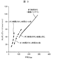
次に上述したマイクロ波ECRエッチング装置を用いて、薄膜の多結晶シリコン膜が成膜されたウエハ112をエッチングした場合の多結晶シリコンのエッチングレートの均一性を向上させるエッチング方法について説明する。本実施例では、上記薄膜の多結晶シリコン膜が成膜されたウエハ112としては直径300mmのシリコンウエハ上に熱酸化膜を成長させた後、20nmの厚さの多結晶シリコン膜を堆積させたものを用いた。一般にエッチングの終点判定はプラズマからの発光をモニタし、発光の変化から被エッチング膜のエッチングの終了した時間を判定する方法が使用されている。概して、エッチング開始時は、プラズマの着火からの密度安定までに時間を要することや、処理圧力調整にも時間を要することで、プラズマの発光が不安定である。よって、エッチング時間が短い場合には、プラズマ発光が不安定でエッチング終点判定の精度が悪くなることがある。このため、エッチングの終点判定を高精度に行うためには、現状、15秒以上のエッチング時間が必要である。このため、被エッチング膜が20nmの膜厚の場合、エッチングレートを80nm/min未満にする必要がある。エッチングレートを下げるためにはウエハ112に印加される高周波電力を小さくすることで、イオンにかかる加速電圧(Vpp)を低くし、イオンエネルギーを低くする必要がある。図3に示すようにウエハ112に印加される高周波電力の時間変調された間欠の1周期平均のVppを低くすることでエッチングレートを低くできる。ここでVppとは、ウエハ112に印加される高周波電圧の最小電圧のピーク値と最大電圧のピーク値の差の電圧であり、ウエハ載置用電極111の表面膜の絶縁破壊が発生しないようにするため、3000V以下が適当である。また、Vppが20V以下ではイオンエネルギーが小さすぎてエッチングが進行しない。そのため、Vppの制御としては最大値を20V以上3000V以下とすることが適当である。また、Vppの調整方法としては、ウエハ載置用電極111へ印加される高周波電力を調整する方法があるが、この場合も、ウエハ載置用電極111の表面膜の絶縁破壊を抑えるために、印加電力を4.3W/cm2以下が適当である。またエッチングが進行するためには印加電力は0.007W/cm2以上程度必要であるため、ウエハ載置用電極111に印加される高周波電力の制御範囲は0.007W/cm2から4.3W/cm2までとすることが望ましい。
Next, an etching method for improving the uniformity of the etching rate of polycrystalline silicon when the
上述のことから、まず、ウエハ載置用電極111に印加される高周波電力の時間変調された間欠の1周期平均電力をエッチングレートが80nm/min未満になるような電力に設定する。次にウエハ載置用電極111に印加される時間変調された間欠の高周波電力の印加しない時間を印加する時間の4倍〜100倍とする。このような時間変調された間欠の高周波電力をウエハ載置用電極に印加して20nm厚さの多結晶シリコン膜が成膜されたウエハ112をエッチングすることにより、図4に示すように80nm/min未満のエッチングレートでウエハ面内均一性を5%以下にすることができ、ウエハ載置用電極111に印加される時間変調された間欠の高周波電力の印加しない時間を印加する時間の19倍〜100倍とすると、ウエハ面内均一性をさらに向上させることができた。
From the above, first, the intermittent one-cycle average power of time-modulated high frequency power applied to the
ウエハ載置用電極111に印加される時間変調された間欠の高周波電力の印加しない時間を印加する時間の4倍〜100倍または、19倍〜100倍にすることにより、低エッチングレートと高均一性を両立できる推定メカニズムは以下の通りである。
A low etching rate and a high uniformity can be obtained by setting the time during which the time-modulated intermittent high-frequency power applied to the
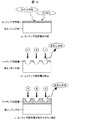
エッチング中のウエハ表面の状態を単純化したモデルを図5に示す。エッチング中にウエハ表面で、図5(a)のようにラジカルや反応生成物の堆積によるエッチング阻害層の形成と図5(b)のようなエッチング阻害層の除去が行われることにより、エッチングが進行する。しかしながら、図5(c)に示すように、エッチング阻害層が非常に厚い場合や、イオンエネルギーが小さくエッチング阻害層を除去できない場合においては、エッチングは進行しない。ウエハ上の反応生成物密度分布は、ウエハ中心上で高く、ウエハ端部に近づくほど低くなる。これは、ウエハ載置用電極111下方に排気装置が配置されており、ウエハ載置用電極111の端部は中心に比べ排気されやすいためである。よって、ウエハ上に堆積する反応生成物はエッチング阻害層となり、その膜厚はウエハ中心で厚く、ウエハ端に近づくにつれて薄くなる分布を持つ。このエッチング阻害層の分布から、ウエハ中心付近では図5(c)に示すエッチングが進行しない状態、ウエハ端付近では図5(b)のエッチングが進行する状態とウエハ中心とウエハ端部付近でエッチングの進行し易さに差が生じることになる。よって、エッチングレート分布はウエハ端部付近でエッチングレートが高く、ウエハ中心でエッチングレートが低くなる。イオンエネルギーが低い場合はエッチング阻害層の膜厚が厚い場合は、エッチング進行に対するウエハ上のエッチング阻害層の影響が大きい。エッチングレートを下げるためには、概してイオンエネルギーを低くする必要があるため、低エッチングレートの場合は、エッチング阻害層のウエハ面内膜厚差の影響を受けやすく、エッチングレートを低くすることとエッチングレート均一性を良くすることを両立することが困難である。エッチングレートを低くすることとエッチングレート均一性を良くすることを両立するためには、反応生成物密度を少なくし、且つ、エッチング阻害層が除去できるようにイオンエネルギーを十分高くすればよい。反応生成物密度を少なくする方法としては、ウエハ載置用電極111に印加する高周波電力を減少させ、エッチングレートを低くすることで単位時間当たりに発生する反応生成物量を少なくする方法がある。しかし、従来方式である連続バイアスで高周波電力を印加する場合、エッチングレートを下げるためには印加高周波電力を低くする必要がある。印加高周波電力が低い場合には、ウエハにかかる電圧(Vpp)が低くなり、イオンエネルギーが低くなる。その結果、ウエハ上のエッチング阻害層の膜厚不均一性の影響を受けやすくなり、エッチングレート均一性が悪くなる。また、印加する連続バイアスの高周波電力を減少させる方法は、前述のエッチング阻害層が除去できるようにイオンエネルギーを十分高くするという方法と相反する方法となる。一方、図2に示す時間変調された間欠の高周波電力をウエハ載置用電極111に印加した場合、イオンエネルギーをエッチング阻害層除去できる値に制御することで、印加している期間にはエッチングが進行する。即ち、印加している期間は図5(b)の状態と言える。印加していない期間にはエッチング阻害層が形成され、同時に印加している期間に発生した反応生成物は排気され、ウエハ上の反応生成物密度は低くなる。また、連続バイアスの高周波電力を印加する場合は反応生成物濃度はエッチング開始時よりエッチング時間の増加に伴って増加していく。一方、時間変調された間欠の高周波電力を印加する場合は、印加している期間内に発生した反応生成物は印加しない期間内に排気され、残留しないため、反応生成物濃度が低い状態を作り出すことが可能である。印加している期間に対してし印加しない期間を長くしていくことで反応生成物密度を低くすることができる。本発明では、図2に示す時間変調された間欠の高周波電力をウエハ載置用電極111に印加しており、この時間変調された間欠の高周波電力の電圧及び印加しない時間を調整することで、高イオンエネルギーと低反応生成物密度を実現できる。このため、高均一性を持った低エッチングレートの高精度制御が可能となる。また、連続バイアスの高周波電力を印加する場合、エッチングレートを下げるためには印加バイアスの振幅を小さくすることで、イオンにかかる加速電圧(Vpp)を低くし、イオンエネルギーを低くする必要がある。図2に示す高周波バイアスのオンオフを周期的に変化させ断続的にイオンエネルギーを高くする方法、すなわち時間変調バイアスでは、1周期内のオン時間とオフ時間の制御により実効的なエッチング量を調整できるため、振幅を大きくし、イオンエネルギーを高くした状態でオン時間を短くする方法でエッチングレート低下が実現できる。図5は本実施例でのVppとエッチングレートの関係を示したものである。オフ時間がオン時間に対して長いほど高Vppでも低いエッチレートが実現できていることがわかる。これはオン期間に高Vppでエッチングレートが高くなる場合でも、オフ期間を長くすることで、1周期内の平均としては、エッチングレートが低くなるためである。つまり、低エッチングレートと高均一性を両立するためには、ウエハ載置用電極111に印加される高周波電力の平均電力を増加させることなく、印加される期間だけの電力を増加させれば良いことになる。
FIG. 5 shows a simplified model of the state of the wafer surface during etching. During the etching, the etching inhibition layer is formed by the deposition of radicals and reaction products as shown in FIG. 5A and the etching inhibition layer is removed as shown in FIG. proceed. However, as shown in FIG. 5C, the etching does not proceed when the etching inhibition layer is very thick or when the ion inhibition is small and the etching inhibition layer cannot be removed. The reaction product density distribution on the wafer is high at the center of the wafer, and becomes lower as it approaches the edge of the wafer. This is because an exhaust device is disposed below the
このため、図4に示す通り、エッチングレートが小さくなるにつれて、ウエハ載置用電極111に印加される高周波電力の印加しない時間が印加する時間に対して長くする方が高均一性を得られやすい傾向を示している。この傾向は、特にエッチングレートが70nm/min以下の時に顕著であり、ウエハ載置用電極111に印加される時間変調された間欠の高周波電力の印加しない時間を印加する時間の4倍未満の時は均一性の悪化が顕著になる。
Therefore, as shown in FIG. 4, as the etching rate decreases, it is easier to obtain higher uniformity when the time during which the high frequency power applied to the
上述した通り、ウエハ載置用電極111に印加される高周波電力の時間変調された間欠の1周期平均電力をエッチングレートが80nm/min未満になるような電力に設定し、ウエハ載置用電極111に印加される時間変調された間欠の高周波電力の印加しない時間を印加する時間の4倍〜100倍とすることにより、20nm厚さの多結晶シリコン膜が成膜されたウエハ112のエッチングにおいて、80nm/min未満のエッチングレートでウエハ面内均一性を5%以下にすることができる。尚、印加していない期間を長くする効果は、印加している期間に対し100倍以上長くしてもその効果小さい。また、印加している期間は、高周波電力の整合のための制御時間が必要なことから、0.1ms以上とするのが望ましい。
As described above, the time-modulated intermittent one-cycle average power of the high-frequency power applied to the
また、本実施例では、20nm厚さの薄膜の多結晶シリコンのエッチング例であったが、0.05nmから50nmの厚さの薄膜であれば、本実施例と同様の効果が得られる。特に0.05nmから30nmの厚さの薄膜のエッチングにおいて、最も本実施例の効果を得ることが可能である。また、本実施例では、薄膜の厚さが20nmの場合、高精度にエッチングするための低エッチングレートは80nm/min未満としたが、薄膜の厚さをAnmとすると、低エッチングレートは4×Anm/min未満であれば良い。また、被エッチング膜も多結晶シリコンに限らず、シリコン酸化膜,シリコン窒化膜においても本実施例と同様の効果を得ることができる。また、本実施例ではECRプラズマ源の例で説明したが、ICP(Inductively Coupled Plasma)やCCP(Capasitively Coupled Plasma)等の他のプラズマ生成方式におけるプラズマ処理装置においても本実施例と同様の効果が得られる。 Further, in this embodiment, an example of etching a thin film of polycrystalline silicon having a thickness of 20 nm is used. However, if the thin film has a thickness of 0.05 nm to 50 nm, the same effect as in this embodiment can be obtained. In particular, in the etching of a thin film having a thickness of 0.05 nm to 30 nm, the effect of this embodiment can be obtained most. In this example, when the thickness of the thin film is 20 nm, the low etching rate for highly accurate etching is less than 80 nm / min. However, when the thickness of the thin film is Anm, the low etching rate is 4 ×. It may be less than Anm / min. Further, the film to be etched is not limited to polycrystalline silicon, and the same effect as that of the present embodiment can be obtained even in a silicon oxide film and a silicon nitride film. In this embodiment, the example of the ECR plasma source has been described. However, the same effects as those of the present embodiment can be obtained in plasma processing apparatuses using other plasma generation methods such as ICP (Inductively Coupled Plasma) and CCP (Capasitively Coupled Plasma). can get.
また、本発明は、被エッチング膜の膜厚に限定されず、70nm/min以下の低エッチングレートでウエハ面内均一性を±5.0%以下に向上させたい場合にも適用可能である。 Further, the present invention is not limited to the film thickness of the film to be etched, and can be applied to the case where it is desired to improve the wafer in-plane uniformity to ± 5.0% or less at a low etching rate of 70 nm / min or less.
以上、本発明はAnm厚さの薄膜を有する試料のエッチング方法において、前記試料を4×Anm/min未満の低エッチングレートでエッチングし、該エッチングはウエハ載置用電極111に時間変調された間欠の高周波電力を印加し、印加していない時間を印加している時間の4倍〜100倍にすることを特徴とするエッチング方法である。
As described above, the present invention relates to a method for etching a sample having a thin film having an thickness of Anm. The sample is etched at a low etching rate of less than 4 × Anm / min, and the etching is intermittently modulated on the
また、本発明では、ウエハ載置用電極111に高周波電力を印加する期間と印加しない期間を調整することにより、反応生成物の滞在時間を制御し、ウエハ近傍の反応生成物濃度を制御することが可能となる。またウエハ載置用電極111に印加する高周波電力を制御することにより、反応生成物によるエッチング阻害層を除去可能なイオンエネルギーに調整し、エッチングに対する反応生成物の影響を少なくすることが可能となる。このウエハ載置用電極111に高周波電力を印加する期間と印加しない期間の調整及び高周波電力の調整を行うことで、反応生成物のエッチングに対する影響を少なくすることで、薄膜のエッチングレートの高精度な制御及びウエハ面内における高均一なエッチングを行えるという効果がある。
In the present invention, the residence time of the reaction product is controlled by adjusting the period during which the high frequency power is applied to the
101 真空容器
102 シャワープレート
103 誘電体窓
104 処理室
105 ガス供給装置
106 真空排気装置
107 導波管
108 排気速度可変バルブ
109 電磁波発生用電源
110 磁場発生用コイル
111 ウエハ載置用電極
112 ウエハ
113 マッチング回路
114 高周波電源
115 高周波フィルタ
116 直流電源
117 排気用開閉バルブ
DESCRIPTION OF
Claims (4)
Anm厚さの薄膜を4×Anm/min未満の低エッチングレートでプラズマエッチングし、
該プラズマエッチングは前記試料を載置する試料台に時間変調された間欠の高周波電力を印加してプラズマエッチングし、
前記高周波電力の1周期での印加していない時間は、1周期での印加している時間より4倍〜100倍長いことを特徴とするプラズマ処理方法。 In a plasma processing method for plasma etching the thin film of a sample having a thin film,
Plasma etching is performed on a thin film having an thickness of less than 4 × Anm / min.
The plasma etching is performed by applying time-modulated intermittent high frequency power to a sample stage on which the sample is placed, and plasma etching,
2. The plasma processing method according to claim 1, wherein the time during which the high frequency power is not applied in one cycle is four to 100 times longer than the time during which the high frequency power is applied in one cycle.
Anm厚さの試料を載置する試料台に時間変調された間欠の高周波電力の平均電力を4×Anm/min未満の低エッチングレートとなるような電力にして前記薄膜をプラズマエッチングし、
前記高周波電力の1周期での印加していない時間は、1周期での印加している時間より4倍〜100倍長いことを特徴とするプラズマ処理方法。 In a plasma processing method for plasma etching the thin film of a sample having a thin film,
Plasma etching the thin film with an average power of time-modulated high frequency power on a sample stage on which a sample having an thickness of Anm is placed so as to have a low etching rate of less than 4 × Anm / min,
2. The plasma processing method according to claim 1, wherein the time during which the high frequency power is not applied in one cycle is four to 100 times longer than the time during which the high frequency power is applied in one cycle.
前記被エッチング膜を70nm/min以下の低エッチングレートでプラズマエッチングし、
該プラズマエッチングは前記試料を載置する試料台に時間変調された間欠の高周波電力を印加してプラズマエッチングし、
前記高周波電力の1周期での印加していない時間は、1周期での印加している時間より4倍〜100倍長いことを特徴とするプラズマ処理方法。 In a plasma processing method of plasma etching the film to be etched of a sample having the film to be etched,
Plasma etching the film to be etched at a low etching rate of 70 nm / min or less,
The plasma etching is performed by applying time-modulated intermittent high frequency power to a sample stage on which the sample is placed, and plasma etching,
2. The plasma processing method according to claim 1, wherein the time during which the high frequency power is not applied in one cycle is four to 100 times longer than the time during which the high frequency power is applied in one cycle.
前記薄膜の厚さが0.05nmから50nmであることを特徴とするプラズマ処理方法。 In the plasma processing method of Claim 1 or Claim 2,
A plasma processing method, wherein the thin film has a thickness of 0.05 nm to 50 nm.
Priority Applications (1)
| Application Number | Priority Date | Filing Date | Title |
|---|---|---|---|
| JP2010281121A JP2012129429A (en) | 2010-12-17 | 2010-12-17 | Plasma processing method |
Applications Claiming Priority (1)
| Application Number | Priority Date | Filing Date | Title |
|---|---|---|---|
| JP2010281121A JP2012129429A (en) | 2010-12-17 | 2010-12-17 | Plasma processing method |
Publications (2)
| Publication Number | Publication Date |
|---|---|
| JP2012129429A true JP2012129429A (en) | 2012-07-05 |
| JP2012129429A5 JP2012129429A5 (en) | 2014-01-23 |
Family
ID=46646147
Family Applications (1)
| Application Number | Title | Priority Date | Filing Date |
|---|---|---|---|
| JP2010281121A Pending JP2012129429A (en) | 2010-12-17 | 2010-12-17 | Plasma processing method |
Country Status (1)
| Country | Link |
|---|---|
| JP (1) | JP2012129429A (en) |
Cited By (1)
| Publication number | Priority date | Publication date | Assignee | Title |
|---|---|---|---|---|
| JP2016131235A (en) * | 2015-01-09 | 2016-07-21 | 株式会社日立ハイテクノロジーズ | Plasma processing apparatus and plasma processing method |
Citations (7)
| Publication number | Priority date | Publication date | Assignee | Title |
|---|---|---|---|---|
| JPH11297679A (en) * | 1998-02-13 | 1999-10-29 | Hitachi Ltd | Method and equipment for surface processing of sample |
| JP2000012529A (en) * | 1998-06-26 | 2000-01-14 | Hitachi Ltd | Surface machining apparatus |
| JP2002324967A (en) * | 2001-04-24 | 2002-11-08 | Ngk Spark Plug Co Ltd | Method for manufacturing substrate |
| JP2004064060A (en) * | 2002-06-06 | 2004-02-26 | Nec Corp | Thin film transistor and forming method of multilayer film pattern |
| JP2007053391A (en) * | 2006-09-28 | 2007-03-01 | Hitachi Ltd | Method of manufacturing semiconductor integrated circuit device |
| JP2010003725A (en) * | 2008-06-18 | 2010-01-07 | Sumitomo Precision Prod Co Ltd | Method, apparatus, and program for manufacturing silicon structure |
| JP2010519758A (en) * | 2007-02-21 | 2010-06-03 | アプライド マテリアルズ インコーポレイテッド | Pulsed plasma system for etching semiconductor structures using pulsed sample bias |
-
2010
- 2010-12-17 JP JP2010281121A patent/JP2012129429A/en active Pending
Patent Citations (7)
| Publication number | Priority date | Publication date | Assignee | Title |
|---|---|---|---|---|
| JPH11297679A (en) * | 1998-02-13 | 1999-10-29 | Hitachi Ltd | Method and equipment for surface processing of sample |
| JP2000012529A (en) * | 1998-06-26 | 2000-01-14 | Hitachi Ltd | Surface machining apparatus |
| JP2002324967A (en) * | 2001-04-24 | 2002-11-08 | Ngk Spark Plug Co Ltd | Method for manufacturing substrate |
| JP2004064060A (en) * | 2002-06-06 | 2004-02-26 | Nec Corp | Thin film transistor and forming method of multilayer film pattern |
| JP2007053391A (en) * | 2006-09-28 | 2007-03-01 | Hitachi Ltd | Method of manufacturing semiconductor integrated circuit device |
| JP2010519758A (en) * | 2007-02-21 | 2010-06-03 | アプライド マテリアルズ インコーポレイテッド | Pulsed plasma system for etching semiconductor structures using pulsed sample bias |
| JP2010003725A (en) * | 2008-06-18 | 2010-01-07 | Sumitomo Precision Prod Co Ltd | Method, apparatus, and program for manufacturing silicon structure |
Cited By (1)
| Publication number | Priority date | Publication date | Assignee | Title |
|---|---|---|---|---|
| JP2016131235A (en) * | 2015-01-09 | 2016-07-21 | 株式会社日立ハイテクノロジーズ | Plasma processing apparatus and plasma processing method |
Similar Documents
| Publication | Publication Date | Title |
|---|---|---|
| TWI822617B (en) | Radio frequency generator and method for generating radio frequency signals | |
| JP6548748B2 (en) | Plasma processing method and plasma processing apparatus | |
| KR101485384B1 (en) | Plasma processing method and processing apparatus | |
| TWI604498B (en) | Plasma processing apparatus and plasma processing method | |
| JP6643212B2 (en) | Plasma processing apparatus and plasma processing method | |
| KR101257359B1 (en) | Plasma processing apparatus and plasma processing method | |
| JP6488150B2 (en) | Plasma processing apparatus and plasma processing method | |
| JP2000124190A (en) | Device and method for plasma treating method | |
| KR20080111801A (en) | Plasma processing apparatus and method thereof | |
| JP6298867B2 (en) | Plasma processing method and plasma processing apparatus | |
| JP2014022482A (en) | Plasma treatment apparatus | |
| TW201526099A (en) | Plasma processing apparatus and plasma processing method | |
| US8404602B2 (en) | Plasma oxidation method and plasma oxidation apparatus | |
| TWI704593B (en) | Methods for controlling a plasma in a semiconductor fabrication process | |
| JP5959275B2 (en) | Plasma processing apparatus and plasma processing method | |
| WO2018233455A1 (en) | Bias modulation method, bias modulation system and plasma processing device | |
| JP2022115719A (en) | Plasma processing apparatus and plasma processing method | |
| CN112424911B (en) | Plasma processing apparatus and plasma processing method | |
| JP2012129429A (en) | Plasma processing method | |
| WO2014174650A1 (en) | Plasma treatment method | |
| JP2012169390A (en) | Plasma processing method | |
| JP5774356B2 (en) | Plasma processing method | |
| WO2022044216A1 (en) | Plasma treatment device | |
| TWI835826B (en) | Control method of plasma treatment device and plasma treatment device | |
| US20230170194A1 (en) | Ion energy control on electrodes in a plasma reactor |
Legal Events
| Date | Code | Title | Description |
|---|---|---|---|
| RD04 | Notification of resignation of power of attorney |
Free format text: JAPANESE INTERMEDIATE CODE: A7424 Effective date: 20120521 |
|
| A521 | Written amendment |
Free format text: JAPANESE INTERMEDIATE CODE: A523 Effective date: 20131202 |
|
| A621 | Written request for application examination |
Free format text: JAPANESE INTERMEDIATE CODE: A621 Effective date: 20131202 |
|
| A521 | Written amendment |
Free format text: JAPANESE INTERMEDIATE CODE: A523 Effective date: 20131202 |
|
| A977 | Report on retrieval |
Free format text: JAPANESE INTERMEDIATE CODE: A971007 Effective date: 20140722 |
|
| A131 | Notification of reasons for refusal |
Free format text: JAPANESE INTERMEDIATE CODE: A131 Effective date: 20140819 |
|
| A521 | Written amendment |
Free format text: JAPANESE INTERMEDIATE CODE: A523 Effective date: 20141008 |
|
| A02 | Decision of refusal |
Free format text: JAPANESE INTERMEDIATE CODE: A02 Effective date: 20150310 |