JP2012113767A - Optical pickup device and optical information recording and reproducing device having the same - Google Patents
Optical pickup device and optical information recording and reproducing device having the same Download PDFInfo
- Publication number
- JP2012113767A JP2012113767A JP2010259663A JP2010259663A JP2012113767A JP 2012113767 A JP2012113767 A JP 2012113767A JP 2010259663 A JP2010259663 A JP 2010259663A JP 2010259663 A JP2010259663 A JP 2010259663A JP 2012113767 A JP2012113767 A JP 2012113767A
- Authority
- JP
- Japan
- Prior art keywords
- optical
- light beam
- light
- optical pickup
- order diffracted
- Prior art date
- Legal status (The legal status is an assumption and is not a legal conclusion. Google has not performed a legal analysis and makes no representation as to the accuracy of the status listed.)
- Pending
Links
Images


Abstract
Description
本発明は光ピックアップ装置およびこれを備えた光情報記録再生装置に関する。 The present invention relates to an optical pickup device and an optical information recording / reproducing device including the same.
近年、光ディスク装置の小型化、薄型化に伴い、それに搭載される光ピックアップ装置の小型化も急速に進められている。このような小型光ピックアップ装置の技術としては、特開2007−66486号公報(特許文献1)がある。この公報には、「レーザ光源と、受光センサと、第1の発光点からの光束を略合焦で受光センサに入射する光束と合焦後に入射する光束と合焦前に入射する光束とに分離する第1のホログラムと、第2の発光点からの光束を略合焦で受光センサに入射する光束と合焦後に入射する光束と合焦前に入射する光束とに分離する第2のホログラムとを備えた光ピックアップ」が記載されており、これにより発光点を近接して設けた2つのレーザ光源を用いても安定したフォーカス制御が行えることが開示されている。 In recent years, along with the downsizing and thinning of optical disk devices, the downsizing of optical pickup devices mounted on the optical disk devices has been rapidly promoted. As a technique of such a small optical pickup device, there is JP-A-2007-66486 (Patent Document 1). This publication states that “a laser light source, a light receiving sensor, a light beam from the first light emitting point that is incident on the light receiving sensor in a substantially focused state, a light beam that is incident after focusing, and a light beam that is incident before focusing. A first hologram to be separated, and a second hologram that separates a light beam from the second light emitting point into a light beam that enters the light receiving sensor in a substantially focused state, a light beam that enters after focusing, and a light beam that enters before focusing. An optical pickup provided with the above "is disclosed, and it is disclosed that stable focus control can be performed even by using two laser light sources provided with light emitting points close to each other.
一方、近年においては、光ピックアップの製造コストを低減させるため、産業用ロボット等を積極的に利用することで、組み立て作業工程を自動化する動きが活発になっている。このような光ピックアップ装置の自動組み立てを実施した場合、光検出器など光学部品の取り付け位置精度が従来の作業者による緻密な組み立て調整作業と比較してある程度低下してしまうという問題は、どうしても避けられない。 On the other hand, in recent years, in order to reduce the manufacturing cost of the optical pickup, there is an active movement to automate the assembly work process by actively using an industrial robot or the like. When such an optical pickup apparatus is automatically assembled, the problem that the mounting position accuracy of optical components such as a photodetector is lowered to some extent as compared with the precise assembly adjustment work by a conventional worker is unavoidable. I can't.
しかしながら、フォーカス誤差信号(以下、FESと称す)やトラッキング誤差信号(以下、TESと称す)の検出に前記のような既存の検出手段を用いた場合、光学部品の取り付け位置に誤差があると、それに伴い各制御信号に波形歪みや振幅の低下あるいは制御引き込み点のオフセットなど著しい信号品質の劣化が生じてしまう。すなわち、光ピックアップ装置組み立て作業の完全自動化を実現するためには、光検出器などの光学部品に取り付け位置誤差が生じても出来るだけ信号品質が良好に保たれる新たなFESあるいはTES検出手段の開発が必要不可欠である。 However, when the existing detection means as described above is used to detect a focus error signal (hereinafter referred to as FES) or a tracking error signal (hereinafter referred to as TES), if there is an error in the mounting position of the optical component, Along with this, significant signal quality deterioration such as waveform distortion, amplitude reduction, or control pull-in point offset occurs in each control signal. That is, in order to realize fully automatic assembly of the optical pickup device, a new FES or TES detection means that can maintain the signal quality as good as possible even if an attachment position error occurs in an optical component such as a photodetector. Development is essential.
以上のような状況に鑑み、本発明では、光学部品の取り付け位置誤差等の信号劣化要因に対してFESあるいはTES品質が良好に保たれ、光ピックアップ組み立て作業の自動化に適した光ピックアップ装置およびこれを備えた光情報記録再生装置を提供する。 In view of the above situation, in the present invention, an optical pickup device in which the FES or TES quality is satisfactorily maintained with respect to a signal deterioration factor such as an attachment position error of an optical component, and the optical pickup apparatus suitable for automation of an optical pickup assembly operation is provided. An optical information recording / reproducing apparatus including the above is provided.
上記課題を解決するために、例えば特許請求の範囲に記載の構成を採用する。本願は上記課題を解決する手段を複数含んでいるが、その一例を挙げるならば、レーザ光源と、該レーザ光源を出射したレーザ光束を集光して光学的情報記録媒体の情報記録面上に集光スポットを照射する対物レンズとを備え、光学的情報記録媒体に対してレーザ光束を照射して光学的情報記録媒体に記録された情報信号を再生または光学的情報記録媒体に所定の情報信号を記録する光ピックアップであって、集光スポットの情報記録面からの反射レーザ光束が入射されレーザ光束から0次光束と±1次回折光束を回折、出射する光導波素子と、光導波素子から出射された前記レーザ光束の0次光束または±1次回折光束が入射され受光した光量に応じた光検出信号を出力する複数の受光面を有する光検出器を有し、光導波素子は、光導波素子上において光学的情報記録媒体の記録トラック方向に相当する方向に対して略垂直な分割線により少なくとも2個の分割領域に分割され、該各分割領域は、前記レーザ光束の0次光束および+1次回折光束および−1次回折光束とを光検出器内で各々互いに異なる所定の受光面に入射させ、かつ前記レーザ光束の+1次回折光束および−1次回折光束に記録トラック方向または分割線に対して光軸回りに略45度回転した方向を主軸とする所定量の非点収差を付加する機能を備えたことを特徴とする。 In order to solve the above problems, for example, the configuration described in the claims is adopted. The present application includes a plurality of means for solving the above-described problems. For example, a laser light source and a laser beam emitted from the laser light source are condensed on the information recording surface of the optical information recording medium. An objective lens that irradiates a focused spot, and reproduces an information signal recorded on the optical information recording medium by irradiating the optical information recording medium with a laser beam or a predetermined information signal on the optical information recording medium An optical waveguide that reflects a laser beam reflected from an information recording surface of a condensing spot and diffracts and emits a 0th-order beam and a ± 1st-order diffracted beam from the laser beam, and an optical waveguide element The optical waveguide element includes a light detector having a plurality of light receiving surfaces that output a light detection signal corresponding to the amount of light received by receiving a 0th-order light beam or a ± 1st-order diffracted light beam of the emitted laser light beam. Wave element The laser beam is divided into at least two divided areas by a dividing line that is substantially perpendicular to the direction corresponding to the recording track direction of the optical information recording medium. The folded light beam and the −1st order diffracted light beam are incident on different predetermined light receiving surfaces within the photodetector, and the + 1st order diffracted light beam and the −1st order diffracted light beam of the laser light beam are directed to the recording track direction or the dividing line. And a function of adding a predetermined amount of astigmatism with the main axis in the direction rotated about 45 degrees around the optical axis.
本発明によれば、光学部品に取り付け位置誤差等に対してFESやTESの信号品質が良好に保たれた光ピックアップおよびこれを備えた光情報記録再生装置を実現することができる。 According to the present invention, it is possible to realize an optical pickup in which the signal quality of FES and TES is kept good against an attachment position error or the like on an optical component, and an optical information recording / reproducing apparatus including the same.
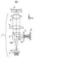
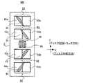
以下、本発明の実施例につき図面を参照しながら説明する。図1は本発明における光ピックアップ装置の光学系構成の一例を示した概略部品配置図である。光ピックアップ1内には、例えばDVDの記録または再生用として波長650〜660nm帯のレーザ光束を出射する半導体レーザ素子10を収納したレーザ光源2が配置されている。
Hereinafter, embodiments of the present invention will be described with reference to the drawings. FIG. 1 is a schematic component arrangement diagram showing an example of an optical system configuration of an optical pickup device according to the present invention. In the optical pickup 1, for example, a
このレーザ光源2を発した光束100は、ビームスプリッタ3を経てカップリングレンズ4に達し、このカップリングレンズ4によって略平行な光束に変換されたのち対物レンズ5に達する。そしてこの対物レンズ5により集光され、DVDなど所定の光ディスク6の記録トラック上に照射され光スポットを形成する。そして、この光ディスク6を反射した光束は、入射光束と逆の光路を辿り再び対物レンズ5、カップリングレンズ4を経てビームスプリッタ3に達し、少なくともその一部の光量に相当する光束がこのビームスプリッタ3を反射した後、信号検出用の復路光束101となって光導波素子7に達する。
The
この光導波素子7は本実施例の主要部品であり、例えば回折格子等のようにこの素子に入射した光束を所定の方向に回折する機能備えている。またこの光導波素子7は、後述するように、所定の分割線により2個の領域に分割されており、この各分割領域に入射した光束101をそれぞれ互いに異なる回折角にて回折し、光検出器8上に配置された互いに異なる所定の受光面に導く機能を備えている。
The
なお、前記した図1の実施例の光学系では、レーザ光源2を発し対物レンズ5を経てディスク6に入射する往路光束100はビームスプリッタ3を透過し、ディスク6に反射したのち光導波素子7を経て光検出器8上の所定の受光面に達する復路光束101は前記ビームスプリッタ3を反射する光学系構成となっている。しかし、当然のことながらこれとは逆に、前記往路光束100がビームスプリッタ3を反射し、前記復路光束101が前記ビームスプリッタ3を透過する構成でも一向に構わない。またビームスプリッタ3は図1に示したような四角形プリズムに限定されるものではなく、例えば斜めに傾斜して配置された平板のハーフミラー等でも構わない。
In the optical system of the embodiment of FIG. 1 described above, the
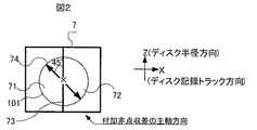
次に前記光導波素子7と光検出器8に関する具体的な実施例について述べる。図2は光導波素子7の概略構成を示す概略平面図である。この光導波素子7は透明平板の基板面上に所定の格子溝を設けた回折格子になっている。また、この光導波素子7は該格子面上においてディスク6の記録トラック方向に略垂直な方向すなわちディスク半径方向に相当する方向(図2の例ではZ軸方向)に対し略平行に伸び、かつ復路光束101の中心光軸(図中に×印にて表示)上もしくはその近傍に配置された分割線73によって領域71および72の2個の領域に分割されている。そしてこの両分割領域には、共に入射した復路光束101を前記分割線73に略平行な方向すなわち図のZ軸方向に略平行な方向に回折するように格子溝が設けられている。
Next, specific examples relating to the
ただし、前記両分割領域内での平格子溝のピッチは互いに異なっており、前記したように各分割領域に入射した復路光束101をそれぞれ異なる回折角で回折し、光検出器8上に配置された互いに異なる受光面に導くようになっている。しかも前記両分割領域は、該分割領域で回折された±1次回折光束に対して共に図のX軸およびZ軸に対して略45度に傾いた所定の方向74を主軸とする所定量の非点収差が付加されるようその配置パターンが最適設計され、不等間隔でかつ曲線状の格子溝パターンを備えたいわゆるホログラフィック回折格子になっている。
However, the pitches of the flat lattice grooves in the two divided regions are different from each other. As described above, the
このため、この光導波素子7に入射した復路光束101からは回折作用によって新たに+1次回折光束と−1次回折光束が発生するが、例えば図3(a)に示すように、このうち分割領域71に入射した復路光束101からは、±1次回折光束として光束102および103が生じ、それぞれ光検出器8内に配置された複数の受光面のうち2分割受光面82および83に入射して各受光面上で光スポット92および93を形成する。一方、分割領域72に入射した復路光束101からは、図3(b)に示すように±1次回折光束として光束104および105が生じ、前記回折光束102および103と同様に光検出器8内に配置された2分割受光面84および85に入射して各受光面上で光スポット94および95を形成する。
For this reason, a + 1st-order diffracted light beam and a −1st-order diffracted light beam are newly generated from the
ただし、図3(a)および(b)に示した例では、分割領域72での±1次回折光束の回折角が分割領域71での回折角よりも大きくなるように両分割領域での平均格子溝ピッチが設定されているため、前記回折光束104、105が入射する2分割受光面84および85は、それぞれ前記回折光束102、103が入射する2分割受光面82および83よりもさらに復路光束101の中心光軸から離れた位置に配置されている。
However, in the example shown in FIGS. 3A and 3B, the average in both divided regions is such that the diffraction angle of the ± first-order diffracted light beam in the divided
また復路光束101からは前記光導波素子7をそのまま透過する0次光束106も生じるが、この光束は図3(a)(b)に示すように光検出器8内に配置された受光面86上に集光されて光スポット96を形成する。
Further, a zero-order light beam 106 that passes through the
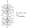
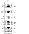
図4乃至図6は、本発明における光検出器8内の受光面の配置状態とそこに照射される前記光スポット92乃至96の集光状態を示した概略平面図である。このうち図4は光ディスク上の光スポットがジャストフォーカスの状態にある場合を示しており、図5はこのディスク上光スポットが所定の向き(例えば対物レンズとディスクの間隔が広がる向き)に所定量デフォーカスした場合、図6は図5とは反対の向きに所定量デフォーカスした場合を示している。 4 to 6 are schematic plan views showing the arrangement state of the light receiving surface in the photodetector 8 according to the present invention and the condensing state of the light spots 92 to 96 irradiated thereto. 4 shows a case where the light spot on the optical disk is in a just-focus state, and FIG. 5 shows a predetermined amount of the light spot on the disk in a predetermined direction (for example, a direction in which the distance between the objective lens and the disk widens). In the case of defocusing, FIG. 6 shows a case where a predetermined amount is defocused in the opposite direction to FIG.
各図が示すように、光検出器8内において受光面82乃至86は図のZ軸方向すなわち前記光導波素子7に設けた分割線に平行な方向にほぼ一直線状に配置されている。また前記+1次回折光束の集光スポット92および94が照射されている受光面82および84と、前記−1次回折光束の集光スポット93および95が照射されている受光面83および85は、前記0次光束の集光スポットが照射されている受光面86を中心としてそれぞれ対称な位置に配置されている。さらにこれら受光面82乃至85は、やはりZ軸方向すなわち前記光導波素子7に設けた分割線73に略平行に伸びた分割線によって各々2分割され、それぞれ独立した2個の受光領域すなわち82aと82b、83aと83b、84aと84b、そして85aと85bを形成している。そしてこれら分割受光領域の中央部すなわち各分割線の真上に前記集光スポット92乃至95がそれぞれ照射されている。
As shown in the drawings, in the photodetector 8, the light receiving surfaces 82 to 86 are arranged in a substantially straight line in the Z-axis direction in the drawing, that is, in a direction parallel to the dividing line provided in the
この時、図4のように光ディスク上の集光スポットがジャストフォーカスの状態にある場合は、集光スポット92乃至95はそれぞれ略半円形の形状になっている。しかも前記光導波素子7のホログラフィック回折格子によって付加された45度方向の非点収差の影響により、ちょうど光導波素子7の前記各分割領域71および72に入射する復路光束101の断面形状が光軸回りに略90度回転したようなスポット形状になっている。したがって、集光スポット92乃至95にとっては図のX軸方向がディスクの半径方向に相当することになる。
At this time, when the focused spot on the optical disc is in a just-focused state as shown in FIG. 4, the
しかもこの際、集光スポット92と93および94と95は、それぞれ同じ光束の+1次回折光と−1次回折光の関係であるためにその位相(波面)が共役関係にあり、その結果付加される非点収差の主軸方向が互いに90度傾斜している。このため、例えば集光スポット92と94が図面上において時計回りに90度回転した集光スポット形状になっている場合、集光スポット93と95は反時計回りに90度回転した形状になっている。つまり、集光スポット92と93および94と95は相対的に180度回転し、互いに左右が反転したスポット形状になっている。以上のような集光スポットの配置および形状になっているため、図4の状態では、例えば受光領域82aと82b、83aと83b、84aと84b、そして85aと85bのそれぞれで検出される集光スポット92乃至95の検出光量はほぼ均等になる。
In addition, at this time, since the condensing
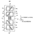
一方、図5や図6のように、ディスク上集光スポットが所定の向きにデフォーカスした場合は、前記集光スポット92乃至95は図4に示したような半円形の形状から大きな歪みが生じ、図中に示すように各受光面の分割線に対して斜め45度方向に大きく伸びたような形状になっている。このため例えば図5の例では、受光面82内の受光領域82aの方が82bより検出光量が大きくなり、全く同様に受光面83内の受光領域83aの方が83bよりも検出光量が大きくなる。
On the other hand, as shown in FIGS. 5 and 6, when the focused spot on the disc is defocused in a predetermined direction, the
一方、受光面84内では受光領域84bの方が84aよりも検出光量が大きくなり、受光面85内の受光領域85bの方が83aよりも検出光量が大きくなる。
On the other hand, in the
これに対して、図5の場合とは反対向きにデフォーカスした図6の例では、図5と例と同様に各集光スポットは各受光面の分割線に対して斜め45度方向に大きく伸びるが、その伸びる向きは、図5の場合に対して各受光面の分割線に対して対称な向きになる。このため図6の場合は、図5の場合とは反対に受光領域82b、83b、84a、85aの方が、82a、83a、84b、85bよりも検出光量が大きくなる。
On the other hand, in the example of FIG. 6 defocused in the opposite direction to the case of FIG. 5, each focused spot is large in the direction of 45 degrees obliquely with respect to the dividing line of each light receiving surface as in FIG. Although extending, the extending direction is symmetric with respect to the dividing line of each light receiving surface with respect to the case of FIG. Therefore, in the case of FIG. 6, in contrast to the case of FIG. 5, the
以上述べたような受光面上での各集光スポット形状の変化とそれに伴う各分割受光領域での検出光量変化の特性を利用して、所定の演算によりFESやTESを検出するための回路構成を図7に示す。前記分割受光領域82aおよび82b乃至85aないし85bから検出された光量検出電流は、ぞれぞれ電流−電圧変換器302a乃至305bによってぞれぞれ独立に信号電圧に変換される。今、これらの信号電圧を図中に示すようにS2a乃至S5bで表す。
A circuit configuration for detecting FES and TES by a predetermined calculation using the characteristics of the shape of each condensing spot on the light receiving surface as described above and the characteristics of the detected light amount change in each divided light receiving area. Is shown in FIG. The light amount detection currents detected from the divided
これら各信号電圧は、図中に示すように加算器401乃至404および減算器501および502によって演算処理され、FESやTESが検出される。
Each of these signal voltages is arithmetically processed by
すなわち、FESは以下の演算式から検出することができる。

なお、上記(数1)に示すような演算処理によってFESを検出する手法は,基本的には所謂非点収差方式によるFES検出とほぼ同様の光学的特性を利用した手法と見なすことができる。したがって本実施例におけるFES検出原理の詳細な説明は省略する。 It should be noted that the method of detecting FES by the arithmetic processing as shown in (Equation 1) can basically be regarded as a method using optical characteristics substantially similar to the FES detection by the so-called astigmatism method. Therefore, a detailed description of the FES detection principle in this embodiment is omitted.
一方、前記したように、集光スポット92乃至95にとっては図のX方向がディスクの半径方向に相当することになり、かつまた集光スポット92と93および94と95は相対互いに左右が反転したスポット形状になっている点を考えると、TESは以下の演算式から検出することができる。
なお、上記(数2)に示すような演算処理によってTESを検出する手法は,基本的には所謂プッシュプル方式によるTES検出とほぼ同様の光学的特性を利用した手法と見なすことができる。したがって本実施例におけるTES検出原理の詳細な説明は省略する。 It should be noted that the technique for detecting TES by the arithmetic processing shown in the above (Equation 2) can be basically regarded as a technique using optical characteristics almost the same as the TES detection by the so-called push-pull method. Therefore, a detailed description of the TES detection principle in this embodiment is omitted.
また本実施例では、ディスク上に照射された1個の光スポットの反射光からいわゆるプッシュプル方式と同等の演算処理によってTESを検出しているが、もちろん他の検出手段を用いても一向に構わない。例えば図1に示したような光学系構成において、レーザ光源2とビームスプリッタ3間の光路中に往路光束100を3本の光束に分割する回折格子を配置し、光ディスク上に3個の光スポットを照射させ、その各々から前記光学手段および演算手段によってTESを検出させ、それらを減算処理することで対物レンズのトラッキング変位に伴うTESのオフセットを良好に除去あるいは低減する所謂ディファレンシャル・プッシュプル方式を用いることも可能である。
In the present embodiment, TES is detected from the reflected light of one light spot irradiated on the disk by a calculation process equivalent to the so-called push-pull method. Of course, other detection means may be used. Absent. For example, in the optical system configuration shown in FIG. 1, a diffraction grating that divides the
以上述べたような、本発明の光学的手段や演算手段を用いることにより、光検出器等の光ピックアップをする構成光学部品の位置ずれなどの誤差要因や経時変化に対し、極めて安定した信号品質でFESやTESを検出することができる。例えば、図8は光検出器受光面のX方向位置ずれ量に対するFES振幅の相対変化の一例を表したグラフである。本発明によって検出されたFESと比較検証のために従来の非点収差方式によって検出されたFESについてプロットしている。なおどちらも受光面上の集光スポット径は約60μmで統一している。図から明らかなように、本発明によって検出されたFESの方が光検出器受光面の位置ずれに伴う振幅低下が小さく、より良好な信号が得られていることが分かる。 By using the optical means and arithmetic means of the present invention as described above, extremely stable signal quality against error factors such as positional deviation of optical components such as photodetectors, and changes over time. Can detect FES and TES. For example, FIG. 8 is a graph showing an example of the relative change in the FES amplitude with respect to the X-direction positional deviation amount of the light receiving surface of the photodetector. Plots are made for the FES detected by the present invention and the FES detected by the conventional astigmatism method for comparison verification. In both cases, the condensing spot diameter on the light receiving surface is uniform at about 60 μm. As is apparent from the figure, it can be seen that the FES detected by the present invention has a smaller amplitude drop due to the displacement of the light receiving surface of the photodetector, and a better signal is obtained.
次に、図9は光検出器受光面のX方向位置ずれ量に対するTESのオフセット変化の一例を表したグラフである。このグラフにも図8と同様、本発明との比較検証を行うため従来のプッシュプル方式で検出されたFESも併せてプロットしている。 Next, FIG. 9 is a graph showing an example of a change in TES offset with respect to the amount of positional deviation in the X direction of the light receiving surface of the photodetector. Similarly to FIG. 8, this graph also plots the FES detected by the conventional push-pull method for comparison with the present invention.
図から明らかなように、従来のプッシュプル方式では受光面の位置ずれに対し、TESにはほぼ比例的にオフセットが発生しているのに対して、本発明でのTESでは受光面が位置ずれしてもオフセットはほとんど発生せず、明らかに従来方式より良好な特性になっていることがわかる。 As is apparent from the figure, the offset is generated in the TES almost in proportion to the positional deviation of the light receiving surface in the conventional push-pull method, whereas the light receiving surface is displaced in the TES of the present invention. Even with this, almost no offset occurs, and it can be clearly seen that the characteristics are better than those of the conventional method.
このように本発明によれば、光検出器受光面が位置ずれしてもFESやTESのほとんどオフセットは発生せず、振幅低下も従来方式より良好に抑えられている。これは前記したように集光スポット92と93および94と95が互いに±1次回折光の位相共役関係にあって、ジャストフォーカス時やデフォーカス時のスポットパターンが受光面の分割線に対して互いに対称に反転した関係になっているため、一方の集光スポットから検出される信号の劣化を他方の集光スポットが自動的に補償するためである。
As described above, according to the present invention, even if the light receiving surface of the photodetector is displaced, almost no offset of FES or TES is generated, and the decrease in amplitude is suppressed better than the conventional method. As described above, the converging
なお、図8および図9では、一例として光検出器受光面のX方向位置ずれを取り上げて信号特性の変化を示したが、他の誤差要因に対しても本発明FESやTESを良好に保つことができる。例えば、光検出器受光面のZ方向(X方向に対して垂直な方向)の位置ずれについては、受光領域分割線の伸びる方向に平行な位置ずれなので、当然のことながら各集光スポットが受光面をはみ出さない限り信号品質の劣化は一切ない。またレーザ光源から発した光束の波長が変化すると、光導波素子内のホログラフィック回折格子で回折される±1次回折光の回折角が変化するという問題があるが、この場合もこの回折角の変化によって生じる集光スポットの相対位置ずれは、やはり受光領域分割線の伸びる方向に平行な位置ずれなので、当然のことながら各集光スポットが受光面をはみ出さない限り信号品質の劣化は一切ない。 8 and 9 show changes in the signal characteristics by taking the X-direction positional deviation of the light receiving surface of the photodetector as an example. However, the FES and TES of the present invention are kept good against other error factors. be able to. For example, the positional deviation in the Z direction (perpendicular to the X direction) of the light receiving surface of the photodetector is a positional deviation parallel to the direction in which the light receiving area dividing line extends. As long as the surface does not protrude, there is no signal quality degradation. Further, when the wavelength of the light beam emitted from the laser light source changes, there is a problem that the diffraction angle of ± first-order diffracted light diffracted by the holographic diffraction grating in the optical waveguide element changes. The relative positional shift of the focused spot caused by the above is also a positional shift parallel to the direction in which the light receiving area dividing line extends. Therefore, as a matter of course, there is no deterioration in signal quality unless each focused spot protrudes from the light receiving surface.
次に、実施例2として、波長の異なる2個以上のレーザ光源を同一のパッケージの中に収納したマルチレーザ光源を用いて、1個の光ピックアップ装置でDVDやCDなど異なるディスク媒体への記録または再生を実現させた互換光ピックアップ装置の実施例を示す。図10は、本実施例における光ピックアップ装置の光学系構成の一例を示した概略部品配置図である。 Next, as Example 2, using a multi-laser light source in which two or more laser light sources having different wavelengths are housed in the same package, recording on different disk media such as a DVD and a CD with one optical pickup device. Alternatively, an embodiment of a compatible optical pickup device that realizes reproduction will be described. FIG. 10 is a schematic component arrangement diagram showing an example of the optical system configuration of the optical pickup device in the present embodiment.
光ピックアップ11内には、例えばDVDの記録または再生用として波長650〜660nm帯のレーザ光束を出射する半導体レーザ素子10に加えて、CDの記録または再生用として波長780nmのレーザ光束を出射する半導体レーザ12を収納したレーザ光源2が配置されている。このレーザ光源12を発した光束107は、レーザ光源2を発した光束100と同様、ビームスプリッタ3を経てカップリングレンズ4に達し、このカップリングレンズ4によって略平行な光束に変換されたのち対物レンズ5に達する。そしてこの対物レンズ5により集光され、CDなど所定の光ディスク6の記録トラック上に照射され光スポットを形成する。そして、この光ディスク6を反射した光束は、入射光束と逆の光路を辿り再び対物レンズ5、カップリングレンズ4を経てビームスプリッタ3に達し、少なくともその一部の光量に相当する光束がこのビームスプリッタ3を反射した後、信号検出用の復路光束108となって光導波素子13に達する。
In the
図11は光導波素子13の概略構成を示す概略平面図である。本実施例における光導波素子13は、この素子に入射した波長650〜660nm帯のレーザ光束である復路光束101を所定の方向に回折させるだけでなく、この素子に入射した波長780nm帯のレーザ光束である復路光束108も回折させる点で光導波素子7と異なるが、基本的には図2の光導波素子7と同様の構成である。
FIG. 11 is a schematic plan view showing a schematic configuration of the
図12は、第2の実施例における光検出器受光面の構成とそこに照射される光スポットの集光状態の一例を示した光ピックアップ装置主要部の概略平面図である。 FIG. 12 is a schematic plan view of the main part of the optical pickup device showing an example of the configuration of the light receiving surface of the photodetector and the condensing state of the light spot irradiated thereon in the second embodiment.
この光導波素子13に入射した復路光束108からは回折作用によって新たに+1次回折光束と−1次回折光束が発生するが、このうち分割領域71に入射した復路光束108から±1次回折光束が生じて、それぞれ光検出器14内に配置された複数の受光面のうち2分割受光面82’および83に入射して各受光面上で光スポット111および112を形成する。
A + 1st order diffracted light beam and a −1st order diffracted light beam are newly generated by the diffraction action from the
一方、分割領域72に入射した復路光束108から±1次回折光束が生じて、光検出器14内に配置された2分割受光面84’および85に入射して各受光面上で光スポット113および114を形成する。ここで、92〜96は実施例1と同様、波長650nm〜660nm帯のレーザ光束の光スポットである。
On the other hand, a ± 1st-order diffracted light beam is generated from the
ただし、実施例1と同様、分割領域72での±1次回折光束の回折角が分割領域71での回折角よりも大きくなるように両分割領域での平均格子溝ピッチが設定されているため、分割領域72による回折光束が入射する2分割受光面84’および85は、分割領域71による回折光束が入射する2分割受光面82’および83よりもさらに復路光束108の中心光軸から離れた位置に配置されている。また復路光束108からは前記光導波素子13をそのまま透過する0次光束も生じ、光検出器14内に配置された受光面86上に集光されて光スポット115を形成する。
However, as in the first embodiment, the average grating groove pitch in both divided regions is set so that the diffraction angle of the ± first-order diffracted light beam in the divided
本実施例においては、波長650〜660nm帯のレーザ光束を出射するレーザ素子10と波長780nmのレーザ光束を出射するレーザ素子12はY軸方向に並んで配置されている。そのため、それぞれの光束が入射する回折格子上の位置は、図11に示したように、ディスク半径方向(Z軸方向)に所定の距離離れた位置となる。例えば0次光束が集光された光スポット115は、光スポット96と所定の距離離れた位置に形成される。
In this embodiment, the
光検出器14内において受光面82乃至85は、実施例1と同様に、図のZ軸方向すなわち前記光導波素子14に設けた分割線に平行な方向にほぼ一直線状に配置されている。また前記+1次回折光束の集光スポット111および113と、前記−1次回折光束の集光スポット112および114は、前記0次光束の集光スポット115を中心としてそれぞれ略対称な位置に形成される。
In the
さらにこれら受光面82乃至85は、やはりZ軸方向すなわち前記光導波素子14に設けた分割線73に略平行に伸びた分割線によって各々2分割され、それぞれ独立した2個の受光領域すなわち82aと82b、82’aと82’b、83aと83b、84aと84b、84’aと84’b、そして85aと85bを形成している。これら分割受光領域の各分割線の真上に前記集光スポット92乃至96、111乃至115がそれぞれ照射されている。
Furthermore, these light receiving surfaces 82 to 85 are each divided into two by a dividing line extending substantially parallel to the Z-axis direction, that is, the dividing
ここで、回折格子による回折角は波長に比例するため、650〜660nm帯の波長の回折角に対して780nm帯の波長の回折角は大きくなり、0次光束による光スポットから±1次回折光による光スポットまでの距離は650〜660nm帯の場合よりも780nm帯の場合の方が大きくなる。例えば、光スポット115から光スポット114までの距離は、光スポット96から光スポット95までの距離よりも大きく、光スポット115から光スポット113までの距離は、光スポット96から光スポット94までの距離よりも大きい。
Here, since the diffraction angle by the diffraction grating is proportional to the wavelength, the diffraction angle of the wavelength of the 780 nm band is larger than the diffraction angle of the wavelength of the 650 to 660 nm band. The distance to the light spot is larger in the 780 nm band than in the 650 to 660 nm band. For example, the distance from the
図12を用いて、光スポット115が光スポット86よりも+1次回折光側に形成されるようにレーザ素子10とレーザ素子12が設置されている場合について説明する。この場合、+1次回折光側では、回折格子の領域71と領域72の格子溝ピッチが異なることに起因する光スポット形成位置のずれと、レーザ素子10とレーザ素子12とが所定の距離をもって配置されていることに起因する光スポット形成位置のずれとが同じ方向となって重畳されるため、光スポット93と光スポット112の形成位置、及び光スポット95と光スポット114との形成位置は比較的遠くなる。対して−1次回折光側では、回折格子の領域71と領域72の格子溝ピッチが異なることに起因する光スポット形成位置のずれと、レーザ素子10とレーザ素子12とが所定の距離をもって配置されていることに起因する光スポット形成位置のずれとが逆方向となり相殺されるため、光スポット92と光スポット111の形成位置、及び光スポット94と光スポット113との形成位置は比較的近くなる。このため、−1次回折光側では受光面を共通化することができる。例えば図12では、光スポット92と光スポット111を受光する受光面は受光面82に共通化し、光スポット94と光スポット113を受光する受光面は受光面84に共通化している。これにより、受光面の数を削減することができる。以上述べた他にも変更を加えた実施例を考えられるが、いずれも本発明の範疇にある。
The case where the
1:光ピックアップ
2:レーザ光源
5:応対物レンズ
6:光ディスク
7,13:光導波素子
8:光検出器
82〜86:受光面
1: Optical pickup 2: Laser light source 5: Adaptive objective lens 6:
Claims (8)
該レーザ光源を出射したレーザ光束を集光して光学的情報記録媒体の情報記録面上に集光スポットを照射する対物レンズとを有し、
前記光学的情報記録媒体に対して前記レーザ光束を照射して前記光学的情報記録媒体に記録された情報信号を再生または前記光学的情報記録媒体に所定の情報信号を記録する光ピックアップであって、
前記集光スポットの前記情報記録面からの反射レーザ光束が入射され該レーザ光束から0次光束と±1次回折光束を回折、出射する光導波素子と、
前記光導波素子から出射された前記レーザ光束の0次光束または±1次回折光束が入射され受光した光量に応じた光検出信号を出力する複数の受光面を有する光検出器とを備え、
前記光導波素子は、該光導波素子上において前記光学的情報記録媒体の記録トラック方向に相当する方向に対して略垂直な分割線により少なくとも2個に分割された分割領域を有し、該分割領域により前記レーザ光束の0次光束、+1次回折光束、−1次回折光束を前記光検出器内で互いに異なる所定の受光面に入射させ、かつ前記+1次回折光束および前記−1次回折光束に前記記録トラック方向または前記分割線に対して光軸回りに略45度回転した方向を主軸とする所定量の非点収差を付加することを特徴とする光ピックアップ。 A laser light source;
An objective lens that focuses the laser beam emitted from the laser light source and irradiates a focused spot on the information recording surface of the optical information recording medium;
An optical pickup that irradiates the optical information recording medium with the laser beam to reproduce an information signal recorded on the optical information recording medium or record a predetermined information signal on the optical information recording medium. ,
An optical waveguide element that receives a reflected laser beam from the information recording surface of the focused spot and diffracts and emits a zero-order beam and a ± first-order diffracted beam from the laser beam;
A photodetector having a plurality of light receiving surfaces for outputting a light detection signal corresponding to the amount of light received by receiving the 0th order light beam or the ± 1st order diffracted light beam of the laser light beam emitted from the optical waveguide element;
The optical waveguide element has at least two divided areas on the optical waveguide element by a dividing line substantially perpendicular to a direction corresponding to a recording track direction of the optical information recording medium. Depending on the region, the 0th-order light beam, the + 1st-order diffracted light beam, and the −1st-order diffracted light beam are incident on different predetermined light receiving surfaces in the photodetector, and the + 1st-order diffracted light beam and the −1st-order diffracted light beam An optical pickup characterized by adding a predetermined amount of astigmatism with the main axis in the recording track direction or a direction rotated about 45 degrees around the optical axis with respect to the dividing line.
前記分割線は、少なくとも前記光導波素子に入射されるレーザ光束の略中心光軸上に配置されていることを特徴とする光ピックアップ。 The optical pickup according to claim 1,
The optical pickup according to claim 1, wherein the parting line is disposed at least on a substantially central optical axis of a laser beam incident on the optical waveguide element.
前記光導波素子は、前記分割線により分割された分割領域毎に回折、出射させた+1次回折光束および−1次回折光束の回折方向が、共に前記記録トラック方向に対して略垂直な方向または前記分割線に対して略平行な方向であることを特徴とする光ピックアップ。 An optical pickup according to claim 1 or 2,
In the optical waveguide element, the diffraction directions of the + 1st order diffracted light beam and the −1st order diffracted light beam diffracted and emitted for each divided region divided by the dividing line are both substantially perpendicular to the recording track direction or An optical pickup having a direction substantially parallel to the dividing line.
前記光導波素子は、前記分割線により分割された分割領域毎に互いに異なる平均格子溝ピッチを備えていることを特徴とする光ピックアップ。 An optical pickup according to any one of claims 1 to 3,
2. The optical pickup according to claim 1, wherein the optical waveguide element has different average grating groove pitches for each of the divided regions divided by the dividing line.
前記光導波素子は、不等間隔でかつ曲線状の格子溝パターンが形成されたホログラフィック回折格子であることを特徴とする光ピックアップ。 An optical pickup according to any one of claims 1 to 4,
2. The optical pickup according to claim 1, wherein the optical waveguide element is a holographic diffraction grating in which a curved grating groove pattern is formed at irregular intervals.
前記レーザ光束の+1次回折光束および−1次回折光束が入射する前記複数の受光面は、各々少なくとも2個の独立した受光面に分割されていることを特徴とする光ピックアップ。 An optical pickup according to any one of claims 1 to 5,
The optical pickup, wherein the plurality of light receiving surfaces on which the + 1st order diffracted light beam and the −1st order diffracted light beam of the laser light beam are incident are divided into at least two independent light receiving surfaces.
前記レーザ光束の+1次回折光束および−1次回折光束が入射する前記複数の受光面から得た前記光検出信号からフォーカス制御信号とトラッキング制御信号の双方を生成することを特徴とする光ピックアップ。 An optical pickup according to any one of claims 1 to 6,
An optical pickup characterized in that both a focus control signal and a tracking control signal are generated from the light detection signals obtained from the plurality of light receiving surfaces on which the + 1st order diffracted light beam and -1st order diffracted light beam of the laser light beam are incident.
前記光検出器は、該光検出器の内部に前記フォーカス制御信号および前記トラッキング制御信号の双方を生成するための演算部を備えたことを特徴とする光情報記録再生装置。 An optical information recording / reproducing apparatus comprising the optical pickup according to claim 7,
The optical detector includes an arithmetic unit for generating both the focus control signal and the tracking control signal inside the optical detector.
Priority Applications (1)
| Application Number | Priority Date | Filing Date | Title |
|---|---|---|---|
| JP2010259663A JP2012113767A (en) | 2010-11-22 | 2010-11-22 | Optical pickup device and optical information recording and reproducing device having the same |
Applications Claiming Priority (1)
| Application Number | Priority Date | Filing Date | Title |
|---|---|---|---|
| JP2010259663A JP2012113767A (en) | 2010-11-22 | 2010-11-22 | Optical pickup device and optical information recording and reproducing device having the same |
Publications (1)
| Publication Number | Publication Date |
|---|---|
| JP2012113767A true JP2012113767A (en) | 2012-06-14 |
Family
ID=46497816
Family Applications (1)
| Application Number | Title | Priority Date | Filing Date |
|---|---|---|---|
| JP2010259663A Pending JP2012113767A (en) | 2010-11-22 | 2010-11-22 | Optical pickup device and optical information recording and reproducing device having the same |
Country Status (1)
| Country | Link |
|---|---|
| JP (1) | JP2012113767A (en) |
Cited By (2)
| Publication number | Priority date | Publication date | Assignee | Title |
|---|---|---|---|---|
| WO2017026344A1 (en) * | 2015-08-07 | 2017-02-16 | 三菱電機株式会社 | Light detection device |
| WO2024023315A1 (en) * | 2022-07-29 | 2024-02-01 | Novanta Europe Gmbh | Detection assembly, measuring assembly, and method for determining the spatial position of a laser beam |
-
2010
- 2010-11-22 JP JP2010259663A patent/JP2012113767A/en active Pending
Cited By (3)
| Publication number | Priority date | Publication date | Assignee | Title |
|---|---|---|---|---|
| WO2017026344A1 (en) * | 2015-08-07 | 2017-02-16 | 三菱電機株式会社 | Light detection device |
| JPWO2017026344A1 (en) * | 2015-08-07 | 2018-04-12 | 三菱電機株式会社 | Photodetector |
| WO2024023315A1 (en) * | 2022-07-29 | 2024-02-01 | Novanta Europe Gmbh | Detection assembly, measuring assembly, and method for determining the spatial position of a laser beam |
Similar Documents
| Publication | Publication Date | Title |
|---|---|---|
| JP5255961B2 (en) | Optical pickup device and optical disk device | |
| JP2009170060A (en) | Optical pickup device and optical disk device | |
| US8054731B2 (en) | Photodetector and optical pickup apparatus | |
| JP2008027563A (en) | Optical pickup device | |
| US7064900B2 (en) | Optical pickup device and optical disk device and optical device and composite optical element | |
| JPH05307759A (en) | Optical pickup | |
| JP2004310840A (en) | Optical pickup | |
| JP4729418B2 (en) | Diffraction grating, optical pickup device, optical disk device | |
| JP2012113767A (en) | Optical pickup device and optical information recording and reproducing device having the same | |
| JP2004253111A (en) | Optical pickup device | |
| JP2003272218A (en) | Optical pickup device and optical reproducing device | |
| JP4222988B2 (en) | Optical pickup device and optical disk device | |
| JP3694206B2 (en) | Optical information recording / reproducing head device | |
| JP4170264B2 (en) | Optical pickup device and optical information recording / reproducing device | |
| JP3691274B2 (en) | Optical pickup and hologram element | |
| JP2008027565A (en) | Optical pickup | |
| JP3881956B2 (en) | Optical integrated unit and optical pickup device | |
| JP2007287278A (en) | Optical pickup device | |
| JP4190267B2 (en) | Optical information recording / reproducing head device | |
| JP4177298B2 (en) | Focus error detection device and optical pickup device including the same | |
| JP4053455B2 (en) | Optical integrated unit and optical pickup device including the same | |
| JP4018646B2 (en) | Optical pickup device | |
| JP2005100550A (en) | Optical pickup, and optical disk recording and reproducing device | |
| JP2011165290A (en) | Optical pickup device and optical recording and reproducing device equipped with the same | |
| JP2010267349A (en) | Optical head device, hologram element, optical integrated element, optical information processor, and signal detection method |
Legal Events
| Date | Code | Title | Description |
|---|---|---|---|
| RD04 | Notification of resignation of power of attorney |
Free format text: JAPANESE INTERMEDIATE CODE: A7424 Effective date: 20120521 |