JP2012108204A - Optical element, method for manufacturing optical element and electronic device - Google Patents
Optical element, method for manufacturing optical element and electronic device Download PDFInfo
- Publication number
- JP2012108204A JP2012108204A JP2010255124A JP2010255124A JP2012108204A JP 2012108204 A JP2012108204 A JP 2012108204A JP 2010255124 A JP2010255124 A JP 2010255124A JP 2010255124 A JP2010255124 A JP 2010255124A JP 2012108204 A JP2012108204 A JP 2012108204A
- Authority
- JP
- Japan
- Prior art keywords
- optical element
- refractive index
- layer
- optical
- conductive layer
- Prior art date
- Legal status (The legal status is an assumption and is not a legal conclusion. Google has not performed a legal analysis and makes no representation as to the accuracy of the status listed.)
- Withdrawn
Links
Images


Landscapes
- Projection Apparatus (AREA)
- Laminated Bodies (AREA)
- Solid State Image Pick-Up Elements (AREA)
- Optical Filters (AREA)
- Surface Treatment Of Optical Elements (AREA)
Abstract
Description
本発明は、光学素子、光学素子の製造方法、及び電子機器に関する。 The present invention relates to an optical element, a method for manufacturing the optical element, and an electronic apparatus.
プロジェクター等の映像装置、デジタルカメラ等の撮像装置、光ピックアップ等の記録・再生装置等の電子機器には、UV−IRカットフィルター膜や反射防止膜を有する光学素子が組み込まれている。
このような光学素子は、埃が付着すると、光学特性に悪影響を及ぼすため、防塵性が求められる。
防塵性を有する光学素子は、反射防止膜又はUV−IRカットフィルター膜が低屈折率層と高屈折率層とを交互に順次積層された構成を有し、最表層の低屈折率層に隣接する高屈折率層が、ITO(Indium Tin Oxide)にて形成されている。このように、最表層に隣接してITOの導電層を形成することにより、最表層の帯電性を低下させて、防塵性を向上させている(特許文献1から特許文献3まで)。
また、特許文献3の従来例では、反射防止膜として、基板側から順に、物理膜厚が71nmの酸化セリウムの層、物理膜厚が118nmの酸化シリコンの層、物理膜厚が8.1nmのITOの導電層、物理膜厚が10nmの最表層としての酸化シリコンの層が形成されている。
An optical element having a UV-IR cut filter film or an antireflection film is incorporated in an electronic apparatus such as a video apparatus such as a projector, an imaging apparatus such as a digital camera, or a recording / reproducing apparatus such as an optical pickup.
Such an optical element is required to be dustproof because it adversely affects optical characteristics when dust adheres.
The dust-proof optical element has a structure in which an antireflection film or a UV-IR cut filter film is alternately laminated with a low refractive index layer and a high refractive index layer, and is adjacent to the outermost low refractive index layer. The high refractive index layer to be formed is made of ITO (Indium Tin Oxide). Thus, by forming the ITO conductive layer adjacent to the outermost layer, the chargeability of the outermost layer is lowered and the dustproof property is improved (from
In the conventional example of
しかしながら、特許文献1から特許文献3までのような光学素子では、ITOのような光を吸収する導電性材料を用いた場合、光の透過率が低くなり、高精細化が求められる撮像装置などに適用するには光学特性が不十分であるという問題がある。
ここで、ITOによる光の吸収量を低減するために、ITOの導電層を薄くすることも考えられる。しかし、導電層の物理膜厚が小さい場合、高屈折率層として必要な光学膜厚を確保できなくなる。その結果、光の反射を良好に防止できなくなり、光の透過率が低下するという問題が生じる。
さらに、上述の特許文献3のような光学素子では、最表層及び導電層が薄いため、剥がれやすく光学特性の劣化を引き起こす虞があるという問題もある。また、特許文献3のような光学素子では、最表層及び導電層の2層のみが反射防止膜として機能しているので、光の反射を防止できる帯域が非常に狭いという問題がある。このような観点からも、特許文献3のような光学素子では、光学特性が不十分であり、高精細化が求められる撮像装置などに適用することが困難であるという問題がある。
However, in an optical element such as
Here, in order to reduce the amount of light absorbed by ITO, it is conceivable to make the ITO conductive layer thin. However, when the physical film thickness of the conductive layer is small, the optical film thickness necessary for the high refractive index layer cannot be secured. As a result, reflection of light cannot be satisfactorily prevented, resulting in a problem that light transmittance is reduced.
Furthermore, in the optical element as described in
本発明の目的は、防塵性を向上させることができ、光学特性に優れた光学素子、光学素子の製造方法、及び電子機器を提供することである。 An object of the present invention is to provide an optical element, a method for manufacturing an optical element, and an electronic apparatus that can improve dustproofness and have excellent optical characteristics.
[適用例1]
本適用例に係わる光学素子は、基板と、当該基板上に配置され、低屈折率層と高屈折率層とを交互に順にそれぞれ複数積層された光学機能膜と、を備える光学素子であって、前記光学機能膜の前記基板から最も離れた最表層は、第1低屈折率層であり、当該第1低屈折率層に隣接する第1高屈折率層は、複数層から構成され、当該複数層は前記最表層側から順に導電層と非導電層を配置して構成され、前記光学機能膜がUV−IRカットフィルター膜である場合、前記導電層の物理膜厚は60nm未満であることを特徴とする。
[Application Example 1]
An optical element according to this application example is an optical element that includes a substrate and an optical functional film that is disposed on the substrate and in which a plurality of low refractive index layers and high refractive index layers are alternately stacked. The outermost surface layer of the optical functional film that is farthest from the substrate is a first low refractive index layer, and the first high refractive index layer adjacent to the first low refractive index layer is composed of a plurality of layers, The plurality of layers are configured by sequentially arranging a conductive layer and a non-conductive layer from the outermost layer side, and when the optical functional film is a UV-IR cut filter film, the physical thickness of the conductive layer is less than 60 nm. It is characterized by.
この構成の本適用例では、最表層の第1低屈折率層側に導電層を形成するため、第1低屈折率層の電荷を導電層に移動させて、帯電性を低下させることができる。従って、光学素子の防塵性を容易に向上させることができる。
また、第1高屈折率層は、導電層と、他の高屈折率材料からなる非導電層とにより構成されているため、導電層の物理膜厚を小さくすることにより光の透過率の低下を抑制するとともに、非導電層により第1高屈折率層として必要な光学膜厚を確保できる。これにより、光の透過率を向上できる。
また、光学機能膜が反射防止膜である場合、反射防止膜は複数の低屈折率層と複数の高屈折率層とにより構成されているため、広い帯域で良好に反射を防止できる。そして、第1高屈折率層を構成する非導電層の物理膜厚を大きくすることにより、第1高屈折率層を剥がれにくくすることができる。
従って、本適用例では、防塵性を向上させることができ、光学特性に優れた光学素子を提供できる。
In this application example having this configuration, since the conductive layer is formed on the first low refractive index layer side of the outermost layer, the charge of the first low refractive index layer can be moved to the conductive layer to reduce the chargeability. . Therefore, the dustproof property of the optical element can be easily improved.
In addition, since the first high refractive index layer is composed of a conductive layer and a nonconductive layer made of another high refractive index material, the light transmittance is reduced by reducing the physical film thickness of the conductive layer. In addition, the non-conductive layer can secure the necessary optical film thickness as the first high refractive index layer. Thereby, the light transmittance can be improved.
Further, when the optical functional film is an antireflection film, the antireflection film is composed of a plurality of low refractive index layers and a plurality of high refractive index layers, so that reflection can be prevented well over a wide band. And the 1st high refractive index layer can be made hard to peel by enlarging the physical film thickness of the nonelectroconductive layer which comprises a 1st high refractive index layer.
Therefore, in this application example, the dust resistance can be improved, and an optical element having excellent optical characteristics can be provided.
[適用例2]
本適用例に係わる光学素子では、前記導電層は、前記非導電層に比べて物理膜厚が小さいことを特徴とする。
この構成の本適用例では、非導電層に比べて導電層の物理膜厚を小さくすることにより、光の吸収を抑制して、光の透過率を向上できる。
[Application Example 2]
In the optical element according to this application example, the conductive layer has a smaller physical film thickness than the non-conductive layer.
In this application example having this configuration, by reducing the physical film thickness of the conductive layer compared to the non-conductive layer, light absorption can be suppressed and light transmittance can be improved.
[適用例3]
本適用例に係わる光学素子では、前記第1低屈折率層は、前記複数の低屈折率層のうちで最も密度が小さいことを特徴とする。
この構成の本適用例では、最表層の密度を低くすることにより、層内に空隙が形成されるため、導電層への電荷移動の効率が増し、防塵性能を高めることができる。
[Application Example 3]
In the optical element according to this application example, the first low refractive index layer has the lowest density among the plurality of low refractive index layers.
In this application example having this configuration, by reducing the density of the outermost layer, voids are formed in the layer, so that the efficiency of charge transfer to the conductive layer increases and the dustproof performance can be improved.
[適用例4]
本適用例に係わる光学素子では、前記光学機能膜の表面抵抗値が、1×10⁶Ω/cm2以下であることを特徴とする。
この構成の本適用例では、表面抵抗値が1×10⁶Ω/cm2以下であるため、防塵性を向上できる。
[Application Example 4]
In the optical element according to this application example, the surface resistance value of the optical functional film is 1 × 10 6 Ω / cm 2 or less.
In this application example having this configuration, since the surface resistance value is 1 × 10 6 Ω / cm 2 or less, the dust resistance can be improved.
[適用例5]
本適用例に係わる光学素子では、前記光学機能膜が可視光領域である400nmから800nmまでの波長帯域で機能することを特徴とする。
この構成の本適用例では、可視光領域において、光学機能膜を、例えば、反射防止膜又はUV−IRカットフィルター膜として機能させることができる。
[Application Example 5]
In the optical element according to this application example, the optical functional film functions in a wavelength band from 400 nm to 800 nm which is a visible light region.
In this application example having this configuration, the optical functional film can function as, for example, an antireflection film or a UV-IR cut filter film in the visible light region.
[適用例6]
本適用例に係わる光学素子では、前記光学機能膜が反射防止膜であることを特徴とする。
この構成の本適用例では、上述した導電層及び非導電層を有するので、光学機能膜を反射防止膜として良好に機能させることができる。
[Application Example 6]
In the optical element according to this application example, the optical functional film is an antireflection film.
In this application example having this configuration, since the conductive layer and the non-conductive layer described above are included, the optical function film can function well as an antireflection film.
[適用例7]
本適用例に係わる光学素子では、前記導電層の物理膜厚は、5nmよりも大きく40nmよりも小さいことを特徴とする。
この構成の本適用例では、反射防止膜の導電層の物理膜厚を5nmよりも大きく40nmよりも小さくすることにより、さらに光の吸収を良好に抑制して、光の透過率を向上できる。
[Application Example 7]
In the optical element according to this application example, the physical film thickness of the conductive layer is larger than 5 nm and smaller than 40 nm.
In this application example having this configuration, by making the physical film thickness of the conductive layer of the antireflection film larger than 5 nm and smaller than 40 nm, light absorption can be further suppressed and light transmittance can be improved.
[適用例8]
本適用例に係わる光学素子の製造方法は、基板と、当該基板上に配置され、低屈折率層と高屈折率層とを交互に順にそれぞれ複数積層して構成される光学機能膜と、を備える光学素子を製造する光学素子の製造方法であって、前記光学機能膜の前記基板から最も離れた最表層を第1低屈折率層とし、当該第1低屈折率層に隣接する層を第1高屈折率層とし、前記低屈折率層の表面に、前記第1高屈折率層を積層する第1工程と、前記第1高屈折率層に、前記第1低屈折率層を積層する第2工程と、を実施し、前記第1工程で積層される前記第1高屈折率層は導電層と非導電層とを形成してなり、前記導電層は前記最表層側に形成され、前記光学機能膜がUV−IRカットフィルター膜である場合、前記導電層の物理膜厚が60nm未満となるように形成されることを特徴とする。
この構成の本適用例では、上述したように、防塵性を向上させることができ、光学特性に優れた光学素子の製造方法を提供できる。
[Application Example 8]
A method of manufacturing an optical element according to this application example includes: a substrate; and an optical functional film disposed on the substrate and configured by alternately laminating a plurality of low refractive index layers and high refractive index layers. An optical element manufacturing method for manufacturing an optical element comprising: an outermost surface layer of the optical functional film farthest from the substrate as a first low refractive index layer; and a layer adjacent to the first low refractive index layer as a first layer. A first step of laminating the first high refractive index layer on the surface of the low refractive index layer, and laminating the first low refractive index layer on the first high refractive index layer. The second step is performed, and the first high refractive index layer laminated in the first step forms a conductive layer and a non-conductive layer, and the conductive layer is formed on the outermost layer side, When the optical functional film is a UV-IR cut filter film, the physical film thickness of the conductive layer is less than 60 nm. Characterized in that it is urchin formed.
In this application example having this configuration, as described above, dustproofness can be improved, and a method for manufacturing an optical element having excellent optical characteristics can be provided.
[適用例9]
本適用例に係わる電子機器は、光源と、ダイクロイックプリズムと、前記光源と前記ダイクロイックプリズムとの間の光路に配置された光学素子と、を備え、前記光学素子が、適用例6又は7に記載の光学素子であることを特徴とする。
この構成の本適用例では、上述の光学素子を備えるため、防塵性を向上させることができ、光学特性に優れた電子機器を提供できる。
[Application Example 9]
An electronic apparatus according to this application example includes a light source, a dichroic prism, and an optical element disposed in an optical path between the light source and the dichroic prism, and the optical element is described in Application Example 6 or 7. It is characterized by being an optical element.
In this application example having this configuration, since the above-described optical element is provided, dust resistance can be improved, and an electronic apparatus having excellent optical characteristics can be provided.
[適用例10]
本適用例に係わる電子機器は、撮像素子と、当該撮像素子に対向配置された光学素子と、を備え、前記光学素子が、上述の光学素子であり、前記光学機能膜が、UV−IRカットフィルター膜であることを特徴とする。
この構成の本適用例では、上述の光学素子を備えるため、防塵性を向上させることができ、光学特性に優れた電子機器を提供できる。
[Application Example 10]
An electronic apparatus according to this application example includes an imaging element and an optical element disposed to face the imaging element, the optical element is the optical element described above, and the optical functional film is a UV-IR cut. It is a filter membrane.
In this application example having this configuration, since the above-described optical element is provided, dust resistance can be improved, and an electronic apparatus having excellent optical characteristics can be provided.
[適用例11]
本適用例に係わる電子機器は、光源と、対物レンズと、前記光源と前記対物レンズとの間の光路に配置された光学素子と、を備え、前記光学素子が、適用例6又は7に記載の光学素子であることを特徴とする。
この構成の本適用例では、上述の光学素子を備えるため、防塵性を向上させることができ、光学特性に優れた電子機器を提供できる。
[Application Example 11]
An electronic apparatus according to this application example includes a light source, an objective lens, and an optical element disposed in an optical path between the light source and the objective lens, and the optical element is described in Application Example 6 or 7. It is characterized by being an optical element.
In this application example having this configuration, since the above-described optical element is provided, dust resistance can be improved, and an electronic apparatus having excellent optical characteristics can be provided.
以下、本発明の実施形態について図面を参照して説明する。ここで、各実施形態において、同一の構成要素は同一符号を付して説明を省略もしくは簡略にする。
[第一実施形態]
まず、第一実施形態を図1及び図2に基づいて説明する。
第一実施形態は電子機器をプロジェクターなどの投射装置とし、その投射装置に組み込まれる光学素子を防塵ガラスとした例である。
図1はプロジェクターの概略構成図である。
図1において、プロジェクター100は、インテグレーター照明光学系110と、色分離光学系120と、リレー光学系130と、電気光学装置140と、投写レンズ150とを備えている。
インテグレーター照明光学系110は、光源111と、第1レンズアレイ112と、第2レンズアレイ113と、偏光変換素子114と、重畳レンズ115とを備えている。このインテグレーター照明光学系110は、電気光学装置140を構成する3枚の透過型液晶パネル141(赤、緑、青の色光毎にそれぞれ液晶パネル141R,141G,141Bとする)の画像形成領域をほぼ均一に照明する。
Embodiments of the present invention will be described below with reference to the drawings. Here, in each embodiment, the same component is denoted by the same reference numeral, and description thereof is omitted or simplified.
[First embodiment]
First, a first embodiment will be described with reference to FIGS.
The first embodiment is an example in which an electronic device is a projection device such as a projector, and an optical element incorporated in the projection device is dust-proof glass.
FIG. 1 is a schematic configuration diagram of a projector.
In FIG. 1, the
The integrator illumination
色分離光学系120は、2枚のダイクロイックミラー121,122と、反射ミラー123とを備えている。この色分離光学系120は、ダイクロイックミラー121、122によりインテグレーター照明光学系110から射出された複数の部分光束を赤(R)、緑(G)、青(B)の3色の色光に分離する。
ダイクロイックミラー121及び反射ミラー123は、青色光を透過型液晶パネル141Bに導く。
ダイクロイックミラー122は、ダイクロイックミラー121を透過した赤色光と緑色光のうちで緑色光を、フィールドレンズ151を通して、透過型液晶パネル141Gに導く。
リレー光学系130は、ダイクロイックミラー122を透過した赤色光を、入射側レンズ131と、リレーレンズ133と、反射ミラー132、134とを通して、赤色光を透過型液晶パネル141Rに導く。
The color separation
The
The
The relay
電気光学装置140は、入射された光束を画像情報に応じて変調してカラー画像を形成する。この電気光学装置140は、透過型液晶パネル141R,141G,141Bと、各透過型液晶パネル141R,141G,141Bの光入射面に設けられる防塵ガラス10と、クロスダイクロイックプリズム142とを備えている。
防塵ガラス10は、光源111とクロスダイクロイックプリズム142との間の光路に配置され、クロスダイクロイックプリズム142は、色光毎に変調された光学像を合成してカラー画像を形成する。
投写レンズ150は、クロスダイクロイックプリズム142にて形成されたカラー画像を拡大して投写する。
The electro-
The dust-
The
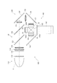
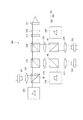
図2は、防塵ガラス10の概略構成図である。
図2において、防塵ガラス10は、基板1と、この基板1に形成された反射防止膜2とを備え、図示しないケースに収納されている。基板1は、例えば、石英、水晶、無アルカリガラス等から形成される。
この反射防止膜2は、可視光領域である400nmから800nmまでの波長帯域で機能し、低屈折率層2Aと、高屈折率層2Bとが交互に順次積層されている。基板1から最も離れた最表層2Sは、第1低屈折率層2Aである。この第1低屈折率層2Aに隣接する層は、複数層から構成された第1高屈折率層2Bである。
FIG. 2 is a schematic configuration diagram of the dust-
In FIG. 2, a
This
第1高屈折率層2Bは、最表層2S側から順に第2層としての導電層22と、第3層としての非導電層23とを有する。
第1高屈折率層2Bに隣接する第4層24は、第2低屈折率層2Aであり、第2低屈折率層2Aに隣接する第5層25は、第2高屈折率層2Bであり、第2高屈折率層2Bに隣接する第6層26は、基板1に隣接した第3低屈折率層2Aである。第1高屈折率層2Bは、2層からなるため、反射防止膜2は全体として6層からなる。なお、第1高屈折率層2Bは、3層以上からなってもよい。
この第1低屈折率層2Aは、第1低屈折率層2Aと、第2低屈折率層2Aと、第3低屈折率層2Aとのうちで最も密度が低いことが好ましい。
The first high
The
The first low
導電層22は、非導電層23に比べて物理膜厚が小さいことが好ましい。すなわち、導電層22の物理膜厚をtiとし、非導電層23の物理膜厚をthとしたとき、ti<thであることが好ましい。また、tiの厚みは、5nm<ti<40nmであることが好ましい。
低屈折率層2Aを形成する低屈折率材料としては、二酸化ケイ素(SiO2)、フッ化マグネシウム(MgF2)などが挙げられる。高屈折率層2Bを形成する高屈折率材料としては、酸化チタン(TiO2)、ITO、IWO、SnO2、酸化亜鉛(ZnO)、酸化セリウム、酸化ジルコニウム、五酸化二タンタル、五酸化二ニオブ、酸化ハフニウム(HfO2)、ランタンチタネート(混合物)などが挙げられる。これらの材料のうち導電層22を形成する導電性材料としては、ITO、IWO、SnO2、酸化亜鉛(ZnO)などが挙げられる。非導電層23を形成する非導電性材料としては、TiO2、酸化セリウム、酸化ジルコニウム、五酸化二タンタル、五酸化二ニオブ、酸化ハフニウム(HfO2)、ランタンチタネート(混合物)などが挙げられる。
なお、反射防止膜2は、第1低屈折率層2Aの基板1と反対側の表面に防塵層3を有してもよい。
反射防止膜2が防塵層3を有する場合、その反射防止膜2の表面抵抗値が1×10⁶Ω/cm2以下であることが好ましい。
防塵層3を形成する防塵性材料としては、フッ素含有有機ケイ素化合物、フッ化マグネシウムなどが挙げられる。
The
Examples of the low refractive index material for forming the low
The
When the
Examples of the dustproof material for forming the
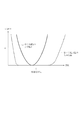
ここで、第一実施形態の防塵ガラス10と、上記特許文献3に記載された光学素子とについて、可視光領域における光の透過率を対比した結果が図3に示されている。
特許文献3の光学素子では、上述したように、反射防止膜として機能する層が1つの低屈折率層と1つの高屈折率層との2層しかないため、可視光領域のうちの狭い波長領域でしか反射を防止できない。
一方、第一実施形態の防塵ガラス10では、反射防止膜として機能する層が3つの低屈折率層2Aと2つの高屈折率層2Bとで構成されているため、可視光領域において全体的に反射を防止できる。
Here, the result of comparing the light transmittance in the visible light region for the dust-
In the optical element of
On the other hand, in the dust-
次に、防塵ガラス10を製造する方法について説明する。
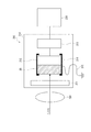
図4は、基板1に反射防止膜2を形成するための装置の概略図である。
図4において、成膜装置は、アースされた室50と、この室50の天井部分に回動自在に支持されたドーム51を備えている。
ドーム51は、その中央部に設けられた回転軸51Aを介してモーター52により回動される。ドーム51には成膜対象となる基板1が複数取り付けられており、これらの基板1に対向するように室50の下部に第一蒸着源53と第二蒸着源541と第三蒸着源542とが設けられている。第一蒸着源53にはSiO2などの低屈折率材料が収納され、第二蒸着源541には、TiO2などの高屈折率材料が収納され、第三蒸着源542には、ITOなどの導電性材料が収納されている。
第一蒸着源53と第二蒸着源541との間にはイオン源55と電子銃56とが配置されている。イオン源55はイオンを放出してアシストするものである。電子銃56は電子ビームを照射するものである。ドーム51の中央部には監視装置57が設けられている。この監視装置57は、基板1に成膜される膜厚を管理する光学モニターと、レート管理する水晶モニターとを備えている。
Next, a method for manufacturing the
FIG. 4 is a schematic view of an apparatus for forming the
In FIG. 4, the film forming apparatus includes a grounded
The
An
次に、この成膜装置を用いて基板1に6層からなる反射防止膜2を形成する方法を説明する。まず基板1がドーム51にセットされた後、ドーム51が回転しつつ、電子銃56から電子ビームが照射され、第一蒸着源53に収納されるSiO2と、第二蒸着源541に収納されるTiO2とが基板1に蒸着される。
この際、イオン源55からイオン化した酸素が加速照射されることにより、基板1の上にSiO2の第3低屈折率層2Aと、TiO2の第2高屈折率層2Bと、SiO2の第2低屈折率層2Aと、TiO2の非導電層23とが交互に積層される。
そして、非導電層23が形成された後、第三蒸着源542に収納されるITOが非導電層23に積層されて、導電層22が形成される。これにより、第1高屈折率層2Bが形成される(第1工程)。そして、導電層22にSiO2の最表層2Sが形成される(第2工程)。
ここで、最表層2S及び導電層22は、ノンアシストパワー(EB蒸着)又は300V以上500V以下の加速電圧(450mA以上600mA以下の加速電流)の低アシストパワー(IAD)で形成されることが好ましい。
一方、最表層2S及び導電層22以外の第3低屈折率層2Aと、第2高屈折率層2Bと、第2低屈折率層2Aと、非導電層23とは、700V以上1000V以下の加速電圧(800mA以上1200mA以下の加速電流)の高アシストパワー(IAD)で形成されることが好ましい。
Next, a method for forming the
At this time, the ionized oxygen from the
Then, after the
Here, the
On the other hand, the third low-
基板1に反射防止膜2が成形された後、この反射防止膜2の上に防塵層3が必要に応じて形成される。
この防塵層3が形成される際は、反射防止膜2が形成された基板1と、防塵性材料が収納された蒸着源が真空装置の内部にセットされ、減圧排気が行われる。そして、基板1の温度を60℃とした状態で蒸発源が約600℃に加熱され、防塵性材料が蒸発して反射防止膜2に防塵層3が形成される。
After the
When the
[第一実施形態の効果]
本実施形態によれば、以下の効果を奏することができる。
(1)最表層2S側に導電層22を形成するため、最表層2Sの電荷を低減でき、防塵ガラス10の防塵性を容易に向上できる。また、最表層2Sは、導電層22と、非導電層23とにより構成されているため、導電層22の物理膜厚を小さくして光の透過率の低下を抑制するとともに、非導電層23により第1高屈折率層2Bとして必要な光学膜厚を確保して光の反射を防止できる。
[Effect of the first embodiment]
According to this embodiment, the following effects can be achieved.
(1) Since the
(2)反射防止膜2が複数の低屈折率層2Aと複数の高屈折率層2Bとにより構成されているため、可視光領域である400nmから800nmまでの波長帯域において広く光の反射を防止できる。
(3)非導電層23の物理膜厚を大きくすることにより、第1高屈折率層2Bを剥がれにくくすることができる。
(4)導電層22の物理膜厚を非導電層23よりも小さくすることにより、さらに光の吸収を抑制して、光の透過率を向上できる。
(5)導電層22の物理膜厚を5nmよりも大きく40nmよりも小さくすることにより、さらに光の吸収を良好に抑制して、光の透過率を向上できる。
(6)最表層2Sを3つの低屈折率層2Aの中で最も低密度とすることにより、防塵性能を向上できる。
(7)反射防止膜2の表面抵抗値を1×10⁶Ω/cm2以下とすることにより、さらに防塵性を向上できる。
(2) Since the
(3) By increasing the physical film thickness of the
(4) By making the physical film thickness of the
(5) By making the physical film thickness of the
(6) The dustproof performance can be improved by setting the
(7) By setting the surface resistance value of the
(8)本実施形態の製造方法は、第1高屈折率層2Bとして、最表層2S側から順に導電層22と非導電層23とを形成するため、防塵性を向上させることができ、光学特性に優れた防塵ガラス10の製造方法を提供できる。
(9)プロジェクター100は、防塵ガラス10を備えるため、防塵性を向上させることができ、光学特性に優れる。
(8) Since the manufacturing method of this embodiment forms the
(9) Since the
[第二実施形態]
次に、第二実施形態を図5及び図6に基づいて説明する。
第二実施形態は電子機器をデジタルスチールカメラの撮像装置とし、その撮像装置に組み込まれる光学素子を光学多層膜フィルターとした例である。
図5は、撮像装置の概略構成図である。
図5において、撮像装置200は、撮像モジュール210と、光入射側に配置されるレンズ220と、撮像モジュール210から出力される撮像信号の記録・再生等を行う本体部230とを含んで構成されている。この本体部230には、撮像信号の補正等を行う信号処理部と、撮像信号を磁気テープ等の記録媒体に記録する記録部と、この撮像信号を再生する再生部と、再生された映像を表示する表示部などの構成要素が含まれる。
撮像モジュール210は、光学多層膜フィルター20と、光学ローパスフィルター211と、光学像を電気的に変換する撮像素子のCCD(電荷結合素子)212と、この撮像素子212を駆動する駆動部213とを含んで構成されている。
[Second Embodiment]
Next, 2nd embodiment is described based on FIG.5 and FIG.6.
The second embodiment is an example in which an electronic device is an imaging device of a digital still camera, and an optical element incorporated in the imaging device is an optical multilayer filter.
FIG. 5 is a schematic configuration diagram of the imaging apparatus.
In FIG. 5, the
The
光学多層膜フィルター20は、CCD212の前面に、ケースとしての固定治具214によってCCD212と一体的に構成されている。この光学多層膜フィルター20は、IRとUVとをカットする機能の他、CCD212の防塵ガラス機能を併せて有している。
固定治具214は金属によって構成されており、光学多層膜フィルター20と電気的に接続されている。そして、固定治具214は、アースケーブル215によってアース(地落)されている。
The
The fixing
図6は、光学多層膜フィルター20の概略構成である。
図6において、光学多層膜フィルター20は、基板1と、基板1に形成されたUV−IRカットフィルター膜4とを備えている。
UV−IRカットフィルター膜4は、可視光領域である400nmから800nmまでの波長帯域で機能し、低屈折率層2Aと、高屈折率層2Bとがそれぞれ交互に複数積層されている。UV−IRカットフィルター膜4は、最表層2Sである第1低屈折率層2Aと、第2層の導電層22と第3層の非導電層23とを構成する第1高屈折率層2Bと、第4層24である第2低屈折率層2Aと、第5層25である第2高屈折率層2Bとなどを順に備える。そして、第39層239は、第19高屈折率層2Bであり、第40層240は、基板1に隣接する第20低屈折率層2Aである。
ここで、第2層の導電層22は、その物理膜厚が60nm未満である。物理膜厚が60nm以上の場合、光の透過率が低くなる。
なお、光学多層膜フィルター20のUV−IRカットフィルター膜4は、基板1と反対側の表面に防塵層3を有していても良い。
FIG. 6 is a schematic configuration of the
In FIG. 6, the
The UV-IR cut filter film 4 functions in a wavelength band from 400 nm to 800 nm which is a visible light region, and a plurality of low refractive index layers 2A and high refractive index layers 2B are alternately stacked. The UV-IR cut filter film 4 includes a first high
Here, the second
The UV-IR cut filter film 4 of the
次に、光学多層膜フィルター20を製造する方法について説明する。
この光学多層膜フィルター20は第一実施形態の防塵ガラスと同様に図4で示される装置を用いて製造される。
まず、基板1がドーム51にセットされ、その後、ドーム51が回転しながら、電子銃56で電子ビームが照射されて第一蒸着源53のSiO2と、第二蒸着源541のTiO2とが交互に積層される。
そして、第4層の第2低屈折率層2Aが積層された後、第2低屈折率層2Aに第二蒸着源541のTiO2が蒸着され、第3層の非導電層23が形成される。
続けて、第3層の非導電層23に、第三蒸着源542のITOが蒸着され、導電層22が形成される(第1工程)。ここで、導電層22は、その物理膜厚が60nm未満となるように形成される。これにより、第1高屈折率層2Bが形成される。そして、導電層22にSiO2の最表層2Sが形成される(第2工程)。
なお、第一実施形態と同様に、最表層2S及び導電層22は、ノンアシストパワー又は低アシストパワーで形成されることが好ましく、最表層2S及び導電層22以外の層23、2A,2Bは高アシストパワーで形成されることが好ましい。
Next, a method for manufacturing the
This
First, the
Then, after the second low
Subsequently, ITO of the third
As in the first embodiment, the
第二実施形態においても、基板1に形成されたUV−IRカットフィルター膜4に必要に応じて防塵層3が設けられてもよいが、その場合は、第一実施形態と同様の方法で実施される。
第二実施形態によれば、第一実施形態と同様の効果を奏する。
Also in the second embodiment, the dust-
According to the second embodiment, there are the same effects as in the first embodiment.
[第三実施形態]
次に、第三実施形態を図7に基づいて説明する。
第三実施形態は電子機器を光ピックアップ装置とし、その光ピックアップ装置に組み込まれる光学素子をビームスプリッターとした例である。
図7は、記録再生装置の概略構成図である。
図7において、光ピックアップ300は、焦点位置の異なる3種の光記録媒体である光ディスク(CD301、DVD302、BD303)に対して互いに波長の異なる3種類のレーザービームを照射し、それぞれ所定の信号を検出するように構成されている。
具体的には、光ピックアップ300は、CD301に関する光学系として、レーザー光を発生するレーザー光源としてのレーザーダイオード310、コリメートレンズ311、偏光ビームスプリッター30、レンズ313、ダイクロイックプリズム314、1/4波長板315、開口フィルター316、対物レンズ317、及びCD301のデータピットから反射された反射レーザー光を受光し、電気信号に変換することにより前記データピットに書き込まれた信号を検出する信号検出系318を含んで構成される。
[Third embodiment]
Next, a third embodiment will be described based on FIG.
The third embodiment is an example in which an electronic apparatus is an optical pickup device, and an optical element incorporated in the optical pickup device is a beam splitter.
FIG. 7 is a schematic configuration diagram of the recording / reproducing apparatus.
In FIG. 7, an
Specifically, the
光ピックアップ300は、DVD302に関する光学系として、レーザービームを発生するレーザー光源としてのLD321、レンズ322、偏光ビームスプリッター30、及びレーザービームでDVD302のデータピットから反射された反射レーザー光を受光し、電気信号に変換することにより前記データピットに書き込まれた信号を検出する信号検出系323を含んで構成される。
光ピックアップ300は、BD303に関する光学系として、レーザービームを発生するレーザー光源としてのLD331、レンズ332、偏光ビームスプリッター30、レンズ333、ダイクロイックプリズム334及びレーザービームでBD303のデータピットから反射された反射レーザー光を受光し、電気信号に変換することにより前記データピットに書き込まれた信号を検出する信号検出系335を含んで構成される。
偏光ビームスプリッター30の概略構成は基板1の形状を除いては図2で示される防塵ガラス10と同じである。つまり、偏光ビームスプリッター30は、プリズムの入出射面に反射防止膜2が設けられ、この反射防止膜2の表面に防塵層3が必要に応じて設けられた構造である。さらに、前記プリズムに反射防止膜2が成膜され、この反射防止膜2に防塵層3が成膜される方法は第一実施形態と同じである。
前記光ディスクが搭載された部位の近くに配置された対物レンズ317、1/4波長板315、及び開口フィルター316の表面には、光ディスク(CD301、DVD302、BD303)を交換する際に、外界の塵などのほこりが前記部位から浸入し、当該塵が付着し易いので、前記表面に形成されている反射防止膜の表面に前記防塵層を配置することも有効である。
第三実施形態によれば、第一実施形態と同様の効果を奏する。
The
The
The schematic configuration of the
When the optical disk (CD301, DVD302, BD303) is exchanged on the surfaces of the
According to the third embodiment, there are the same effects as in the first embodiment.
なお、本発明は、上述した一実施形態に限定されるものではなく、本発明の目的を達成できる範囲で以下に示される変形をも含むものである。
例えば、本発明では、光学素子は前述の構成のものに限定されない。例えば、第一実施形態では、本発明の対象となる光学素子を、例えば、偏光変換素子としてもよい。さらに、第二実施形態では、本発明の対象となる光学素子を、例えば、光学ローパスフィルターとしてもよい。要するに、本発明では、基板の上に反射防止膜やUV−IRカットフィルター膜を含め光学機能膜が形成される光学素子であれば、いかなるものでも適用される。
また、第一実施形態では、光学機能膜として反射防止膜を説明し、第二実施形態では、光学機能膜としてUV−IRカットフィルター膜を説明したがこれに限られない。例えば、光学機能膜としては、UVカットフィルター膜、IRカットフィルター膜、偏光分離膜等でもよい。
Note that the present invention is not limited to the above-described embodiment, and includes the following modifications as long as the object of the present invention can be achieved.
For example, in the present invention, the optical element is not limited to the above-described configuration. For example, in the first embodiment, the optical element that is the subject of the present invention may be, for example, a polarization conversion element. Furthermore, in the second embodiment, the optical element that is the subject of the present invention may be, for example, an optical low-pass filter. In short, in the present invention, any optical element can be applied as long as an optical functional film including an antireflection film and a UV-IR cut filter film is formed on the substrate.
In the first embodiment, an antireflection film has been described as the optical function film. In the second embodiment, a UV-IR cut filter film has been described as the optical function film, but the present invention is not limited thereto. For example, the optical functional film may be a UV cut filter film, an IR cut filter film, a polarization separation film, or the like.
本実施形態の実施例について説明する。
[反射防止膜を有する光学素子]
本発明の第一実施形態の光学素子に対応する実施例1から実施例5まで、参考例1、比較例1について説明する。なお、蒸着実験では、シンクロン製蒸着機(商品名SID−1350)を用いた。また、各実験では、所定形状のサンプル、例えば、直径30mm、厚さ0.3mmの白板ガラス(屈折率n=1.51)の表面に、各実施例、参考例及び比較例に応じた条件で反射防止膜を作製した。
Examples of the present embodiment will be described.
[Optical element having antireflection film]
Reference Example 1 and Comparative Example 1 will be described from Example 1 to Example 5 corresponding to the optical element of the first embodiment of the present invention. In the vapor deposition experiment, a Shincron vapor deposition machine (trade name SID-1350) was used. Moreover, in each experiment, the conditions according to each Example, a reference example, and a comparative example on the surface of a sample of a predetermined shape, for example, a white plate glass (refractive index n = 1.51) having a diameter of 30 mm and a thickness of 0.3 mm. An antireflective film was prepared.
(実施例1)
実施例1では、基板1の上に表1のような反射防止膜を形成した。
反射防止膜の最表層2S(第1層)及び導電層(第2層)は、ノンアシストパワー(EB蒸着)で成膜した。第3層から第6層までは、高アシストパワーによるイオンアシストを用いた電子ビーム蒸着(IAD)で成膜した。この場合のアシストパワーは加速電圧が1000Vであり、加速電流が1200mAである。ここで、導電層(第2層)の物理膜厚は、5nmとなるように設定した。また、設計波長は、510nmに設定し、入射角は、0°に設定した。
Example 1
In Example 1, an antireflection film as shown in Table 1 was formed on the
The
(実施例2から実施例5まで)
実施例2から実施例5まででは、それぞれ表2から表5までに示すように、導電層の物理膜厚を10nm、20nm、40nm、60nmとした以外は、実施例1と同様にして光学素子を作製した。
(参考例1)
TiO2のみで第1高屈折率層を形成した以外は、実施例1と同様にして表6に示すように参考例1の光学素子を作製した。
(比較例1)
ITOのみで第1高屈折率層を形成した以外は、実施例1と同様にして表7に示すように比較例1の光学素子を作製した。
(Example 2 to Example 5)
In Example 2 to Example 5, as shown in Tables 2 to 5, respectively, the optical element was the same as Example 1 except that the physical film thickness of the conductive layer was 10 nm, 20 nm, 40 nm, and 60 nm. Was made.
(Reference Example 1)
An optical element of Reference Example 1 was produced as shown in Table 6 in the same manner as in Example 1 except that the first high refractive index layer was formed only with TiO 2 .
(Comparative Example 1)
An optical element of Comparative Example 1 was produced as shown in Table 7 in the same manner as Example 1 except that the first high refractive index layer was formed only from ITO.
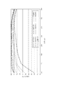
(評価方法)
実施例、参考例及び比較例の光学素子について、可視光領域での光の反射率及び透過率を測定した。その結果が図8,9に示されている。
(Evaluation methods)
About the optical element of an Example, a reference example, and a comparative example, the reflectance and transmittance | permeability of the light in visible region were measured. The results are shown in FIGS.
(実施例1) Example 1

(実施例2) (Example 2)
(実施例3) (Example 3)
(実施例4) Example 4
(実施例5) (Example 5)
(参考例1) (Reference Example 1)
(比較例1) (Comparative Example 1)
(実験結果)
(1−1)反射率
図8に示される通り、実施例1から実施例5まででは、ITOの導電層の物理膜厚を小さくし、かつ、第1高屈折率層を構成する非導電層を設けたため、反射率が小さくなることが分かった。
また、ITOのみを用いて第1高屈折率層を形成した比較例1では、ITOの導電層の物理膜厚が大きいため、反射率は比較的低かった。
一方、TiO2のみを用いて第1高屈折率層を形成した参考例1では、低波長帯域において、やや反射率が高くなり、光学特性が低下することが分かった。
(1−2)透過率
図9に示される通り、参考例1では、ITOを用いていないため、全ての可視光領域において透過率が優れていた。また、実施例1から実施例5でも同様に、ITOの導電層を小さくしたため、透過率が90%を超えて良好となることが分かった。
一方、比較例1では、特に低波長帯域において、透過率が低くなり、光学特性が低下することが分かった。
(Experimental result)
(1-1) Reflectance As shown in FIG. 8, in Examples 1 to 5, the non-conductive layer that reduces the physical film thickness of the ITO conductive layer and constitutes the first high-refractive index layer. It has been found that the reflectance is small because of the provision of.
In Comparative Example 1 in which the first high refractive index layer was formed using only ITO, the reflectivity was relatively low because the physical film thickness of the ITO conductive layer was large.
On the other hand, it was found that in Reference Example 1 in which the first high refractive index layer was formed using only TiO 2 , the reflectance was slightly increased in the low wavelength band, and the optical characteristics were lowered.
(1-2) Transmittance As shown in FIG. 9, in Reference Example 1, since ITO was not used, the transmittance was excellent in all visible light regions. Similarly, in Example 1 to Example 5, since the ITO conductive layer was made small, it was found that the transmittance exceeded 90% and became good.
On the other hand, in Comparative Example 1, it was found that the transmittance is lowered particularly in the low wavelength band, and the optical characteristics are deteriorated.
[UV−IRカットフィルター膜を有する光学素子]
本発明の第二実施形態の光学素子に対応する実施例6から実施例9まで、参考例2、比較例2,3について説明する。なお、各層の蒸着方法に関しては、上述の実施例1と同様である。
[Optical element having UV-IR cut filter film]
Reference Example 2 and Comparative Examples 2 and 3 will be described from Example 6 to Example 9 corresponding to the optical element of the second embodiment of the present invention. In addition, regarding the vapor deposition method of each layer, it is the same as that of the above-mentioned Example 1.
(実施例6)
実施例6では、基板1上に表8に示すようなUV−IRカットフィルター膜を形成した。
UV−IRカットフィルター膜の最表層2S(第1層)及び導電層(第2層)は、ノンアシストパワー(EB蒸着)で成膜した。第3層から第40層までの層は、高アシストパワーによるイオンアシストを用いた電子ビーム蒸着で成膜した。この場合のアシストパワーは加速電圧が1000Vであり、加速電流が1200mAである。ここで、導電層(第2層)の物理膜厚は、5nmとなるように設定した。また、入射角は、0°に設定した。
(Example 6)
In Example 6, a UV-IR cut filter film as shown in Table 8 was formed on the
The
(実施例7から実施例9まで)
実施例7から実施例9まででは、それぞれ表9から表11までに示すように、導電層の物理膜厚を10nm、20nm、40nmとした以外は、実施例6と同様にして光学素子を作製した。
(参考例2)
TiO2のみで第1高屈折率層を形成した以外は、表12に示すように実施例6と同様にして参考例2の光学素子を作製した。
(比較例2)
ITOのみで第1高屈折率層を形成した以外は、表13に示すように実施例6と同様にして比較例2の光学素子を作製した。
(比較例3)
導電層の物理膜厚を60nmとした以外は、表14に示すように実施例6と同様にして比較例3の光学素子を作製した。
(評価方法)
実施例及び比較例の光学素子について、紫外線領域、可視光領域、赤外線領域での光の透過率を測定した。その結果を図10,11に示す。
(Example 7 to Example 9)
In Example 7 to Example 9, as shown in Table 9 to Table 11 respectively, optical elements were produced in the same manner as Example 6 except that the physical film thickness of the conductive layer was 10 nm, 20 nm, and 40 nm. did.
(Reference Example 2)
An optical element of Reference Example 2 was produced in the same manner as in Example 6 as shown in Table 12 except that the first high refractive index layer was formed only with TiO 2 .
(Comparative Example 2)
An optical element of Comparative Example 2 was produced in the same manner as in Example 6 as shown in Table 13 except that the first high refractive index layer was formed only from ITO.
(Comparative Example 3)
An optical element of Comparative Example 3 was produced in the same manner as in Example 6 as shown in Table 14 except that the physical film thickness of the conductive layer was changed to 60 nm.
(Evaluation methods)
About the optical element of an Example and a comparative example, the transmittance | permeability of the light in an ultraviolet region, a visible light region, and an infrared region was measured. The results are shown in FIGS.
(実施例6) (Example 6)
(実施例7) (Example 7)
(実施例8) (Example 8)
(実施例9) Example 9
(参考例2) (Reference Example 2)
(比較例2) (Comparative Example 2)
(比較例3) (Comparative Example 3)
(実験結果)
(2)透過率
図10,11に示される通り、TiO2のみを用いて第1高屈折率層を形成した参考例2では、ITOを用いていないため、可視光領域において透過率が高かった。
実施例6から実施例9では、第1高屈折率層にITOの導電層を形成し、このITOの導電層の物理膜厚を60nm未満としたため、参考例1と同様に、透過率が高くなることが分かった。
一方、ITOのみを用いて第1高屈折率層を形成した比較例2と、ITOの導電層の物理膜厚を60nmとした比較例3では、透過率が低くなり、光学特性が低下することが分かった。
(Experimental result)
(2) Transmittance As shown in FIGS. 10 and 11, in Reference Example 2 in which the first high refractive index layer was formed using only TiO 2 , the transmittance was high in the visible light region because ITO was not used. .
In Example 6 to Example 9, an ITO conductive layer was formed on the first high refractive index layer, and the physical film thickness of the ITO conductive layer was less than 60 nm. Therefore, as in Reference Example 1, the transmittance was high. I found out that
On the other hand, in Comparative Example 2 in which the first high refractive index layer is formed using only ITO and Comparative Example 3 in which the physical film thickness of the ITO conductive layer is 60 nm, the transmittance is low and the optical characteristics are deteriorated. I understood.
[防塵層を有する光学素子]
(実施例10)
実施例10では、基板の上に実施例6ようなのUV−IRカットフィルター膜を設け、さらにUV−IRカットフィルター膜上にフッ素含有有機ケイ素化合物膜を形成した。
フッ素含有有機ケイ素化合物膜は、例えば、信越化学工業株式会社製フッ素含有有機ケイ素化合物(製品名KY−130)をフッ素系溶剤(住友スリーエム株式会社製:ノベックHFE−7200)で希釈して固形分濃度3%の溶液を調製し、これを多孔質セラミック製ペレットに1g含浸させ乾燥したものである。
最表層は、表15に示すようにノンアシストパワーにて成膜した。最表層以外の層は、表16に示す条件で形成した。
[Optical element with dustproof layer]
(Example 10)
In Example 10, a UV-IR cut filter film as in Example 6 was provided on a substrate, and a fluorine-containing organosilicon compound film was further formed on the UV-IR cut filter film.
The fluorine-containing organosilicon compound film is obtained by, for example, diluting a fluorine-containing organosilicon compound (product name KY-130) manufactured by Shin-Etsu Chemical Co., Ltd. with a fluorine-based solvent (manufactured by Sumitomo 3M: Novec HFE-7200). A solution having a concentration of 3% was prepared and impregnated with 1 g of porous ceramic pellets and dried.
The outermost layer was formed with non-assist power as shown in Table 15. The layers other than the outermost layer were formed under the conditions shown in Table 16.
(実施例11,12及び比較例4,5)
最表層を、表15のように、実施例11,12では低アシストパワーにて成膜し、比較例4,5では高アシストパワーにて成膜した以外は、実施例10と同様にして防塵層を有する光学素子を作製した。
(Examples 11 and 12 and Comparative Examples 4 and 5)
As shown in Table 15, the outermost layer was formed with low assist power in Examples 11 and 12, and dust-proofing was performed in the same manner as in Example 10 except that Comparative Examples 4 and 5 were formed with high assist power. An optical element having a layer was produced.
[実験結果]
各実施例、参考例、比較例について、防塵性能試験を(3−1)ポリエチレンパウダー法、(3−2)関東ローム法、(3−3)コットンリンタ法で実施した。
(3−1)ポリエチレンパウダー法
ポリエチレンパウダー法は、トレイに敷き詰めたポリエチレンパウダー(セイシン製:SK−PE−20L)の上にサンプルを1cm上から落とし、その後、ゆっくり引き上げ、サンプルに付着したパウダーの着塵量と残存量とを量るものである。着塵量はパウダーが付着したサンプルを簡単に払い、サンプルの表面を撮像し、画像解析により塵面積を計算する。残存量はパウダーがついたサンプルの表面をエアーブロー(サンプルからの距離が3cm、圧力が約50KPa、回数3回)で除塵した後、サンプルの表面を撮像し、画像解析により塵面積を計算する。
(3−2)関東ローム法
関東ローム法は、路上、野外の塵を想定してJISで規格化されたパウダー(JIS試験粉体1,7種)を試験に使用するもので、トレイに敷き詰めたパウダーにサンプルを落とし、余分な塵を落とした後、サンプルに付着したパウダーの着塵量と残存量とを量るものである。着塵量と残存量との求め方はポリエチレンパウダー法と同じである。
(3−3)コットンリンタ法
コットンリンタ法は、トレイに敷き詰められたコットンリンタと称される繊維塵を試験に使用するもので、トレイに敷き詰めたパウダーにサンプルを落とし、余分な塵を落とした後、サンプルに付着したパウダーの着塵量と残存量とを量るものである。着塵量と残存量との求め方はポリエチレンパウダー法と同じである。
[Experimental result]
About each Example, the reference example, and the comparative example, the dustproof performance test was implemented by the (3-1) polyethylene powder method, the (3-2) Kanto loam method, and the (3-3) cotton linter method.
(3-1) Polyethylene powder method In the polyethylene powder method, a sample is dropped from above 1 cm onto polyethylene powder (manufactured by Seishin: SK-PE-20L) spread on a tray, and then slowly pulled up, the powder adhered to the sample. The amount of dust and the remaining amount are measured. As for the amount of dust, the sample with powder attached is simply paid, the surface of the sample is imaged, and the dust area is calculated by image analysis. The remaining amount is to remove the dust on the surface of the sample with powder by air blow (the distance from the sample is 3 cm, the pressure is about 50 KPa, 3 times), then image the surface of the sample and calculate the dust area by image analysis .
(3-2) Kanto Loam Method The Kanto Loam method uses powders (1, 7 kinds of JIS test powders) standardized by JIS, assuming dust on the road and in the field, and spreads on a tray. The sample is dropped on the powder, excess dust is dropped, and the amount of dust attached to the sample and the remaining amount are measured. The method for obtaining the dusting amount and the residual amount is the same as that in the polyethylene powder method.
(3-3) Cotton linter method The cotton linter method uses fiber dust called cotton linter spread on a tray for the test. The sample was dropped on the powder spread on the tray, and excess dust was dropped. Thereafter, the amount of dust adhering to the sample and the remaining amount are measured. The method for obtaining the dusting amount and the residual amount is the same as that in the polyethylene powder method.
これらの方法で実施した防塵性能試験の結果を表17に示す。
表17では、(4−1)ポリエチレンパウダー法、(4−2)関東ローム法及び(4−3)コットンリンタ法の結果が示される。
表17に示される通り、ポリエチレンパウダー法、関東ローム法、コットンリンタ法の全てにおいて、実施例10から実施例12までの光学素子では比較例4,5の光学素子と比較して着塵量と残存量とがともに小さいことが分かった。
すなわち、実施例10から実施例12まででは、第1低屈折率層のSiO2密度を低下させ、さらに、第1低屈折率層に隣接する層として導電層を形成したため、防塵性に優れることが分かった。
Table 17 shows the results of the dustproof performance test carried out by these methods.
In Table 17, the results of (4-1) polyethylene powder method, (4-2) Kanto loam method and (4-3) cotton linter method are shown.
As shown in Table 17, in all of the polyethylene powder method, the Kanto loam method, and the cotton linter method, in the optical elements from Example 10 to Example 12, the dust amount and the optical elements in Comparative Examples 4 and 5 It was found that the remaining amount was small.
That is, in Example 10 to Example 12, since the SiO 2 density of the first low refractive index layer is reduced and the conductive layer is formed as a layer adjacent to the first low refractive index layer, the dust resistance is excellent. I understood.
本発明は、プロジェクター、デジタルスチールカメラの撮像装置、光ピックアップ、その他の電子機器に組み込まれる光学素子に利用することができる。 The present invention can be used for optical elements incorporated in projectors, digital still camera imaging devices, optical pickups, and other electronic devices.
1…基板、2…反射防止膜、2A…低屈折率層、2B…高屈折率層、2S…最表層、4…UV−IRカットフィルター膜、10…防塵ガラス(光学素子)、20…光学多層膜フィルター(光学素子)、30…偏光ビームスプリッター(光学素子)、100…プロジェクター(電子機器)、200…撮像装置(電子機器)、300…光ピックアップ(電子機器)
DESCRIPTION OF
Claims (11)
当該基板上に配置され、低屈折率層と高屈折率層とを交互に順にそれぞれ複数積層された光学機能膜と、
を備える光学素子であって、
前記光学機能膜の前記基板から最も離れた最表層は、第1低屈折率層であり、
当該第1低屈折率層に隣接する第1高屈折率層は、複数層から構成され、
当該複数層は前記最表層側から順に導電層と非導電層を配置して構成され、
前記光学機能膜がUV−IRカットフィルター膜である場合、前記導電層の物理膜厚は60nm未満である
ことを特徴とする光学素子。 A substrate,
An optical functional film disposed on the substrate, wherein a plurality of low refractive index layers and high refractive index layers are alternately stacked in order,
An optical element comprising:
The outermost surface layer farthest from the substrate of the optical function film is a first low refractive index layer,
The first high refractive index layer adjacent to the first low refractive index layer is composed of a plurality of layers,
The plurality of layers are configured by arranging a conductive layer and a non-conductive layer in order from the outermost layer side,
When the optical functional film is a UV-IR cut filter film, the physical film thickness of the conductive layer is less than 60 nm.
前記導電層は、前記非導電層に比べて物理膜厚が小さい
ことを特徴とする光学素子。 The optical element according to claim 1,
The optical element, wherein the conductive layer has a smaller physical film thickness than the non-conductive layer.
前記第1低屈折率層は、前記複数の低屈折率層のうちで最も密度が小さい
ことを特徴とする光学素子。 The optical element according to claim 1 or 2,
The first low refractive index layer has the lowest density among the plurality of low refractive index layers.
前記光学機能膜の表面抵抗値が、1×10⁶Ω/cm2以下である
ことを特徴とする光学素子。 The optical element according to any one of claims 1 to 3,
An optical element having a surface resistance value of the optical functional film of 1 × 10 6 Ω / cm 2 or less.
前記光学機能膜が可視光領域である400nmから800nmまでの波長帯域で機能する
ことを特徴とする光学素子。 The optical element according to any one of claims 1 to 4,
An optical element, wherein the optical functional film functions in a wavelength band from 400 nm to 800 nm which is a visible light region.
前記光学機能膜が反射防止膜である
ことを特徴とする光学素子。 The optical element according to any one of claims 1 to 5,
An optical element, wherein the optical functional film is an antireflection film.
前記導電層の物理膜厚は、5nmよりも大きく40nmよりも小さい
ことを特徴とする光学素子。 The optical element according to claim 6,
An optical element, wherein the physical film thickness of the conductive layer is larger than 5 nm and smaller than 40 nm.
当該基板上に配置され、低屈折率層と高屈折率層とを交互に順にそれぞれ複数積層して構成される光学機能膜と、
を備える光学素子を製造する光学素子の製造方法であって、
前記光学機能膜の前記基板から最も離れた最表層を第1低屈折率層とし、
当該第1低屈折率層に隣接する層を第1高屈折率層とし、
前記低屈折率層の表面に、前記第1高屈折率層を積層する第1工程と、
前記第1高屈折率層に、前記第1低屈折率層を積層する第2工程と、
を実施し、
前記第1工程で積層される前記第1高屈折率層は導電層と非導電層とを形成してなり、
前記導電層は前記最表層側に形成され、
前記光学機能膜がUV−IRカットフィルター膜である場合、前記導電層の物理膜厚が60nm未満となるように形成される
ことを特徴とする光学素子の製造方法。 A substrate,
An optical functional film disposed on the substrate and configured by alternately laminating a plurality of low refractive index layers and high refractive index layers, respectively;
An optical element manufacturing method for manufacturing an optical element comprising:
The outermost surface layer of the optical functional film farthest from the substrate is a first low refractive index layer,
A layer adjacent to the first low refractive index layer is a first high refractive index layer,
A first step of laminating the first high refractive index layer on the surface of the low refractive index layer;
A second step of laminating the first low refractive index layer on the first high refractive index layer;
Carried out
The first high refractive index layer laminated in the first step is formed by forming a conductive layer and a non-conductive layer,
The conductive layer is formed on the outermost layer side,
When the optical functional film is a UV-IR cut filter film, the optical film is formed so that a physical film thickness of the conductive layer is less than 60 nm.
ダイクロイックプリズムと、
前記光源と前記ダイクロイックプリズムとの間の光路に配置された光学素子と、
を備え、
前記光学素子が、請求項6又は7に記載の光学素子である
ことを特徴とする電子機器。 A light source;
A dichroic prism,
An optical element disposed in an optical path between the light source and the dichroic prism;
With
8. The electronic apparatus according to claim 6, wherein the optical element is the optical element according to claim 6.
当該撮像素子に対向配置された光学素子と、
を備え、
前記光学素子が、請求項1乃至5のうちのいずれか一項に記載の光学素子であり、
前記光学機能膜が、UV−IRカットフィルター膜である
ことを特徴とする電子機器。 An image sensor;
An optical element disposed opposite to the imaging element;
With
The optical element is an optical element according to any one of claims 1 to 5,
The electronic functional film is a UV-IR cut filter film.
対物レンズと、
前記光源と前記対物レンズとの間の光路に配置された光学素子と、
を備え、
前記光学素子が、請求項6又は7に記載の光学素子である
ことを特徴とする電子機器。 A light source;
An objective lens;
An optical element disposed in an optical path between the light source and the objective lens;
With
8. The electronic apparatus according to claim 6, wherein the optical element is the optical element according to claim 6.
Priority Applications (1)
| Application Number | Priority Date | Filing Date | Title |
|---|---|---|---|
| JP2010255124A JP2012108204A (en) | 2010-11-15 | 2010-11-15 | Optical element, method for manufacturing optical element and electronic device |
Applications Claiming Priority (1)
| Application Number | Priority Date | Filing Date | Title |
|---|---|---|---|
| JP2010255124A JP2012108204A (en) | 2010-11-15 | 2010-11-15 | Optical element, method for manufacturing optical element and electronic device |
Publications (2)
| Publication Number | Publication Date |
|---|---|
| JP2012108204A true JP2012108204A (en) | 2012-06-07 |
| JP2012108204A5 JP2012108204A5 (en) | 2013-12-26 |
Family
ID=46493914
Family Applications (1)
| Application Number | Title | Priority Date | Filing Date |
|---|---|---|---|
| JP2010255124A Withdrawn JP2012108204A (en) | 2010-11-15 | 2010-11-15 | Optical element, method for manufacturing optical element and electronic device |
Country Status (1)
| Country | Link |
|---|---|
| JP (1) | JP2012108204A (en) |
Cited By (2)
| Publication number | Priority date | Publication date | Assignee | Title |
|---|---|---|---|---|
| CN110716256A (en) * | 2018-07-12 | 2020-01-21 | 采钰科技股份有限公司 | Optical element and method for manufacturing the same |
| CN111095048A (en) * | 2017-09-21 | 2020-05-01 | 富士胶片株式会社 | Method for manufacturing near-infrared cut filter, laminate, and kit |
Citations (5)
| Publication number | Priority date | Publication date | Assignee | Title |
|---|---|---|---|---|
| JPS63137301U (en) * | 1987-03-02 | 1988-09-09 | ||
| JPH10282307A (en) * | 1997-04-04 | 1998-10-23 | Toppan Printing Co Ltd | Antireflection film |
| JP2004126530A (en) * | 2002-08-07 | 2004-04-22 | Hoya Corp | Method of manufacturing substrate with antireflection film |
| JP2007298951A (en) * | 2006-04-04 | 2007-11-15 | Seiko Epson Corp | Optical multilayer filter, method for manufacturing the same and electronic equipment apparatus |
| JP2010231173A (en) * | 2009-03-04 | 2010-10-14 | Seiko Epson Corp | Optical article and method for producing the same |
-
2010
- 2010-11-15 JP JP2010255124A patent/JP2012108204A/en not_active Withdrawn
Patent Citations (5)
| Publication number | Priority date | Publication date | Assignee | Title |
|---|---|---|---|---|
| JPS63137301U (en) * | 1987-03-02 | 1988-09-09 | ||
| JPH10282307A (en) * | 1997-04-04 | 1998-10-23 | Toppan Printing Co Ltd | Antireflection film |
| JP2004126530A (en) * | 2002-08-07 | 2004-04-22 | Hoya Corp | Method of manufacturing substrate with antireflection film |
| JP2007298951A (en) * | 2006-04-04 | 2007-11-15 | Seiko Epson Corp | Optical multilayer filter, method for manufacturing the same and electronic equipment apparatus |
| JP2010231173A (en) * | 2009-03-04 | 2010-10-14 | Seiko Epson Corp | Optical article and method for producing the same |
Cited By (4)
| Publication number | Priority date | Publication date | Assignee | Title |
|---|---|---|---|---|
| CN111095048A (en) * | 2017-09-21 | 2020-05-01 | 富士胶片株式会社 | Method for manufacturing near-infrared cut filter, laminate, and kit |
| CN110716256A (en) * | 2018-07-12 | 2020-01-21 | 采钰科技股份有限公司 | Optical element and method for manufacturing the same |
| JP2020013099A (en) * | 2018-07-12 | 2020-01-23 | 采▲ぎょく▼科技股▲ふん▼有限公司VisEra Technologies Company Limited | Optical element and manufacturing method therefor |
| US11231533B2 (en) | 2018-07-12 | 2022-01-25 | Visera Technologies Company Limited | Optical element having dielectric layers formed by ion-assisted deposition and method for fabricating the same |
Similar Documents
| Publication | Publication Date | Title |
|---|---|---|
| US9134462B2 (en) | Optical component having a low-density silicon oxide layer as the outermost layer of an inorganic thin-film, method of manufacturing optical component and electronic apparatus | |
| CN101435888B (en) | Optical multilayer filter, method of manufacturing the same, and electronic apparatus | |
| JP6625725B2 (en) | Camera structure, information communication equipment | |
| US7903158B2 (en) | Image capturing apparatus with adhesion suppressing capabilities | |
| US20080100910A1 (en) | Lens having IR cut-off filter, manufacturing method thereof, and camera module using the same | |
| JP4506678B2 (en) | Prism optical system and imaging device | |
| CN101598828B (en) | Optical filter and imaging apparatus | |
| JP2005234038A (en) | Dielectric multilayer film filter and manufacturing method therefor, and solid-state imaging device | |
| JP2003172819A (en) | Polarization and conversion element and projection type liquid crystal display | |
| US8035758B2 (en) | Image display apparatus with light path separation to return a polarized light component | |
| JP2010282133A5 (en) | ||
| JP2012108204A (en) | Optical element, method for manufacturing optical element and electronic device | |
| JP2012118536A (en) | Optical article, manufacturing method for optical article, and electronic apparatus | |
| JP5433943B2 (en) | Optical member, imaging system optical article, imaging module, camera, and optical member manufacturing method | |
| JP2006276617A (en) | Polarization converting element and projection type liquid crystal display device using same | |
| JP2009192776A (en) | Imaging apparatus and method for manufacturing optical low-pass filter for imaging apparatus | |
| JP2005031297A (en) | Transparent substrate with antireflection film for liquid crystal display device | |
| JP3112437U (en) | Plastic optical filter | |
| JP2000221322A (en) | Ultraviolet and infrared ray shielding filter and projection type display device | |
| JP2007316238A (en) | Nd filter | |
| JP2011257677A (en) | Optical element and method for manufacturing the same | |
| JP2016071277A (en) | Polarization conversion element and projector | |
| TWI851815B (en) | Optical components and camera modules | |
| JP2001083326A (en) | Composite phase-contrast plate | |
| JP2013218246A (en) | Optical element, imaging device, electronic apparatus, and manufacturing method of optical element |
Legal Events
| Date | Code | Title | Description |
|---|---|---|---|
| A521 | Written amendment |
Free format text: JAPANESE INTERMEDIATE CODE: A523 Effective date: 20131106 |
|
| A621 | Written request for application examination |
Free format text: JAPANESE INTERMEDIATE CODE: A621 Effective date: 20131106 |
|
| A977 | Report on retrieval |
Free format text: JAPANESE INTERMEDIATE CODE: A971007 Effective date: 20140828 |
|
| A131 | Notification of reasons for refusal |
Free format text: JAPANESE INTERMEDIATE CODE: A131 Effective date: 20140902 |
|
| A761 | Written withdrawal of application |
Free format text: JAPANESE INTERMEDIATE CODE: A761 Effective date: 20141020 |