JP2012009701A - Non volatile semiconductor memory device - Google Patents
Non volatile semiconductor memory device Download PDFInfo
- Publication number
- JP2012009701A JP2012009701A JP2010145454A JP2010145454A JP2012009701A JP 2012009701 A JP2012009701 A JP 2012009701A JP 2010145454 A JP2010145454 A JP 2010145454A JP 2010145454 A JP2010145454 A JP 2010145454A JP 2012009701 A JP2012009701 A JP 2012009701A
- Authority
- JP
- Japan
- Prior art keywords
- film
- electrode
- memory
- insulating film
- dummy
- Prior art date
- Legal status (The legal status is an assumption and is not a legal conclusion. Google has not performed a legal analysis and makes no representation as to the accuracy of the status listed.)
- Pending
Links
- 239000004065 semiconductor Substances 0.000 title claims abstract description 270
- 230000002093 peripheral effect Effects 0.000 claims description 60
- 239000000758 substrate Substances 0.000 claims description 43
- 238000003860 storage Methods 0.000 claims description 31
- 239000000463 material Substances 0.000 claims description 17
- 230000000149 penetrating effect Effects 0.000 claims description 2
- 239000010410 layer Substances 0.000 description 111
- 239000011229 interlayer Substances 0.000 description 104
- 238000000034 method Methods 0.000 description 60
- 229910021420 polycrystalline silicon Inorganic materials 0.000 description 31
- 229920005591 polysilicon Polymers 0.000 description 29
- 238000004519 manufacturing process Methods 0.000 description 25
- VYPSYNLAJGMNEJ-UHFFFAOYSA-N Silicium dioxide Chemical compound O=[Si]=O VYPSYNLAJGMNEJ-UHFFFAOYSA-N 0.000 description 20
- 229910052814 silicon oxide Inorganic materials 0.000 description 20
- 239000011159 matrix material Substances 0.000 description 16
- 229910052751 metal Inorganic materials 0.000 description 14
- 239000002184 metal Substances 0.000 description 14
- 229910052581 Si3N4 Inorganic materials 0.000 description 12
- XUIMIQQOPSSXEZ-UHFFFAOYSA-N Silicon Chemical compound [Si] XUIMIQQOPSSXEZ-UHFFFAOYSA-N 0.000 description 12
- 229910052710 silicon Inorganic materials 0.000 description 12
- 239000010703 silicon Substances 0.000 description 12
- HQVNEWCFYHHQES-UHFFFAOYSA-N silicon nitride Chemical compound N12[Si]34N5[Si]62N3[Si]51N64 HQVNEWCFYHHQES-UHFFFAOYSA-N 0.000 description 12
- 230000006870 function Effects 0.000 description 10
- 239000012535 impurity Substances 0.000 description 10
- 238000001020 plasma etching Methods 0.000 description 10
- 229910052735 hafnium Inorganic materials 0.000 description 9
- 238000009413 insulation Methods 0.000 description 9
- -1 hafnium aluminate Chemical class 0.000 description 6
- 239000002356 single layer Substances 0.000 description 6
- VBJZVLUMGGDVMO-UHFFFAOYSA-N hafnium atom Chemical compound [Hf] VBJZVLUMGGDVMO-UHFFFAOYSA-N 0.000 description 5
- 238000001459 lithography Methods 0.000 description 5
- 238000002161 passivation Methods 0.000 description 5
- KRHYYFGTRYWZRS-UHFFFAOYSA-N Fluorane Chemical compound F KRHYYFGTRYWZRS-UHFFFAOYSA-N 0.000 description 4
- BPQQTUXANYXVAA-UHFFFAOYSA-N Orthosilicate Chemical compound [O-][Si]([O-])([O-])[O-] BPQQTUXANYXVAA-UHFFFAOYSA-N 0.000 description 4
- 229910021417 amorphous silicon Inorganic materials 0.000 description 4
- MRELNEQAGSRDBK-UHFFFAOYSA-N lanthanum(3+);oxygen(2-) Chemical compound [O-2].[O-2].[O-2].[La+3].[La+3] MRELNEQAGSRDBK-UHFFFAOYSA-N 0.000 description 4
- 241000588731 Hafnia Species 0.000 description 3
- CJNBYAVZURUTKZ-UHFFFAOYSA-N hafnium(IV) oxide Inorganic materials O=[Hf]=O CJNBYAVZURUTKZ-UHFFFAOYSA-N 0.000 description 3
- 238000002955 isolation Methods 0.000 description 3
- 238000012986 modification Methods 0.000 description 3
- 230000004048 modification Effects 0.000 description 3
- 101001064542 Homo sapiens Liprin-beta-1 Proteins 0.000 description 2
- 101000650857 Homo sapiens Small glutamine-rich tetratricopeptide repeat-containing protein beta Proteins 0.000 description 2
- NBIIXXVUZAFLBC-UHFFFAOYSA-N Phosphoric acid Chemical compound OP(O)(O)=O NBIIXXVUZAFLBC-UHFFFAOYSA-N 0.000 description 2
- 101710113900 Protein SGT1 homolog Proteins 0.000 description 2
- 101100204457 Saccharomyces cerevisiae (strain ATCC 204508 / S288c) SVF1 gene Proteins 0.000 description 2
- 102100027722 Small glutamine-rich tetratricopeptide repeat-containing protein alpha Human genes 0.000 description 2
- 102100027721 Small glutamine-rich tetratricopeptide repeat-containing protein beta Human genes 0.000 description 2
- 238000010306 acid treatment Methods 0.000 description 2
- 229910045601 alloy Inorganic materials 0.000 description 2
- 239000000956 alloy Substances 0.000 description 2
- 150000004645 aluminates Chemical class 0.000 description 2
- 229910052782 aluminium Inorganic materials 0.000 description 2
- XAGFODPZIPBFFR-UHFFFAOYSA-N aluminium Chemical compound [Al] XAGFODPZIPBFFR-UHFFFAOYSA-N 0.000 description 2
- 238000005229 chemical vapour deposition Methods 0.000 description 2
- 239000004020 conductor Substances 0.000 description 2
- 230000005684 electric field Effects 0.000 description 2
- 229910052746 lanthanum Inorganic materials 0.000 description 2
- 150000004767 nitrides Chemical class 0.000 description 2
- TWNQGVIAIRXVLR-UHFFFAOYSA-N oxo(oxoalumanyloxy)alumane Chemical compound O=[Al]O[Al]=O TWNQGVIAIRXVLR-UHFFFAOYSA-N 0.000 description 2
- 239000000126 substance Substances 0.000 description 2
- 229910016570 AlCu Inorganic materials 0.000 description 1
- ATJFFYVFTNAWJD-UHFFFAOYSA-N Tin Chemical compound [Sn] ATJFFYVFTNAWJD-UHFFFAOYSA-N 0.000 description 1
- 238000009825 accumulation Methods 0.000 description 1
- 229910000147 aluminium phosphate Inorganic materials 0.000 description 1
- 230000015572 biosynthetic process Effects 0.000 description 1
- 230000015556 catabolic process Effects 0.000 description 1
- 238000009792 diffusion process Methods 0.000 description 1
- 238000007599 discharging Methods 0.000 description 1
- 230000009977 dual effect Effects 0.000 description 1
- 230000000694 effects Effects 0.000 description 1
- 238000005516 engineering process Methods 0.000 description 1
- 238000010438 heat treatment Methods 0.000 description 1
- 230000006698 induction Effects 0.000 description 1
- 150000002739 metals Chemical class 0.000 description 1
- 238000005268 plasma chemical vapour deposition Methods 0.000 description 1
- 238000005498 polishing Methods 0.000 description 1
Images


Classifications
-
- H—ELECTRICITY
- H10—SEMICONDUCTOR DEVICES; ELECTRIC SOLID-STATE DEVICES NOT OTHERWISE PROVIDED FOR
- H10B—ELECTRONIC MEMORY DEVICES
- H10B41/00—Electrically erasable-and-programmable ROM [EEPROM] devices comprising floating gates
- H10B41/20—Electrically erasable-and-programmable ROM [EEPROM] devices comprising floating gates characterised by three-dimensional arrangements, e.g. with cells on different height levels
-
- H—ELECTRICITY
- H01—ELECTRIC ELEMENTS
- H01L—SEMICONDUCTOR DEVICES NOT COVERED BY CLASS H10
- H01L29/00—Semiconductor devices adapted for rectifying, amplifying, oscillating or switching, or capacitors or resistors with at least one potential-jump barrier or surface barrier, e.g. PN junction depletion layer or carrier concentration layer; Details of semiconductor bodies or of electrodes thereof ; Multistep manufacturing processes therefor
- H01L29/66—Types of semiconductor device ; Multistep manufacturing processes therefor
- H01L29/66007—Multistep manufacturing processes
- H01L29/66075—Multistep manufacturing processes of devices having semiconductor bodies comprising group 14 or group 13/15 materials
- H01L29/66227—Multistep manufacturing processes of devices having semiconductor bodies comprising group 14 or group 13/15 materials the devices being controllable only by the electric current supplied or the electric potential applied, to an electrode which does not carry the current to be rectified, amplified or switched, e.g. three-terminal devices
- H01L29/66409—Unipolar field-effect transistors
- H01L29/66477—Unipolar field-effect transistors with an insulated gate, i.e. MISFET
- H01L29/66825—Unipolar field-effect transistors with an insulated gate, i.e. MISFET with a floating gate
-
- H—ELECTRICITY
- H01—ELECTRIC ELEMENTS
- H01L—SEMICONDUCTOR DEVICES NOT COVERED BY CLASS H10
- H01L29/00—Semiconductor devices adapted for rectifying, amplifying, oscillating or switching, or capacitors or resistors with at least one potential-jump barrier or surface barrier, e.g. PN junction depletion layer or carrier concentration layer; Details of semiconductor bodies or of electrodes thereof ; Multistep manufacturing processes therefor
- H01L29/66—Types of semiconductor device ; Multistep manufacturing processes therefor
- H01L29/68—Types of semiconductor device ; Multistep manufacturing processes therefor controllable by only the electric current supplied, or only the electric potential applied, to an electrode which does not carry the current to be rectified, amplified or switched
- H01L29/76—Unipolar devices, e.g. field effect transistors
- H01L29/772—Field effect transistors
- H01L29/78—Field effect transistors with field effect produced by an insulated gate
- H01L29/788—Field effect transistors with field effect produced by an insulated gate with floating gate
- H01L29/7889—Vertical transistors, i.e. transistors having source and drain not in the same horizontal plane
-
- H—ELECTRICITY
- H10—SEMICONDUCTOR DEVICES; ELECTRIC SOLID-STATE DEVICES NOT OTHERWISE PROVIDED FOR
- H10B—ELECTRONIC MEMORY DEVICES
- H10B41/00—Electrically erasable-and-programmable ROM [EEPROM] devices comprising floating gates
- H10B41/20—Electrically erasable-and-programmable ROM [EEPROM] devices comprising floating gates characterised by three-dimensional arrangements, e.g. with cells on different height levels
- H10B41/23—Electrically erasable-and-programmable ROM [EEPROM] devices comprising floating gates characterised by three-dimensional arrangements, e.g. with cells on different height levels with source and drain on different levels, e.g. with sloping channels
- H10B41/27—Electrically erasable-and-programmable ROM [EEPROM] devices comprising floating gates characterised by three-dimensional arrangements, e.g. with cells on different height levels with source and drain on different levels, e.g. with sloping channels the channels comprising vertical portions, e.g. U-shaped channels
-
- H—ELECTRICITY
- H10—SEMICONDUCTOR DEVICES; ELECTRIC SOLID-STATE DEVICES NOT OTHERWISE PROVIDED FOR
- H10B—ELECTRONIC MEMORY DEVICES
- H10B41/00—Electrically erasable-and-programmable ROM [EEPROM] devices comprising floating gates
- H10B41/40—Electrically erasable-and-programmable ROM [EEPROM] devices comprising floating gates characterised by the peripheral circuit region
-
- H—ELECTRICITY
- H10—SEMICONDUCTOR DEVICES; ELECTRIC SOLID-STATE DEVICES NOT OTHERWISE PROVIDED FOR
- H10B—ELECTRONIC MEMORY DEVICES
- H10B41/00—Electrically erasable-and-programmable ROM [EEPROM] devices comprising floating gates
- H10B41/50—Electrically erasable-and-programmable ROM [EEPROM] devices comprising floating gates characterised by the boundary region between the core region and the peripheral circuit region
Abstract
Description
本発明の実施形態は、不揮発性半導体記憶装置に関する。 Embodiments described herein relate generally to a nonvolatile semiconductor memory device.
従来の不揮発性半導体記憶装置においては、シリコン基板上の2次元平面内に素子を集積してきた。メモリの記憶容量を増加させるには1つの素子の寸法を微細化するが、近年その微細化もコスト的、技術的に困難になってきた。 In conventional nonvolatile semiconductor memory devices, elements have been integrated in a two-dimensional plane on a silicon substrate. In order to increase the storage capacity of a memory, the size of one element is miniaturized. However, in recent years, the miniaturization has become difficult in terms of cost and technology.
これに対し、一括加工型3次元積層メモリが提案されている。この一括加工型3次元積層メモリにおいては、交互に積層された絶縁膜と電極膜とを有する積層構造体と、積層構造体を貫通するシリコンピラーと、シリコンピラーと電極膜との間の電荷蓄積層(記憶層)と、が設けられ、これにより、シリコンピラーと各電極膜との交差部にメモリセルが設けられる。さらに、2本のシリコンピラーを基板の側で接続したU字形状のメモリストリングを用いる構成も提案されている。 On the other hand, a batch processing type three-dimensional stacked memory has been proposed. In this collective processing type three-dimensional stacked memory, a stacked structure having insulating films and electrode films stacked alternately, a silicon pillar penetrating the stacked structure, and charge accumulation between the silicon pillar and the electrode film. Thus, a memory cell is provided at the intersection between the silicon pillar and each electrode film. Furthermore, a configuration using a U-shaped memory string in which two silicon pillars are connected on the substrate side has been proposed.
このような一括加工型3次元積層メモリにおいて、メモリセルを形成する際にメモリセルの周辺の周辺回路領域に導電膜が形成され、この導電膜の電位が不安定であると、メモリの動作が不安定になることがある。 In such a batch-processed three-dimensional stacked memory, when a memory cell is formed, a conductive film is formed in the peripheral circuit region around the memory cell. If the potential of the conductive film is unstable, the operation of the memory is reduced. May become unstable.
本発明の実施形態は、より安定した動作を実現する一括加工型3次元積層型の不揮発性半導体記憶装置を提供する。 Embodiments of the present invention provide a batch processing type three-dimensional stacked nonvolatile semiconductor memory device that realizes more stable operation.
本発明の実施形態によれば、情報を格納するメモリ部と、前記メモリ部に併設され、情報を格納しない非メモリ部と、を備えた不揮発性半導体記憶装置が提供される。前記メモリ部は、第1方向に積層された複数の第1電極膜と、前記複数の第1電極膜どうしの間に設けられた第1電極間絶縁膜と、を含む第1積層構造体と、前記第1積層構造体と前記第1方向に沿って積層された第1選択ゲート電極と、前記第1積層構造体及び前記第1選択ゲート電極を前記第1方向に沿って貫通する第1半導体ピラーと、前記複数の第1電極膜と前記第1半導体ピラーとの間に設けられた第1ピラー部記憶層と、を含む。前記非メモリ部は、前記複数の第1電極膜の少なくとも1つと同層の部分を含むダミー導電膜と、前記選択ゲート電極と同層のダミー選択ゲート電極と、前記ダミー導電膜に電気的に接続され前記第1方向に沿って延在する第1非メモリ部コンタクト電極と、前記ダミー選択ゲート電極に電気的に接続され前記第1方向に沿って延在する第2非メモリ部コンタクト電極と、を含む。 According to an embodiment of the present invention, there is provided a nonvolatile semiconductor memory device including a memory unit that stores information and a non-memory unit that is provided in the memory unit and does not store information. The memory unit includes: a first stacked structure including a plurality of first electrode films stacked in a first direction; and a first inter-electrode insulating film provided between the plurality of first electrode films; A first select gate electrode stacked along the first direction with the first stacked structure, and a first through the first stacked structure and the first select gate electrode along the first direction. A semiconductor pillar; and a first pillar portion storage layer provided between the plurality of first electrode films and the first semiconductor pillar. The non-memory portion is electrically connected to a dummy conductive film including a portion in the same layer as at least one of the plurality of first electrode films, a dummy selection gate electrode in the same layer as the selection gate electrode, and the dummy conductive film. A first non-memory portion contact electrode connected and extending along the first direction; a second non-memory portion contact electrode electrically connected to the dummy selection gate electrode and extending along the first direction; ,including.
以下に、本発明の各実施の形態について図面を参照しつつ説明する。
なお、図面は模式的または概念的なものであり、各部分の厚みと幅との関係、部分間の大きさの比率などは、必ずしも現実のものと同一とは限らない。また、同じ部分を表す場合であっても、図面により互いの寸法や比率が異なって表される場合もある。
なお、本願明細書と各図において、既出の図に関して前述したものと同様の要素には同一の符号を付して詳細な説明は適宜省略する。
Embodiments of the present invention will be described below with reference to the drawings.
The drawings are schematic or conceptual, and the relationship between the thickness and width of each part, the size ratio between the parts, and the like are not necessarily the same as actual ones. Further, even when the same part is represented, the dimensions and ratios may be represented differently depending on the drawings.
Note that, in the present specification and each drawing, the same elements as those described above with reference to the previous drawings are denoted by the same reference numerals, and detailed description thereof is omitted as appropriate.
(第1の実施の形態)
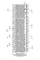
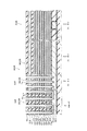
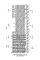
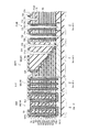
図1は、第1の実施形態に係る不揮発性半導体記憶装置の構成を例示する模式的断面図である。
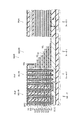
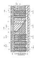
図2は、第1の実施形態に係る不揮発性半導体記憶装置の構成を例示する模式的斜視図である。
なお、図2においては、図を見易くするために、導電部分のみを示し、絶縁部分は図示を省略している。
図3は、第1の実施形態に係る不揮発性半導体記憶装置の一部の構成を例示する模式的断面図である。
(First embodiment)
FIG. 1 is a schematic cross-sectional view illustrating the configuration of the nonvolatile semiconductor memory device according to the first embodiment.
FIG. 2 is a schematic perspective view illustrating the configuration of the nonvolatile semiconductor memory device according to the first embodiment.
In FIG. 2, only the conductive portion is shown and the insulating portion is not shown for easy understanding of the drawing.
FIG. 3 is a schematic cross-sectional view illustrating the configuration of a part of the nonvolatile semiconductor memory device according to the first embodiment.
図1に表したように、本実施形態に係る不揮発性半導体記憶装置110は、情報を格納するメモリ部MUと、情報を格納しない非メモリ部PUと、を備える。
As shown in FIG. 1, the nonvolatile
メモリ部MUは、第1方向に交互に積層された複数の電極膜61と複数の電極間絶縁膜62と、を含む積層構造体MLを含む。
The memory unit MU includes a stacked structure ML including a plurality of
なお、本願明細書において、「積層」とは、複数の層が直接重ねられる場合の他、複数の層の間に他の要素が挿入されて重ねられる場合も含む。
積層構造体MLにおける電極膜61及び電極間絶縁膜62の積層方向をZ軸方向(第1方向)とする。Z軸方向に対して垂直な1つの方向をY軸方向(第2方向)とする。そして、Z軸方向とY軸方向とに対して垂直な方向をX軸方向(第3方向)とする。
In the present specification, “stacking” includes not only the case where a plurality of layers are directly stacked, but also the case where other elements are inserted between the layers and stacked.
The stacking direction of the
不揮発性半導体記憶装置110は、メモリ部MUと非メモリ部PUとが設けられる基板11をさらに備えることができる。基板11には、例えばシリコン基板などが用いられる。
The nonvolatile
Z軸方向は、基板11の主面11aに対して垂直な方向である。基板11の主面11aの上に、メモリ部MU及び非メモリ部PUが設けられる。
The Z-axis direction is a direction perpendicular to the
すなわち、非メモリ部PUは、Z軸方向に直交する方向において、メモリ部MUに併設される。非メモリ部PUは、例えば、X−Y平面内において、メモリ部MUに併設される。非メモリ部PUは、例えば、メモリ部MUに対してX軸方向において併設される。非メモリ部PUは、例えば、メモリ部MUに対してY軸方向において併設される。1つのメモリ部MUに対して複数の非メモリ部PUが設けられても良い。 That is, the non-memory unit PU is attached to the memory unit MU in a direction orthogonal to the Z-axis direction. For example, the non-memory unit PU is provided in the memory unit MU in the XY plane. For example, the non-memory unit PU is provided in the X-axis direction with respect to the memory unit MU. For example, the non-memory unit PU is provided in the Y-axis direction with respect to the memory unit MU. A plurality of non-memory units PU may be provided for one memory unit MU.
メモリ部MUにおいては、不揮発性半導体記憶装置110のメモリセルMCが設けられる。非メモリ部PUは、メモリ部MUの例えば周辺に設けられ、不揮発性半導体記憶装置110の周辺回路を含むことができる。
In memory unit MU, memory cell MC of nonvolatile
基板11において、メモリ部MUが設けられる領域をメモリ領域MURとし、非メモリ領域PURが設けられる領域を非メモリ領域PURとする。
In the
メモリ部MUは、例えば、3次元マトリクス状に配列したメモリセルトランジスタを有するマトリクスメモリセル部MU1と、マトリクスメモリセル部MU1の配線を接続する配線接続部MU2と、を有する。基板11において、マトリクスメモリセル部MU1が設けられる領域をマトリクスメモリセル領域MU1Rとし、配線接続部MU2が設けられる領域を配線接続領域MU2Rとする。
The memory unit MU includes, for example, a matrix memory cell unit MU1 having memory cell transistors arranged in a three-dimensional matrix, and a wiring connection unit MU2 that connects wirings of the matrix memory cell unit MU1. In the
図2は、マトリクスメモリセル部MU1の構成を例示している。
図1においては、マトリクスメモリセル部MU1として、図2のA−A’線断面の一部と、図2のB−B’線断面の一部が例示されている。
FIG. 2 illustrates the configuration of the matrix memory cell unit MU1.
In FIG. 1, as the matrix memory cell unit MU1, a part of the cross section along the line AA ′ in FIG. 2 and a part of the cross section along the line BB ′ in FIG. 2 are illustrated.
図1及び図2に表したように、マトリクスメモリセル部MU1においては、基板11の主面11a上に、積層構造体MLが設けられる。
As illustrated in FIGS. 1 and 2, in the matrix memory cell unit MU <b> 1, the stacked structure body ML is provided on the
不揮発性半導体記憶装置110は、選択ゲート電極SGをさらに備える。選択ゲート電極SGは、積層構造体MLとZ軸方向に沿って積層される。
The nonvolatile
本具体例においては、電極膜61は、X軸方向に沿って延在する帯状の部分を有している。また、選択ゲート電極SGも、X軸方向に沿って延在する帯状の部分を有している。
In this specific example, the
そして、積層構造体ML及び選択ゲート電極SGをZ軸方向に沿って貫通する半導体ピラーSPが設けられる。この半導体ピラーSPは、例えば、積層構造体ML及び選択ゲート電極をZ軸方向に沿って貫通する貫通ホールTHの中に半導体を埋め込むことによって形成される。半導体ピラーSPは、Z軸方向に延在する筒状(例えば円筒状)または、柱状(例えば円柱状)である。すなわち、半導体ピラーSPの内部が中空でも良く、半導体ピラーSPの内側に例えば絶縁層などが設けられても良い。 A semiconductor pillar SP that penetrates the stacked structure ML and the select gate electrode SG along the Z-axis direction is provided. The semiconductor pillar SP is formed, for example, by embedding a semiconductor in a through hole TH that penetrates the stacked structure ML and the select gate electrode along the Z-axis direction. The semiconductor pillar SP has a cylindrical shape (for example, a cylindrical shape) or a column shape (for example, a cylindrical shape) extending in the Z-axis direction. That is, the inside of the semiconductor pillar SP may be hollow, and an insulating layer or the like may be provided inside the semiconductor pillar SP.
後述するように、不揮発性半導体記憶装置110のメモリ部MUにおいては、電極膜61と半導体ピラーSPとが交差する部分において、記憶層を有するメモリセルトランジスタが形成される。メモリセルトランジスタは3次元マトリクス状に配列され、この記憶層に電荷を蓄積させることにより、各メモリセルトランジスタが情報(データ)を記憶するメモリセルMCとして機能する。
As will be described later, in the memory unit MU of the nonvolatile
すなわち、メモリ部MUは、複数の電極膜61と半導体ピラーSPとの間に設けられピラー部記憶層48pをさらに含む。
That is, the memory unit MU further includes a pillar
一方、非メモリ部PUは、ダミー導電膜65と、ダミー選択ゲート電極SGdと、第1非メモリ部コンタクト電極71pと、第2非メモリ部コンタクト電極72pと、を含む。
On the other hand, the non-memory portion PU includes a dummy
ダミー導電膜65は、複数の電極膜61(第1電極膜61a)の少なくとも1つと同層の部分65pを含む。すなわち、ダミー導電膜65の上記の部分65pは、複数の電極膜61の少なくとも1つのZ軸方向に対して垂直な面に沿って配置される。例えば、ダミー導電膜65の上記の部分65pと、基板11と、のZ軸方向に沿った距離は、複数の電極膜61のその少なくとも1つと、基板11と、のZ軸方向に沿った距離と等しい。
The dummy
ダミー選択ゲート電極SGdは、選択ゲート電極SG(第1選択ゲート電極SG1)と同層である。すなわち、ダミー選択ゲート電極SGdのZ軸方向に対して垂直な面は、選択ゲート電極SGのZ軸方向に対して垂直な面が含まれる面内に配置される。例えば、ダミー選択ゲート電極SGdと基板11とのZ軸方向に沿った距離は、選択ゲート電極SGと基板11とのZ軸方向に沿った距離と等しい。
The dummy selection gate electrode SGd is in the same layer as the selection gate electrode SG (first selection gate electrode SG1). That is, the plane perpendicular to the Z-axis direction of the dummy selection gate electrode SGd is disposed in a plane including the plane perpendicular to the Z-axis direction of the selection gate electrode SG. For example, the distance along the Z-axis direction between the dummy selection gate electrode SGd and the
第1非メモリ部コンタクト電極71pは、ダミー導電膜65に電気的に接続され、Z軸方向に沿って延在する。第2非メモリ部コンタクト電極72pは、ダミー選択ゲート電極SGdに電気的に接続されZ軸方向に沿って延在する。
The first non-memory
例えば、ダミー導電膜65は、複数の電極膜61のそれぞれと同層の複数の第1ダミー膜61dと、複数の電極間絶縁膜62と同層の複数の第2ダミー膜62dと、含むことができる。
For example, the dummy
第1ダミー膜61dは、基板11からみて、電極膜61と同じ高さに配置される。第1ダミー膜61dには、例えば、電極膜61に用いられる材料と同じ材料を用いることができる。
The
第2ダミー膜62dは、基板11からみて、電極間絶縁膜62と同じ高さに配置される。第2ダミー膜62dには、例えば、電極間絶縁膜62に用いられる材料と同じ材料を用いることができる。または、第2ダミー膜62dには、電極間絶縁膜62に用いられる材料とは異なる材料が用いられる。
The
本具体例では、第2ダミー膜62dには導電膜が用いられており、第2ダミー膜62dに、電極間絶縁膜62に用いられる材料とは異なる材料が用いられる例である。
In this specific example, a conductive film is used for the
第1ダミー膜61dが導電膜であり、第2ダミー膜62dが絶縁膜である場合は、第1ダミー膜61dと第2ダミー膜62dとの境界は比較的明確である。一方、第1ダミー膜61d及び第2ダミー膜62dが共に導電膜である場合は、第1ダミー膜61dと第2ダミー膜62dとの境界は不明確である場合がある。このように、第1ダミー膜61dと第2ダミー膜62dとが、比較的明確に区別できる場合と、明確に区別できない場合とがある。
When the
例えば、第1ダミー膜61dが、ダミー導電膜65のうちの、上記の、複数の電極膜61の少なくとも1つと同層の部分65pとなる。
For example, the
また、ダミー導電膜65のZ軸方向に沿った幅は、積層構造体ML(例えば第1積層構造体ML1)のZ軸方向に沿った幅と実質的に同じとすることができる。
Moreover, the width along the Z-axis direction of the dummy
後述するように、非メモリ部PUのダミー導電膜65は、例えば、メモリ部MUの電極膜61を形成する際に電極膜61と一緒に形成される。そして、非メモリ部PUのダミー選択ゲート電極SGdは、例えば、メモリ部MUの選択ゲート電極SGを形成する際に選択ゲート電極SGと一緒に形成される。
As will be described later, for example, the dummy
第1非メモリ部コンタクト電極71pは、配線71に接続される。第2非メモリ部コンタクト電極72pは、配線72に接続される。これにより、ダミー導電膜65は、第1非メモリ部コンタクト電極71p及び配線71を介して、所定の電位に設定される。そして、ダミー選択ゲート電極SGdは、第2非メモリ部コンタクト電極72p及び配線72を介して、所定の電位に設定される。
The first non-memory
これにより、不揮発性半導体記憶装置110内の導電層どうしの電気的な干渉が抑制され、より安定した動作が実現できる。
Thereby, electrical interference between the conductive layers in the nonvolatile
以下では、メモリ部MUの構成の例について詳しく説明する。
図1に例示したように、不揮発性半導体記憶装置110においては、基板11の主面11aの上に層間絶縁膜13が設けられ、層間絶縁膜13の上に絶縁膜13gが設けられる。なお、絶縁膜13gは、後述する周辺回路トランジスタ51のゲート絶縁膜として機能する絶縁膜である。さらに、絶縁膜13gの上に、後述の接続部導電層SCCが設けられ、接続部導電層SCCの上に積層構造体MLが設けられる。
Hereinafter, an example of the configuration of the memory unit MU will be described in detail.
As illustrated in FIG. 1, in the nonvolatile
なお、図1においては電極膜61が8枚描かれているが、積層構造体MLにおいて、設けられる電極膜61の数は任意である。なお、図2においては、図を見やすくするために、電極膜61の一部は省略されている。
In FIG. 1, eight
なお、半導体ピラーSPのうち、積層構造体MLを貫通する部分と、選択ゲート電極SGを貫通する部分と、は、連続して形成された半導体層でも良く、半導体ピラーSPのうちの積層構造体MLを貫通する部分と、半導体ピラーSPのうちの選択ゲート電極SGを貫通する部分と、が、別の工程で形成され、これらの部分が電気的に接続されていても良い。 In the semiconductor pillar SP, the portion that penetrates the stacked structure ML and the portion that penetrates the selection gate electrode SG may be a semiconductor layer formed continuously, or the stacked structure of the semiconductor pillar SP. A portion that penetrates the ML and a portion that penetrates the select gate electrode SG in the semiconductor pillar SP may be formed in separate steps, and these portions may be electrically connected.
なお、図1に表したように、積層構造体MLの最下部(例えば、基板11に最も近い側)の電極膜61の下に絶縁膜15aを設けることができ、この絶縁膜15aも積層構造体MLに含まれることができる。また、積層構造体MLの最上部(例えば、基板11から最も遠い側)の電極膜61の上にさらに絶縁膜を設けることができ、この絶縁膜も積層構造体MLに含まれることができる。なお、これらの絶縁膜には、例えば酸化シリコンを用いることができる。ただし、実施形態はこれに限らず、これらの絶縁膜の材料は任意である。
As shown in FIG. 1, an insulating
積層構造体MLと選択ゲート電極SGとの間には、層間絶縁膜16が設けられている。また、電極膜61どうしをY軸方向に沿って分断する層間絶縁膜ILPが設けられている。層間絶縁膜ILPは、X軸方向に沿って延在する。本具体例では、この層間絶縁膜ILPは、さらに選択ゲート電極SGどうしをY軸方向に沿って分断する。
An interlayer insulating
そして、選択ゲート電極SG及び層間絶縁膜ILPの上に層間絶縁膜18が設けられ、その上に、ソース線SL(第2配線WR2)とコンタクト電極22とが設けられている。ソース線SLの周りには層間絶縁膜19が設けられている。本具体例では、ソース線SLは、X軸方向に沿った帯状の形状を有している。
An interlayer insulating
そして、ソース線SLの上に層間絶縁膜23が設けられ、その上にビット線BL(第1配線WR1)が設けられている。ビット線BLは、例えば、Y軸方向に沿った帯状の形状を有している。
An interlayer insulating
その上にビット線BLの上に、層間絶縁膜25、層間絶縁膜27及びパッシベーション膜29が設けられる。
On the bit line BL, an
なお、層間絶縁膜13、16、17、18、19、23、25及び27、例えば酸化シリコンを用いることができる。また、絶縁膜13gにも酸化シリコンが用いられる。パッシベーション膜29には、例えば窒化シリコンが用いられる。
Note that
そして、本具体例においては、2本ずつの半導体ピラーSPは、基板11の側で接続されている。
すなわち、不揮発性半導体記憶装置110は、第1半導体ピラーSP1と第2半導体ピラーSP2とを基板11の側で電気的に接続する半導体接続部SCをさらに備える。半導体接続部SCには、半導体ピラーSPとなる材料を用いることができる。
In this specific example, two semiconductor pillars SP are connected on the
That is, the nonvolatile
ただし、後述するように、半導体ピラーSPのそれぞれが独立し、半導体ピラーSPどうしが接続されていなくても良い。以下では、2本ずつの半導体ピラーSPが接続される場合について説明する。 However, as will be described later, each of the semiconductor pillars SP is independent, and the semiconductor pillars SP may not be connected to each other. Hereinafter, a case where two semiconductor pillars SP are connected will be described.
このように、不揮発性半導体記憶装置110において半導体ピラーは複数設けられており、半導体ピラーの全体または任意の半導体ピラーを指す場合には、「半導体ピラーSP」と言い、特定の半導体ピラーどうしの関係を説明する際などにおいて、特定の半導体ピラーを指す場合に、「第n半導体ピラーSPn」(nは1以上の任意の整数)と言うことにする。他の構成要素も同様に、例えば、半導体接続部の全体または任意の半導体接続部を指す場合には、「半導体接続部SC」と言い、特定の半導体接続部を指す場合に「第n半導体接続部SCn」(nは1以上の任意の整数)と言う。
As described above, in the nonvolatile
図2に表したように、第1半導体接続部SC1によって接続された第1半導体ピラーSP1及び第2半導体ピラーSP2がペアとなって1つのU字形状のNANDストリングとなり、第2半導体接続部SC2によって接続された第3半導体ピラーSP3及び第4半導体ピラーSP4がペアとなって別のU字形状のNANDストリングとなる。 As shown in FIG. 2, the first semiconductor pillar SP1 and the second semiconductor pillar SP2 connected by the first semiconductor connection part SC1 are paired to form one U-shaped NAND string, and the second semiconductor connection part SC2 The third semiconductor pillar SP3 and the fourth semiconductor pillar SP4 connected together by the pair form another U-shaped NAND string.
図1に例示したように、配線接続部MU2においては、X軸方向における一方の端において、電極膜61は、メモリ部コンタクト電極31によってワード配線32に接続され、例えば基板11に設けられる駆動回路と電気的に接続される。Z軸方向に積層された各電極膜61のX軸方向における長さが階段状に変化させられ、X軸方向の一方の端で電極膜61が駆動回路と電気的に接続される。これにより、基板11からの距離が同じ電極膜61において、ペアとなる第1半導体ピラーSP1及び第2半導体ピラーSP2とで異なる電位が設定できる。これにより、第1半導体ピラーSP1と第2半導体ピラーSP2とに対応する同層のメモリセルMCは互いに独立して動作できる。第3半導体ピラーSP3及び第4半導体ピラーSP4に関しても同様である。
As illustrated in FIG. 1, in the wiring connection unit MU <b> 2, the
また、接続部導電層SCCは、例えば、メモリ部コンタクト電極33によって接続部導電層のための配線に接続される。
選択ゲート電極SGは、例えば、メモリ部コンタクト配線34によって、選択ゲート電極のための配線35に接続される。配線35の上には、層間絶縁膜25が設けられ、層間絶縁膜25の上には、配線35に接続されるメタル配線28aが設けられている。
なお、メモリ部コンタクト電極31及びメモリ部コンタクト配線34の側面は層間絶縁膜18cで覆われている。
Further, the connection portion conductive layer SCC is connected to the wiring for the connection portion conductive layer by, for example, the memory
For example, the selection gate electrode SG is connected to the
The side surfaces of the memory
図1及び図2に表したように、半導体ピラーSPの半導体接続部SCとは反対の端のそれぞれが、ビット線BLまたはソース線SLに接続され、半導体ピラーSPのそれぞれに、選択ゲート電極SG(第1〜第4選択ゲート電極SG1〜SG4)が設けられることにより、任意の半導体ピラーSPの任意のメモリセルMCに所望のデータを書き込み、また読み出すことができる。 As shown in FIGS. 1 and 2, each end of the semiconductor pillar SP opposite to the semiconductor connection portion SC is connected to the bit line BL or the source line SL, and the select gate electrode SG is connected to each semiconductor pillar SP. By providing (first to fourth select gate electrodes SG1 to SG4), desired data can be written to and read from any memory cell MC of any semiconductor pillar SP.
なお、各電極膜61に設けられる半導体ピラーSPの数は任意である。
The number of semiconductor pillars SP provided on each
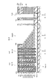
図3は、マトリクスメモリセル部MU1の構成を例示しており、例えば図1のB1−B2線断面の一部に相当する断面図である。
図3に表したように、不揮発性半導体記憶装置110において、メモリ部MUは、第1積層構造体ML1と、第1選択ゲート電極SG1と、第1半導体ピラーSP1と、第1ピラー部記憶層48p1と、を含む。
FIG. 3 exemplifies the configuration of the matrix memory cell unit MU1, and is a cross-sectional view corresponding to, for example, part of the cross section along line B1-B2 of FIG.
As illustrated in FIG. 3, in the nonvolatile
第1積層構造体ML1は、Z軸方向に積層された複数の第1電極膜61aと、複数の第1電極膜61aどうしの間に設けられた第1電極間絶縁膜62aと、を含む。第1選択ゲート電極SG1は、第1積層構造体ML1とZ軸方向に沿って積層される。第1半導体ピラーSP1は、第1積層構造体ML1及び第1選択ゲート電極SG1をZ軸方向に沿って貫通する。第1ピラー部記憶層48p1は、複数の第1電極膜61aと第1半導体ピラーSP1との間に設けられる。
The first stacked structure ML1 includes a plurality of
さらに、メモリ部MUは、第1ピラー部外側絶縁膜43p1と、第1ピラー部内側絶縁膜42p1と、を含む。第1ピラー部外側絶縁膜43p1は、第1ピラー部記憶層48p1と複数の第1電極膜61aとの間に設けられる。第1ピラー部内側絶縁膜42p1は、第1ピラー部記憶層48p1と第1半導体ピラーSP1との間に設けられる。
Further, the memory unit MU includes a first pillar unit outer insulating film 43p1 and a first pillar unit inner insulating film 42p1. The first pillar portion outer insulating film 43p1 is provided between the first pillar portion storage layer 48p1 and the plurality of
さらに、メモリ部MUは、第2積層構造体ML2と、第2選択ゲート電極SG2と、第2半導体ピラーSP2と、第2ピラー部記憶層48p2と、半導体接続部SC(第1半導体接続部SC1)と、を含む。 Further, the memory unit MU includes a second stacked structure ML2, a second select gate electrode SG2, a second semiconductor pillar SP2, a second pillar unit storage layer 48p2, and a semiconductor connection unit SC (first semiconductor connection unit SC1). ) And.
第2積層構造体ML2は、Z軸方向に対して垂直なY軸方向において第1積層構造体MLと隣接する。第2積層構造体ML2は、Z軸方向に積層された複数の第2電極膜61bと、複数の第2電極膜61bどうしの間に設けられた第2電極間絶縁膜62bと、を含む。第2選択ゲート電極SG2は、第2積層構造体ML2とZ軸方向に沿って積層される。第2半導体ピラーSP2は、第2積層構造体ML2及び第2選択ゲート電極SG2をZ軸方向に沿って貫通する。第2ピラー部記憶層48p2は、複数の第2電極膜61bと第2半導体ピラーSP2との間に設けられる。
半導体接続部SCは、第1半導体ピラーSP1の一端と、第2半導体ピラーSP2の一端と、を接続する。
The second stacked structure body ML2 is adjacent to the first stacked structure body ML in the Y-axis direction perpendicular to the Z-axis direction. The second stacked structure ML2 includes a plurality of
The semiconductor connection part SC connects one end of the first semiconductor pillar SP1 and one end of the second semiconductor pillar SP2.
さらに、メモリ部MUは、第2ピラー部外側絶縁膜43p2と、第2ピラー部内側絶縁膜42p2と、を含む。第2ピラー部外側絶縁膜43p2は、第2ピラー部記憶層48p2と複数の第2電極膜61bとの間に設けられる。第2ピラー部内側絶縁膜42p2は、第2ピラー部記憶層48p2と第2半導体ピラーSP2との間に設けられる。
Further, the memory unit MU includes a second pillar unit outer insulating film 43p2 and a second pillar unit inner insulating film 42p2. The second pillar portion outer insulating film 43p2 is provided between the second pillar portion storage layer 48p2 and the plurality of
さらに、メモリ部MUは、半導体接続部SC(第1半導体接続部SC1)に対向する接続部導電層SCCを含む。 Furthermore, the memory unit MU includes a connection part conductive layer SCC facing the semiconductor connection part SC (first semiconductor connection part SC1).
さらに、メモリ部MUは、第1接続部記憶層48c1と、第1接続部外側絶縁膜43c1と、第1接続部内側絶縁膜42c1と、を含むことができる。第1接続部記憶層48c1は、接続部導電層SCCと半導体接続部SC(第1半導体接続部SC1)との間に設けられる。第1接続部外側絶縁膜43c1は、第1接続部記憶層48c1と接続部導電層SCCとの間に設けられる。第1接続部内側絶縁膜42c1は、第1接続部記憶層48c1と第1半導体接続部SC1との間に設けられる。 Further, the memory unit MU may include a first connection unit storage layer 48c1, a first connection unit outer insulating film 43c1, and a first connection unit inner insulating film 42c1. The first connection part storage layer 48c1 is provided between the connection part conductive layer SCC and the semiconductor connection part SC (first semiconductor connection part SC1). The first connection portion outer insulating film 43c1 is provided between the first connection portion storage layer 48c1 and the connection portion conductive layer SCC. The first connection portion inner insulating film 42c1 is provided between the first connection portion storage layer 48c1 and the first semiconductor connection portion SC1.
ここで、第1ピラー部外側絶縁膜43p1、第1ピラー部記憶層48p1及び第1ピラー部内側絶縁膜42p1の積層膜を、積層絶縁膜47とする。積層絶縁膜47は、第2ピラー部外側絶縁膜43p2、第2ピラー部記憶層48p2及び第2ピラー部内側絶縁膜42p2の積層膜ともなる。また、積層絶縁膜47は、第1接続部外側絶縁膜43c1、第1接続部記憶層48c1及び第1接続部内側絶縁膜42c1の積層膜ともなる。
Here, a laminated film of the first pillar portion outer insulating film 43p1, the first pillar portion memory layer 48p1, and the first pillar portion inner insulating film 42p1 is referred to as a laminated insulating
なお、複数の第1電極膜61aのそれぞれと、複数の第2電極膜61bのそれぞれと、は、同層である。すなわち、基板11と、複数の第1電極膜61aのそれぞれと、の距離は、基板11と、複数の第2電極膜61bのそれぞれと、の距離と、同じである。なお、基板11と、複数の第1電極間絶縁膜62aのそれぞれと、の距離は、基板11と、複数の第2電極間絶縁膜62bのそれぞれと、の距離と、同じである。
Each of the plurality of
電極膜61(第1電極膜61a及び第2電極膜61b)と、半導体ピラーSP(第1半導体ピラーSP1及び第2半導体ピラーSP2)と、が交差する部分に、メモリセルトランジスタが形成され、このメモリセルトランジスタのそれぞれがメモリセルMCとなる。
A memory cell transistor is formed at a portion where the electrode film 61 (
電極膜61には所定の電気信号が印加され、電極膜61は、不揮発性半導体記憶装置110のワード電極として機能する。
A predetermined electrical signal is applied to the
メモリセルMCのそれぞれにおいて、記憶層48(第1ピラー部記憶層48p1及び第2ピラー部記憶層48p1)は、半導体ピラーSPと電極膜61との間に印加される電界によって電荷を蓄積または放出し、情報を記憶する部分として機能する。すなわち、記憶層48(第1ピラー部記憶層48p1及び第2ピラー部記憶層48p2)は、電荷蓄積層として機能する。
In each of the memory cells MC, the storage layer 48 (the first pillar portion storage layer 48p1 and the second pillar portion storage layer 48p1) accumulates or emits charges by an electric field applied between the semiconductor pillar SP and the
内側絶縁膜42(第1ピラー部内側絶縁膜42p1及び第2ピラー部内側絶縁膜42p2)は、メモリセルMCのそれぞれにおいてトンネル絶縁膜として機能する。 The inner insulating film 42 (the first pillar inner insulating film 42p1 and the second pillar inner insulating film 42p2) functions as a tunnel insulating film in each of the memory cells MC.
外側絶縁膜43(第1ピラー部外側絶縁膜43p1及び第2ピラー部外側絶縁膜43p2)は、メモリセルMCのそれぞれにおいてブロック絶縁膜として機能する。 The outer insulating film 43 (the first pillar portion outer insulating film 43p1 and the second pillar portion outer insulating film 43p2) functions as a block insulating film in each of the memory cells MC.
接続部記憶層48c(第1接続部記憶層48c1)には、第1ピラー部記憶層48p1及び第2ピラー部記憶層48p2に用いられる材料と同じ材料を用いることができる。接続部記憶層48c(第1接続部記憶層48c1)は、第1ピラー部記憶層48p1及び第2ピラー部記憶層48p2と同時に形成されることができる。 For the connection part memory layer 48c (first connection part memory layer 48c1), the same material as that used for the first pillar part memory layer 48p1 and the second pillar part memory layer 48p2 can be used. The connection portion storage layer 48c (first connection portion storage layer 48c1) can be formed simultaneously with the first pillar portion storage layer 48p1 and the second pillar portion storage layer 48p2.
第1接続部内側絶縁膜42c1には、第1ピラー部内側絶縁膜42p1及び第2ピラー部内側絶縁膜42p2に用いられる材料と同じ材料を用いることができる。第1接続部内側絶縁膜42c1は、第1ピラー部内側絶縁膜42p1及び第2ピラー部内側絶縁膜42p2と同時に形成されることができる。 The same material as that used for the first pillar inner insulating film 42p1 and the second pillar inner insulating film 42p2 can be used for the first connection inner insulating film 42c1. The first connecting portion inner insulating film 42c1 may be formed simultaneously with the first pillar inner insulating film 42p1 and the second pillar inner insulating film 42p2.
第1接続部外側絶縁膜43c1には、第1ピラー部外側絶縁膜43p1及び第2ピラー部外側絶縁膜43p2に用いられる材料と同じ材料を用いることができる。第1接続部外側絶縁膜43c1は、第1ピラー部外側絶縁膜43p1及び第2ピラー部外側絶縁膜43p2と同時に形成されることができる。 For the first connection portion outer insulating film 43c1, the same material as that used for the first pillar portion outer insulating film 43p1 and the second pillar portion outer insulating film 43p2 can be used. The first connection portion outer insulating film 43c1 may be formed simultaneously with the first pillar portion outer insulating film 43p1 and the second pillar portion outer insulating film 43p2.
接続部導電層SCCに与えられる電圧によって、半導体接続部SC(第1半導体接続部SC1)により、第1半導体ピラーSP1と第2半導体ピラーSP2とが電気的に接続される。 The first semiconductor pillar SP1 and the second semiconductor pillar SP2 are electrically connected by the semiconductor connection portion SC (first semiconductor connection portion SC1) by the voltage applied to the connection portion conductive layer SCC.
接続部導電層SCCと第1半導体接続部SC1とが対向する部分を、第1接続部記憶層48c1を電荷蓄積層として含むメモリセルMCとして利用しても良い。すなわち、接続部記憶層48c(第1接続部記憶層48c1)は、半導体接続部SCと接続部導電層SCCとの間に印加される電界よって電荷を蓄積または放出し、情報を記憶する部分として機能することができる。 A portion where the connection portion conductive layer SCC and the first semiconductor connection portion SC1 face each other may be used as a memory cell MC including the first connection portion storage layer 48c1 as a charge storage layer. In other words, the connection portion storage layer 48c (first connection portion storage layer 48c1) stores or stores information by accumulating or discharging charges by an electric field applied between the semiconductor connection portion SC and the connection portion conductive layer SCC. Can function.
電極膜61(第1電極膜61a及び第2電極膜61b)及び接続部導電層SCCには、任意の導電材料を用いることができ、例えば、不純物が導入されて導電性が付与されたアモルファスシリコン(非晶質シリコン)、または、不純物が導入されて導電性が付与されたポリシリコン(多結晶シリコン)などを用いることができ、また、金属及び合金なども用いることができる。
For the electrode film 61 (the
電極間絶縁膜62(第1電極間絶縁膜62a及び第2電極間絶縁膜62b)、内側絶縁膜42(第1ピラー部内側絶縁膜42p1、第2ピラー部内側絶縁膜42p2及び第1接続部内側絶縁膜42c1)、及び、外側絶縁膜43(第1ピラー部外側絶縁膜43p1、第2ピラー部外側絶縁膜43p2及び第1接続部外側絶縁膜43c1)には、例えば酸化シリコンを用いることができる。これらの膜は、単層膜でも良く、また積層膜でも良い。
Interelectrode insulating film 62 (first interelectrode
記憶層48(第1ピラー部記憶層48p1、第2ピラー部記憶層48p2及び第1接続部記憶層48c1)には、例えば窒化シリコンを用いることができる。記憶層48は単層膜でも良く、また積層膜でも良い。
For example, silicon nitride can be used for the memory layer 48 (the first pillar memory layer 48p1, the second pillar memory layer 48p2, and the first connection memory layer 48c1). The
なお、電極間絶縁膜62、内側絶縁膜42、外側絶縁膜43及び記憶層48には、上記に例示した材料に限らず、任意の材料を用いることができる。
The interelectrode
選択ゲート電極SG(第1選択ゲート電極SG1及び第2選択ゲート電極SG2)には、任意の導電材料を用いることができ、例えば、不純物が導入されて導電性が付与されたアモルファスシリコン(非晶質シリコン)、または、不純物が導入されて導電性が付与されたポリシリコン(多結晶シリコン)などを用いることができ、また、金属及び合金なども用いることができる。 For the selection gate electrode SG (the first selection gate electrode SG1 and the second selection gate electrode SG2), any conductive material can be used. For example, amorphous silicon (amorphous silicon to which conductivity is imparted by introducing impurities) High-quality silicon) or polysilicon doped with conductivity by introducing impurities (polycrystalline silicon), or a metal, an alloy, or the like can also be used.
選択ゲート電極SGと半導体ピラーSPとの間に選択ゲート絶縁膜SGIが設けられる。 A selection gate insulating film SGI is provided between the selection gate electrode SG and the semiconductor pillar SP.
選択ゲート絶縁膜SGI(第1選択ゲート絶縁膜SGI1及び第2選択ゲート絶縁膜SGI2)には、内側絶縁膜42、記憶層48及び外側絶縁膜43の積層膜を用いても良く、また、内側絶縁膜42、記憶層48及び外側絶縁膜43の積層膜とは異なる絶縁膜を用いても良い。選択ゲート絶縁膜SGIは、単層膜でも良く、積層膜でも良い。
As the selection gate insulating film SGI (the first selection gate insulating film SGI1 and the second selection gate insulating film SGI2), a laminated film of the inner insulating
不揮発性半導体記憶装置110は、第1配線WR1(ビット線BL)と、第2配線WR2(ソース線SL)と、をさらに備えることができる。
The nonvolatile
ビット線BLは、第1半導体ピラーSP1の他端(半導体接続部SCすなわち第1半導体接続部SC1とは反対の側の端)に電気的に接続される。
本具体例では、ビット線BLは、第1選択ゲート電極SG1の側のコンタクト電極22aと、ビット線BLの側のコンタクト電極24aと、を介して、第1半導体ピラーSP1の他端と電気的に接続される。コンタクト電極22a及びコンタクト電極24aが、図2に例示したコンタクト電極22(図1に例示したコンタクト電極VA1)に相当する。
The bit line BL is electrically connected to the other end of the first semiconductor pillar SP1 (the end on the side opposite to the semiconductor connection portion SC, that is, the first semiconductor connection portion SC1).
In this specific example, the bit line BL is electrically connected to the other end of the first semiconductor pillar SP1 via the contact electrode 22a on the first select gate electrode SG1 side and the contact electrode 24a on the bit line BL side. Connected to. The contact electrode 22a and the contact electrode 24a correspond to the
ソース線SLは、第2半導体ピラーSP2の他端(半導体接続部SCすなわち第1半導体接続部SC1とは反対の側の端)に電気的に接続される。
本具体例では、ソース線SLは、コンタクト電極22bを介して、第2半導体ピラーSP2の他端と電気的に接続される。
The source line SL is electrically connected to the other end of the second semiconductor pillar SP2 (the end on the side opposite to the semiconductor connection portion SC, that is, the first semiconductor connection portion SC1).
In this specific example, the source line SL is electrically connected to the other end of the second semiconductor pillar SP2 through the contact electrode 22b.
本具体例では、第1電極膜61a及び第2電極膜61bは、第1方向(Z軸方向)と第2方向(Y軸方向)とに対して垂直な第3方向(X軸方向)に延在する。ビット線BLは、Y軸方向に沿って延在する。一方、ソース線SLは、X軸方向に沿って延在している。
In this specific example, the
さらに、第1選択ゲート電極SG1及び第2選択ゲート電極SG2は、X軸方向に沿って延在する。すなわち、第1選択ゲート電極SG1及び第2選択ゲート電極SG2は、第1電極膜61a及び第2電極膜61bの延在方向に対して平行な方向に沿って延在する。
Further, the first selection gate electrode SG1 and the second selection gate electrode SG2 extend along the X-axis direction. That is, the first selection gate electrode SG1 and the second selection gate electrode SG2 extend along a direction parallel to the extending direction of the
第1選択ゲート電極SG1と第1半導体ピラーSP1とが交差する部分に第1選択ゲートトランジスタSGT1が形成され、第2選択ゲート電極SG2と第2半導体ピラーSP2とが交差する部分に第2選択ゲートトランジスタSGT2が形成される。選択ゲート絶縁膜SGIは、これらの選択ゲートトランジスタのゲート絶縁膜として機能する。これらの選択ゲートトランジスタは、半導体ピラーSPを選択する機能を有する。 A first selection gate transistor SGT1 is formed at a portion where the first selection gate electrode SG1 and the first semiconductor pillar SP1 intersect, and a second selection gate is formed at a portion where the second selection gate electrode SG2 and the second semiconductor pillar SP2 intersect. Transistor SGT2 is formed. The selection gate insulating film SGI functions as a gate insulating film of these selection gate transistors. These selection gate transistors have a function of selecting the semiconductor pillar SP.
図2に例示したように、不揮発性半導体記憶装置110は、第3半導体ピラーSP3と、第4半導体ピラーSP4と、第2半導体接続部SC2と、をさらに備えることができる。
As illustrated in FIG. 2, the nonvolatile
第3半導体ピラーSP3は、Y軸方向において、第2半導体ピラーSP2の第1半導体ピラーSP1とは反対の側で第2半導体ピラーSP2と隣接する。第4半導体ピラーSP4は、Y軸方向において、第3半導体ピラーSP3の第2半導体ピラーSP2とは反対の側で第3半導体ピラーSP3と隣接する。 The third semiconductor pillar SP3 is adjacent to the second semiconductor pillar SP2 on the opposite side of the second semiconductor pillar SP2 from the first semiconductor pillar SP1 in the Y-axis direction. The fourth semiconductor pillar SP4 is adjacent to the third semiconductor pillar SP3 on the opposite side of the third semiconductor pillar SP3 from the second semiconductor pillar SP2 in the Y-axis direction.
第3半導体ピラーSP3、第4半導体ピラーSP4及び第2半導体接続部SC2には、第1半導体ピラーSP1、第2半導体ピラーSP2及び第1半導体接続部SC1に関して説明した構成のそれぞれを適用できる。 Each of the configurations described with respect to the first semiconductor pillar SP1, the second semiconductor pillar SP2, and the first semiconductor connection portion SC1 can be applied to the third semiconductor pillar SP3, the fourth semiconductor pillar SP4, and the second semiconductor connection portion SC2.
すなわち、第3半導体ピラーSP3は、第3積層構造体をZ軸方向に沿って貫通する。第4半導体ピラーSP4は、第4積層構造体をZ軸方向に沿って貫通する。第2半導体接続部SC2は、第3半導体ピラーSP3の一端と、第4半導体ピラーSP4の一端とを電気的に接続する。 That is, the third semiconductor pillar SP3 penetrates the third stacked structure body along the Z-axis direction. The fourth semiconductor pillar SP4 penetrates the fourth stacked structure body along the Z-axis direction. The second semiconductor connection portion SC2 electrically connects one end of the third semiconductor pillar SP3 and one end of the fourth semiconductor pillar SP4.
第1配線(ビット線BL)は、例えば第4半導体ピラーSP4の第2半導体接続部SC2とは反対の側の他端とさらに接続される。第2配線(ソース線SL)は、第3半導体ピラーSP3の第2半導体接続部SC2とは反対の側の他端とさらに接続される。 For example, the first wiring (bit line BL) is further connected to the other end of the fourth semiconductor pillar SP4 on the side opposite to the second semiconductor connection portion SC2. The second wiring (source line SL) is further connected to the other end of the third semiconductor pillar SP3 on the side opposite to the second semiconductor connection portion SC2.
なお、図1に例示したように、第1半導体ピラーSP1は、コンタクト電極VA1によってビット線BLに接続され、第4半導体ピラーSP4は、コンタクト電極VA2によってビット線BLに接続される。 As illustrated in FIG. 1, the first semiconductor pillar SP1 is connected to the bit line BL by the contact electrode VA1, and the fourth semiconductor pillar SP4 is connected to the bit line BL by the contact electrode VA2.
以下、非メモリ部PUの例について説明する。
図1に表したように、非メモリ部PUは、すでに説明したダミー導電膜65、ダミー選択ゲート電極SGd、第1非メモリ部コンタクト電極71p及び第2非メモリ部コンタクト電極72pに加え、周辺回路部PCUをさらに含む。周辺回路部PCUは、基板11とダミー導電膜65との間に設けられた周辺回路トランジスタ51を含む。
Hereinafter, an example of the non-memory unit PU will be described.
As shown in FIG. 1, the non-memory unit PU includes peripheral circuits in addition to the dummy
すなわち、基板11(例えばシリコン基板)の主面11aの側に素子分離絶縁層(STI:Shallow Trench Isolation)として層間絶縁膜13が設けられ、層間絶縁膜13によって、基板11(シリコン基板)の主面11aの側の部分が分断される。STIによって分断された基板11の上に、絶縁膜13gが設けられ、その上に周辺回路ゲート電極52が設けられる。周辺回路ゲート電極52に対向する絶縁膜13gが、周辺回路トランジスタ51のゲート絶縁膜となり、周辺回路ゲート電極52が、周辺回路トランジスタ51のゲート電極となる。
That is, an
周辺回路ゲート電極52は、例えば、メモリ部MUの接続部導電層SCCと同層であり、周辺回路ゲート電極52には、例えば、メモリ部MUの接続部導電層SCCとなる材料と同じ材料が用いられる。
The peripheral
周辺回路ゲート電極52は、例えば、コンタクト電極73pを介して、配線73に接続される。
The peripheral
基板11(シリコン基板)のうちの、周辺回路部PCUの別の一部となる部分が、コンタクト電極74pを介して配線74に接続される。
A portion of the substrate 11 (silicon substrate) which is another part of the peripheral circuit unit PCU is connected to the
コンタクト電極73p及びコンタクト電極74pは、ダミー導電膜65及びダミー選択ゲート電極SGdをZ軸方向に沿って貫通する。
The
コンタクト電極73pとダミー導電膜65との間、及び、コンタクト電極73pとダミー選択ゲート電極SGdとの間には層間絶縁膜73Iが設けられる。コンタクト電極74pとダミー導電膜65との間、及び、コンタクト電極74pとダミー選択ゲート電極SGdとの間には層間絶縁膜74Iが設けられる。
An interlayer insulating film 73I is provided between the
このように、非メモリ部PUは、周辺回路コンタクト電極(コンタクト電極73p)と、周辺回路コンタクト層間絶縁膜(層間絶縁膜73I)と、をさらに含む。周辺回路コンタクト電極(コンタクト電極73p)は、周辺回路トランジスタ51のゲート電極(周辺回路ゲート電極52)に電気的に接続され、Z軸方向に沿って延在する。周辺回路コンタクト層間絶縁膜(層間絶縁膜73I)は、周辺回路コンタクト電極(コンタクト電極73p)と、ダミー導電膜65及びダミー選択ゲート電極SGdと、の間に設けられる。
As described above, the non-memory unit PU further includes the peripheral circuit contact electrode (
さらに、非メモリ部PUは、周辺回路基板コンタクト電極(コンタクト電極74p)と、周辺回路基板コンタクト層間絶縁膜(層間絶縁膜74I)と、をさらに含むことができおる。周辺回路基板コンタクト電極(コンタクト電極74p)は、基板11に電気的に接続され、Z軸方向に沿って延在する。周辺回路基板コンタクト層間絶縁膜(層間絶縁膜74I)は、周辺回路基板コンタクト電極(コンタクト電極74p)と、ダミー導電膜65及びダミー選択ゲート電極SGdと、の間に設けられる。
Further, the non-memory portion PU can further include a peripheral circuit board contact electrode (
なお、周辺回路部PCUには、このような構成を有する周辺回路トランジスタ51を複数設けることができる。周辺回路部PCUは、例えば、メモリ部MUに含まれる種々の導電層の電位の制御及び導電層への電流の供給などを行うことができる。
The peripheral circuit unit PCU can be provided with a plurality of
周辺回路トランジスタ51の周囲には、層間絶縁膜53が設けられる。層間絶縁膜53の上に、既に説明したダミー導電膜65、ダミー選択ゲート電極SGd、第1非メモリ部コンタクト電極71p及び第2非メモリ部コンタクト電極72pが設けられる。
An interlayer insulating
なお、ダミー選択ゲート電極SGdの上に層間絶縁膜18、層間絶縁膜19及び層間絶縁膜23が設けられ、層間絶縁膜23の上に、配線71、配線72、配線73及び配線74が設けられる。配線71、配線72、配線73及び配線74の相互の間には、層間絶縁膜24が設けられている。配線71、配線72、配線73及び配線74の上には、層間絶縁膜25が設けられる。層間絶縁膜25の上には、例えば配線71及び配線72に接続されたメタル配線28b、配線73に接続されたメタル配線28c、並びに、配線74に接続されたメタル配線28dが設けられる。メタル配線28b、メタル配線28c及びメタル配線28dの周囲に層間絶縁膜27が設けられ、層間絶縁膜27の上にパッシベーション膜29が設けられる。
The
このような構成を有する不揮発性半導体記憶装置110においては、メモリ部MUの電極膜61の形成の際に形成される非メモリ部PUのダミー導電膜65、及び、メモリ部MUの選択ゲート電極SGの形成の際に形成される非メモリ部PUのダミー選択ゲート電極SGdが、所定の電位に設定されることから、異なる電位をもつノード間の干渉が抑制される。
In the nonvolatile
例えば、もし、ダミー導電膜65及びダミー選択ゲート電極SGdが浮遊状態とされると、周辺回路トランジスタ51の動作のために所定の電位に制御されるべきコンタクト電極73p及びコンタクト電極74pが、ダミー導電膜65及びダミー選択ゲート電極SGdを介して電気的に干渉することがある。その結果、コンタクト電極73pの電位及びコンタクト電極74pの電位が不安定になることがある。このように、ダミー導電膜65及びダミー選択ゲート電極SGdが浮遊状態とされると、非メモリ部PUに含まれる種々の導電層の電位が不安定になることがある。さらに、ダミー導電膜65及びダミー選択ゲート電極SGdが浮遊状態とされると、メモリ部MUに含まれる種々の導電層の電位が不安定になることがある。
For example, if the dummy
これに対し、本実施形態においては、非メモリ部PUのダミー導電膜65及びダミー選択ゲート電極SGdが所定の電位に設定されるので、異なる電位をもつノード間の干渉が抑制され、安定した動作が実現できる。すなわち、不揮発性半導体記憶装置110によれば、より安定した動作を実現できる。
On the other hand, in the present embodiment, since the dummy
例えば、第1非メモリ部コンタクト電極71pの電位、及び、第2非メモリ部コンタクト電極72pの電位は、周辺回路トランジスタ51に与えられる印加電圧の最小値以上で、印加電圧の最大値以下とすることができる。これにより、例えば静電誘導などによって周辺回路トランジスタ51、コンタクト電極73p及びコンタクト電極74pに発生する電圧が、周辺回路トランジスタ51の印加電圧の範囲を超えないことで、周辺回路トランジスタ51の損傷や不安定な動作がより抑制できる。そして、層間絶縁膜のストレスを減らすことが可能となる。これにより、例えば信頼性が向上する。
For example, the potential of the first non-memory
第1非メモリ部コンタクト電極71pの電位、及び、第2非メモリ部コンタクト電極72pの電位は、周辺回路トランジスタ51に与えられる印加電圧の最小値よりも高く、印加電圧の最大値よりも低いことがさらに望ましい。これにより、周辺回路トランジスタ51の損傷や不安定な動作がさらに抑制できる。
The potential of the first non-memory
第1非メモリ部コンタクト電極71pの電位、及び、第2非メモリ部コンタクト電極72pの電位は、周辺回路トランジスタ51に与えられる印加電圧の最小値と、印加電圧の最大値と、の中間の電位であることがさらに望ましい。
The potential of the first non-memory
すなわち、第1非メモリ部コンタクト電極71pの電位と印加電圧の最小値との差と、第1非メモリ部コンタクト電極71pの電位と印加電圧の最大値との差と、は実質的に等しく設定することができる。例えば、第1非メモリ部コンタクト電極71pに印加する電圧は、周辺回路トランジスタ51に与えられる印加電圧の最小値と、印加電圧の最大値と、の中間の値に対して、プラスマイナス10%以内の値とされる。
また、第2非メモリ部コンタクト電極72pの電位と印加電圧の最小値との差と、第2非メモリ部コンタクト電極72pの電位と印加電圧の最大値との差と、は実質的に等しく設定することができる。例えは、第2非メモリ部コンタクト電極72pに印加する電圧は、周辺回路トランジスタ51に与えられる印加電圧の最小値と、印加電圧の最大値と、の中間の値に対して、プラスマイナス10%以内の値とされる。
これにより、周辺回路トランジスタ51の損傷や不安定な動作がさらに抑制できる。
That is, the difference between the potential of the first non-memory
Further, the difference between the potential of the second non-memory
Thereby, damage and unstable operation of the
また、第1非メモリ部コンタクト電極71p及び第2非メモリ部コンタクト電極72pは、基板11の電位よりも低い電位に設定されることができる。これにより、例えば素子分離耐圧を改善することができる。これにより、より安定した動作が実現できる。また、信頼性がより向上できる。
In addition, the first non-memory
なお、第1非メモリ部コンタクト電極71pの電位と、第2非メモリ部コンタクト電極72pの電位と、は、互いに同じでも良く、また異なっていても良い。例えば、第1非メモリ部コンタクト電極71pと第2非メモリ部コンタクト電極72pとは電気的に接続されることができる。
Note that the potential of the first non-memory
以下、不揮発性半導体記憶装置110の製造方法の例について説明する。
図4〜図25は、第1の実施形態に係る不揮発性半導体記憶装置の製造方法を例示する工程順模式的断面図である。
なお、これらの図においては、メモリ領域MUR(マトリクスメモリセル領域MU1R及び配線接続領域MU2R)と、非メモリ領域PURと、が示される。
Hereinafter, an example of a method for manufacturing the nonvolatile
4 to 25 are schematic cross-sectional views in order of the processes, illustrating the method for manufacturing the nonvolatile semiconductor memory device according to the first embodiment.
In these drawings, a memory region MUR (matrix memory cell region MU1R and wiring connection region MU2R) and a non-memory region PUR are shown.
図4に表したように、シリコン基板などの基板11の主面11aの上に、周辺回路トランジスタ51を含む周辺回路部PCUを形成する。すなわち、例えば、基板11の主面11aにSTIとなる層間絶縁膜13を形成し、これにより、基板11の主面11aの側において分断された半導体層が形成される。半導体層の表面に絶縁膜13gを形成し、その上に導電膜を形成する。この導電膜は、周辺回路ゲート電極52及び接続部導電層SCCとなる。この導電膜には、例えばポリシリコンが用いられる。
As shown in FIG. 4, the peripheral circuit unit PCU including the
非メモリ領域PURにおいて、この導電膜を所定の形状に加工し、周辺回路ゲート電極52を形成する。周辺回路ゲート電極52を介して半導体層に不純物をドープして、拡散領域を形成する。これにより、周辺回路トランジスタ51が形成される。そして、周辺回路トランジスタ51を覆うように、層間絶縁膜53を形成する。
In the non-memory region PUR, the conductive film is processed into a predetermined shape, and the peripheral
一方、マトリクスメモリセル領域MU1Rにおいては、上記の導電膜によって接続部導電層SCCが形成される。接続部導電層SCCのうち、半導体接続部SCが形成される領域に溝を形成し、この溝の中に埋め込み犠牲膜SCsfを埋め込む。埋め込み犠牲膜SCsfには、例えば窒化シリコンが用いられる。 On the other hand, in the matrix memory cell region MU1R, the connection conductive layer SCC is formed by the conductive film. In the connection portion conductive layer SCC, a trench is formed in a region where the semiconductor connection portion SC is formed, and a buried sacrificial film SCsf is buried in the trench. For example, silicon nitride is used for the buried sacrificial film SCsf.
次に、図5に表したように、接続部導電層SCC、犠牲膜SCsf、周辺回路トランジスタ51及び層間絶縁膜53の上に、絶縁膜15aを形成する。絶縁膜15aには例えば酸化シリコンが用いられる。
Next, as illustrated in FIG. 5, the insulating
さらに、層間絶縁膜53の上に、例えば、不純物が添加されたドープト・ポリシリコン膜61fと、不純物が添加されていないノンドープ・ポリシリコン膜62fと、を交互に繰り返して堆積して、積層構造体MLの母体となる積層膜を形成する。さらに、この積層膜の上に、層間絶縁膜16を形成し、その上に選択ゲート電極SGとなる選択ゲート電極膜SGfを形成し、その上に、層間絶縁膜18を形成する。選択ゲート電極膜SGfには、例えば、不純物が添加されたポリシリコンを用いることができる。
Further, on the
次に、図6に表したように、ドープト・ポリシリコン膜61f及びノンドープ・ポリシリコン膜62fを含む積層膜、層間絶縁膜16、選択ゲート電極膜SGf、及び、層間絶縁膜18に、リソグラフィ法とRIE(Reactive Ion Etching)法により、溝TR1を形成する。これにより、積層膜、層間絶縁膜16、選択ゲート電極膜SGf、及び、層間絶縁膜18はライン状に加工される。
Next, as shown in FIG. 6, the laminated film including the doped
次に、図7に表したように、溝TR1に絶縁膜TR1fを埋め込む。絶縁膜TR1fには、例えば窒化シリコンまたは酸化シリコンが用いられる。絶縁膜TR1fは、電極膜61どうしを分断する層間絶縁膜ILPとなる。
Next, as shown in FIG. 7, the insulating film TR1f is embedded in the trench TR1. For example, silicon nitride or silicon oxide is used for the insulating film TR1f. The insulating film TR1f becomes an interlayer insulating film ILP that divides the
次に、図8に表したように、ドープト・ポリシリコン膜61f及びノンドープ・ポリシリコン膜62fを含む積層膜、層間絶縁膜16、選択ゲート電極膜SGf、及び、層間絶縁膜18に、リソグラフィ法とRIE法により、貫通ホールTHを形成する。
Next, as shown in FIG. 8, the laminated film including the doped
次に、図9に表したように、例えば、熱燐酸溶液を用い、貫通ホールTHを介して、埋め込み犠牲膜SCsfを除去する。これにより、2つの貫通ホールTHの下部が連通する。 Next, as illustrated in FIG. 9, the buried sacrificial film SCsf is removed through the through hole TH using, for example, a hot phosphoric acid solution. Thereby, the lower part of two through-holes TH communicates.
次に、図10に表したように、メモリ領域MURにおけるノンドープ・ポリシリコン膜62fを除去する。これには、例えば、アルカリ系の薬液が用いることができる。なお、積層されている複数のドープト・ポリシリコン膜61fは、絶縁膜TR1f(層間絶縁膜ILP)で支持される。
Next, as shown in FIG. 10, the
一方、このとき、非メモリ領域PURにおけるノンドープ・ポリシリコン膜62fは除去せず、そのまま残す。非メモリ領域PURにおけるドープト・ポリシリコン膜61fが、ダミー導電膜65の第1ダミー膜61dになり、非メモリ領域PURにおけるノンドープ・ポリシリコン膜62fが、ダミー導電膜65の第2ダミー膜62dになる。すなわち、ダミー導電膜65が形成される。
On the other hand, at this time, the
そして、本具体例では、ドープト・ポリシリコン膜61fに含まれる不純物が、工程中の熱処理などによってノンドープ・ポリシリコン膜62fに拡散し、ドープト・ポリシリコン膜61f(第1ダミー膜61d)と、ノンドープ・ポリシリコン膜62f(第2ダミー膜62d)と、は、例えば一体化する。すなわち、本具体例では、ダミー導電膜65は、一体化した導電膜となり、第1ダミー膜61dと第2ダミー膜62dとの境界が不明確になる場合がある。
In this specific example, the impurity contained in the doped
なお、非メモリ領域PURにおける選択ゲート電極膜SGfが、ダミー選択ゲート電極SGdとなる。 Note that the selection gate electrode film SGf in the non-memory region PUR becomes the dummy selection gate electrode SGd.
次に、図11に表したように、複数のドープト・ポリシリコン膜61fどうしの間に、例えば、シリコン酸化膜を例えばCVD(Chemical Vapor Deposition)法により形成する。このシリコン酸化膜が電極間絶縁膜62になり、ドープト・ポリシリコン膜61fが電極膜61となる。これにより、積層構造体MLが形成される。
Next, as shown in FIG. 11, for example, a silicon oxide film is formed between the plurality of doped
なお、このとき、複数のドープト・ポリシリコン膜61fどうしの間隔(ノンドープ・ポリシリコン膜62fの厚さ)を、貫通ホールTHの径よりも小さく設定することで、貫通ホールTHが閉塞することなく、複数のドープト・ポリシリコン膜61fどうしの間を、シリコン酸化膜で埋めることができる。
At this time, the interval between the plurality of doped
その後、例えば、希フッ酸処理により、貫通ホールTHの内部の側面に堆積したシリコン酸化膜を除去する。 Thereafter, the silicon oxide film deposited on the side surface inside the through hole TH is removed by, for example, dilute hydrofluoric acid treatment.
次に、図12に表したように、上記の希フッ酸処理に連続して、積層絶縁膜47を形成し、さらに、積層絶縁膜47の形成に連続して、半導体ピラーSPとなる半導体ピラー膜SPfを形成する。すなわち、積層絶縁膜47として、第1ピラー部外側絶縁膜43p1、第2ピラー部外側絶縁膜43p2及び第1接続部外側絶縁膜43c1となる、例えばシリコン酸化膜を形成し、第1ピラー部記憶層48p1、第2ピラー部記憶層48p2及び第1接続部記憶層48c1となる、例えばシリコン窒化膜を形成し、さらに、第1ピラー部内側絶縁膜42p1、第2ピラー部内側絶縁膜42p2及び第1接続部内側絶縁膜42c1となる、例えばシリコン酸化膜を形成する。そして、半導体ピラー膜SPfとして、例えばポリシリコン膜を形成する。
Next, as illustrated in FIG. 12, the stacked insulating
なお、例えば、積層絶縁膜47の形成の後、積層絶縁膜47の表面に前処理等を施すことなく、半導体ピラー膜SPfが形成される。
For example, after the formation of the stacked insulating
そして、層間絶縁膜18の表面に形成された、シリコン酸化膜(電極間絶縁膜62となる膜)、積層絶縁膜47及び半導体ピラー膜SPfを、例えばRIE法により除去する。
Then, the silicon oxide film (film that becomes the interelectrode insulating film 62), the laminated insulating
次に、図13に表したように、貫通ホールTHに埋め込まれている半導体ピラー膜SPfの一部を例えばRIE法により後退させた後に、貫通ホールTHの上部の空間に、半導体ピラーコンタクト部SPCとなるポリシリコン膜(例えば不純物が添加されたポリシリコン膜)で埋め込み、平坦化する。これにより、U字形状を有するメモリストリングが形成される。 Next, as illustrated in FIG. 13, after a part of the semiconductor pillar film SPf embedded in the through hole TH is retreated by, for example, the RIE method, the semiconductor pillar contact portion SPC is formed in the space above the through hole TH. Is buried with a polysilicon film (for example, a polysilicon film to which an impurity is added) to be flattened. Thereby, a memory string having a U-shape is formed.
次に、図14に表したように、配線接続領域MU2Rにおいて、層間絶縁膜16、選択ゲート電極膜SGf及び層間絶縁膜18を、リソグラフィ法とRIE法を用いて除去し、積層構造体MLの上面を露出させる。
Next, as illustrated in FIG. 14, in the wiring connection region MU2R, the
次に、図15に表したように、層間絶縁膜18aを形成する。この層間絶縁膜18aには、例えば酸化シリコンを用いることができる。
Next, as shown in FIG. 15, an
次に、図16に表したように、配線接続領域MU2Rにおいて、レジスト膜のスリミングとRIEとを繰り返すことにより、電極膜61の端部を階段状に加工する。
Next, as shown in FIG. 16, in the wiring connection region MU <b> 2 </ b> R, the resist film slimming and RIE are repeated to process the end portion of the
次に、図17に表したように、コンタクト電極73pが形成される部分の積層膜(層間絶縁膜18a、層間絶縁膜18、ダミー選択ゲート電極SGd、層間絶縁膜16及びダミー導電膜65)に開口部73oを形成し、コンタクト電極74pが形成される部分の積層膜(層間絶縁膜18a、層間絶縁膜18、ダミー選択ゲート電極SGd、層間絶縁膜16及びダミー導電膜65)に開口部74oを形成する。
Next, as shown in FIG. 17, the stacked film (
次に、図18に表したように、開口部73o及び開口部74oの内壁面にストッパ膜18bとして、例えば窒化シリコン膜を形成する。ストッパ膜18bは、層間絶縁膜18a、及び、配線接続領域MU2Rにおいて露出している電極膜61の上にも形成される。その後、さらに、ストッパ膜18bの上に層間絶縁膜18cを形成し、平坦化する。これにより、ストッパ膜18bの上面の一部が露出する。層間絶縁膜18cには、例えば、酸化シリコンが用いられる。
Next, as illustrated in FIG. 18, for example, a silicon nitride film is formed as a
次に、図19に表したように、例えばRIE法により、表面のストッパ膜18b、及び、層間絶縁膜18cの表面部分を除去する。
Next, as shown in FIG. 19, the
次に、図20に表したように、例えばプラズマCVD法を用い層間絶縁膜19となるシリコン酸化膜を形成した後、配線接続領域MU2Rにおいては、電極膜61に接続されるメモリ部コンタクト電極31のためのコンタクトホール31o、及び、接続部導電層SCCに接続されるメモリ部コンタクト電極33のためのコンタクトホール33oを形成する。さらに、非メモリ領域PURにおいては、ダミー導電膜65に接続される第1非メモリ部コンタクト電極71pのための開口部71o、及び、ダミー選択ゲート電極SGdに接続される第2非メモリ部コンタクト電極72pのための開口部72oを形成する。
Next, as shown in FIG. 20, for example, after forming a silicon oxide film to be the interlayer insulating
次に、図21に表したように、層間絶縁膜19及び層間絶縁膜18aのうちのソース線SLとなる部分に溝SLtを形成する。そして、層間絶縁膜19及び層間絶縁膜18aのうちの選択ゲート電極SGと接続されるメモリ部コンタクト配線34となる部分に溝34tを形成する。そして、層間絶縁膜19及び層間絶縁膜18aのうちの、メモリ部コンタクト電極31、メモリ部コンタクト電極33、第1非メモリ部コンタクト電極71p、第2非メモリ部コンタクト電極72p、コンタクト電極73p、及び、コンタクト電極74pのそれぞれの接続部分となる部分に、それぞれ、溝31t、溝33t、溝71t、溝72t、溝73t、溝74tを形成する。
Next, as illustrated in FIG. 21, a trench SLt is formed in a portion of the
次に、図22に表したように、溝SLt、溝34t、溝31t、溝33t、溝71t、溝72t、溝73t、溝74t、コンタクトホール31o、コンタクトホール33o、開口部71o、開口部72o、開口部73oの残余の空間、及び、開口部74oの残余の空間に導電膜を埋め込む。この導電膜には、例えば、Ti膜−TiN膜−W膜の積層膜が用いられる。そして、導電膜の上面をCMP(Chemical Mechanical Polishing)法により除去する。このように、デュアルダマシン工程により、コンタクトプラグと配線とが同時に形成される。
Next, as shown in FIG. 22, the groove SLt, the groove 34t, the
すなわち、ソース線SL、メモリ部コンタクト配線34、メモリ部コンタクト電極31の接続部31c、メモリ部コンタクト電極33の接続部33c、第1非メモリ部コンタクト電極71pの接続部71c、第2非メモリ部コンタクト電極72pの接続部72c、コンタクト電極73pの接続部73c、コンタクト電極74pの接続部74c、メモリ部コンタクト電極31、メモリ部コンタクト電極33、第1非メモリ部コンタクト電極71p、第2非メモリ部コンタクト電極72p、コンタクト電極73p、コンタクト電極74p、が同時に形成される。
That is, the source line SL, the memory
なお、コンタクト電極73pと、ダミー導電膜65及びダミー選択電極SGdと、の間に、ストッパ膜18b及び層間絶縁膜18cが挿入されている。このストッパ膜18b及び層間絶縁膜18cが、層間絶縁膜73Iとなる。これにより、コンタクト電極73pと、ダミー導電膜65及びダミー選択ゲート電極SGdと、が電気的に遮断される。
A
また、コンタクト電極74pと、ダミー導電膜65及びダミー選択電極SGdと、の間に、ストッパ膜18b及び層間絶縁膜18cが挿入されている。このストッパ膜18b及び層間絶縁膜18cが、層間絶縁膜74Iとなる。これにより、コンタクト電極74pと、ダミー導電膜65及びダミー選択ゲート電極SGdと、が電気的に遮断される。
A
このように、周辺回路コンタクト層間絶縁膜(層間絶縁膜73I)は、シリコン窒化膜とシリコン酸化膜との積層膜を含むことができる。これにより、コンタクト電極73pと、ダミー導電膜65及びダミー選択電極SGdと、の間の高い絶縁性が実現できる。そして、周辺回路基板コンタクト層間絶縁膜(層間絶縁膜74I)は、シリコン窒化膜とシリコン酸化膜との積層膜を含むことができる。これにより、コンタクト電極74pと、ダミー導電膜65及びダミー選択電極SGdと、の間の高い絶縁性が実現できる。
Thus, the peripheral circuit contact interlayer insulating film (interlayer insulating film 73I) can include a laminated film of a silicon nitride film and a silicon oxide film. Thereby, high insulation between the
次に、図23に表したように、層間絶縁膜23を形成し、リソグラフィ法とRIE法とにより開孔を形成し、その開口の内部に導電膜を埋め込む。この導電膜には、例えば、TiN膜−TiN膜−W膜の積層膜を用いることができる。さらにその導電膜の上部をCMPにより除去する。これにより、ソース線SLのレベルの導電層への接続部が形成される。そして、それと同時に、ビット線BLに接続される半導体ピラーSP(第1半導体ピラーSP1及び第4半導体ピラーSP4など)の上部にコンタクトプラグ(コンタクト電極VA1及びVA2の一部)が形成される。
Next, as shown in FIG. 23, an
次に、図24に表したように、層間絶縁膜24を形成し、リソグラフィ法とRIE法とにより、ビット線BLに相当する分部に溝を形成した後、その溝の内部に導電膜を埋め込む。この導電膜には、例えばTa膜−TaN膜−Cu膜の積層膜が用いられる。そして、この導電膜の上部をCMPによって除去する。これにより、ビット線BL、及び、ビット線BLと同層の配線(ワード配線32、配線35、配線71、配線72、配線73及び配線74)が形成される。
Next, as shown in FIG. 24, an
次に、図25に表したように、層間絶縁膜25を形成し、層間絶縁膜25のレベルの配線へのコンタクトプラグとなる開孔部を形成し、この開口部に導電膜を埋め込む。この導電膜には、例えばTi膜−TiN膜−AlCu膜の積層膜が用いられる。そして、この積層膜を所定の形状に加工する。これにより、メタル配線28a、メタル配線28b、メタル配線28c及びメタル配線28dが形成される。また、図示しない配線層やボンディングパッドが形成される。
Next, as shown in FIG. 25, an
さらに、その上に、デバイス保護のための層間絶縁膜27(例えばシリコン酸化膜)及びパッシベーション膜29(例えばシリコン窒化膜)を形成し、さらに、これらの膜のボンディングパッドに対応する部分に開口を形成する。
以上の工程を経て、不揮発性半導体記憶装置110が製造される。
Further, an interlayer insulating film 27 (for example, a silicon oxide film) and a passivation film 29 (for example, a silicon nitride film) for device protection are formed thereon, and openings are formed in portions corresponding to the bonding pads of these films. Form.
Through the above steps, the nonvolatile
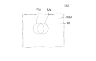
図26は、第1の実施形態に係る不揮発性半導体記憶装置の構成を例示する模式的平面図である。
すなわち、同図は、不揮発性半導体記憶装置110における、第1非メモリ部コンタクト電極71p及び第2非メモリ部コンタクト電極72pの配置を例示している。同図は、第1非メモリ部コンタクト電極71p及び第2非メモリ部コンタクト電極72pをZ軸方向に沿ってみたときの平面図である。
FIG. 26 is a schematic plan view illustrating the configuration of the nonvolatile semiconductor memory device according to the first embodiment.
That is, this figure illustrates the arrangement of the first non-memory
図26に表したように、不揮発性半導体記憶装置110においては、ダミー導電膜65に接続される第1非メモリ部コンタクト電極71pと、ダミー選択ゲート電極SGdに接続される第2非メモリ部コンタクト電極72pと、が連続しておらず、互いに独立している。すなわち、第1非メモリ部コンタクト電極71pは、Z軸方向に沿ってみたときに、第2非メモリ部コンタクト電極72pと重なる部分を有していない。
As shown in FIG. 26, in the nonvolatile
ただし、実施形態はこれに限らず、第1非メモリ部コンタクト電極71p及び第2非メモリ部コンタクト電極72pの配置は任意である。
However, the embodiment is not limited to this, and the arrangement of the first non-memory
図27は、第1の実施形態に係る別の不揮発性半導体記憶装置の構成を例示する模式的断面図である。
すなわち、同図は、本実施形態に係る別の不揮発性半導体記憶装置111における非メモリ部PUの構成を例示している。
FIG. 27 is a schematic cross-sectional view illustrating the configuration of another nonvolatile semiconductor memory device according to the first embodiment.
That is, this figure illustrates the configuration of the non-memory unit PU in another nonvolatile
図28は、第1の実施形態に係る別の不揮発性半導体記憶装置の構成を例示する模式的平面図である。
すなわち、同図は、不揮発性半導体記憶装置111における、第1非メモリ部コンタクト電極71p及び第2非メモリ部コンタクト電極72pの配置(Z軸方向に沿ってみたときの配置)を例示している。
不揮発性半導体記憶装置111におけるメモリ部MUの構成は、不揮発性半導体記憶装置110のメモリ部MUの構成と同様とすることができるので説明を省略する。
FIG. 28 is a schematic plan view illustrating the configuration of another nonvolatile semiconductor memory device according to the first embodiment.
That is, this figure illustrates the arrangement of the first non-memory
The configuration of the memory unit MU in the nonvolatile
図27及び図28に例示したように、不揮発性半導体記憶装置111においては、第1非メモリ部コンタクト電極71pのX−Y平面における位置と、第2非メモリ部コンタクト電極72pにおける位置とは実質的に同じである。すなわち、第1非メモリ部コンタクト電極71pと第2非メモリ部コンタクト電極72pとは電気的に接続される。これにより、第1非メモリ部コンタクト電極71pの電位の設定と、第2非メモリ部コンタクト電極72pの電位の設定とが、小さい面積で実施でき、有利となる。
As illustrated in FIGS. 27 and 28, in the nonvolatile
本具体例では、第2非メモリ部コンタクト電極72pのX−Y平面における外周の中に、第1非メモリ部コンタクト電極71pのX−Y平面における外周が含まれる例である。また、このような構成により、工程削減ができ、また、チップ面積の縮小が可能となる。なお、第1非メモリ部コンタクト電極71pのX−Y平面における外周の中に、第2非メモリ部コンタクト電極72pのX−Y平面における外周が含まれても良い。
In this specific example, the outer periphery in the XY plane of the first non-memory
図29は、第1の実施形態に係る別の不揮発性半導体記憶装置の構成を例示する模式的平面図である。
すなわち、同図は、本実施形態に係る別の不揮発性半導体記憶装置112における非メモリ部PUの構成を例示している。不揮発性半導体記憶装置111におけるメモリ部MUの構成は、不揮発性半導体記憶装置110のメモリ部MUの構成と同様とすることができるので説明を省略する。
FIG. 29 is a schematic plan view illustrating the configuration of another nonvolatile semiconductor memory device according to the first embodiment.
That is, this figure illustrates the configuration of the non-memory unit PU in another nonvolatile
図29に例示したように、不揮発性半導体記憶装置112においても、第1非メモリ部コンタクト電極71pと第2非メモリ部コンタクト電極72pとが連続しており、互いに電気的に接続される。
As illustrated in FIG. 29, also in the nonvolatile
本具体例では、第2非メモリ部コンタクト電極72pのX−Y平面における外周と、第1非メモリ部コンタクト電極71pのX−Y平面における外周と、が、互いに重なる。
In this specific example, the outer periphery of the second non-memory
不揮発性半導体記憶装置111及び112のように、第1非メモリ部コンタクト電極71pは、Z軸方向に沿ってみたときに、第2非メモリ部コンタクト電極72pと重なる部分を有することができる。このような構成により、チップ面積の縮小が可能となる。
Like the nonvolatile
(第2の実施の形態)
図30は、第2の実施形態に係る不揮発性半導体記憶装置の構成を例示する模式的断面図である。
図30に表したように、本実施形態に係る不揮発性半導体記憶装置120も、メモリ部MUと、非メモリ部PUと、を備える。メモリ部MUの構成は、例えば不揮発性半導体記憶装置110と同様とすることができるので説明を省略する。
(Second Embodiment)
FIG. 30 is a schematic cross-sectional view illustrating the configuration of the nonvolatile semiconductor memory device according to the second embodiment.
As shown in FIG. 30, the nonvolatile
図30に表したように、不揮発性半導体記憶装置120の非メモリ部PUにおけるダミー導電膜65の構成が不揮発性半導体記憶装置110とは異なる。
すなわち、不揮発性半導体記憶装置120においても、ダミー導電膜65は、複数の電極膜61のそれぞれと同層の複数の第1ダミー膜61dと、複数の電極間絶縁膜62と同層の複数の第2ダミー膜62dと、含む。本具体例では、第2ダミー膜62dが絶縁膜である。
As shown in FIG. 30, the configuration of the dummy
That is, also in the nonvolatile
すなわち、第2ダミー膜62dには、例えば、電極間絶縁膜62に用いられる材料と同じ材料が用いられている。また、第1ダミー膜61dには、例えば、電極膜61に用いられる材料と同じ材料が用いられている。
この場合も、ダミー導電膜65に含まれる第1ダミー膜61dが、ダミー導電膜65のうちの、複数の電極膜61の少なくとも1つと同層の部分65pとなる。
なお、この場合、図30に例示したように、第1非メモリ部コンタクト電極71pは、一番下層の第1ダミー膜61dに到達する。
That is, the same material as that used for the interelectrode insulating
Also in this case, the
In this case, as illustrated in FIG. 30, the first non-memory
このような構成を有する不揮発性半導体記憶装置120においても、非メモリ部PUのダミー導電膜65及びダミー選択ゲート電極SGdが所定の電位に設定されるので、異なる電位をもつノード間の干渉が抑制され、安定した動作が実現できる。
Even in the nonvolatile
なお、不揮発性半導体記憶装置120においても、第1非メモリ部コンタクト電極71pは、Z軸方向に沿ってみたときに、第2非メモリ部コンタクト電極72pと重なる部分を有することができ、また、有さないことができる。
Also in the nonvolatile
(第3の実施の形態)
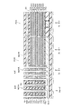
図31は、第3の実施形態に係る不揮発性半導体記憶装置の構成を例示する模式的斜視図である。
なお、図31においては、図を見易くするために、導電部分のみを示し、絶縁部分は図示を省略している。
すなわち、図31には、本実施形態に係る不揮発性半導体記憶装置130におけるマトリクスメモリセル部MU1が例示されている。
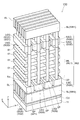
(Third embodiment)
FIG. 31 is a schematic perspective view illustrating the configuration of the nonvolatile semiconductor memory device according to the third embodiment.
In FIG. 31, only the conductive portion is shown and the insulating portion is not shown for easy understanding of the drawing.
That is, FIG. 31 illustrates the matrix memory cell unit MU1 in the nonvolatile
不揮発性半導体記憶装置130における非メモリ部PU、及び、メモリ部MUの配線接続部MU2の構成は不揮発性半導体記憶装置110、111、112及び120と同様とすることができるので説明を省略する。
Since the configurations of the non-memory unit PU and the wiring connection unit MU2 of the memory unit MU in the nonvolatile
図31に表したように、本実施形態に係る不揮発性半導体記憶装置130においては、半導体接続部SCが設けられず、半導体ピラーSPのそれぞれが独立している。すなわち、不揮発性半導体記憶装置130においては、直線状のNANDストリングが設けられる。
As shown in FIG. 31, in the nonvolatile
不揮発性半導体記憶装置130におけるメモリ部MU(マトリクスメモリセル部MU1)は、積層構造体ML(第1積層構造体ML1)と、選択ゲート電極SG(第1選択ゲート電極SG1)と、半導体ピラーSP(第1半導体ピラーSP1)と、記憶層48(第1ピラー部記憶層48p1)と、外側絶縁膜43(第1ピラー部外側絶縁膜43p1)と、内側絶縁膜42(第1ピラー部内側絶縁膜42p1)と、を含む。積層構造体MLと、半導体ピラーSP、記憶層48、外側絶縁膜43及び内側絶縁膜42の構成は第1の実施形態と同様とすることができるので説明を省略する。
The memory unit MU (matrix memory cell unit MU1) in the nonvolatile
不揮発性半導体記憶装置130のメモリ部MUにおいては、積層構造体MLの上に上部選択ゲート電極USG(第1選択ゲート電極SG1であり、例えばドレイン側選択ゲート電極SGDとなる)が設けられ、積層構造体MLの下に下部選択ゲート電極LSG(第2選択ゲート電極SG2であり、例えばソース側選択ゲート電極SGSとなる)が設けられている。
In the memory unit MU of the nonvolatile
上部選択ゲート電極USGと半導体ピラーSPとの間には上部選択ゲート絶縁膜USGI(図示しない)が設けられ、下部選択ゲート電極LSGと半導体ピラーSPとの間には、下部選択ゲート絶縁膜LSGI(図示しない)が設けられる。
選択ゲート絶縁膜SGI(図示しない)(上部選択ゲート絶縁膜USGI及び下部選択ゲート絶縁膜LSGI)には、上記の内側絶縁膜42、記憶層48及び外側絶縁膜43の積層膜を用いても良く、また、内側絶縁膜42、記憶層48及び外側絶縁膜43の積層膜とは異なる絶縁膜を用いても良い。選択ゲート絶縁膜SGIは、単層膜でも良く、積層膜でも良い。
An upper selection gate insulating film USGI (not shown) is provided between the upper selection gate electrode USG and the semiconductor pillar SP, and a lower selection gate insulating film LSGI (not shown) is provided between the lower selection gate electrode LSG and the semiconductor pillar SP. (Not shown) is provided.
As the selection gate insulating film SGI (not shown) (upper selection gate insulating film USGI and lower selection gate insulating film LSGI), a laminated film of the inner insulating
そして、下部選択ゲート電極LSGの下側に、ソース線SL(例えば第2配線WR2)が設けられている。ソース線SLの下に層間絶縁膜(図示しない)が設けられ、ソース線SLと下部選択ゲート電極LSGとの間に層間絶縁膜(図示しない)が設けられている。 A source line SL (for example, the second wiring WR2) is provided below the lower selection gate electrode LSG. An interlayer insulating film (not shown) is provided below the source line SL, and an interlayer insulating film (not shown) is provided between the source line SL and the lower select gate electrode LSG.
下部選択ゲート電極LSGの下方において半導体ピラーSPはソース線SLに接続され、上部選択ゲート電極USGの上方において半導体ピラーSPはビット線BL(例えば第1配線WR1)に接続されている。そして、上部選択ゲート電極USGと下部選択ゲート電極LSGとの間の積層構造体MLにおいて、メモリセルMCが形成される。半導体ピラーSPが、直線状の1つのメモリストリングとして機能する。 The semiconductor pillar SP is connected to the source line SL below the lower selection gate electrode LSG, and the semiconductor pillar SP is connected to the bit line BL (for example, the first wiring WR1) above the upper selection gate electrode USG. A memory cell MC is formed in the stacked structure ML between the upper selection gate electrode USG and the lower selection gate electrode LSG. The semiconductor pillar SP functions as one linear memory string.
上部選択ゲート電極USGは、層間絶縁膜(図示しない)によってY軸方向に分断されており、X軸方向に沿って延在する帯状の形状を有している。下部選択ゲート電極LSGは、層間絶縁膜(図示しない)によってY軸方向に分断されており、X軸方向に沿って延在する帯状の形状を有している。 The upper select gate electrode USG is divided in the Y-axis direction by an interlayer insulating film (not shown) and has a strip shape extending along the X-axis direction. The lower select gate electrode LSG is divided in the Y-axis direction by an interlayer insulating film (not shown) and has a strip shape extending along the X-axis direction.
一方、半導体ピラーSPの上部に接続されるビット線BL、及び、半導体ピラーSPの下部に接続されるソース線SLは、Y軸方向に延在する帯状の形状を有している。
そして、本具体例では、電極膜61は、X−Y平面に平行な板状の導電膜である。
On the other hand, the bit line BL connected to the upper part of the semiconductor pillar SP and the source line SL connected to the lower part of the semiconductor pillar SP have a strip shape extending in the Y-axis direction.
In this specific example, the
このような構成を有する不揮発性半導体記憶装置130においても、非メモリ部PUのダミー導電膜65及びダミー選択ゲート電極SGdが所定の電位に設定されるので、異なる電位をもつノード間の干渉が抑制され、安定した動作が実現できる。
Even in the nonvolatile
なお、不揮発性半導体記憶装置130においても、第1非メモリ部コンタクト電極71pは、Z軸方向に沿ってみたときに、第2非メモリ部コンタクト電極72pと重なる部分を有することができ、また、有さないことができる。
Also in the nonvolatile
以上、実施形態によれば、より安定した動作を実現する一括加工型3次元積層型の不揮発性半導体記憶装置が提供される。 As described above, according to the embodiment, a batch processing type three-dimensional stacked nonvolatile semiconductor memory device that realizes more stable operation is provided.
なお、上記においては、記憶層48として窒化シリコンを用いる場合について説明したが、実施形態はこれに限らず、記憶層48には、窒化シリコン、酸窒化シリコン、酸化アルミニウム、酸窒化アルミニウム、ハフニア、ハフニウム・アルミネート、窒化ハフニア、窒化ハフニウム・アルミネート、ハフニウム・シリケート、窒化ハフニウム・シリケート、酸化ランタン及びランタン・アルミネートよりなる群から選択されたいずれかの単層膜、または、前記群から選択された複数からなる積層膜を用いることができる。
In the above description, the case where silicon nitride is used as the
また、電極間絶縁膜62、内側絶縁膜42及び外側絶縁膜43には、酸化シリコン、窒化シリコン、酸窒化シリコン、酸化アルミニウム、酸窒化アルミニウム、ハフニア、ハフニウム・アルミネート、窒化ハフニア、窒化ハフニウム・アルミネート、ハフニウム・シリケート、窒化ハフニウム・シリケート、酸化ランタン及びランタン・アルミネートよりなる群から選択されたいずれかの単層膜、または、前記群から選択された複数からなる積層膜を用いることができる。
The inter-electrode
なお、本願明細書において、「垂直」及び「平行」は、厳密な垂直及び厳密な平行だけではなく、例えば製造工程におけるばらつきなどを含むものであり、実質的に垂直及び実質的に平行であれは良い。 In the present specification, “vertical” and “parallel” include not only strictly vertical and strictly parallel, but also include, for example, variations in the manufacturing process, and may be substantially vertical and substantially parallel. is good.
以上、具体例を参照しつつ、本発明の実施の形態について説明した。しかし、本発明は、これらの具体例に限定されるものではない。例えば、不揮発性半導体記憶装置に含まれる電極膜、電極間絶縁膜、選択ゲート電極、半導体ピラー、半導体接続部、接続部導電膜、記憶層、内側絶縁膜、外側絶縁膜、絶縁膜、導電膜、層間絶縁膜、ソース線、ビット線、配線、ダミー導電膜、ダミー電極、コンタクト電極などの各要素の具体的な構成に関しては、当業者が公知の範囲から適宜選択することにより本発明を同様に実施し、同様の効果を得ることができる限り、本発明の範囲に包含される。
また、各具体例のいずれか2つ以上の要素を技術的に可能な範囲で組み合わせたものも、本発明の要旨を包含する限り本発明の範囲に含まれる。
The embodiments of the present invention have been described above with reference to specific examples. However, the present invention is not limited to these specific examples. For example, electrode films, interelectrode insulating films, select gate electrodes, semiconductor pillars, semiconductor connection parts, connection part conductive films, storage layers, inner insulating films, outer insulating films, insulating films, conductive films included in nonvolatile semiconductor memory devices The specific structure of each element such as an interlayer insulating film, a source line, a bit line, a wiring, a dummy conductive film, a dummy electrode, and a contact electrode is similarly selected by a person skilled in the art as appropriate from a known range. As long as the same effect can be obtained, it is included in the scope of the present invention.
Moreover, what combined any two or more elements of each specific example in the technically possible range is also included in the scope of the present invention as long as the gist of the present invention is included.
その他、本発明の実施の形態として上述した不揮発性半導体記憶装置を基にして、当業者が適宜設計変更して実施し得る全ての不揮発性半導体記憶装置も、本発明の要旨を包含する限り、本発明の範囲に属する。 In addition, all nonvolatile semiconductor memory devices that can be implemented by a person skilled in the art based on the nonvolatile semiconductor memory device described above as an embodiment of the present invention as appropriate include the gist of the present invention. It belongs to the scope of the present invention.
その他、本発明の思想の範疇において、当業者であれば、各種の変更例及び修正例に想到し得るものであり、それら変更例及び修正例についても本発明の範囲に属するものと了解される。 In addition, in the category of the idea of the present invention, those skilled in the art can conceive of various changes and modifications, and it is understood that these changes and modifications also belong to the scope of the present invention. .
本発明のいくつかの実施形態を説明したが、これらの実施形態は、例として提示したものであり、発明の範囲を限定することは意図していない。これら新規な実施形態は、その他の様々な形態で実施されることが可能であり、発明の要旨を逸脱しない範囲で、種々の省略、置き換え、変更を行うことができる。これら実施形態やその変形は、発明の範囲や要旨に含まれるとともに、特許請求の範囲に記載された発明とその均等の範囲に含まれる。 Although several embodiments of the present invention have been described, these embodiments are presented by way of example and are not intended to limit the scope of the invention. These novel embodiments can be implemented in various other forms, and various omissions, replacements, and changes can be made without departing from the scope of the invention. These embodiments and modifications thereof are included in the scope and gist of the invention, and are included in the invention described in the claims and the equivalents thereof.
11…基板、 11a…主面、 13…層間絶縁膜、 13g…絶縁膜、 15a…絶縁膜、 16、18、18a、18c…層間絶縁膜、 18b…ストッパ膜、 19…層間絶縁膜、 22、22a、22b…コンタクト電極、 23、24…層間絶縁膜、 24a…コンタクト電極、 25、27…層間絶縁膜、 28a、28b、28c、28d…メタル配線、 29…パッシベーション膜、 31…メモリ部コンタクト電極、 31c…接続部、 31o…コンタクトホール、 31t…溝、 32…ワード配線、 33…メモリ部コンタクト電極、 33c…接続部、 33o…コンタクトホール、 33t…溝、 34…メモリ部コンタクト配線、 34t…溝、 35…配線、 42…内側絶縁膜、 42c…接続部内側絶縁膜、 42c1…第1接続部内側絶縁膜、 42p1、42p2…第1及び第2ピラー部内側絶縁膜、 43…外側絶縁膜、 43c…接続部外側絶縁膜、 43c1…第1接続部外側絶縁膜、 43p1、43p2…第1及び第2ピラー部外側絶縁膜、 47…積層絶縁膜、 48…記憶層、 48c…接続部記憶層、 48c1…第1接続部記憶層、 48p…ピラー部記憶層、 48p1、48p2…第1及び第2ピラー部記憶層、 51…周辺回路トランジスタ、 52…周辺回路ゲート電極、 53…層間絶縁膜、 61…電極膜、 61a、61b…第1及び第2電極膜、 61d…第1ダミー電極、 61f…ドープト・ポリシリコン膜、 62…電極間絶縁膜、 62a、62b…第1及び第2電極間絶縁膜、 62d…第2ダミー膜、 62f…ノンドープ・ポリシリコン膜、 65…ダミー導電膜、 65p…部分、 71…配線、 71c…接続部、 71o…開口部、 71p…第1非メモリ部コンタクト電極、 71t…溝、 72…配線、 72c…接続部、 72o…開口部、 72p…第2非メモリ部コンタクト電極、 72t…溝、 73…配線、 73I…層間絶縁膜、 73c…接続部、 73o…開口部、 73p…コンタクト電極、 73t…溝、 74…配線、 74I…層間絶縁膜、 74c…接続部、 74o…開口部、 74p…コンタクト電極、 74t…溝、 110、111、112、120、130…不揮発性半導体記憶装置、 BL…ビット線、 ILP…層間絶縁膜、 LSG…下部選択ゲート電極、 MC…メモリセル、 ML…積層構造体、 ML1、ML2…第1及び第2積層構造体、 MU…メモリ部、 MU1…マトリクスメモリセル部、 MU1R…マトリクスメモリセル領域、 MU2…配線接続部、 MU2R…配線接続領域、 MUR…メモリ領域、 PCU…周辺回路部、 PU…非メモリ部、 PUR…非メモリ領域、 SC、SCn…半導体接続部、 SC1、SC2…第1及び第2半導体接続部、 SCC…接続部導電層、 SCsf…犠牲膜、 SG…選択ゲート電極、 SG1〜SG4…第1〜第4選択ゲート電極、 SGD…ドレイン側選択ゲート電極、 SGI…選択ゲート絶縁膜、 SGI1、SGI2…第1及び第2選択ゲート絶縁膜、 SGS…ソース側選択ゲート電極、 SGT1、SGT2…第1及び第2選択ゲートトランジスタ、 SGd…ダミー選択ゲート電極、 SGf…選択ゲート電極膜、 SL…ソース線、 SLt…溝、 SP、SPn…半導体ピラー、 SP1〜SP4…第1〜第4半導体ピラー、 SPC…半導体ピラーコンタクト部、 SPf…半導体ピラー膜、 TH…貫通ホール、 TR1…溝、 TR1f…絶縁膜、 USG…上部選択ゲート電極、 VA1、VA2…コンタクト電極、 WR1、WR2…第1及び第2配線
DESCRIPTION OF
Claims (9)
前記メモリ部に併設され、情報を格納しない非メモリ部と、
を備え、
前記メモリ部は、
第1方向に積層された複数の第1電極膜と、前記複数の第1電極膜どうしの間に設けられた第1電極間絶縁膜と、を含む第1積層構造体と、
前記第1積層構造体と前記第1方向に沿って積層された第1選択ゲート電極と、
前記第1積層構造体及び前記第1選択ゲート電極を前記第1方向に沿って貫通する第1半導体ピラーと、
前記複数の第1電極膜と前記第1半導体ピラーとの間に設けられた第1ピラー部記憶層と、
を含み、
前記非メモリ部は、
前記複数の第1電極膜の少なくとも1つと同層の部分を含むダミー導電膜と、
前記選択ゲート電極と同層のダミー選択ゲート電極と、
前記ダミー導電膜に電気的に接続され前記第1方向に沿って延在する第1非メモリ部コンタクト電極と、
前記ダミー選択ゲート電極に電気的に接続され前記第1方向に沿って延在する第2非メモリ部コンタクト電極と、
を含むことを特徴とする不揮発性半導体記憶装置。 A memory unit for storing information;
A non-memory portion that is attached to the memory portion and does not store information;
With
The memory unit is
A first stacked structure including a plurality of first electrode films stacked in a first direction and a first inter-electrode insulating film provided between the plurality of first electrode films;
A first select gate electrode stacked along the first direction with the first stacked structure;
A first semiconductor pillar penetrating the first stacked structure and the first select gate electrode along the first direction;
A first pillar portion storage layer provided between the plurality of first electrode films and the first semiconductor pillar;
Including
The non-memory portion is
A dummy conductive film including a portion in the same layer as at least one of the plurality of first electrode films;
A dummy selection gate electrode in the same layer as the selection gate electrode;
A first non-memory portion contact electrode electrically connected to the dummy conductive film and extending along the first direction;
A second non-memory portion contact electrode electrically connected to the dummy selection gate electrode and extending along the first direction;
A non-volatile semiconductor memory device comprising:
前記複数の第1電極膜のそれぞれと同層の複数の第1ダミー膜と、
前記電極膜と同層の第2ダミー膜と、
を含むことを特徴とする請求項1記載の不揮発性半導体記憶装置。 The dummy conductive film is
A plurality of first dummy films in the same layer as each of the plurality of first electrode films;
A second dummy film in the same layer as the electrode film;
The nonvolatile semiconductor memory device according to claim 1, comprising:
前記非メモリ部は、前記基板と前記ダミー導電膜との間に設けられた周辺回路トランジスタを含む周辺回路部をさらに含み、
前記第1非メモリ部コンタクト電極の電位、及び、前記第2非メモリ部コンタクト電極の電位は、前記周辺回路トランジスタに与えられる印加電圧の最小値以上、前記印加電圧の最大値以下であることを特徴とする請求項1〜7のいずれか1つに記載の不揮発性半導体記憶装置。 A substrate on which the memory unit and the non-memory unit are provided;
The non-memory portion further includes a peripheral circuit portion including a peripheral circuit transistor provided between the substrate and the dummy conductive film,
The potential of the first non-memory portion contact electrode and the potential of the second non-memory portion contact electrode are not less than the minimum value of the applied voltage applied to the peripheral circuit transistor and not more than the maximum value of the applied voltage. The nonvolatile semiconductor memory device according to claim 1, wherein the nonvolatile semiconductor memory device is a non-volatile semiconductor memory device.
前記非メモリ部は、前記基板と前記ダミー導電膜との間に設けられた周辺回路トランジスタを含む周辺回路部をさらに含み、
前記第1非メモリ部コンタクト電極の電位、及び、前記第2非メモリ部コンタクト電極の電位は、前記周辺回路トランジスタに与えられる印加電圧の最小値と、前記印加電圧の最大値と、の中間の電位であることを特徴とする請求項1〜7のいずれか1つに記載の不揮発性半導体記憶装置。 A substrate on which the memory unit and the non-memory unit are provided;
The non-memory portion further includes a peripheral circuit portion including a peripheral circuit transistor provided between the substrate and the dummy conductive film,
The potential of the first non-memory portion contact electrode and the potential of the second non-memory portion contact electrode are intermediate between the minimum value of the applied voltage applied to the peripheral circuit transistor and the maximum value of the applied voltage. The nonvolatile semiconductor memory device according to claim 1, wherein the nonvolatile semiconductor memory device is a potential.
Priority Applications (2)
| Application Number | Priority Date | Filing Date | Title |
|---|---|---|---|
| JP2010145454A JP2012009701A (en) | 2010-06-25 | 2010-06-25 | Non volatile semiconductor memory device |
| US12/886,010 US8278699B2 (en) | 2010-06-25 | 2010-09-20 | Nonvolatile semiconductor memory device |
Applications Claiming Priority (1)
| Application Number | Priority Date | Filing Date | Title |
|---|---|---|---|
| JP2010145454A JP2012009701A (en) | 2010-06-25 | 2010-06-25 | Non volatile semiconductor memory device |
Publications (2)
| Publication Number | Publication Date |
|---|---|
| JP2012009701A true JP2012009701A (en) | 2012-01-12 |
| JP2012009701A5 JP2012009701A5 (en) | 2012-10-04 |
Family
ID=45351716
Family Applications (1)
| Application Number | Title | Priority Date | Filing Date |
|---|---|---|---|
| JP2010145454A Pending JP2012009701A (en) | 2010-06-25 | 2010-06-25 | Non volatile semiconductor memory device |
Country Status (2)
| Country | Link |
|---|---|
| US (1) | US8278699B2 (en) |
| JP (1) | JP2012009701A (en) |
Cited By (2)
| Publication number | Priority date | Publication date | Assignee | Title |
|---|---|---|---|---|
| WO2015132887A1 (en) * | 2014-03-04 | 2015-09-11 | ユニサンティス エレクトロニクス シンガポール プライベート リミテッド | Columnar semiconductor memory device and method for manufacturing same |
| US10651189B2 (en) | 2014-03-04 | 2020-05-12 | Unisantis Electronics Singapore Pte. Ltd. | Method for producing pillar-shaped semiconductor memory device |
Families Citing this family (36)
| Publication number | Priority date | Publication date | Assignee | Title |
|---|---|---|---|---|
| JP5380190B2 (en) * | 2009-07-21 | 2014-01-08 | 株式会社東芝 | Nonvolatile semiconductor memory device and manufacturing method thereof |
| US8541832B2 (en) | 2009-07-23 | 2013-09-24 | Samsung Electronics Co., Ltd. | Integrated circuit memory devices having vertical transistor arrays therein and methods of forming same |
| KR101624975B1 (en) * | 2009-11-17 | 2016-05-30 | 삼성전자주식회사 | Three dimensional semiconductor memory devices |
| KR101623547B1 (en) * | 2009-12-15 | 2016-05-23 | 삼성전자주식회사 | Method for manufacturing rewriteable three dimensional memory device |
| KR101585616B1 (en) * | 2009-12-16 | 2016-01-15 | 삼성전자주식회사 | Semiconductor device and method for fabricating the same |
| JP5394270B2 (en) * | 2010-01-25 | 2014-01-22 | 株式会社東芝 | Nonvolatile semiconductor memory device and manufacturing method thereof |
| KR20120003351A (en) | 2010-07-02 | 2012-01-10 | 삼성전자주식회사 | Three dimensional non-volatile memory device and operating method thereof |
| KR101738103B1 (en) * | 2010-09-10 | 2017-05-22 | 삼성전자주식회사 | Therr dimensional semiconductor memory devices |
| KR101763420B1 (en) | 2010-09-16 | 2017-08-01 | 삼성전자주식회사 | Therr dimensional semiconductor memory devices and methods of fabricating the same |
| KR101825539B1 (en) * | 2010-10-05 | 2018-03-22 | 삼성전자주식회사 | Three Dimensional Semiconductor Memory Device And Method Of Fabricating The Same |
| US8368053B2 (en) * | 2011-03-03 | 2013-02-05 | International Business Machines Corporation | Multilayer-interconnection first integration scheme for graphene and carbon nanotube transistor based integration |
| KR101721117B1 (en) | 2011-03-15 | 2017-03-29 | 삼성전자 주식회사 | Method for fabricating of semiconductor device |
| KR101855324B1 (en) * | 2011-05-04 | 2018-05-09 | 삼성전자주식회사 | Three dimmensional semiconductor memory deivces and methods of fabricating the same |
| US9793287B2 (en) * | 2011-05-20 | 2017-10-17 | Toshiba Memory Corporation | Semiconductor wafer with first and second stacked bodies and semiconductor memory device |
| KR20130015428A (en) * | 2011-08-03 | 2013-02-14 | 삼성전자주식회사 | Semiconductor device |
| KR20130077450A (en) * | 2011-12-29 | 2013-07-09 | 에스케이하이닉스 주식회사 | Nonvolatile memory device and method for fabricating the same |
| KR101990904B1 (en) | 2012-07-17 | 2019-06-19 | 삼성전자주식회사 | A vertical type semiconductor device |
| US9287167B2 (en) | 2012-10-05 | 2016-03-15 | Samsung Electronics Co., Ltd. | Vertical type memory device |
| KR102031187B1 (en) | 2012-10-05 | 2019-10-14 | 삼성전자주식회사 | Vertical type memory device |
| US9129861B2 (en) | 2012-10-05 | 2015-09-08 | Samsung Electronics Co., Ltd. | Memory device |
| KR101986245B1 (en) | 2013-01-17 | 2019-09-30 | 삼성전자주식회사 | Method of manufacturing a vertical type semiconductor device |
| CN104051326B (en) * | 2013-03-12 | 2017-09-29 | 旺宏电子股份有限公司 | There are the forming method and 3 D structures of the device in contact touch-down zone in substrate different depth |
| JP2015149413A (en) * | 2014-02-06 | 2015-08-20 | 株式会社東芝 | Semiconductor storage device and manufacturing method of the same |
| US20150371925A1 (en) * | 2014-06-20 | 2015-12-24 | Intel Corporation | Through array routing for non-volatile memory |
| US9349818B2 (en) | 2014-10-21 | 2016-05-24 | United Microelectronics Corp. | Metal-oxide-semiconductor transistor device having a drain side dummy contact |
| US9196567B1 (en) * | 2015-01-14 | 2015-11-24 | Macronix International Co., Ltd. | Pad structure |
| US10096612B2 (en) | 2015-09-14 | 2018-10-09 | Intel Corporation | Three dimensional memory device having isolated periphery contacts through an active layer exhume process |
| CN108933139B (en) * | 2017-05-25 | 2023-10-17 | 三星电子株式会社 | Vertical nonvolatile memory device |
| JP2019161042A (en) * | 2018-03-14 | 2019-09-19 | 東芝メモリ株式会社 | Semiconductor device |
| WO2019218351A1 (en) | 2018-05-18 | 2019-11-21 | Yangtze Memory Technologies Co., Ltd. | Staircase formation in three-dimensional memory device |
| KR20200027618A (en) * | 2018-09-04 | 2020-03-13 | 삼성전자주식회사 | Three-dimensional semiconductor memory device and method of fabricating the same |
| KR102650424B1 (en) * | 2019-02-25 | 2024-03-25 | 에스케이하이닉스 주식회사 | Semiconductor memory device |
| JP2020155664A (en) * | 2019-03-22 | 2020-09-24 | キオクシア株式会社 | Semiconductor storage device |
| KR20210011789A (en) * | 2019-07-23 | 2021-02-02 | 에스케이하이닉스 주식회사 | Semiconductor memory device |
| JP2021150501A (en) * | 2020-03-19 | 2021-09-27 | キオクシア株式会社 | Semiconductor storage device |
| KR20220114818A (en) | 2021-02-09 | 2022-08-17 | 삼성전자주식회사 | Semiconductor device and electronic system including the same |
Citations (4)
| Publication number | Priority date | Publication date | Assignee | Title |
|---|---|---|---|---|
| JP2009146954A (en) * | 2007-12-11 | 2009-07-02 | Toshiba Corp | Non-volatile semiconductor storage device |
| JP2009224574A (en) * | 2008-03-17 | 2009-10-01 | Toshiba Corp | Nonvolatile semiconductor storage device and method of manufacturing the same |
| JP2009267243A (en) * | 2008-04-28 | 2009-11-12 | Toshiba Corp | Non-volatile semiconductor storage device and method of manufacturing the same |
| JP2010093269A (en) * | 2008-10-09 | 2010-04-22 | Samsung Electronics Co Ltd | Vertical semiconductor device and method of forming the same |
Family Cites Families (5)
| Publication number | Priority date | Publication date | Assignee | Title |
|---|---|---|---|---|
| KR100483035B1 (en) | 2001-03-30 | 2005-04-15 | 샤프 가부시키가이샤 | A semiconductor memory and its production process |
| JP3963664B2 (en) | 2001-06-22 | 2007-08-22 | 富士雄 舛岡 | Semiconductor memory device and manufacturing method thereof |
| JP2004335031A (en) * | 2003-05-09 | 2004-11-25 | Toshiba Corp | Semiconductor storage device |
| JP3913709B2 (en) * | 2003-05-09 | 2007-05-09 | 株式会社東芝 | Semiconductor memory device |
| JP5016832B2 (en) | 2006-03-27 | 2012-09-05 | 株式会社東芝 | Nonvolatile semiconductor memory device and manufacturing method thereof |
-
2010
- 2010-06-25 JP JP2010145454A patent/JP2012009701A/en active Pending
- 2010-09-20 US US12/886,010 patent/US8278699B2/en active Active
Patent Citations (4)
| Publication number | Priority date | Publication date | Assignee | Title |
|---|---|---|---|---|
| JP2009146954A (en) * | 2007-12-11 | 2009-07-02 | Toshiba Corp | Non-volatile semiconductor storage device |
| JP2009224574A (en) * | 2008-03-17 | 2009-10-01 | Toshiba Corp | Nonvolatile semiconductor storage device and method of manufacturing the same |
| JP2009267243A (en) * | 2008-04-28 | 2009-11-12 | Toshiba Corp | Non-volatile semiconductor storage device and method of manufacturing the same |
| JP2010093269A (en) * | 2008-10-09 | 2010-04-22 | Samsung Electronics Co Ltd | Vertical semiconductor device and method of forming the same |
Cited By (4)
| Publication number | Priority date | Publication date | Assignee | Title |
|---|---|---|---|---|
| WO2015132887A1 (en) * | 2014-03-04 | 2015-09-11 | ユニサンティス エレクトロニクス シンガポール プライベート リミテッド | Columnar semiconductor memory device and method for manufacturing same |
| US9773801B2 (en) | 2014-03-04 | 2017-09-26 | Unisantis Electronics Singapore Pte. Ltd. | Pillar-shaped semiconductor memory device and method for producing the same |
| US10121795B2 (en) | 2014-03-04 | 2018-11-06 | Unisantis Electronics Singapore Pte. Ltd. | Method for producing pillar-shaped semiconductor memory device |
| US10651189B2 (en) | 2014-03-04 | 2020-05-12 | Unisantis Electronics Singapore Pte. Ltd. | Method for producing pillar-shaped semiconductor memory device |
Also Published As
| Publication number | Publication date |
|---|---|
| US8278699B2 (en) | 2012-10-02 |
| US20110316069A1 (en) | 2011-12-29 |
Similar Documents
| Publication | Publication Date | Title |
|---|---|---|
| JP2012009701A (en) | Non volatile semiconductor memory device | |
| US10074667B1 (en) | Semiconductor memory device | |
| JP5279403B2 (en) | Nonvolatile semiconductor memory device and manufacturing method thereof | |
| JP5144698B2 (en) | Semiconductor memory device and manufacturing method thereof | |
| JP2013055142A (en) | Nonvolatile semiconductor memory device | |
| US11581333B2 (en) | Integrated circuit device and method of fabricating the same | |
| JP2011003833A (en) | Nonvolatile semiconductor storage device and method of manufacturing the same | |
| CN110880512B (en) | Semiconductor memory device and method for manufacturing semiconductor memory device | |
| US20120032249A1 (en) | Nonvolatile semiconductor memory device and method for manufacturing nonvolatile semiconductor memory device | |
| US20130234338A1 (en) | Semiconductor device and method for manufacturing the same | |
| JP2018160529A (en) | Storage device | |
| JP2018160616A (en) | Semiconductor storage device and method for manufacturing the same | |
| JP2013098391A (en) | Nonvolatile semiconductor storage device | |
| JP2019050243A (en) | Semiconductor storage and manufacturing method therefor | |
| CN114156275A (en) | Semiconductor memory device and method of manufacturing the same | |
| JP2015095650A (en) | Nonvolatile semiconductor memory device | |
| US20200043942A1 (en) | Semiconductor memory device | |
| TW202226552A (en) | semiconductor memory device | |
| CN112490251A (en) | Semiconductor memory device with a plurality of memory cells | |
| US11594549B2 (en) | Semiconductor memory device | |
| US11610905B2 (en) | Semiconductor memory device | |
| US11665906B2 (en) | Vertical memory device having an insulator layer for improved yield | |
| US20220302023A1 (en) | Semiconductor device and manufacturing method thereof | |
| US11967557B2 (en) | Semiconductor device and manufacturing method thereof | |
| JP2022051007A (en) | Semiconductor storage device |
Legal Events
| Date | Code | Title | Description |
|---|---|---|---|
| A521 | Request for written amendment filed |
Free format text: JAPANESE INTERMEDIATE CODE: A523 Effective date: 20120817 |
|
| A621 | Written request for application examination |
Free format text: JAPANESE INTERMEDIATE CODE: A621 Effective date: 20120817 |
|
| A977 | Report on retrieval |
Free format text: JAPANESE INTERMEDIATE CODE: A971007 Effective date: 20131212 |
|
| A131 | Notification of reasons for refusal |
Free format text: JAPANESE INTERMEDIATE CODE: A131 Effective date: 20131216 |
|
| A02 | Decision of refusal |
Free format text: JAPANESE INTERMEDIATE CODE: A02 Effective date: 20140415 |