JP2012004251A - Solar battery - Google Patents
Solar battery Download PDFInfo
- Publication number
- JP2012004251A JP2012004251A JP2010136599A JP2010136599A JP2012004251A JP 2012004251 A JP2012004251 A JP 2012004251A JP 2010136599 A JP2010136599 A JP 2010136599A JP 2010136599 A JP2010136599 A JP 2010136599A JP 2012004251 A JP2012004251 A JP 2012004251A
- Authority
- JP
- Japan
- Prior art keywords
- layer
- semiconductor layer
- type semiconductor
- particles
- quantum dot
- Prior art date
- Legal status (The legal status is an assumption and is not a legal conclusion. Google has not performed a legal analysis and makes no representation as to the accuracy of the status listed.)
- Granted
Links
Images


Classifications
-
- Y—GENERAL TAGGING OF NEW TECHNOLOGICAL DEVELOPMENTS; GENERAL TAGGING OF CROSS-SECTIONAL TECHNOLOGIES SPANNING OVER SEVERAL SECTIONS OF THE IPC; TECHNICAL SUBJECTS COVERED BY FORMER USPC CROSS-REFERENCE ART COLLECTIONS [XRACs] AND DIGESTS
- Y02—TECHNOLOGIES OR APPLICATIONS FOR MITIGATION OR ADAPTATION AGAINST CLIMATE CHANGE
- Y02E—REDUCTION OF GREENHOUSE GAS [GHG] EMISSIONS, RELATED TO ENERGY GENERATION, TRANSMISSION OR DISTRIBUTION
- Y02E10/00—Energy generation through renewable energy sources
- Y02E10/50—Photovoltaic [PV] energy
- Y02E10/548—Amorphous silicon PV cells
Abstract
Description
本発明は、量子ドットを利用した半導体層をもつ太陽電池に関する。 The present invention relates to a solar cell having a semiconductor layer using quantum dots.
量子ドットは、約10nm以下の領域に電子を閉じ込めることにより、電子の量子力学的な波としての性質を使用するものである。近時、この量子ドットの性質を利用した太陽電池の開発が試みられている。量子ドットは、その大きさを変えることにより、サイズに応じて吸収する光の波長が変化し(量子サイズ効果)、小さい量子ドットは短波長の光(青色光)を吸収し、大きな量子ドットは長波長の光(赤色光)を吸収する。量子ドットを並べるとその相互作用により新しい光吸収帯が形成されて光を吸収する波長の幅を広げることができる。これにより、理論的には、極めて高い変換効率の太陽電池を得ることができる。このような量子ドットの効果を十分発揮させるためには、均一な大きさの量子ドットを3次元的に規則正しく、高密度で並べる必要がある。 Quantum dots use the properties of electrons as quantum mechanical waves by confining electrons in a region of about 10 nm or less. Recently, attempts have been made to develop solar cells using the properties of the quantum dots. By changing the size of the quantum dot, the wavelength of the light that is absorbed changes according to the size (quantum size effect), the small quantum dot absorbs short wavelength light (blue light), and the large quantum dot Absorbs long wavelength light (red light). When quantum dots are arranged, a new light absorption band is formed by the interaction, and the wavelength range for absorbing light can be widened. Thereby, theoretically, a solar cell with extremely high conversion efficiency can be obtained. In order to fully exhibit the effect of such quantum dots, it is necessary to arrange quantum dots of uniform size regularly and densely in a three-dimensional manner.
太陽電池用のセルとして、所謂第1世代においては、結晶シリコンが使用されていたが、第2世代においては、アモルファスシリコン及び微結晶シリコンの薄膜シリコンセルが使用されている。この第2世代の薄膜シリコンセルにおいては、その変換効率の向上が種々研究開発されてきたが、近時、上記従前の材料の変換効率の理論限界(最高で28%程度)を大きく超える理論変換効率(60%超)が得られる可能性がある太陽電池セルとして、量子ドット太陽電池が注目されている(非特許文献1)。この量子ドットは、非特許文献1では、数nm〜数10nmのナノ結晶構造を、基板結晶上にエピタキシャル成長させる方法で作成されている。 In the so-called first generation, crystalline silicon is used as a solar cell, but in the second generation, amorphous silicon and microcrystalline silicon thin-film silicon cells are used. In this second-generation thin-film silicon cell, various researches have been made to improve its conversion efficiency. Recently, the theoretical conversion greatly exceeds the theoretical limit of conversion efficiency of conventional materials (up to about 28%). Quantum dot solar cells are attracting attention as solar cells that may have an efficiency (over 60%) (Non-Patent Document 1). In Non-Patent Document 1, this quantum dot is created by a method of epitaxially growing a nanocrystal structure of several nm to several tens of nm on a substrate crystal.
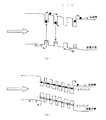
図5は、非特許文献1に記載された量子ドット太陽電池の構造を示し、図6は、そのエネルギバンド図を示す。図5に示すように、半導体基板100の裏面に裏面電極101が形成されており、半導体基板100上にn(n型半導体)層102が形成されている。そして、このn層102の上に、i(真性半導体)層103が形成されており、更に、このi層103の上に、p(p型半導体)層104が形成されている。このp層104の上に格子状のグリッド電極106が形成されており、このグリッド電極106の開口部に透明な反射防止膜105が形成されている。太陽光は、このグリッド電極106の開口部の反射防止膜105を透過してp層104、i層103及びn層102に入射する。
FIG. 5 shows the structure of the quantum dot solar cell described in Non-Patent Document 1, and FIG. 6 shows its energy band diagram. As shown in FIG. 5, a
i層103は、量子ドット層107と中間層108とを交互に積層したものであり、この量子ドット層107の間に挿入される中間層108の厚さが厚いと、エネルギバンド構造は、図6(a)に示すようになる。太陽光の吸収により励起された電子は、光励起又は熱励起により量子ドットの井戸から抜け出し、電流として取り出される。このとき、電子の非発光再結合及び発光再結合が生じ、エネルギの損失が生じる。
The i
一方、中間層の厚さを数nm程度まで薄くすると、図6(b)に示すように、量子ドット間にミニバンドが形成され、太陽光の吸収により励起した電子及び正孔は少ないエネルギ損失で移動することができ、このi層で生成する電流は多い。 On the other hand, when the thickness of the intermediate layer is reduced to about several nanometers, as shown in FIG. 6B, a miniband is formed between the quantum dots, and electrons and holes excited by absorption of sunlight are less energy loss. The current generated in this i layer is large.
上述のように、量子ドット層107によりi層103を構成することにより、ミニバンドが形成されるので、太陽光により電子及び正孔を励起するのに必要なエネルギは小さくてよく、少ない吸収エネルギで電子及び正孔を励起するので、効率よく電流が生成し、変換効率が高い。そして、励起した電子は、ミニバンドを伝導して、n層102に至る。
As described above, since the mini-band is formed by forming the
しかしながら、上述の如くして励起した電子は、n層102に移る際に、ミニバンドから伝導帯まで障壁を乗り越える必要がある。このため、従来の量子ドット太陽電池は、取り出せる電流に限界があった。
However, when the electrons excited as described above move to the
本発明はかかる問題点に鑑みてなされたものであって、i層にて太陽光により励起された電子又は正孔の流れを、n層又はp層に移行する際の障壁を小さくして、電流をミニバンドから取り出しやすくした太陽電池を提供することを目的とする。 The present invention has been made in view of such problems, and it is possible to reduce the barrier when transferring the flow of electrons or holes excited by sunlight in the i layer to the n layer or the p layer, An object is to provide a solar cell in which current can be easily taken out from a miniband.
本発明に係る太陽電池は、裏面電極と、この裏面電極上に形成されたn型半導体層と、このn型半導体層の上に形成された真性半導体層と、この真性半導体層の上に形成されたp型半導体層と、このp型半導体層の上に形成され太陽光を透過して前記真性半導体層に入射させる電極とを有し、前記真性半導体層並びに前記n型半導体層及びp型半導体層は、いずれも、量子ドット層であり、いずれも伝導帯及び荷電子帯よりも内側にミニバンドを有する層であることを特徴とする。 The solar cell according to the present invention includes a back electrode, an n-type semiconductor layer formed on the back electrode, an intrinsic semiconductor layer formed on the n-type semiconductor layer, and an intrinsic semiconductor layer. A p-type semiconductor layer formed on the p-type semiconductor layer, and an electrode that is formed on the p-type semiconductor layer and transmits sunlight to be incident on the intrinsic semiconductor layer. The intrinsic semiconductor layer, the n-type semiconductor layer, and the p-type semiconductor layer Each of the semiconductor layers is a quantum dot layer, and both are layers having a miniband inside the conduction band and the valence band.
本発明に係る他の太陽電池は、裏面電極と、この裏面電極上に形成されたn型半導体層と、このn型半導体層の上に形成された真性半導体層と、この真性半導体層の上に形成されたp型半導体層と、このp型半導体層の上に形成され太陽光を透過して前記真性半導体層に入射させる電極とを有し、前記真性半導体層並びに前記n型半導体層及びp型半導体層は、いずれも、粒子径が5乃至1000nmのナノ粒子からなる量子ドット層であり、いずれも伝導帯及び荷電子帯よりも内側にミニバンドを有する層であることを特徴とする。 Another solar cell according to the present invention includes a back electrode, an n-type semiconductor layer formed on the back electrode, an intrinsic semiconductor layer formed on the n-type semiconductor layer, and an upper surface of the intrinsic semiconductor layer. A p-type semiconductor layer formed on the p-type semiconductor layer, and an electrode that is formed on the p-type semiconductor layer and transmits sunlight to be incident on the intrinsic semiconductor layer. The intrinsic semiconductor layer, the n-type semiconductor layer, Each of the p-type semiconductor layers is a quantum dot layer made of nanoparticles having a particle diameter of 5 to 1000 nm, and both are layers having a miniband inside the conduction band and the valence band. .
この太陽電池において、例えば、前記真性半導体層は、Si粒子とAg粒子とが規則的に配置されたものであり、前記P型半導体層は、P型不純物をドープしたSi粒子と、Ag粒子とが規則的に配置されたものであり、前記N型半導体層は、N型不純物をドープしたSi粒子と、Ag粒子とが規則的に配置されたものである。 In this solar cell, for example, the intrinsic semiconductor layer is one in which Si particles and Ag particles are regularly arranged, and the P-type semiconductor layer includes Si particles doped with P-type impurities, Ag particles, Are regularly arranged, and the N-type semiconductor layer is one in which Si particles doped with N-type impurities and Ag particles are regularly arranged.
本発明によれば、n型半導体層(n層)及びp型半導体層(p層)も量子ドット層で構成するので、電子がi層からn層へ移行する際の障壁が小さく、大きな電流を高速で取り出すことができる。 According to the present invention, since the n-type semiconductor layer (n layer) and the p-type semiconductor layer (p layer) are also composed of quantum dot layers, the barrier when electrons move from the i layer to the n layer is small, and a large current Can be taken out at high speed.
以下、本発明の実施形態について、添付の図面を参照して具体的に説明する。図1は本発明の実施形態に係る太陽電池の薄膜構造を示す断面図、図2はそのエネルギバンドギャップ図である。図1に示すように、本実施形態の太陽電池は、裏面電極11の上には、n型半導体層(n層)12、真性半導体層(i層)13、p型半導体層(p層)14が積層されている。そして、p層14の上に格子状のグリッド電極16が形成されており、このグリッド電極16の開口部に反射防止膜15が形成されている。太陽光は、グリッド電極16の開口部の反射防止膜15を透過してp層14、i層13及びn層12に入射する。なお、反射防止膜15は太陽光が反射してしまうことを防止して効率よく太陽光を薄膜構造の中に取り込むための層である。また、n層12、i層13及びp層14の積層体にて励起した電子は、n層12から裏面電極11に流れる。一方、p層14からの正孔は、グリッド電極16に流れる。
Hereinafter, embodiments of the present invention will be specifically described with reference to the accompanying drawings. FIG. 1 is a cross-sectional view showing a thin film structure of a solar cell according to an embodiment of the present invention, and FIG. 2 is an energy band gap diagram thereof. As shown in FIG. 1, the solar cell of this embodiment has an n-type semiconductor layer (n layer) 12, an intrinsic semiconductor layer (i layer) 13, and a p-type semiconductor layer (p layer) on the
図3に示すように、例えば、i層13は、粒子径が5乃至1000nmの多数のシリコン(Si)粒子と、粒子径が5乃至1000nmのAg(銀)粒子とからなるベース構造を有し、これらのSi粒子とAg粒子とが規則的に配置されている。また、p層14は、同様に、粒子径が5乃至1000nmの多数のシリコン(Si)粒子と、粒子径が5乃至1000nmのAg(銀)粒子とが規則的に配置されているが、p層14においては、Si粒子にB(ボロン)等のp型不純物がドープされている。更に、n層12は、同様に、粒子径が5乃至1000nmの多数のシリコン(Si)粒子と、粒子径が5乃至1000nmのAg(銀)粒子とが規則的に配置されているが、n層12においては、Si粒子にAs(砒素)等のn型不純物がドープされている。なお、これらのドープ元素は、上記各元素に限らず、公知のp型ドープ元素及びn型ドープ元素を使用することができる。また、各ドープ元素の量を調整することにより、p層14及びn層12のフェルミ準位をコントロールすることができる。
As shown in FIG. 3, for example, the
ベース構造のAg粒子は、その間隔が一定になるように規則的に配列されている。次に、このベース構造の量子ドット層の形成方法の一例について、説明する。図3に示す粒子構造は、ナノ粒子のSi粒子が面心立方格子の格子点の位置に存在し、面心立方格子の一面において、その3軸が直交する位置にある4個のSi粒子が面心の位置にあるAg粒子に接触している。 The base-structured Ag particles are regularly arranged so that the intervals are constant. Next, an example of a method for forming the quantum dot layer having the base structure will be described. In the particle structure shown in FIG. 3, the nano-particle Si particles are present at the positions of the lattice points of the face-centered cubic lattice, and four Si particles having three axes orthogonal to each other on one surface of the face-centered cubic lattice. It is in contact with Ag particles at the face center position.
Ag粒子は、導電体粒子であり、ナノ粒子である。しかし、例えば、インジウム(In)、タンタル(Ta)、タングステン(W)等のレア・メタルのナノ粒子、金(Au)等の貴金属のナノ粒子も使用することもできる。インジウム、タンタル、タングステンは不定形であるが、市販のものの平均粒子径は、夫々25μm、0.8μm、0.6μmである。金及び銀は球状であるが、その市販のものの平均粒子径は0.5μm、0.2μmである。また、金(Au)のナノ粒子を溶液で供給する市販のAu粒子源としては、粒径が3.5〜5.5nm、3〜5nm及び2〜4nmのものがある。また、銀(Ag)のナノ粒子を溶液で供給する市販のAg粒子源としては、粒径が3〜7nm及び5〜15nmのものがある。 Ag particles are conductor particles and are nanoparticles. However, rare metal nanoparticles such as indium (In), tantalum (Ta), and tungsten (W), and noble metal nanoparticles such as gold (Au) can also be used. Indium, tantalum, and tungsten are amorphous, but the average particle diameters of commercially available products are 25 μm, 0.8 μm, and 0.6 μm, respectively. Gold and silver are spherical, but the average particle diameter of those commercially available is 0.5 μm and 0.2 μm. Also, commercially available Au particle sources that supply gold (Au) nanoparticles in solution include those with particle sizes of 3.5 to 5.5 nm, 3 to 5 nm, and 2 to 4 nm. In addition, commercially available Ag particle sources that supply silver (Ag) nanoparticles in a solution include those having a particle size of 3 to 7 nm and 5 to 15 nm.
この図3に示す粒子構造のベース構造は、以下のようにして形成することができる。図4に示すように、Ag粒子とSi粒子(真性半導体、p型半導体又はn型半導体のSi粒子)とを、均一に分散させた溶液6を、容器5内に貯留する。この溶液6の溶媒としては水を使用することができる。基板7は支持部材8に吊り下げられており、この支持部材8は昇降装置9により上下動可能になっている。そして、昇降装置9により支持部材8を介して基板7を下降させ、基板7を溶液6内に浸漬する。これにより、この基板7の表面に溶液6の層が付着する。そして、昇降装置9により、基板7を引き上げると、基板7の表面に付着した溶液6の層は、乾燥する過程で、表面張力により縮み、溶液内の粒子のうち、大径の粒子が最密充填の位置に位置して固化する。これにより、最密充填の結晶構造が面心立方格子の場合には、図3に示すように、大径のSi粒子が面心立方格子の格子点に位置し、面心位置にAg粒子が位置して、これらのSi粒子とAg粒子とが配置される。このような面心立方格子の結晶構造(粒子の配置構造)が3次元的に形成される。なお、基板7の引き上げ速度は、例えば、数百nm/s〜数十μm/sである。基板7の材質としては、ガラス、鉄板及びアルミニウムホイル等を使用することができ、更に、薄膜樹脂シート等も使用できる。
The base structure of the particle structure shown in FIG. 3 can be formed as follows. As shown in FIG. 4, a solution 6 in which Ag particles and Si particles (intrinsic semiconductor, p-type semiconductor, or n-type semiconductor Si particles) are uniformly dispersed is stored in a container 5. Water can be used as the solvent of the solution 6. The substrate 7 is suspended from a
このようにして、図3に示すように、面心立方格子の格子点の位置に大径のSi粒子が面心位置の小径のAg粒子に接触して存在し、これらのSi粒子とAg粒子とからなるナノ粒子の配置構造が得られる。このとき、Si粒子及びAg粒子の粒径が一定(均一)であると、約10nm以下の領域にAg粒子を配置し、電子をこの約10nmに閉じ込めることができる。なお、ナノ粒子の配置は、上記実施形態のように、面心立方格子の位置に限らず、種々の配置態様が考えられ、例えば、ナノ粒子を体心立方格子の位置に配置することもできる。 Thus, as shown in FIG. 3, large-diameter Si particles are present in contact with the small-diameter Ag particles at the face-centered position at the positions of the lattice points of the face-centered cubic lattice, and these Si particles and Ag particles A nanoparticle arrangement structure consisting of At this time, if the particle diameters of the Si particles and the Ag particles are constant (uniform), the Ag particles can be arranged in a region of about 10 nm or less, and the electrons can be confined to about 10 nm. The arrangement of the nanoparticles is not limited to the position of the face-centered cubic lattice as in the above embodiment, and various arrangement modes are conceivable. For example, the nanoparticles can be arranged at the position of the body-centered cubic lattice. .
このようにして、極めて容易に且つ高生産性で、量子ドットの半導体層を形成することができる。量子ドットは約10nm以下の領域に電子を閉じ込めることにより、半導体のバンドギャップを形成する技術である。これにより、図2に示すように、伝導帯及び荷電子帯よりも内側にミニバンドが形成され、光により励起された電子及び正孔がこのミニバンドを介して移動することができるようになる。 In this way, a semiconductor layer of quantum dots can be formed very easily and with high productivity. Quantum dots are a technique for forming a semiconductor band gap by confining electrons in a region of about 10 nm or less. Thereby, as shown in FIG. 2, a miniband is formed inside the conduction band and the valence band, and electrons and holes excited by light can move through the miniband. .
次に、上述のように構成された太陽電池の動作について説明する。p層14とn層12とのpn接合の間に、i層13を設けたので、太陽光は、pn接合の急峻なバンドエネルギ変化の伝導帯部分ではなく、緩やかなi層の伝導帯部分において、電子及び正孔を励起するため、効率的に電子及び正孔を励起することができ、太陽光の吸収効率が高い。そして、i層13で大量に生成した伝導帯の電子は、i層が量子ドット層であることから、そのミニバンドを経由して半導体基板10及び裏面電極11に向けて流れる。このため、電子及び正孔に対する太陽光の励起エネルギが低くても、電子及び正孔が十分に励起され、電流を取り出すことができる。
Next, the operation of the solar cell configured as described above will be described. Since the
一方、従来は、n層12及びp層14が夫々n型半導体層及びp型半導体層であったため、励起された電子がi層13からn層12に移行しようとするときに、図6(b)に示すように、n層12の伝導帯を乗り越える必要があり、この部分で、電子の流れが阻害されていた。また、正孔もp層14の荷電子帯を乗り越える必要があり、この部分で、正孔の流れが阻害されていた。
On the other hand, conventionally, since the
これに対し、本実施形態においては、p層14及びn層12も、量子ドット層で構成しているため、励起された電子は、n層12のミニバンドを伝導して、裏面電極11に到達するため、従来の障壁が解消され、電流を高効率で高速に取り出すことができる。正孔も同様に、p層14のミニバンドを伝導して、グリッド電極16に到達し、従来の障壁が障害となることなく、高効率でグリッド電極16に伝導する。
On the other hand, in this embodiment, since the
このようにして、本発明においては、n層及びp層として量子ドット層を形成したので、太陽電池により効率的に励起された電子を、高効率で取り出すことができ、大電流を高速で取り出すことができる。 Thus, in the present invention, since the quantum dot layers are formed as the n layer and the p layer, electrons efficiently excited by the solar cell can be extracted with high efficiency, and a large current can be extracted at high speed. be able to.
なお、本発明は上記実施形態に限定されるものではなく、例えば、p層14、i層13、n層12は、上記実施形態の図4に示すように、基板7を溶液6内に浸漬し、基板7の表面に溶液6の層を付着させ、溶液6の層が乾燥する過程で、表面張力により縮み、最密充填の結晶構造(面心立方格子)を形成することにより、量子ドット構造としたものではなく、例えば、エピタキシャル成長により、量子ドット構造を形成してもよい。量子ドットの構造自体は種々の方法で形成することができる。また、p層14、i層13、n層12の積層体は、適宜の半導体基板を支持体として形成してもよい。量子ドット層は、伝導帯及び荷電子帯よりも内側にミニバンドを有する層である。
In addition, this invention is not limited to the said embodiment, For example,
本発明は、太陽光を高効率で電気エネルギに変換する太陽電池のセルとして、大電流を高効率で高速に取り出すことができ、極めて有用である。 INDUSTRIAL APPLICABILITY The present invention is extremely useful as a solar battery cell that converts sunlight into electric energy with high efficiency and can extract a large current with high efficiency and at high speed.
6:溶液
7:基板
11、101:裏面電極
12:n層(量子ドット層)
13:i層(量子ドット層)
14:p層(量子ドット層)
15、105:反射防止膜
16、106:グリッド電極
102:n層
103:i層
104:p層
6: Solution 7:
13: i layer (quantum dot layer)
14: p layer (quantum dot layer)
15, 105:
Claims (3)
Priority Applications (1)
| Application Number | Priority Date | Filing Date | Title |
|---|---|---|---|
| JP2010136599A JP5586049B2 (en) | 2010-06-15 | 2010-06-15 | Solar cell |
Applications Claiming Priority (1)
| Application Number | Priority Date | Filing Date | Title |
|---|---|---|---|
| JP2010136599A JP5586049B2 (en) | 2010-06-15 | 2010-06-15 | Solar cell |
Publications (2)
| Publication Number | Publication Date |
|---|---|
| JP2012004251A true JP2012004251A (en) | 2012-01-05 |
| JP5586049B2 JP5586049B2 (en) | 2014-09-10 |
Family
ID=45535940
Family Applications (1)
| Application Number | Title | Priority Date | Filing Date |
|---|---|---|---|
| JP2010136599A Expired - Fee Related JP5586049B2 (en) | 2010-06-15 | 2010-06-15 | Solar cell |
Country Status (1)
| Country | Link |
|---|---|
| JP (1) | JP5586049B2 (en) |
Cited By (1)
| Publication number | Priority date | Publication date | Assignee | Title |
|---|---|---|---|---|
| JP2016127183A (en) * | 2015-01-06 | 2016-07-11 | シャープ株式会社 | Photoelectric conversion element |
Citations (3)
| Publication number | Priority date | Publication date | Assignee | Title |
|---|---|---|---|---|
| JP2009520358A (en) * | 2005-12-16 | 2009-05-21 | ザ トラスティーズ オブ プリンストン ユニヴァシティ | Intermediate band photosensitive device comprising quantum dots with tunnel barriers provided in an organic matrix |
| JP2010067803A (en) * | 2008-09-11 | 2010-03-25 | Seiko Epson Corp | Photoelectric conversion device, electronic apparatus, method for manufacturing photoelectric conversion device, and method for manufacturing electronic apparatus |
| WO2011004446A1 (en) * | 2009-07-06 | 2011-01-13 | トヨタ自動車株式会社 | Photoelectric conversion element |
-
2010
- 2010-06-15 JP JP2010136599A patent/JP5586049B2/en not_active Expired - Fee Related
Patent Citations (3)
| Publication number | Priority date | Publication date | Assignee | Title |
|---|---|---|---|---|
| JP2009520358A (en) * | 2005-12-16 | 2009-05-21 | ザ トラスティーズ オブ プリンストン ユニヴァシティ | Intermediate band photosensitive device comprising quantum dots with tunnel barriers provided in an organic matrix |
| JP2010067803A (en) * | 2008-09-11 | 2010-03-25 | Seiko Epson Corp | Photoelectric conversion device, electronic apparatus, method for manufacturing photoelectric conversion device, and method for manufacturing electronic apparatus |
| WO2011004446A1 (en) * | 2009-07-06 | 2011-01-13 | トヨタ自動車株式会社 | Photoelectric conversion element |
Cited By (1)
| Publication number | Priority date | Publication date | Assignee | Title |
|---|---|---|---|---|
| JP2016127183A (en) * | 2015-01-06 | 2016-07-11 | シャープ株式会社 | Photoelectric conversion element |
Also Published As
| Publication number | Publication date |
|---|---|
| JP5586049B2 (en) | 2014-09-10 |
Similar Documents
| Publication | Publication Date | Title |
|---|---|---|
| JP5035472B2 (en) | Photoelectric conversion element | |
| JP5077109B2 (en) | Photoelectric device | |
| JP5687765B2 (en) | Solar cell | |
| JP2013239690A (en) | Superlattice structure, semiconductor device and semiconductor light emitting device including the superlattice structure, and method of making the superlattice structure | |
| TW200849613A (en) | Photovoltaic cell with reduced hot-carrier cooling | |
| TW200845404A (en) | Photovoltaic cell and method of making thereof | |
| JP2006261666A (en) | Efficient inorganic nano rod reinforcement light electromotive element | |
| TW201001726A (en) | Techniques for enhancing efficiency of photovoltaic devices using high-aspect-ratio nanostructures | |
| KR101264880B1 (en) | Silicon Solar Cell and Manufacturing Method thereof | |
| Hong et al. | Nanostructuring methods for enhancing light absorption rate of Si-based photovoltaic devices: A review | |
| JP2011138804A (en) | Nanowire solar cell and method of manufacturing the same | |
| Das et al. | SnS2/Si nanowire vertical heterostructure for high performance ultra-low power broadband photodetector with excellent detectivity | |
| TW201314931A (en) | Charge-coupled photovoltaic devices | |
| US20140116502A1 (en) | Quantum nanodots, two-dimensional quantum nanodot array as well as semiconductor device using the same and production method therefor | |
| JP2011100779A (en) | Semiconductor device and method of manufacturing the same | |
| JP5586049B2 (en) | Solar cell | |
| Fallahazad et al. | Porous pyramidal silicon structures for improved light sensing performance | |
| JP5540263B2 (en) | Semiconductor device and manufacturing method thereof | |
| Pylypova et al. | Influence of Si Nanowires Parameters and Ag Nanoparticles on Light Trapping in Solar Cells | |
| JP2011029464A (en) | Quantum dot solar cell | |
| Kushwaha et al. | Roughness enhanced surface defects and photoconductivity of acid etched ZnO nanowires | |
| JP6121757B2 (en) | Solar cell | |
| JP6336731B2 (en) | Solar cell | |
| JP2013106025A (en) | Photoelectric conversion element | |
| JP2014146701A (en) | Quantum dot and solar cell |
Legal Events
| Date | Code | Title | Description |
|---|---|---|---|
| A621 | Written request for application examination |
Free format text: JAPANESE INTERMEDIATE CODE: A621 Effective date: 20130514 |
|
| A131 | Notification of reasons for refusal |
Free format text: JAPANESE INTERMEDIATE CODE: A131 Effective date: 20140415 |
|
| A521 | Request for written amendment filed |
Free format text: JAPANESE INTERMEDIATE CODE: A523 Effective date: 20140610 |
|
| TRDD | Decision of grant or rejection written | ||
| A01 | Written decision to grant a patent or to grant a registration (utility model) |
Free format text: JAPANESE INTERMEDIATE CODE: A01 Effective date: 20140701 |
|
| A61 | First payment of annual fees (during grant procedure) |
Free format text: JAPANESE INTERMEDIATE CODE: A61 Effective date: 20140717 |
|
| R150 | Certificate of patent or registration of utility model |
Ref document number: 5586049 Country of ref document: JP Free format text: JAPANESE INTERMEDIATE CODE: R150 |
|
| R250 | Receipt of annual fees |
Free format text: JAPANESE INTERMEDIATE CODE: R250 |
|
| LAPS | Cancellation because of no payment of annual fees |