JP2011523200A - Nanowire wrap gate device - Google Patents
Nanowire wrap gate device Download PDFInfo
- Publication number
- JP2011523200A JP2011523200A JP2011504964A JP2011504964A JP2011523200A JP 2011523200 A JP2011523200 A JP 2011523200A JP 2011504964 A JP2011504964 A JP 2011504964A JP 2011504964 A JP2011504964 A JP 2011504964A JP 2011523200 A JP2011523200 A JP 2011523200A
- Authority
- JP
- Japan
- Prior art keywords
- region
- nanowire
- semiconductor device
- gate electrode
- wrap gate
- Prior art date
- Legal status (The legal status is an assumption and is not a legal conclusion. Google has not performed a legal analysis and makes no representation as to the accuracy of the status listed.)
- Pending
Links
- 239000002070 nanowire Substances 0.000 title claims abstract description 195
- 239000004065 semiconductor Substances 0.000 claims abstract description 81
- 239000002800 charge carrier Substances 0.000 claims abstract description 46
- 239000000463 material Substances 0.000 claims description 19
- 239000000203 mixture Substances 0.000 claims description 16
- 230000008859 change Effects 0.000 claims description 12
- 230000005294 ferromagnetic effect Effects 0.000 claims description 10
- 238000000034 method Methods 0.000 claims description 10
- 239000000758 substrate Substances 0.000 claims description 9
- 230000005307 ferromagnetism Effects 0.000 claims description 2
- 238000010586 diagram Methods 0.000 description 12
- 239000002019 doping agent Substances 0.000 description 8
- 238000006243 chemical reaction Methods 0.000 description 6
- 238000005516 engineering process Methods 0.000 description 6
- 230000000694 effects Effects 0.000 description 5
- 230000005669 field effect Effects 0.000 description 5
- 230000004913 activation Effects 0.000 description 4
- 238000002513 implantation Methods 0.000 description 4
- 230000005291 magnetic effect Effects 0.000 description 4
- 239000002245 particle Substances 0.000 description 4
- 230000006798 recombination Effects 0.000 description 4
- 238000005215 recombination Methods 0.000 description 4
- 230000008901 benefit Effects 0.000 description 3
- 239000003054 catalyst Substances 0.000 description 3
- 238000001816 cooling Methods 0.000 description 3
- 239000002096 quantum dot Substances 0.000 description 3
- 229910000980 Aluminium gallium arsenide Inorganic materials 0.000 description 2
- 229910001218 Gallium arsenide Inorganic materials 0.000 description 2
- 239000000969 carrier Substances 0.000 description 2
- 230000008878 coupling Effects 0.000 description 2
- 238000010168 coupling process Methods 0.000 description 2
- 238000005859 coupling reaction Methods 0.000 description 2
- 238000009792 diffusion process Methods 0.000 description 2
- 230000006870 function Effects 0.000 description 2
- 239000012535 impurity Substances 0.000 description 2
- 230000006698 induction Effects 0.000 description 2
- 239000007788 liquid Substances 0.000 description 2
- 238000004519 manufacturing process Methods 0.000 description 2
- 230000007246 mechanism Effects 0.000 description 2
- 239000002086 nanomaterial Substances 0.000 description 2
- 239000007790 solid phase Substances 0.000 description 2
- 238000003860 storage Methods 0.000 description 2
- 230000003213 activating effect Effects 0.000 description 1
- 238000003491 array Methods 0.000 description 1
- 230000003190 augmentative effect Effects 0.000 description 1
- 230000004888 barrier function Effects 0.000 description 1
- 230000015572 biosynthetic process Effects 0.000 description 1
- 238000004871 chemical beam epitaxy Methods 0.000 description 1
- 238000010276 construction Methods 0.000 description 1
- 230000001419 dependent effect Effects 0.000 description 1
- 238000009826 distribution Methods 0.000 description 1
- 230000005684 electric field Effects 0.000 description 1
- 230000005284 excitation Effects 0.000 description 1
- 239000003302 ferromagnetic material Substances 0.000 description 1
- 238000010438 heat treatment Methods 0.000 description 1
- 230000007774 longterm Effects 0.000 description 1
- 230000001404 mediated effect Effects 0.000 description 1
- 230000004048 modification Effects 0.000 description 1
- 238000012986 modification Methods 0.000 description 1
- 239000002073 nanorod Substances 0.000 description 1
- 239000002071 nanotube Substances 0.000 description 1
- 150000004767 nitrides Chemical class 0.000 description 1
- 239000012071 phase Substances 0.000 description 1
- 238000010248 power generation Methods 0.000 description 1
- 230000008569 process Effects 0.000 description 1
- 238000001228 spectrum Methods 0.000 description 1
- 230000005676 thermoelectric effect Effects 0.000 description 1
- 238000000927 vapour-phase epitaxy Methods 0.000 description 1
Images


Classifications
-
- H—ELECTRICITY
- H01—ELECTRIC ELEMENTS
- H01L—SEMICONDUCTOR DEVICES NOT COVERED BY CLASS H10
- H01L29/00—Semiconductor devices specially adapted for rectifying, amplifying, oscillating or switching and having potential barriers; Capacitors or resistors having potential barriers, e.g. a PN-junction depletion layer or carrier concentration layer; Details of semiconductor bodies or of electrodes thereof ; Multistep manufacturing processes therefor
- H01L29/02—Semiconductor bodies ; Multistep manufacturing processes therefor
- H01L29/06—Semiconductor bodies ; Multistep manufacturing processes therefor characterised by their shape; characterised by the shapes, relative sizes, or dispositions of the semiconductor regions ; characterised by the concentration or distribution of impurities within semiconductor regions
- H01L29/0657—Semiconductor bodies ; Multistep manufacturing processes therefor characterised by their shape; characterised by the shapes, relative sizes, or dispositions of the semiconductor regions ; characterised by the concentration or distribution of impurities within semiconductor regions characterised by the shape of the body
- H01L29/0665—Semiconductor bodies ; Multistep manufacturing processes therefor characterised by their shape; characterised by the shapes, relative sizes, or dispositions of the semiconductor regions ; characterised by the concentration or distribution of impurities within semiconductor regions characterised by the shape of the body the shape of the body defining a nanostructure
-
- B—PERFORMING OPERATIONS; TRANSPORTING
- B82—NANOTECHNOLOGY
- B82Y—SPECIFIC USES OR APPLICATIONS OF NANOSTRUCTURES; MEASUREMENT OR ANALYSIS OF NANOSTRUCTURES; MANUFACTURE OR TREATMENT OF NANOSTRUCTURES
- B82Y10/00—Nanotechnology for information processing, storage or transmission, e.g. quantum computing or single electron logic
-
- H—ELECTRICITY
- H01—ELECTRIC ELEMENTS
- H01L—SEMICONDUCTOR DEVICES NOT COVERED BY CLASS H10
- H01L29/00—Semiconductor devices specially adapted for rectifying, amplifying, oscillating or switching and having potential barriers; Capacitors or resistors having potential barriers, e.g. a PN-junction depletion layer or carrier concentration layer; Details of semiconductor bodies or of electrodes thereof ; Multistep manufacturing processes therefor
- H01L29/02—Semiconductor bodies ; Multistep manufacturing processes therefor
- H01L29/06—Semiconductor bodies ; Multistep manufacturing processes therefor characterised by their shape; characterised by the shapes, relative sizes, or dispositions of the semiconductor regions ; characterised by the concentration or distribution of impurities within semiconductor regions
- H01L29/0657—Semiconductor bodies ; Multistep manufacturing processes therefor characterised by their shape; characterised by the shapes, relative sizes, or dispositions of the semiconductor regions ; characterised by the concentration or distribution of impurities within semiconductor regions characterised by the shape of the body
- H01L29/0665—Semiconductor bodies ; Multistep manufacturing processes therefor characterised by their shape; characterised by the shapes, relative sizes, or dispositions of the semiconductor regions ; characterised by the concentration or distribution of impurities within semiconductor regions characterised by the shape of the body the shape of the body defining a nanostructure
- H01L29/0669—Nanowires or nanotubes
- H01L29/0673—Nanowires or nanotubes oriented parallel to a substrate
-
- H—ELECTRICITY
- H01—ELECTRIC ELEMENTS
- H01L—SEMICONDUCTOR DEVICES NOT COVERED BY CLASS H10
- H01L29/00—Semiconductor devices specially adapted for rectifying, amplifying, oscillating or switching and having potential barriers; Capacitors or resistors having potential barriers, e.g. a PN-junction depletion layer or carrier concentration layer; Details of semiconductor bodies or of electrodes thereof ; Multistep manufacturing processes therefor
- H01L29/02—Semiconductor bodies ; Multistep manufacturing processes therefor
- H01L29/06—Semiconductor bodies ; Multistep manufacturing processes therefor characterised by their shape; characterised by the shapes, relative sizes, or dispositions of the semiconductor regions ; characterised by the concentration or distribution of impurities within semiconductor regions
- H01L29/0657—Semiconductor bodies ; Multistep manufacturing processes therefor characterised by their shape; characterised by the shapes, relative sizes, or dispositions of the semiconductor regions ; characterised by the concentration or distribution of impurities within semiconductor regions characterised by the shape of the body
- H01L29/0665—Semiconductor bodies ; Multistep manufacturing processes therefor characterised by their shape; characterised by the shapes, relative sizes, or dispositions of the semiconductor regions ; characterised by the concentration or distribution of impurities within semiconductor regions characterised by the shape of the body the shape of the body defining a nanostructure
- H01L29/0669—Nanowires or nanotubes
- H01L29/0676—Nanowires or nanotubes oriented perpendicular or at an angle to a substrate
-
- H—ELECTRICITY
- H01—ELECTRIC ELEMENTS
- H01L—SEMICONDUCTOR DEVICES NOT COVERED BY CLASS H10
- H01L29/00—Semiconductor devices specially adapted for rectifying, amplifying, oscillating or switching and having potential barriers; Capacitors or resistors having potential barriers, e.g. a PN-junction depletion layer or carrier concentration layer; Details of semiconductor bodies or of electrodes thereof ; Multistep manufacturing processes therefor
- H01L29/02—Semiconductor bodies ; Multistep manufacturing processes therefor
- H01L29/06—Semiconductor bodies ; Multistep manufacturing processes therefor characterised by their shape; characterised by the shapes, relative sizes, or dispositions of the semiconductor regions ; characterised by the concentration or distribution of impurities within semiconductor regions
- H01L29/0657—Semiconductor bodies ; Multistep manufacturing processes therefor characterised by their shape; characterised by the shapes, relative sizes, or dispositions of the semiconductor regions ; characterised by the concentration or distribution of impurities within semiconductor regions characterised by the shape of the body
- H01L29/0665—Semiconductor bodies ; Multistep manufacturing processes therefor characterised by their shape; characterised by the shapes, relative sizes, or dispositions of the semiconductor regions ; characterised by the concentration or distribution of impurities within semiconductor regions characterised by the shape of the body the shape of the body defining a nanostructure
- H01L29/0669—Nanowires or nanotubes
- H01L29/068—Nanowires or nanotubes comprising a junction
-
- H—ELECTRICITY
- H01—ELECTRIC ELEMENTS
- H01L—SEMICONDUCTOR DEVICES NOT COVERED BY CLASS H10
- H01L29/00—Semiconductor devices specially adapted for rectifying, amplifying, oscillating or switching and having potential barriers; Capacitors or resistors having potential barriers, e.g. a PN-junction depletion layer or carrier concentration layer; Details of semiconductor bodies or of electrodes thereof ; Multistep manufacturing processes therefor
- H01L29/40—Electrodes ; Multistep manufacturing processes therefor
- H01L29/41—Electrodes ; Multistep manufacturing processes therefor characterised by their shape, relative sizes or dispositions
- H01L29/423—Electrodes ; Multistep manufacturing processes therefor characterised by their shape, relative sizes or dispositions not carrying the current to be rectified, amplified or switched
- H01L29/42312—Gate electrodes for field effect devices
- H01L29/42316—Gate electrodes for field effect devices for field-effect transistors
- H01L29/4232—Gate electrodes for field effect devices for field-effect transistors with insulated gate
- H01L29/42372—Gate electrodes for field effect devices for field-effect transistors with insulated gate characterised by the conducting layer, e.g. the length, the sectional shape or the lay-out
- H01L29/42376—Gate electrodes for field effect devices for field-effect transistors with insulated gate characterised by the conducting layer, e.g. the length, the sectional shape or the lay-out characterised by the length or the sectional shape
-
- H—ELECTRICITY
- H01—ELECTRIC ELEMENTS
- H01L—SEMICONDUCTOR DEVICES NOT COVERED BY CLASS H10
- H01L29/00—Semiconductor devices specially adapted for rectifying, amplifying, oscillating or switching and having potential barriers; Capacitors or resistors having potential barriers, e.g. a PN-junction depletion layer or carrier concentration layer; Details of semiconductor bodies or of electrodes thereof ; Multistep manufacturing processes therefor
- H01L29/66—Types of semiconductor device ; Multistep manufacturing processes therefor
- H01L29/68—Types of semiconductor device ; Multistep manufacturing processes therefor controllable by only the electric current supplied, or only the electric potential applied, to an electrode which does not carry the current to be rectified, amplified or switched
- H01L29/70—Bipolar devices
- H01L29/72—Transistor-type devices, i.e. able to continuously respond to applied control signals
- H01L29/739—Transistor-type devices, i.e. able to continuously respond to applied control signals controlled by field-effect, e.g. bipolar static induction transistors [BSIT]
- H01L29/7391—Gated diode structures
-
- H—ELECTRICITY
- H01—ELECTRIC ELEMENTS
- H01L—SEMICONDUCTOR DEVICES NOT COVERED BY CLASS H10
- H01L29/00—Semiconductor devices specially adapted for rectifying, amplifying, oscillating or switching and having potential barriers; Capacitors or resistors having potential barriers, e.g. a PN-junction depletion layer or carrier concentration layer; Details of semiconductor bodies or of electrodes thereof ; Multistep manufacturing processes therefor
- H01L29/66—Types of semiconductor device ; Multistep manufacturing processes therefor
- H01L29/68—Types of semiconductor device ; Multistep manufacturing processes therefor controllable by only the electric current supplied, or only the electric potential applied, to an electrode which does not carry the current to be rectified, amplified or switched
- H01L29/76—Unipolar devices, e.g. field effect transistors
- H01L29/772—Field effect transistors
- H01L29/775—Field effect transistors with one dimensional charge carrier gas channel, e.g. quantum wire FET
-
- H—ELECTRICITY
- H01—ELECTRIC ELEMENTS
- H01L—SEMICONDUCTOR DEVICES NOT COVERED BY CLASS H10
- H01L33/00—Semiconductor devices having potential barriers specially adapted for light emission; Processes or apparatus specially adapted for the manufacture or treatment thereof or of parts thereof; Details thereof
- H01L33/0004—Devices characterised by their operation
- H01L33/0041—Devices characterised by their operation characterised by field-effect operation
-
- H—ELECTRICITY
- H01—ELECTRIC ELEMENTS
- H01L—SEMICONDUCTOR DEVICES NOT COVERED BY CLASS H10
- H01L33/00—Semiconductor devices having potential barriers specially adapted for light emission; Processes or apparatus specially adapted for the manufacture or treatment thereof or of parts thereof; Details thereof
- H01L33/02—Semiconductor devices having potential barriers specially adapted for light emission; Processes or apparatus specially adapted for the manufacture or treatment thereof or of parts thereof; Details thereof characterised by the semiconductor bodies
- H01L33/16—Semiconductor devices having potential barriers specially adapted for light emission; Processes or apparatus specially adapted for the manufacture or treatment thereof or of parts thereof; Details thereof characterised by the semiconductor bodies with a particular crystal structure or orientation, e.g. polycrystalline, amorphous or porous
- H01L33/18—Semiconductor devices having potential barriers specially adapted for light emission; Processes or apparatus specially adapted for the manufacture or treatment thereof or of parts thereof; Details thereof characterised by the semiconductor bodies with a particular crystal structure or orientation, e.g. polycrystalline, amorphous or porous within the light emitting region
Landscapes
- Engineering & Computer Science (AREA)
- Power Engineering (AREA)
- Microelectronics & Electronic Packaging (AREA)
- Computer Hardware Design (AREA)
- Nanotechnology (AREA)
- Chemical & Material Sciences (AREA)
- Physics & Mathematics (AREA)
- Ceramic Engineering (AREA)
- Condensed Matter Physics & Semiconductors (AREA)
- General Physics & Mathematics (AREA)
- Crystallography & Structural Chemistry (AREA)
- Materials Engineering (AREA)
- Manufacturing & Machinery (AREA)
- Mathematical Physics (AREA)
- Theoretical Computer Science (AREA)
- Thin Film Transistor (AREA)
- Insulated Gate Type Field-Effect Transistor (AREA)
Abstract
本発明は、第1の導電型の第1の縦方向領域(121)と、第2の導電型の第2の縦方向領域(122)と、第1の半導体ナノワイヤ(105)の前記第1の領域(121)に配置された少なくとも第1のラップゲート電極(111)とを含み、電圧が前記第1のラップゲート電極(111)に印加された場合に前記第1の縦方向領域(121)において電荷キャリア濃度を変更する少なくとも第1の半導体ナノワイヤ(105)を備えた半導体デバイスを提供する。第2のラップゲート電極(112)は、第2の縦方向領域(122)に配置されるのが好ましい。これにより、調整可能な擬似的な接合(114)がナノワイヤ(105)の実質的なドーピングなしで達成される。
【選択図】図2BThe present invention provides a first longitudinal region (121) of a first conductivity type, a second longitudinal region (122) of a second conductivity type, and the first of a first semiconductor nanowire (105). At least a first wrap gate electrode (111) disposed in the first wrap gate electrode (111), and when the voltage is applied to the first wrap gate electrode (111), the first vertical region (121) ) To provide a semiconductor device comprising at least a first semiconductor nanowire (105) that changes the charge carrier concentration. The second wrap gate electrode (112) is preferably disposed in the second longitudinal region (122). Thereby, an adjustable pseudo junction (114) is achieved without substantial doping of the nanowire (105).
[Selection] Figure 2B
Description
本発明は、一般には、ナノワイヤを用いた半導体デバイスに関し、特に、バンドギャップ、電荷キャリア型、電荷キャリア濃度、強磁性特性等に関して高精度特性を要求するナノワイヤを用いた半導体デバイスに関する。 The present invention generally relates to a semiconductor device using nanowires, and more particularly to a semiconductor device using nanowires that require high-precision characteristics with respect to band gap, charge carrier type, charge carrier concentration, ferromagnetic characteristics, and the like.
以下に更に説明するように、半導体デバイスは、最近まで、小型化及び最適な材料の選択に関して制約を与えるプレーナ技術に基づいていた。ナノテクノロジーの発展、及び、特に、ナノワイヤを生成する新しい技術により、プレーナ技術では不可能であった、改善された特性を有する半導体デバイスを設計し、且つ、新しいデバイスを作成する新しい可能性が得られた。このような半導体デバイスは、ナノワイヤ固有の特性、2次元、1次元又は0次元の量子閉じ込め、格子整合性の制約が軽減されたことによる軸方向の材料不均一性の適応性、アンテナ特性、バリスティック輸送、導波特性等から利点が得られる。 As will be described further below, semiconductor devices have until recently been based on planar technology that constrains miniaturization and optimal material selection. Advances in nanotechnology, and in particular, new technologies for generating nanowires, offer new possibilities for designing and creating new devices with improved properties that were not possible with planar technology. It was. Such semiconductor devices have characteristics inherent to nanowires, two-dimensional, one-dimensional, or zero-dimensional quantum confinement, axial material non-uniformity due to reduced constraints on lattice matching, antenna characteristics, variability. Advantages are obtained from stick transport, waveguide characteristics, and the like.
しかしながら、電界効果トランジスタ、発光ダイオード、半導体レーザ及びセンサ等の半導体デバイスをナノワイヤから製造するために、ナノワイヤにおいて注入領域(doped regions)を形成できることは非常に重要である。これは、いくつかの半導体デバイスの重要な部分である構造、即ち、基本的なpn接合を考慮すると理解される。ここで、ビルトイン電圧は、互いに隣接するp注入領域及びn注入領域を形成することにより得られる。ナノワイヤを用いた半導体デバイスにおいて、ナノワイヤの長さに沿ったpn接合は、異なる組成及び/又はドーピングの縦方向セグメントを形成することにより提供される。この種のナノワイヤに沿ったバンドギャップの調整は、例えば、異なるバンドギャップ及び/又はドーピングレベルの縦方向セグメントを使用することにより、ナノワイヤを用いた電界効果トランジスタのソース/ゲート間及びゲート/ドレイン間のアクセス抵抗を低減するために使用可能である。一般に、バンドギャップは、異なるバンドギャップを有する種々の半導体材料の縦方向セグメントを含むヘテロ構造を使用することにより変更される。更に、ドーパントの種類及びドーピングレベルは、ナノワイヤの成長中又は成長後に長さに沿って変動する。成長中、ドーパントは気相で注入され、成長後、ドーパントは拡散によりナノワイヤに注入される、或いは、電荷キャリア濃度は周囲の層からのいわゆる変調ドーピングにより影響を受ける。 However, in order to manufacture semiconductor devices such as field effect transistors, light emitting diodes, semiconductor lasers and sensors from nanowires, it is very important to be able to form doped regions in the nanowires. This is understood when considering the structure that is an important part of some semiconductor devices, namely the basic pn junction. Here, the built-in voltage is obtained by forming a p implantation region and an n implantation region adjacent to each other. In semiconductor devices using nanowires, pn junctions along the length of the nanowire are provided by forming longitudinal segments of different composition and / or doping. The adjustment of the band gap along this type of nanowire can be achieved, for example, by using longitudinal segments with different band gaps and / or doping levels, between source / gate and gate / drain of field effect transistors using nanowires. Can be used to reduce the access resistance. In general, the band gap is altered by using heterostructures that include longitudinal segments of various semiconductor materials having different band gaps. Further, the dopant type and doping level varies along the length during or after nanowire growth. During growth, the dopant is implanted in the gas phase and after growth, the dopant is implanted into the nanowire by diffusion, or the charge carrier concentration is affected by so-called modulated doping from the surrounding layers.
米国特許第5,362,972号において、ラップゲート電界効果トランジスタが開示されている。ラップゲート電界効果トランジスタは、一部分がゲートにより取り囲まれる又は覆われるナノワイヤを含む。ナノワイヤは、トランジスタの電流チャネルとして動作し、ゲートにより生成された電界は、トランジスタの動作のために、即ち、電流チャネルに沿って電荷キャリアの流れを制御するために使用される。ナノワイヤのドーピングにより、nチャネル、pチャネル、増加型又は空乏型トランジスタが形成されることが国際公開第2008/034850号から理解される。国際公開第2006/135336号において、ヘテロ構造セグメントは、電流制御、閾値電圧制御及び電流オンオフ比等の特性を向上するために、ラップゲート電界効果トランジスタのナノワイヤに更に導入される。 In US Pat. No. 5,362,972, a wrap gate field effect transistor is disclosed. Wrapped gate field effect transistors include nanowires that are partially surrounded or covered by a gate. The nanowire operates as the current channel of the transistor, and the electric field generated by the gate is used for the operation of the transistor, i.e. to control the flow of charge carriers along the current channel. It is understood from WO 2008/034850 that n-channel, p-channel, augmented or depleted transistors are formed by doping nanowires. In WO 2006/135336, heterostructure segments are further introduced into the wrap gate field effect transistor nanowires to improve properties such as current control, threshold voltage control and current on / off ratio.
ナノワイヤのドーピングは、いくつかの原因により困難である。例えば、結晶ナノワイヤへのドーパントの物理的な注入は禁止されている可能性があり、特定のドーパント濃度から得られた電荷キャリア濃度は、対応するバルク半導体材料のドーピングから予想したものより低い。例えば、いわゆるVLS(気相−液相−固相)機構を使用して触媒粒子から成長するナノワイヤの場合、触媒粒子におけるドーパントの溶解度及び拡散は、ドーパントの注入に影響を及ぼす。一般に、ナノワイヤに対する同様の長期結果を有する1つの関連した効果は、表面サイトに対するナノワイヤにおけるドーパントの外方拡散である。この効果は、ナノワイヤの高い表面対体積比により向上される。キャリアリザーバの体積を減少させる表面空乏効果は、ナノワイヤの高い表面対体積比のために増加される。 Nanowire doping is difficult for several reasons. For example, physical implantation of dopants into crystalline nanowires may be prohibited, and the charge carrier concentration obtained from a particular dopant concentration is lower than expected from the corresponding bulk semiconductor material doping. For example, in the case of nanowires grown from catalyst particles using the so-called VLS (gas phase-liquid phase-solid phase) mechanism, the solubility and diffusion of the dopant in the catalyst particles affects the implantation of the dopant. In general, one related effect with similar long term results for nanowires is outdiffusion of dopants in the nanowires to surface sites. This effect is enhanced by the high surface to volume ratio of the nanowire. The surface depletion effect that reduces the volume of the carrier reservoir is increased due to the high surface to volume ratio of the nanowires.
上記を考慮すると、本発明の目的は、ナノワイヤのドーピングに関連した特性に関してナノワイヤを含む半導体デバイスを改善することである。これは、独立請求項で規定される半導体デバイス及び方法により達成される。 In view of the above, it is an object of the present invention to improve semiconductor devices comprising nanowires with respect to properties associated with nanowire doping. This is achieved by a semiconductor device and method as defined in the independent claims.
本発明の第1の側面において、少なくとも第1の半導体ナノワイヤを備えた半導体デバイスが提供される。ナノワイヤは、第1の導電型の第1の縦方向領域と、第2の導電型の第2の縦方向領域と、前記第1の領域に配置された少なくとも第1のラップゲート電極とを有する。前記ラップゲート電極は、電圧が第1のラップゲート電極に印加された時に、第1の縦方向領域と関連付けられたナノワイヤの少なくとも第1の部分において電荷キャリア濃度を変更するように構成される。 In a first aspect of the present invention, a semiconductor device comprising at least a first semiconductor nanowire is provided. The nanowire has a first vertical region of a first conductivity type, a second vertical region of a second conductivity type, and at least a first wrap gate electrode disposed in the first region. . The wrap gate electrode is configured to change the charge carrier concentration in at least a first portion of the nanowire associated with the first longitudinal region when a voltage is applied to the first wrap gate electrode.
第2の縦方向領域は、第1のナノワイヤと電気的に接続される第2のナノワイヤ又はナノワイヤの長さに沿って第1の縦方向領域と一列に配置されてもよい。追加のラップゲートは、ナノワイヤの長さに沿って電荷キャリア濃度を変更するために第2の縦方向領域又は他の領域に配置される。 The second longitudinal region may be aligned with the first longitudinal region along the length of the second nanowire or nanowire that is electrically connected to the first nanowire. An additional wrap gate is placed in the second longitudinal region or other region to change the charge carrier concentration along the length of the nanowire.
半導体デバイスの第1のナノワイヤは、コアと、径方向のヘテロ構造を形成する少なくとも第1のシェル層とを含んでもよく、ヘテロ構造は、光を生成するために使用されてもよい。 The first nanowire of the semiconductor device may include a core and at least a first shell layer that forms a radial heterostructure, which may be used to generate light.
本発明の一実施形態において、半導体デバイスは熱電素子として動作するように構成される。 In one embodiment of the present invention, the semiconductor device is configured to operate as a thermoelectric element.
本発明の第2の側面において、半導体デバイスが、例えば、メモリ素子として動作するように、強磁性体を含むナノワイヤを含む半導体デバイスが提供される。これは、強磁性体の強磁性特性が変更されるように電荷キャリア濃度を変更するためにナノワイヤの領域に配置されたラップゲート電極に電圧を印加することにより達成される。 In a second aspect of the present invention, there is provided a semiconductor device comprising nanowires comprising a ferromagnetic material such that the semiconductor device operates as a memory element, for example. This is achieved by applying a voltage to the wrap gate electrode located in the nanowire region to change the charge carrier concentration so that the ferromagnetic properties of the ferromagnet are changed.
本発明によれば、特に、局所的ゲート制御及び反転により半導体デバイス及びナノワイヤを用いた半導体デバイスの従来のドーピングを置換できる、或いは、実質的なドーッピングを回避できる。一例として、本発明によれば、従来のデバイス及び波長調整可能なLED(発光ダイオード)等の調整可能な半導体デバイスのように空乏領域に空間電荷を有することなく改善されたpn接合の形成が可能となる。 In accordance with the present invention, conventional doping of semiconductor devices using semiconductor devices and nanowires can be replaced by local gate control and inversion, or substantial doping can be avoided. As an example, according to the present invention, an improved pn junction can be formed without having a space charge in a depletion region like conventional devices and tunable semiconductor devices such as wavelength tunable LEDs (light emitting diodes). It becomes.
本発明の実施形態は、従属請求項で規定される。添付の図面及び請求項を考慮して、本発明の他の目的、利点及び新しい特徴は、本発明の以下の詳細な説明で明らかとなるだろう。 Embodiments of the invention are defined in the dependent claims. Other objects, advantages and novel features of the invention will become apparent from the following detailed description of the invention when considered in conjunction with the accompanying drawings and claims.
添付の図面を参照して本発明の好適な実施形態を説明する。
本発明の実施形態は、いわゆるナノワイヤを含むナノ構造に基づいている。本出願の目的のために、ナノワイヤは、ナノメートルの寸法の幅及び直径を有し、且つ、典型的には、1次元特性を提供する縦長の形状を有するものと解釈される。このような構造は、一般に、ナノウィスカ、ナノロッド、ナノチューブ、1次元ナノ素子とも呼ばれる。粒子支援成長又は米国特許第7,335,908号に説明されているいわゆるVLS(気相−液相−固相)機構により基板上にナノワイヤを形成する基本的な処理、種々の化学ビームエピタキシー法及び気相エピタキシー法が知られている。但し、本発明は、このようなナノワイヤにもVLS法にも限定されない。ナノワイヤを成長させる他の適切な方法は、当業界で知られており、例えば、国際公開第2007/104784号において示されている。これによると、ナノワイヤは、粒子を触媒として使用せずに成長させられる。従って、選択的に成長されたナノワイヤ及びナノ構造、エッチングされた構造、他のナノワイヤ、及び、ナノワイヤから製造された構造が更に含まれる。 Embodiments of the invention are based on nanostructures comprising so-called nanowires. For purposes of this application, nanowires are interpreted as having a width and diameter of nanometer dimensions and typically having an elongated shape that provides one-dimensional properties. Such a structure is generally called a nanowhisker, nanorod, nanotube, or one-dimensional nanodevice. Basic process for forming nanowires on a substrate by means of particle assisted growth or the so-called VLS (gas phase-liquid phase-solid phase) mechanism described in US Pat. No. 7,335,908, various chemical beam epitaxy methods And vapor phase epitaxy is known. However, the present invention is not limited to such nanowires or VLS methods. Other suitable methods for growing nanowires are known in the art and are shown, for example, in WO 2007/104784. According to this, nanowires can be grown without using particles as a catalyst. Thus, selectively grown nanowires and nanostructures, etched structures, other nanowires, and structures made from nanowires are further included.
ナノワイヤは、必ずしもその長さに沿って均一であるとは限らない。ナノメートルの寸法により、ナノワイヤ材料に一致しない格子である基板上での成長が可能になるだけでなく、ヘテロ構造がナノワイヤに提供される。ヘテロ構造は、ナノワイヤの隣接する1つ以上の部分とは異なる性質の半導体材料のセグメントから構成される。ヘテロ構造セグメントの材料は、異なる組成及び/又はドーピングであってもよい。ヘテロ接合は、階段接合でも傾斜接合でもよい。 Nanowires are not necessarily uniform along their length. The nanometer dimensions not only allow growth on a substrate that is a lattice that does not match the nanowire material, but also provide a heterostructure for the nanowire. Heterostructures are composed of segments of semiconductor material that are different in nature from one or more adjacent portions of the nanowire. The material of the heterostructure segment may have a different composition and / or doping. The heterojunction may be a step junction or an inclined junction.
本発明は、ラップゲート電極の使用に基づいて、ナノワイヤの特性を変調するために、半導体デバイスにおいて輸送チャネルとして使用されるナノワイヤの少なくとも一部分の電荷キャリア濃度を制御する。 The present invention controls the charge carrier concentration of at least a portion of a nanowire used as a transport channel in a semiconductor device to modulate the properties of the nanowire based on the use of a wrap gate electrode.
図1Aを参照するに、本発明における半導体デバイスは、半導体デバイスの輸送チャネルを形成する少なくとも第1の半導体ナノワイヤ105と、第1の縦方向領域121と、第2の導電型の第2の縦方向領域122と、第1のナノワイヤ105の第1の縦方向領域121に配置された少なくとも第1のラップゲート電極111とを含み、電圧が第1のラップゲート電極111に印加された場合に、第1の縦方向領域121と関連付けられたナノワイヤの少なくとも一部分において電荷キャリア濃度を変更する。第1のラップゲート電極111は、その間に誘電体(不図示)を有するナノワイヤ105の少なくとも一部分を囲む。
Referring to FIG. 1A, a semiconductor device according to the present invention includes at least a
このゲート制御の効果は、印加された電圧及び半導体デバイス、特に、第1のゲート電極111及びナノワイヤ105の特定の設計に依存するが、例えば、これは完全な第1の縦方向領域において電荷キャリア濃度を変更する可能性がある。電荷キャリア濃度は、ナノワイヤの一部分の電荷キャリア型を変更するほど変更される可能性がある。これにより、擬似的なpn接合等の種々の「擬似的な」デバイスの作成が可能になる。電荷キャリア濃度の変更は、ナノワイヤの強磁性特性を変更するために使用することも可能である。本発明の概略的な説明を以下に詳述する。
The effect of this gate control depends on the applied voltage and the semiconductor device, in particular the specific design of the
電荷キャリア型は、一般に、p型又はn型と呼ばれる。本出願の目的のために、電荷キャリア型は、真性、即ち、i型である可能性もある。p型材料は、多数電荷キャリアとして正孔を有し、n型材料は、多数電荷キャリアとして電子を有する。一方、真性材料は、十分な多数電荷キャリア濃度を有さない材料である。従って、このような低い濃度において、導電性はそれらの電荷キャリア以外の材料特性によるものであるが、真性材料は電荷キャリアとして電子又は正孔を有してもよい。 The charge carrier type is generally called p-type or n-type. For the purposes of this application, the charge carrier type may be intrinsic, i.e. i-type. The p-type material has holes as majority charge carriers, and the n-type material has electrons as majority charge carriers. On the other hand, an intrinsic material is a material that does not have a sufficient majority charge carrier concentration. Thus, at such low concentrations, conductivity is due to material properties other than those charge carriers, but intrinsic materials may have electrons or holes as charge carriers.
上述したように、例えば、ナノワイヤに沿ってヘテロ構造を形成することにより、ナノワイヤ105は、組成及びドーピングに関して均一であってもよく、或いは、ナノワイヤに対してバンドギャップエンジニアリングが行われてもよい。図1Bは、基板104から直交方向に成長した第1の不均一ナノワイヤ105を含む本発明の1つの実施形態における半導体デバイスを概略的に示している。第1のラップゲート電極111は、ナノワイヤの一部分に沿って基板から延在し、その間に誘電体104を有するナノワイヤ105の第1の縦方向領域121を囲む。ナノワイヤ105は、輸送チャネルを形成し、これは、ナノワイヤ105の一方の端部にトップコンタクトにより電気的に接続され、基板104は、ナノワイヤ105の他方の端部に電気的に接続される。第1のナノワイヤ105は、少なくとも1つの量子井戸115を含み、これは、第1のラップゲート電極111及び第1の縦方向領域121内の量子ドットの両側の広いバンドギャップのバリアセグメントにより囲まれた量子ドットの形態であってもよい。
As described above, the
第1の縦方向領域121及び第2の縦方向領域122は、同一の導電型であっても異なる導電型であってもよく、更に、導電特性は、1つ以上のラップゲート電極に電圧を印加することにより変更される。例えば、本発明の1つの実施形態において、半導体デバイスは、ナノワイヤ121の長さに沿った第1の縦方向領域121と一列に配置された第2の縦方向領域122により均一にnドープされた少なくとも第1のナノワイヤ105を含む。第1のラップゲート電極111は、第1のナノワイヤ105の第1の縦方向領域121に配置され、所定の電圧が第1のラップゲート電極111に印加された場合に、第1の領域121がp型領域になるように電荷キャリア濃度を変更する。このように、pn接合は、能動的に形成される。
The first
電荷キャリア濃度は、縦方向領域に複数のラップゲート電極を配置することにより複数の縦方向領域において変更される。図2Aを参照するに、本発明の1つの実施形態における半導体デバイスは、少なくとも第1のナノワイヤ105を含む。第1のナノワイヤ105は、第1のナノワイヤ105の第1の縦方向領域121に配置された第1のラップゲート電極111と、第1のナノワイヤ105の第2の縦方向領域122に配置された第2のラップゲート電極112とを有する。各ラップゲート電極は、電圧がラップゲート電極111、112に印加された場合に、第1のナノワイヤ105の対応する領域121、122の電荷キャリア濃度を変更するように構成される。図2Bは、第1の縦方向領域及び第2の縦方向領域の電荷キャリア濃度が真性から第1の縦方向領域121においてはp型に、第2の縦方向領域122においてはn型に変更され、それにより、第1の縦方向領域121と第2の縦方向領域122との界面116においてpn接合又はpin接合114を形成するように、ラップゲート電極が起動されたダブルゲートナノワイヤ105を概略的に示している。p型領域とn型領域との間の空乏領域の幅及び位置又はp型領域及びn型領域の幅で規定される特性等のpn接合の特性は、印加された電圧を変更することにより変更される。当業者には理解されるように、領域121、122の一方は、p型又はn型にされ、擬似的なpn接合は、元々n型であるナノワイヤ又はp型であるナノワイヤから形成される。
The charge carrier concentration is changed in the plurality of vertical regions by disposing a plurality of wrap gate electrodes in the vertical region. Referring to FIG. 2A, the semiconductor device in one embodiment of the present invention includes at least a
このように、第1の領域121及び第2の領域122の1つ以上の電荷キャリア濃度の変更は、縦方向領域間の界面116において接合114を形成するために使用されてもよい。この接合はラップゲート電極121、122の起動前に第1のナノワイヤ105に実際に存在しない、或いは、不動態で既に存在している異なる導電型の領域間の接合がナノワイヤの長さに沿って移動されてもよい。この種の接合は、以下では、擬似的な接合と呼ばれる、或いは、p型及びn型の領域が隣接する特定の例においては擬似的なpn接合と呼ばれる。本発明は、ナノワイヤごとに1つ又は2つのラップゲート構造を有する実施形態の例で示されたが、当然、ナノワイヤごとに3つ以上のラップゲート構造を有することも考えられる。複数のラップゲート電極は、ナノワイヤの長さに沿って電荷キャリア濃度及び/又は電荷キャリア型を調整するために、ナノワイヤに沿って種々の位置に配置されてもよい。
Thus, a change in one or more charge carrier concentrations in the
なお、第1の縦方向領域121を取り囲む第1のラップゲート電極111に電圧が印加されると、第1の縦方向領域121と関連付けられたナノワイヤ105の一部分101は、電荷キャリア濃度を変更する。同様に、第2の縦方向領域121及び第3の縦方向領域113を取り囲む第2又は第3のラップゲート電極111に電圧が印加されると、ナノワイヤ105の一部分102、103は、電荷キャリア濃度を変更する。印加された電圧の大きさにより、上述した部分の拡張部分が判定され、導電型が変更されるかが判定される。図3A〜図3Iは、異なるラップゲート電極及び導電型構成を有する本発明の実施形態を概略的に示している。印加された電圧が相対的に低く、且つ、導電型を変更した部分がナノワイヤ又は隣接する領域に部分的にのみ延在する場合に活性態で実施形態を示しているが、より高い電圧レベルにおいて上述した部分がより大きな拡張部分を有すること、即ち、ナノワイヤが所定の電圧レベルで幅全体及び領域全体にわたって導電型を変更することが理解されるであろう。特定の電圧レベルにおいてのみ、縦方向接合が形成される。以下、図3A〜図3Iのそれぞれについて簡単に説明する。図3Aにおいて、第1の縦方向領域121及び第2の縦方向領域122はp型であり、第1の領域121に配置された第1のラップゲート電極111に電圧(電位)を印加すると、第1の領域の少なくとも一部分がn型に転換される。従って、pn接合は、最終的に、第1の領域121と第2の領域122との間に形成される。図3Bにおいて、第1の領域121及び第2の領域122は、第1のラップゲート電極111及び第2のラップゲート電極112のそれぞれによりゲート制御される。ナノワイヤは、少なくとも上述した領域において真性であり、ラップゲート電極111、112に電圧を印加することにより、第1の領域の少なくとも一部分はn型になり、第2の領域の少なくとも一部分はp型になる。これにより、最終的に、第1の領域と第2の領域との間に擬似的なpn接合が形成される。図3Cに示すナノワイヤは、n型領域123及びp型領域2を含み、その間に真性領域を含む。それぞれが各領域を取り囲む1つ以上のラップゲート電極に電圧を印加することにより、真性領域121と隣接する領域122、123との間の界面が移動する。図3Dにおいて、ナノワイヤは、第1の領域121においてp型材料を含み、第2の領域122においてn型材料を含む。図3Aに従ってデバイスを動作させることにより、第1の領域と第2の領域との間のpn接合は消去される。図3Eは、図3Aと同一であるが、真性領域121、122を有する。図3Fにおいて、第1の領域121はp型であり、第2の領域122はn型であるが、各領域121、122に配置されたラップゲート電極に電圧を印加することにより、電荷キャリア型が変更され、即ち、pn接合がnp接合になる。図3G及び図3Hは、図3cと同様であるが、異なる電圧がラップゲート電極に印加され、異なる構成のラップゲート電極がアクティブである。図3Iは、p型領域とn型領域との間の界面の移動方法を概略的に示している。
When a voltage is applied to the first
1つ又は複数のラップゲートをアクティブにすることにより、一方向又は他の方向のバンドギャップが局所的に押される可能性がある。異なる方向にバンドギャップを押す2つの隣接するラップゲート電極を有することにより、擬似的なpn接合が達成されてもよい。これにより、ナノワイヤの従来のドーピングを置換できる。一例として、これにより、従来のデバイスのように空乏領域において空間電荷を有することなく、改善されたpn接合の形成が可能となる。 By activating one or more wrap gates, the band gap in one or the other direction can be pushed locally. By having two adjacent wrap gate electrodes that push the band gap in different directions, a pseudo pn junction may be achieved. This can replace the conventional doping of nanowires. As an example, this allows the formation of an improved pn junction without having space charge in the depletion region as in conventional devices.
上述したように、本発明のナノワイヤは、例えば、非ドープ(真性)であってもよく、或いは、pドープ又はnドープのみされてもよい。これにより、ナノワイヤ半導体デバイスの製造が容易になる。ナノワイヤは、ドーピングに関して均一であってもよいが、これに限定されない。これにより、真の1次元動作を有するより薄いナノワイヤを使用する可能性等の新しい可能性が与えられる。 As described above, the nanowire of the present invention may be undoped (intrinsic), for example, or may be p-doped or n-doped only. This facilitates the manufacture of the nanowire semiconductor device. Nanowires may be uniform with respect to doping, but are not limited thereto. This gives new possibilities, such as the possibility of using thinner nanowires with true one-dimensional motion.
本発明によれば、輸送が電子及び/又は正孔によりナノワイヤに沿って搬送される領域の不均一な誘導を含む半導体デバイスの構成が可能になる。ここで、例えば、ナノワイヤの半分は電子伝導を行い、残りの半分は正孔伝導を行う。これにより、ナノワイヤの長さに沿って調整可能な擬似的なpn接合が効果的に提供される。本発明の1つの利点は、原則として、キャリアがゲート制御された領域から提供される非ドープナノワイヤが使用されることである。これは、ナノワイヤにより提供された特有の機会に密接に基づいた整流器及び発光ダイオード等の半導体デバイスを可能にする。これまでは、単一pn接合を説明したが、n領域及びp領域として動作する領域の他の種類の組合せが可能である。例えば、ゲート誘導n−p−nバイポーラトランジスタ構成が可能である。 The present invention allows for the construction of semiconductor devices that include non-uniform induction of regions where transport is carried along the nanowire by electrons and / or holes. Here, for example, half of the nanowire conducts electrons and the other half conducts holes. This effectively provides a pseudo pn junction that can be adjusted along the length of the nanowire. One advantage of the present invention is that, in principle, undoped nanowires are used in which carriers are provided from gated regions. This enables semiconductor devices such as rectifiers and light emitting diodes that are closely based on the unique opportunities offered by nanowires. So far, a single pn junction has been described, but other types of combinations of regions that operate as n regions and p regions are possible. For example, a gate induction npn bipolar transistor configuration is possible.
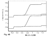
図4Aは、図2Bにおける空乏化した公称非ドープ(直径60nm)GaAsナノワイヤ105の局所的な変換を概略的に示している。図中、電圧がラップゲート電極111、112に印加された場合、(p型)基板104に最近接する第1の領域121はp型導電性に変換され、ナノワイヤのn型端子に最近接する第2の領域122はn型導電性に変換される。これらのラップゲート電極111、112は、その間に共通の電圧源を有する1つの電気回路の一部分であってもよい。これにより、変換された領域間の界面は移動される。ゲートにおいてゼロ電位の場合には、ナノワイヤ105は空乏化され、2つのゲート111、112において+/−3Vの場合には、nドープ及びpドープされた動作が類似する。バイアスが基板とn型端子との間に印加された場合、これは、一例として、ナノLEDとして使用するために、擬似的なpn接合として動作する。本発明の1つの実施形態において、半導体デバイスは、例えば、ナノワイヤの長さに沿って傾斜組成を有する波長調整可能なLEDを得るために、LEDの再結合領域がナノワイヤの長さに沿って移動されることを可能にする少なくとも2つのラップゲート電極を有するLEDとして機能できる。傾斜組成は、ナノワイヤの長さに沿って異なる組成のセグメントを含んでもよい。変化する寸法、即ち、直径は、ナノワイヤの長さに沿い、調整可能なLEDを達成するために単独で又は変化する組成と組み合わせて使用可能である。図4Bは、印加されたバイアスによる挙動を概略的に示し、図4Cは、0Vのバイアス及び1.3Vのバイアスにおける電子及び正孔の空間分布を示している。
FIG. 4A schematically illustrates the local conversion of the depleted nominally undoped (60 nm diameter)
図5A及び図5Bを参照するに、本発明における半導体デバイスの1つの実施形態は、長さに沿って分布される一連の量子井戸115を有する第1のナノワイヤ105を含む。1つ以上のラップゲート電極は、量子井戸の組成により判定された所定の波長を有する光を生成するために量子井戸のいずれかに対して光を生成するように再結合領域の調整を可能にするナノワイヤの長さに沿って異なる位置に配置される。このように、ナノワイヤLEDデバイスにおいて離散的な波長を切り替えることが考えられる。複数のナノワイヤから射出された光の波長は、より幅の広いスペクトルを有するように組み合わされてもよい。図5Aは、第1のラップゲート電極と第2のラップゲート電極との間の位置において異なる組成の2つの量子井戸を有するナノワイヤ105を示している。第1のラップゲート電極111及び第2のラップゲート電極112に印加された電圧を変更することにより、電荷キャリア型を真性からp型又はn型に変更したナノワイヤ105の部分の拡張部分の拡張が変更される。これにより、再結合領域は、量子井戸のいずれかに対して移動される。図5Bは、不動態の真性導電型を有する第1の縦方向領域121に配置された第1のゲート111のみを含む別の実施形態を示している。第2の縦方向領域122において、ナノワイヤはp型である。再結合領域は、第1の領域121と第2の領域122との間の異なる組成の2つの量子井戸間で移動可能である。
With reference to FIGS. 5A and 5B, one embodiment of a semiconductor device in accordance with the present invention includes a
上述したように、ナノワイヤのドーピングは困難である。特に、III−V族窒化物半導体、例えば、GaNのMgドーピングは困難である。ナノワイヤLED等のこの種の材料からなる半導体デバイスの性能は、ラップゲートを使用して再結合領域の正孔の濃度を増加することにより向上される。 As mentioned above, nanowire doping is difficult. In particular, Mg doping of III-V nitride semiconductors such as GaN is difficult. The performance of semiconductor devices made of this type of material, such as nanowire LEDs, is improved by using a wrap gate to increase the concentration of holes in the recombination region.
図6を参照するに、本発明における半導体デバイスの1つの実施形態は、ナノワイヤコア207と、コア207にエピタキシャル配置され、且つ、少なくとも部分的にナノワイヤコア207を取り囲み、径方向のヘテロ構造を提供する少なくとも第1のシェル層208とを含む少なくとも第1のナノワイヤ205を含む。少なくとも第1のラップゲート電極211は、ナノワイヤ205の第1の領域221に配置される。
Referring to FIG. 6, one embodiment of a semiconductor device in accordance with the present invention includes a
本発明の1つの実施形態において、コア及びコアを取り囲む第1のシェル層で規定された1つ以上の量子井戸の双方は導電し、シェル層におけるキャリア濃度は第1のラップゲートにより制御される。 In one embodiment of the present invention, both the core and one or more quantum wells defined by the first shell layer surrounding the core are conducting, and the carrier concentration in the shell layer is controlled by the first wrap gate. .
本実施形態の1つの実現例において、コア及びシェル層は、ラップゲート電極の起動により電子伝導されるように構成される。本実施形態の別の実現例において、ラップゲート電極の起動により、コアはn伝導されるように構成され、シェルはp伝導されるように構成される。本実施形態の更に別の実現例において、電荷キャリア型は調整可能である。 In one implementation of this embodiment, the core and shell layers are configured to conduct electrons upon activation of the wrap gate electrode. In another implementation of this embodiment, upon activation of the wrap gate electrode, the core is configured to be n-conducted and the shell is configured to be p-conducted. In yet another implementation of this embodiment, the charge carrier type is adjustable.
本発明における半導体デバイスの1つの実施形態は、GaAsコア及びAlGaAsシェル層を有するナノワイヤを含む。このコア/シェル構造により、空間間接励起子を形成する機会が可能になり、電子及び正孔は、径方向に分離される。GaAs/AlGaAsコア/シェル構造のコア及びシェル層において再結合する励起子から得られるPLの具体例を図4に示す。 One embodiment of a semiconductor device in the present invention includes a nanowire having a GaAs core and an AlGaAs shell layer. This core / shell structure allows the opportunity to form spatial indirect excitons, and electrons and holes are separated in the radial direction. FIG. 4 shows a specific example of PL obtained from excitons that recombine in the core and shell layers of the GaAs / AlGaAs core / shell structure.
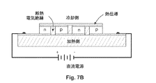
図7A及び図7Bを参照するに、本発明の1つの実施形態において、半導体デバイスは熱電素子である。ラップゲートで制御されるナノワイヤ305により、室温熱電において本発明の熱電素子を使用することが可能となる。一般に、ナノワイヤに基づいた技術は、従来の冷却及び電力変換技術を超えるエネルギー変換効率を有する熱電材料に対する非常に将来性のある技術であると考えられる。しかしながら、当分野における1つの問題は、熱電対を形成するために、同程度に優れた性能特性を有するp型ナノワイヤ及びn型ナノワイヤの双方が必要となることである。一般に、n型デバイスは、典型的なIII−V族材料において、正孔よりも電子に対する方が実質的に高い移動度を有すると考えられる。本実施形態において、ラップゲート誘導キャリア伝導は、規定しない場合には同一のナノワイヤからp型ナノワイヤ305及びn型ナノワイヤ306を規定し、それらの性能が一致するようにこれらのナノワイヤを調整し、それにより、例えば、熱電対又はペルチェ素子等の熱電素子の性能を最適化するために使用される。本実施形態の1つの実現例において、n領域及びp領域のチェッカーボードパターンを有するウエハ全体は、加熱/冷却するための熱電効果を提供するために動作される。
Referring to FIGS. 7A and 7B, in one embodiment of the present invention, the semiconductor device is a thermoelectric element. The
本発明の別の実施形態において、半導体デバイスが熱電素子として機能する場合、半導体デバイスは、上述したように、径方向のヘテロ構造、即ち、n型コア307及びp型シェル層308を含むナノワイヤを含む。少なくとも第1のラップゲート電極311は、ナノワイヤ305の第1の領域321を取り囲むと共に、単一ナノワイヤペルチェ素子を形成する。非常に多数のそのようなナノペルチェ素子のアレイは冷却又は電力生成に使用されるが、単一のそのような素子は非常に効果的なナノスポット冷却器であってもよい。
In another embodiment of the present invention, when the semiconductor device functions as a thermoelectric element, the semiconductor device may include a radial heterostructure, ie, a nanowire including an n-type core 307 and a p-type shell layer 308, as described above. Including. At least the first wrap gate electrode 311 surrounds the first region 321 of the
本発明の1つの実施形態は、スピントロニクスに関する。本実施形態において、ラップゲート誘導キャリア変調は、低濃度ドープされた磁気半導体の強磁性特性を構成及び操作するために使用される。自由キャリア、即ち、自由正孔は、殆どの場合に最大%レベルまでの濃度を有するMn不純物である磁気不純物の間を媒介し、且つ、その間のスピン結合を誘導する。これまで、強磁性挙動を招くキャリア媒介スピン結合は、正孔濃度がMnドーピング濃度と密接に関連付けられるため、制御することが非常に困難であった。本発明において、上述した方法で磁気半導体を含むナノワイヤの周囲に1つ以上のラップゲートを配置することにより、ラップゲート誘導キャリア変調を使用して自由キャリア濃度を別個に調整することができる。 One embodiment of the invention relates to spintronics. In this embodiment, wrap gate induced carrier modulation is used to configure and manipulate the ferromagnetic properties of lightly doped magnetic semiconductors. Free carriers, i.e. free holes, mediate between magnetic impurities, most often Mn impurities with concentrations up to the maximum level, and induce spin coupling therebetween. Heretofore, carrier-mediated spin coupling leading to ferromagnetic behavior has been very difficult to control because the hole concentration is closely related to the Mn doping concentration. In the present invention, the free carrier concentration can be adjusted separately using wrap gate induced carrier modulation by placing one or more wrap gates around a nanowire containing a magnetic semiconductor in the manner described above.
本実施形態の1つの実現例において、本発明における半導体デバイスは、強磁性のオン及びオフを切り替えるために外部ゲートが使用されるMnドープIII−V族ナノワイヤの高密度のアレイを含む。このデバイスは、磁気記憶装置に使用される。例えば、行及び列にナノワイヤを配置することにより、単一ナノワイヤが容易に対処される。ナノワイヤの1次元特性及び2次元アレイ構成により判定された異方性は、従来の記憶媒体と比較して高い温度になるほど性能を向上する。上述した擬似的な接合を作成し、且つ、複数の領域を調整可能なLEDを提供するために、ナノワイヤのゲート制御と同様に、1つのナノワイヤの複数領域の強磁性特性は、ナノワイヤの長さに沿って配置された複数のラップゲートにより制御される。強磁性特性の構成及び操作を行うためのラップゲート誘導キャリア変調の基本的な構造は、図1A及び図2Aに最もよく示されている。ナノワイヤの電荷キャリア濃度は、電荷キャリア型を変更するためでなく、強磁性特性が変更されるように、局所的に制御される。 In one implementation of this embodiment, the semiconductor device in the present invention comprises a dense array of Mn-doped III-V nanowires in which an external gate is used to switch ferromagnetism on and off. This device is used for magnetic storage devices. For example, single nanowires are easily addressed by placing nanowires in rows and columns. The anisotropy determined by the one-dimensional characteristics and the two-dimensional array configuration of the nanowire improves the performance as the temperature becomes higher than that of the conventional storage medium. In order to create a pseudo-junction as described above and to provide a multi-region tunable LED, as well as nanowire gating, the ferromagnetic properties of multiple regions of a single nanowire is the length of the nanowire. Are controlled by a plurality of wrap gates arranged along the line. The basic structure of wrap gate induced carrier modulation for performing and manipulating ferromagnetic properties is best shown in FIGS. 1A and 2A. The charge carrier concentration of the nanowire is controlled locally so as to change the ferromagnetic properties, not to change the charge carrier type.
本発明における半導体デバイスのナノワイヤは、従来技術において使用されていたものより直径が小さくてもよい。従来技術の半導体デバイスのナノワイヤの直径は、典型的には、30nmを超え、30〜50nmの範囲である場合が多い。本発明により、直径が30nm未満、好ましくは、20nm未満であり、更に好ましくは、10〜20nmの範囲であるナノワイヤが使用可能である。これは、実質的に非ドープのナノワイヤの電荷キャリア濃度及び/又は電荷キャリア型の変調が使用されるため可能である。しかしながら、本発明は均一なナノワイヤに限定されず、ナノワイヤの長さに沿って傾斜組成又は変化する組成を有するナノワイヤが使用されてもよい。更に、上述したように、径方向のヘテロ構造が使用されてもよい。 The nanowires of the semiconductor device in the present invention may be smaller in diameter than those used in the prior art. The diameter of nanowires in prior art semiconductor devices is typically greater than 30 nm and often in the range of 30-50 nm. According to the invention, nanowires with a diameter of less than 30 nm, preferably less than 20 nm, more preferably in the range of 10-20 nm can be used. This is possible because a substantially undoped nanowire charge carrier concentration and / or charge carrier type modulation is used. However, the present invention is not limited to uniform nanowires, and nanowires having a gradient composition or a composition that varies along the length of the nanowire may be used. Furthermore, as described above, radial heterostructures may be used.
本発明により、広い範囲にわたってキャリア濃度を操作できるようになり、ナノワイヤに沿った種々のセグメントごとに独立してこれを行える。これは電荷反転を含む。この方法により、理想的な1次元ナノワイヤにおけるフェルミエネルギーが完全に調整される。 The present invention allows the carrier concentration to be manipulated over a wide range, which can be done independently for the various segments along the nanowire. This includes charge reversal. This method completely adjusts the Fermi energy in an ideal one-dimensional nanowire.
超短ゲート長(約50nm)を作成した経験に基づいて、そのようなラップゲートを垂直に積み重ねることができる。これにより、単一量子ドット又は単一電子ターンスタイル設計によるナノワイヤの長さに沿ったナノワイヤの輸送チャネルの制御が可能になる。 Based on experience creating ultra-short gate lengths (about 50 nm), such wrap gates can be stacked vertically. This allows control of the nanowire transport channel along the length of the nanowire with a single quantum dot or single electron turnstyle design.
単一ナノワイヤに関して本発明を説明したが、大量(数個〜数百万個)のナノワイヤが同一の方法で統括的にゲート制御されてもよいことが理解される。 Although the present invention has been described with respect to a single nanowire, it is understood that large numbers (several to millions) of nanowires may be centrally gated in the same manner.
現時点で最も実用的で好適な実施形態であると考えられるものに関連して本発明を説明したが、本発明は、開示した実施形態に限定されることを意図せず、添付の請求項の範囲内の種々の変形及び同等な構成を範囲に含むことを意図する。 Although the present invention has been described in connection with what are presently considered to be the most practical and preferred embodiments, it is not intended that the invention be limited to the disclosed embodiments, but of the appended claims. Various modifications and equivalent configurations within the scope are intended to be included in the scope.
Claims (23)
前記第1のナノワイヤ(105)は、第1の導電型の第1の縦方向領域(121)と、第2の導電型の第2の縦方向領域(122)と、前記ナノワイヤ(150)の前記第1の縦方向領域(121)に配置された少なくとも第1のラップゲート電極とを備え、電圧が前記第1のラップゲート電極(111)に印加された場合に前記第1の縦方向領域(121)と関連付けられた前記ナノワイヤ(105)の少なくとも第1の部分(101)において電荷キャリア濃度を変更することを特徴とする半導体デバイス。 A semiconductor device comprising at least a first semiconductor nanowire (105), comprising:
The first nanowire (105) includes a first conductivity type first longitudinal region (121), a second conductivity type second longitudinal region (122), and the nanowire (150). At least a first wrap gate electrode disposed in the first vertical region (121), and the first vertical region when a voltage is applied to the first wrap gate electrode (111). A semiconductor device characterized in that the charge carrier concentration is changed in at least a first part (101) of the nanowire (105) associated with (121).
電圧が前記第1のラップゲート電極(111)に印加された場合に前記第1のナノワイヤ(105)の前記第1の領域(121)の強磁性特性、又は、電荷キャリア濃度及び/又は電荷キャリア型を変更するステップを含むことを特徴とする方法。 A method of modulating the characteristics of the first nanowire (105) using at least a first wrap gate electrode (111) disposed in a first region (121) of the first nanowire (105). ,
Ferromagnetic properties of the first region (121) of the first nanowire (105) or charge carrier concentration and / or charge carrier when a voltage is applied to the first wrap gate electrode (111) A method comprising the step of changing the mold.
Applications Claiming Priority (3)
| Application Number | Priority Date | Filing Date | Title |
|---|---|---|---|
| SE0800853-4 | 2008-04-15 | ||
| SE0800853 | 2008-04-15 | ||
| PCT/SE2009/050388 WO2009128777A1 (en) | 2008-04-15 | 2009-04-15 | Nanowire wrap gate devices |
Publications (2)
| Publication Number | Publication Date |
|---|---|
| JP2011523200A true JP2011523200A (en) | 2011-08-04 |
| JP2011523200A5 JP2011523200A5 (en) | 2012-06-07 |
Family
ID=41199335
Family Applications (1)
| Application Number | Title | Priority Date | Filing Date |
|---|---|---|---|
| JP2011504964A Pending JP2011523200A (en) | 2008-04-15 | 2009-04-15 | Nanowire wrap gate device |
Country Status (6)
| Country | Link |
|---|---|
| US (1) | US20110089400A1 (en) |
| EP (1) | EP2262723A4 (en) |
| JP (1) | JP2011523200A (en) |
| KR (1) | KR20100137566A (en) |
| CN (1) | CN102007067A (en) |
| WO (1) | WO2009128777A1 (en) |
Cited By (3)
| Publication number | Priority date | Publication date | Assignee | Title |
|---|---|---|---|---|
| WO2015125823A1 (en) * | 2014-02-18 | 2015-08-27 | 国立大学法人九州大学 | Semiconductor single crystal and power generation method using same |
| JP2016027637A (en) * | 2014-06-27 | 2016-02-18 | コミッサリア ア レネルジー アトミーク エ オ ゼネルジ ザルタナテイヴ | Pn junction optoelectronic device for ionizing dopant by electric field effect |
| JP7555128B2 (en) | 2019-05-21 | 2024-09-24 | アルディア | Optoelectronic devices with light emitting diodes |
Families Citing this family (18)
| Publication number | Priority date | Publication date | Assignee | Title |
|---|---|---|---|---|
| JP5364549B2 (en) * | 2009-12-07 | 2013-12-11 | 日置電機株式会社 | Thermopile type infrared detecting element and method for manufacturing the same |
| CN102222753A (en) * | 2010-04-14 | 2011-10-19 | 中芯国际集成电路制造(上海)有限公司 | LED (Light Emitting Diode) chip packaging structure and packaging method thereof |
| JP5688751B2 (en) * | 2010-06-22 | 2015-03-25 | 日本電信電話株式会社 | Semiconductor device |
| US9478699B2 (en) * | 2010-08-26 | 2016-10-25 | The Ohio State University | Nanoscale emitters with polarization grading |
| FR2975532B1 (en) * | 2011-05-18 | 2013-05-10 | Commissariat Energie Atomique | ELECTRICAL CONNECTION IN SERIES OF LIGHT EMITTING NANOWIRES |
| EP2670702A1 (en) * | 2011-02-01 | 2013-12-11 | QuNano AB | Nanowire device for manipulating charged molecules |
| FR2976123B1 (en) | 2011-06-01 | 2013-07-05 | Commissariat Energie Atomique | SEMICONDUCTOR STRUCTURE FOR EMITTING LIGHT AND METHOD FOR PRODUCING SUCH STRUCTURE |
| KR20150036229A (en) | 2012-07-06 | 2015-04-07 | 큐나노 에이비 | Radial nanowire esaki diode devices and methods |
| FR2999806A1 (en) | 2012-12-19 | 2014-06-20 | Commissariat Energie Atomique | METHOD FOR MANUFACTURING A STRUCTURE, IN PARTICULAR OF A MIS TYPE, PARTICULARLY FOR LIGHT EMITTING DIODE |
| WO2014138904A1 (en) * | 2013-03-14 | 2014-09-18 | The Royal Institution For The Advancement Of Learning/Mcgill University | Methods and devices for solid state nanowire devices |
| GB2518679A (en) | 2013-09-30 | 2015-04-01 | Ibm | Reconfigurable tunnel field-effect transistors |
| US9257527B2 (en) | 2014-02-14 | 2016-02-09 | International Business Machines Corporation | Nanowire transistor structures with merged source/drain regions using auxiliary pillars |
| KR102373620B1 (en) | 2015-09-30 | 2022-03-11 | 삼성전자주식회사 | Semiconductor device |
| US9627478B1 (en) * | 2015-12-10 | 2017-04-18 | International Business Machines Corporation | Integrated vertical nanowire memory |
| TWI604605B (en) * | 2016-12-15 | 2017-11-01 | 國立交通大學 | Semiconductor device and method of manufacturing the same |
| US9847391B1 (en) * | 2017-04-05 | 2017-12-19 | Globalfoundries Inc. | Stacked nanosheet field-effect transistor with diode isolation |
| US10665669B1 (en) | 2019-02-26 | 2020-05-26 | Globalfoundries Inc. | Insulative structure with diffusion break integral with isolation layer and methods to form same |
| GB2601373B (en) * | 2020-11-30 | 2023-10-11 | Plessey Semiconductors Ltd | Voltage-controllable monolithic native RGB arrays |
Citations (4)
| Publication number | Priority date | Publication date | Assignee | Title |
|---|---|---|---|---|
| JPH0425175A (en) * | 1990-05-21 | 1992-01-28 | Canon Inc | Diode |
| JP2007501525A (en) * | 2003-08-04 | 2007-01-25 | ナノシス・インコーポレイテッド | Nanowire composites and systems and methods for making electronic substrates derived therefrom |
| US20070052012A1 (en) * | 2005-08-24 | 2007-03-08 | Micron Technology, Inc. | Vertical tunneling nano-wire transistor |
| WO2008034850A2 (en) * | 2006-09-19 | 2008-03-27 | Qunano Ab | Assembly of nanoscaled field effect transistors |
Family Cites Families (12)
| Publication number | Priority date | Publication date | Assignee | Title |
|---|---|---|---|---|
| EP1159761B1 (en) * | 1999-02-22 | 2010-04-21 | Joseph E. Clawson, Jr. | Electronic nanostructure device |
| US7385262B2 (en) * | 2001-11-27 | 2008-06-10 | The Board Of Trustees Of The Leland Stanford Junior University | Band-structure modulation of nano-structures in an electric field |
| US7335908B2 (en) * | 2002-07-08 | 2008-02-26 | Qunano Ab | Nanostructures and methods for manufacturing the same |
| ATE360873T1 (en) * | 2002-07-25 | 2007-05-15 | California Inst Of Techn | SUBLITHOGRAPHIC NANODOGE STORAGE ARCHITECTURE |
| US7051945B2 (en) * | 2002-09-30 | 2006-05-30 | Nanosys, Inc | Applications of nano-enabled large area macroelectronic substrates incorporating nanowires and nanowire composites |
| DE102004005363A1 (en) * | 2004-02-03 | 2005-09-08 | Forschungszentrum Jülich GmbH | Semiconductor structure |
| AU2006258261A1 (en) * | 2005-06-16 | 2006-12-21 | Qunano Ab | Semiconductor nanowire transistor |
| JP2007184566A (en) * | 2005-12-06 | 2007-07-19 | Canon Inc | Semiconductor element using semiconductor nanowire, and display device and imaging device employing same |
| EP1804286A1 (en) * | 2005-12-27 | 2007-07-04 | Interuniversitair Microelektronica Centrum | Elongate nanostructure semiconductor device |
| DE102006009721B4 (en) * | 2006-03-02 | 2011-08-18 | Qimonda AG, 81739 | Nanowire (nanowire) memory cell and method of making same |
| EP1901354B1 (en) * | 2006-09-15 | 2016-08-24 | Imec | A tunnel field-effect transistor with gated tunnel barrier |
| US8120115B2 (en) * | 2007-03-12 | 2012-02-21 | Imec | Tunnel field-effect transistor with gated tunnel barrier |
-
2009
- 2009-04-15 EP EP09733382.7A patent/EP2262723A4/en not_active Withdrawn
- 2009-04-15 JP JP2011504964A patent/JP2011523200A/en active Pending
- 2009-04-15 WO PCT/SE2009/050388 patent/WO2009128777A1/en active Application Filing
- 2009-04-15 US US12/937,871 patent/US20110089400A1/en not_active Abandoned
- 2009-04-15 CN CN2009801142030A patent/CN102007067A/en active Pending
- 2009-04-15 KR KR1020107025532A patent/KR20100137566A/en not_active Application Discontinuation
Patent Citations (4)
| Publication number | Priority date | Publication date | Assignee | Title |
|---|---|---|---|---|
| JPH0425175A (en) * | 1990-05-21 | 1992-01-28 | Canon Inc | Diode |
| JP2007501525A (en) * | 2003-08-04 | 2007-01-25 | ナノシス・インコーポレイテッド | Nanowire composites and systems and methods for making electronic substrates derived therefrom |
| US20070052012A1 (en) * | 2005-08-24 | 2007-03-08 | Micron Technology, Inc. | Vertical tunneling nano-wire transistor |
| WO2008034850A2 (en) * | 2006-09-19 | 2008-03-27 | Qunano Ab | Assembly of nanoscaled field effect transistors |
Cited By (3)
| Publication number | Priority date | Publication date | Assignee | Title |
|---|---|---|---|---|
| WO2015125823A1 (en) * | 2014-02-18 | 2015-08-27 | 国立大学法人九州大学 | Semiconductor single crystal and power generation method using same |
| JP2016027637A (en) * | 2014-06-27 | 2016-02-18 | コミッサリア ア レネルジー アトミーク エ オ ゼネルジ ザルタナテイヴ | Pn junction optoelectronic device for ionizing dopant by electric field effect |
| JP7555128B2 (en) | 2019-05-21 | 2024-09-24 | アルディア | Optoelectronic devices with light emitting diodes |
Also Published As
| Publication number | Publication date |
|---|---|
| EP2262723A4 (en) | 2014-05-14 |
| CN102007067A (en) | 2011-04-06 |
| US20110089400A1 (en) | 2011-04-21 |
| KR20100137566A (en) | 2010-12-30 |
| EP2262723A1 (en) | 2010-12-22 |
| WO2009128777A1 (en) | 2009-10-22 |
Similar Documents
| Publication | Publication Date | Title |
|---|---|---|
| JP2011523200A (en) | Nanowire wrap gate device | |
| US9096429B2 (en) | Nanoelectronic structure and method of producing such | |
| JP6290199B2 (en) | Radial nanowire Esaki diode device and method | |
| US8129763B2 (en) | Metal-oxide-semiconductor device including a multiple-layer energy filter | |
| KR101729597B1 (en) | Tunnel field-effect transistor, method for manufacturing same, and switch element | |
| WO2008079077A2 (en) | Nanoelectronic structure and method of producing such | |
| US20130264544A1 (en) | Nanowire field-effect device with multiple gates | |
| TW201712870A (en) | Tunnel field effect transistor | |
| KR100491051B1 (en) | Optoelectronic device using dual structure nano dots and method for manufacturing the same | |
| US11469104B2 (en) | Nanowire bending for planar device process on (001) Si substrates | |
| TWM274647U (en) | Tunable radiation emitting semiconductor device | |
| JPWO2004112148A1 (en) | Semiconductor device and manufacturing method thereof | |
| US20140145647A1 (en) | Optical Tilted Charge Devices And Techniques | |
| JP2008085090A (en) | Semiconductor laser device and its manufacturing method | |
| KR100462468B1 (en) | Single nano wire and nano devices using thereof | |
| JP5335194B2 (en) | Semiconductor structure | |
| KR20180021586A (en) | Vertical tunneling field-effect transistor and method of fabricating the same | |
| Gutsche et al. | III/V Nanowires for Electronic and Optoelectronic Applications |
Legal Events
| Date | Code | Title | Description |
|---|---|---|---|
| A521 | Request for written amendment filed |
Free format text: JAPANESE INTERMEDIATE CODE: A523 Effective date: 20120410 |
|
| A621 | Written request for application examination |
Free format text: JAPANESE INTERMEDIATE CODE: A621 Effective date: 20120410 |
|
| A131 | Notification of reasons for refusal |
Free format text: JAPANESE INTERMEDIATE CODE: A131 Effective date: 20131206 |
|
| A02 | Decision of refusal |
Free format text: JAPANESE INTERMEDIATE CODE: A02 Effective date: 20140613 |