JP2011523196A - System and method for surface mount electrical connection - Google Patents
System and method for surface mount electrical connection Download PDFInfo
- Publication number
- JP2011523196A JP2011523196A JP2011513602A JP2011513602A JP2011523196A JP 2011523196 A JP2011523196 A JP 2011523196A JP 2011513602 A JP2011513602 A JP 2011513602A JP 2011513602 A JP2011513602 A JP 2011513602A JP 2011523196 A JP2011523196 A JP 2011523196A
- Authority
- JP
- Japan
- Prior art keywords
- connector
- shield
- header
- plate
- ground
- Prior art date
- Legal status (The legal status is an assumption and is not a legal conclusion. Google has not performed a legal analysis and makes no representation as to the accuracy of the status listed.)
- Ceased
Links
Images


Classifications
-
- H—ELECTRICITY
- H01—ELECTRIC ELEMENTS
- H01R—ELECTRICALLY-CONDUCTIVE CONNECTIONS; STRUCTURAL ASSOCIATIONS OF A PLURALITY OF MUTUALLY-INSULATED ELECTRICAL CONNECTING ELEMENTS; COUPLING DEVICES; CURRENT COLLECTORS
- H01R12/00—Structural associations of a plurality of mutually-insulated electrical connecting elements, specially adapted for printed circuits, e.g. printed circuit boards [PCB], flat or ribbon cables, or like generally planar structures, e.g. terminal strips, terminal blocks; Coupling devices specially adapted for printed circuits, flat or ribbon cables, or like generally planar structures; Terminals specially adapted for contact with, or insertion into, printed circuits, flat or ribbon cables, or like generally planar structures
- H01R12/70—Coupling devices
- H01R12/71—Coupling devices for rigid printing circuits or like structures
-
- H—ELECTRICITY
- H01—ELECTRIC ELEMENTS
- H01R—ELECTRICALLY-CONDUCTIVE CONNECTIONS; STRUCTURAL ASSOCIATIONS OF A PLURALITY OF MUTUALLY-INSULATED ELECTRICAL CONNECTING ELEMENTS; COUPLING DEVICES; CURRENT COLLECTORS
- H01R13/00—Details of coupling devices of the kinds covered by groups H01R12/70 or H01R24/00 - H01R33/00
- H01R13/648—Protective earth or shield arrangements on coupling devices, e.g. anti-static shielding
- H01R13/658—High frequency shielding arrangements, e.g. against EMI [Electro-Magnetic Interference] or EMP [Electro-Magnetic Pulse]
- H01R13/6581—Shield structure
- H01R13/6585—Shielding material individually surrounding or interposed between mutually spaced contacts
- H01R13/6588—Shielding material individually surrounding or interposed between mutually spaced contacts with through openings for individual contacts
-
- H—ELECTRICITY
- H01—ELECTRIC ELEMENTS
- H01R—ELECTRICALLY-CONDUCTIVE CONNECTIONS; STRUCTURAL ASSOCIATIONS OF A PLURALITY OF MUTUALLY-INSULATED ELECTRICAL CONNECTING ELEMENTS; COUPLING DEVICES; CURRENT COLLECTORS
- H01R13/00—Details of coupling devices of the kinds covered by groups H01R12/70 or H01R24/00 - H01R33/00
- H01R13/648—Protective earth or shield arrangements on coupling devices, e.g. anti-static shielding
- H01R13/658—High frequency shielding arrangements, e.g. against EMI [Electro-Magnetic Interference] or EMP [Electro-Magnetic Pulse]
- H01R13/6591—Specific features or arrangements of connection of shield to conductive members
- H01R13/65912—Specific features or arrangements of connection of shield to conductive members for shielded multiconductor cable
- H01R13/65918—Specific features or arrangements of connection of shield to conductive members for shielded multiconductor cable wherein each conductor is individually surrounded by shield
-
- H—ELECTRICITY
- H01—ELECTRIC ELEMENTS
- H01R—ELECTRICALLY-CONDUCTIVE CONNECTIONS; STRUCTURAL ASSOCIATIONS OF A PLURALITY OF MUTUALLY-INSULATED ELECTRICAL CONNECTING ELEMENTS; COUPLING DEVICES; CURRENT COLLECTORS
- H01R12/00—Structural associations of a plurality of mutually-insulated electrical connecting elements, specially adapted for printed circuits, e.g. printed circuit boards [PCB], flat or ribbon cables, or like generally planar structures, e.g. terminal strips, terminal blocks; Coupling devices specially adapted for printed circuits, flat or ribbon cables, or like generally planar structures; Terminals specially adapted for contact with, or insertion into, printed circuits, flat or ribbon cables, or like generally planar structures
- H01R12/70—Coupling devices
- H01R12/71—Coupling devices for rigid printing circuits or like structures
- H01R12/72—Coupling devices for rigid printing circuits or like structures coupling with the edge of the rigid printed circuits or like structures
- H01R12/722—Coupling devices for rigid printing circuits or like structures coupling with the edge of the rigid printed circuits or like structures coupling devices mounted on the edge of the printed circuits
- H01R12/725—Coupling devices for rigid printing circuits or like structures coupling with the edge of the rigid printed circuits or like structures coupling devices mounted on the edge of the printed circuits containing contact members presenting a contact carrying strip, e.g. edge-like strip
-
- H—ELECTRICITY
- H01—ELECTRIC ELEMENTS
- H01R—ELECTRICALLY-CONDUCTIVE CONNECTIONS; STRUCTURAL ASSOCIATIONS OF A PLURALITY OF MUTUALLY-INSULATED ELECTRICAL CONNECTING ELEMENTS; COUPLING DEVICES; CURRENT COLLECTORS
- H01R12/00—Structural associations of a plurality of mutually-insulated electrical connecting elements, specially adapted for printed circuits, e.g. printed circuit boards [PCB], flat or ribbon cables, or like generally planar structures, e.g. terminal strips, terminal blocks; Coupling devices specially adapted for printed circuits, flat or ribbon cables, or like generally planar structures; Terminals specially adapted for contact with, or insertion into, printed circuits, flat or ribbon cables, or like generally planar structures
- H01R12/70—Coupling devices
- H01R12/77—Coupling devices for flexible printed circuits, flat or ribbon cables or like structures
- H01R12/79—Coupling devices for flexible printed circuits, flat or ribbon cables or like structures connecting to rigid printed circuits or like structures
Abstract
電気コネクタシステムが、キャリアアセンブリとヘッダーとを有する。キャリアアセンブリは、複数のシールドコネクタと、シールドコネクタの各々へと成端された同軸ケーブルとを有する。ヘッダーは、回路基板への取り付けのために構成された接地タブを各々が有する対向する接地プレートと、その対向するプレートの間にストリップ線路構成で配設された複数のピンとを備える。キャリアアセンブリの同軸ケーブルは、ヘッダー内のピンのストリップ線路構成を通じて、回路基板と電気的に通信する。
【選択図】図1An electrical connector system has a carrier assembly and a header. The carrier assembly has a plurality of shielded connectors and a coaxial cable terminated to each of the shielded connectors. The header includes opposing ground plates, each having a ground tab configured for attachment to a circuit board, and a plurality of pins disposed in a stripline configuration between the opposing plates. The coaxial cable of the carrier assembly is in electrical communication with the circuit board through a stripline configuration of pins in the header.
[Selection] Figure 1
Description
回路基板上の集積回路をケーブル又は電子デバイスに接続することが当該技術分野において知られている。信号は、回路基板に/回路基板から進むときにコネクタの導体を通じて伝播する。信号線密度が比較的低い場合、電気相互接続は困難なく形成される。加えて、低速な信号速度及び/又は低速なデータ速度の用途にコネクタを設計する場合、信号品位の懸念ははるかに小さなものとなる。 It is known in the art to connect an integrated circuit on a circuit board to a cable or electronic device. The signal propagates through the conductors of the connector as it travels to / from the circuit board. If the signal line density is relatively low, the electrical interconnection is formed without difficulty. In addition, when designing connectors for low signal rate and / or low data rate applications, signal quality concerns are much less.
しかしながら、機器製造業者及び消費者は、より高度な信号線密度及びより高速なデータ速度を絶えず望んでいる。 However, device manufacturers and consumers constantly desire higher signal line densities and higher data rates.
既存の高速相互接続ソリューションは通常、複雑であり、緻密に作り上げられた構成部品設計を用いるものであるが、それらの構成部品設計は、わずかな製造上のばらつきにも左右され、したがって製造が不経済でかつ困難となる。 Existing high-speed interconnect solutions are usually complex and use elaborate component designs, but these component designs are also subject to minor manufacturing variations and are therefore difficult to manufacture. It becomes economical and difficult.
発展するエンドユーザーの要求を満たすのに適した方式で、費用性能比を改善され、回路交換速度を高められ、制御された電気特性で信号線密度を向上され、信号品位を改善/制御された、回路基板、ケーブル、又は電子デバイスの間の電気コネクタ及び接続を提供することが望ましい。 Suitable for meeting the needs of evolving end users, improved cost performance ratio, increased circuit replacement speed, improved signal line density with controlled electrical characteristics, improved / controlled signal quality It would be desirable to provide electrical connectors and connections between circuit boards, cables, or electronic devices.
一態様では、キャリアアセンブリとヘッダーとを有する電気コネクタシステムが提供される。キャリアアセンブリは、複数のシールドコネクタと、シールドコネクタの各々へと成端された同軸ケーブルとを有する。ヘッダーは、回路基板に取り付けられるように構成されたはんだ付け用タブを各々が有する対向する接地プレートと、その対向するプレートの間に配設された複数のピンとを有する。キャリアアセンブリがヘッダーに接続されると、キャリアアセンブリの同軸ケーブルは、ヘッダー内のストリップ線路構成を通じて回路基板と電気的に通信する。 In one aspect, an electrical connector system having a carrier assembly and a header is provided. The carrier assembly has a plurality of shielded connectors and a coaxial cable terminated to each of the shielded connectors. The header has opposing ground plates, each having a soldering tab configured to be attached to the circuit board, and a plurality of pins disposed between the opposing plates. When the carrier assembly is connected to the header, the coaxial cable of the carrier assembly is in electrical communication with the circuit board through a stripline configuration in the header.
添付の図面は、実施形態の更なる理解を得るために含められたものであり、本明細書の一部に組み込まれると共に本明細書の一部をなすものである。図面は、実施形態を例示するものであり、この説明と共に実施形態の原理を説明するためのものである。他の実施形態及び実施形態の意図される利点の多くが、以下の詳細な説明を参照して更に理解されると、容易に明らかとなろう。図面の要素は、必ずしも互いに一定の縮尺ではない。同様の参照符号は、対応する類似した部品を示している。
以下の詳細な説明において、添付の図面を参照するが、それらの図面は本願の一部をなすものであり、本発明が実施され得る特定の実施形態を実例として示すものである。この点に関して、「上部」、「下部」、「前部」、「後部」「リーディング」、「トレーリング」などのような方向に関する用語が、記載されている図の方向に関して使われる。各実施形態の構成要素は多数の様々な方向で配置され得るため、方向に関する用語は、説明の目的で用いられており、限定するものではない。他の実施形態が利用されてもよく、また、構造的又は論理的な変更が、本発明の範囲から逸脱することなくなされ得ることを理解されたい。したがって、以下の詳細な説明は、限定的な意味で解釈されるものではなく、本発明の範囲は、添付の特許請求の範囲によって定義される。 In the following detailed description, reference is made to the accompanying drawings, which form a part hereof, and which illustrate by way of illustration specific embodiments in which the invention may be practiced. In this regard, directional terms such as “top”, “bottom”, “front”, “rear”, “leading”, “trailing”, etc. are used with respect to the direction of the described figure. Since the components of each embodiment may be arranged in a number of different directions, the terminology related to directions is used for purposes of explanation and is not limiting. It should be understood that other embodiments may be utilized and structural or logical changes may be made without departing from the scope of the present invention. The following detailed description is, therefore, not to be taken in a limiting sense, and the scope of the present invention is defined by the appended claims.
特に明記しない限り、本明細書で説明する各種の例示的な実施形態の特徴が互いに組み合わされてもよいことが理解されよう。 It will be understood that the features of the various exemplary embodiments described herein may be combined with each other, unless expressly stated otherwise.
本明細書において、「を備える(comprising a, comprising an)」という語句は、1つ以上を含む集合を意味する。 In this specification, the phrase “comprising a, comprising an” means a set including one or more.
本明細書において、ストリップ線路は、空気によって、あるいは誘電体などの絶縁体によって、対向する接地プレートの間に隔置された導電要素を意味する。あるストリップ線路構成は、誘電体によって2枚の対向する接地プレートからある距離を置いて保持された1つ以上の導電要素(例えば、1本以上のピン)である。 As used herein, stripline refers to conductive elements spaced between opposing ground plates by air or by an insulator such as a dielectric. One stripline configuration is one or more conductive elements (eg, one or more pins) held by a dielectric at a distance from two opposing ground plates.
各実施形態は、インピーダンス制御された同軸のケーブル対ストリップ線路の相互接続を提供するものであり、その相互接続は、キャリアアセンブリと嵌合するヘッダーを有する。キャリアアセンブリの同軸ケーブルの中心導体は、ストリップ線路ヘッダーの信号ピンと結合する。キャリアアセンブリの同軸ケーブルシールドは、ストリップ線路ヘッダーの接地プレートと結合する。一実施形態においては、双方の接地プレートが回路基板に装着される。別の実施形態においては、ヘッダーの一方の接地プレートはプリント回路基板の一部分として一体的に形成され、ケーブルシールドは、コネクタシールド本体の接地接点を介してそれに結合する。 Each embodiment provides an impedance controlled coaxial cable-to-stripline interconnection, the interconnection having a header that mates with the carrier assembly. The center conductor of the carrier assembly coaxial cable couples to the signal pin of the stripline header. The coaxial cable shield of the carrier assembly is coupled to the ground plate of the stripline header. In one embodiment, both ground plates are attached to the circuit board. In another embodiment, one ground plate of the header is integrally formed as part of the printed circuit board, and the cable shield is coupled to it through the ground contact of the connector shield body.
ヘッダーの各実施形態により、電磁気干渉(EMI)に対する遮蔽が得られる。キャリアの各実施形態により、キャリアアセンブリ内に配設されたシールド付きのインピーダンス制御されたコネクタを使用することで信号品位性能が改善される。 Each embodiment of the header provides shielding against electromagnetic interference (EMI). Each embodiment of the carrier improves signal quality performance by using a shielded impedance controlled connector disposed within the carrier assembly.
ヘッダーの一実施形態により、通常の直角型の表面実装ヘッダーの全体にわたって帯域幅を改善するように構成されたストリップ線路構成が得られる。ヘッダーの一実施形態により、プリント回路基板の接地パッドに施される高価な金メッキの使用が排除される。本明細書で説明するヘッダーは、通常のヘッダーよりも約50パーセント超小型の全高を有するパッケージにて提供される。ヘッダー/キャリアアセンブリの他の実施形態により、インピーダンス制御を改善した上で通常の相互接続よりも約30パーセント超、帯域幅が改善される。 One embodiment of the header provides a stripline configuration that is configured to improve bandwidth throughout a normal right angle surface mount header. One embodiment of the header eliminates the use of expensive gold plating applied to the ground pad of the printed circuit board. The header described herein is provided in a package having an overall height that is approximately 50 percent smaller than a regular header. Other embodiments of the header / carrier assembly improve bandwidth by over about 30 percent over regular interconnects with improved impedance control.
一実施形態において、このヘッダーにより、直角型の高速ハードメトリックコネクタに嵌合する費用を伴うことなく、プリント回路基板への直角型の表面実装相互接続が得られる。ヘッダーの各実施形態は、一体に結合してシェルを形成する構造化プレートを提供し、そのシェルは、従来のヘッダーで用いられていた、高コストで精密に穿孔及びメッキされる貫通孔の支持インターフェースを排除するものである。メッキされる貫通孔を排除することにより、基板トレース配線領域が増加する。メッキされる貫通孔を削減又は排除することにより、穴に関連する静電容量が減少するが、この静電容量は通常、従来の相互接続においてインピーダンス制御の変動を引き起こしている。 In one embodiment, the header provides a right angle surface mount interconnect to the printed circuit board without the expense of mating with a right angle high speed hard metric connector. Each embodiment of the header provides a structured plate that is joined together to form a shell, which supports the high-cost, precisely drilled and plated through-holes used in conventional headers. It eliminates the interface. By eliminating the plated through holes, the substrate trace wiring area is increased. By reducing or eliminating plated through holes, the capacitance associated with the holes is reduced, but this capacitance typically causes variations in impedance control in conventional interconnects.
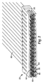
図1は、一実施形態による電気コネクタシステム20の部分分解斜視図である。電気コネクタシステム20は、インピーダンス制御されたストリップ線路ヘッダー24と嵌合するように構成されたキャリアアセンブリ22を有している。キャリアアセンブリ22は、ハウジング28内に保持された複数のシールドコネクタ26を有しており、シールドコネクタ26の各々は同軸ケーブル30へと成端している。具体的に言えば、各シールドコネクタ26は、ケーブル30の中心導体31に接続された接点32と、ケーブル30のシールド33に接続されたシールド本体34とを有しており、シールド本体34は絶縁体35の周りに配設され、絶縁体35は接点32の周りに配設される。誘電体37が、中心導体31をシールド33から分離している。
FIG. 1 is a partially exploded perspective view of an
ケーブル30は、コンタクト32及びシールド本体34へと成端するように構成された同軸ケーブルである。好適なシールドコネクタが、2007年1月25日出願の米国特許公開第20070197095号において例えば段落[0041]〜[0044]及び図6〜図9Fに記載されており、その記載内容は本願に組み込まれる。
The
シールド本体34は、ラッチ36と接地ビーム38とを有している。シールド本体34は全体として、ケーブル30の成端部に環状の外殻を形成している。シールド本体34は、円筒状の外殻、正方形の横断面形状を有する外殻、又は、長方形の横断面形状を有する外殻など、任意の好適な形状を有している。一実施形態において、ラッチ36は、接地ビーム38が形成されている表面から分離された表面に形成される。ラッチ36は、シールド本体34をハウジング28内に固定するように構成されている。1つ以上の接地ビーム38が、シールド本体34の表面から突出している。一実施形態において、シールド本体34は、対向する2つの接地ビーム38を有し、例えば、図1において方向付けられているように、一方はシールド本体34の上部表面から突出し、もう一方はシールド本体34の下部表面から突出する。
The
ヘッダー24は、第2のプレート42と結合してシェル44を画定する第1のプレート40を有しており、シェル44は、1組みの信号ピン(図4を参照)を、接点32と嵌合させるための整列した構成に維持する。第1のプレート40は、シールド本体34の第1の側で接地ビーム38と結合するように構成されており、プリント回路基板に取り付けられるように構成された複数のはんだ付け用タブ46を有している。第2のプレート42は、反対側のシールド本体34の第2の側に設けられた接地ビーム38と結合するように構成されており、プリント回路基板に取り付けられるように構成された複数のはんだ付け用タブ48を有している。一実施形態において、はんだ付け用タブ46は、はんだ付け用タブ48と交互に並ぶ位置にあり、そのため、シェル44の後方端は実質的に、互いに組み合うはんだ付け用タブ46、48で囲まれ、それらのはんだ付け用タブ46、48を有する。
The
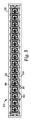
図2はキャリアアセンブリ22の斜視図であり、図3はキャリアアセンブリ22の正面図である。一実施形態において、ハウジング28が、単列のシールドコネクタ26の周りに配設され、それらシールドコネクタ26を支持する。一実施形態において、16本のシールドコネクタ26が単列で配設されるが、他の本数のシールドコネクタ26がハウジング28によって保持されることもまた適格となる。シールドコネクタ26を正確に方向付ける、あるいは編成することが望ましい。一実施形態において、分離プレート60が、ハウジング28の対向する主要表面62、64の間に延びて、隣接するシールドコネクタ26を分離する。一実施形態において、分離プレート60はタブ66を有し、タブ66は、シールドコネクタ26と係合してシールドコネクタ26を実質的に一定の位置合わせされた姿勢に方向付けるように構成される。
FIG. 2 is a perspective view of the
一実施形態において、ハウジング28は、プラスチックなどの電気絶縁材料から製作され、分離プレート66は、金属などの薄い硬質材料から製作される。ハウジング28は、機械加工及び/又はミリング加工されたハウジングと比べて費用性能比が改善されるように、例えば成型によって製作される。分離プレート66も、費用性能比が改善されるように製作され、ハウジング28と互換性がある。分離プレート66は、薄くかつ小型であると同時に、非常に硬質であり、ハウジング28内でシールドコネクタ26を正確に方向付けるものである。
In one embodiment, the
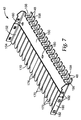
図4は、ヘッダー24の分解斜視図である。一実施形態において、ヘッダー24は複数の信号ピン70を有し、それらの信号ピン70は、第1のプレート40と第2のプレート42との間で誘電支持体72によって保持される。一実施形態において、ピン70は信号ピンを含み、各ピンは接触部分80と成端部分86とを有し、成端部分86は、接触部分80から延びる尾部82と尾部82から延びるはんだ付け用尾部84とを有する。接触部分80は、接点32(図1)との電気接触をなすように構成されている。一実施形態において、信号ピン70は、直角型の信号ピンを形成し、はんだ付け用尾部84は、プリント回路基板に取り付けられると、尾部82がプリント回路基板に対して実質的に垂直となり、接触部分80がプリント回路基板に対して実質的に平行となるように構成されている。誘電支持体72は、正確に位置合わせされたシールドコネクタ26(図1)と結合するために、正確に位置合わせされた構成で信号ピン70を保持するように構成されている。誘電支持体72は、組み立てられると、隣接するピン70同士の間の誘電距離が、ピン70のうちの1本と、対向する第1および第2のプレート40、42との間に延びる誘電厚さの約2倍となることによって、ストリップ線路ヘッダー24の各ピン70に対するクロストークが最小化されるように構成されている。
FIG. 4 is an exploded perspective view of the
図5は、誘電支持体72の斜視図である。一実施形態において、誘電支持体72は、アーム92同士の間に延びるブリッジ90を有している。ブリッジ90は複数のスロット94を画定しており、各スロット94は、1本のピンを位置合わせし保持するように構成されている(図4)。一実施形態において、ブリッジ90は、上部表面98上の位置合わせ用ポスト96と、その反対側の下部表面上の位置合わせ用ポスト(図示せず)とを有している。位置合わせ用ポスト96は、第1のプレート40(図4)と結合して誘電支持体72をシェル44に対して定位置に固定するように構成されている。このようにして、誘電支持体70は、シェル44に対する移動を最小限としており、また誘電体72によって保持されるピン70も同様に、第1のプレート40及び第2のプレート42に対する移動を最小限としている。
FIG. 5 is a perspective view of the
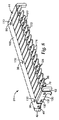
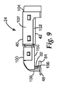
図6は、第1のプレート40の斜視図である。第1のプレート40は、基部100と、基部100から延び前方端104にて成端する前方端部分102と、基部100から延び後方端108にて成端する後方端部分106とを有している。はんだ付け用タブ46が後方端部分106から後方端108へと延びている。一実施形態において、基部100は、位置合わせ用ポスト96(図5)を受容するように構成された位置合わせ用窓110を有する。位置合わせ用ポスト96と位置合わせ用窓110は、協働して誘電支持体72を定位置に固定又は保持する。
FIG. 6 is a perspective view of the
一実施形態において、前方端部分102は複数のスロット120を有し、それらのスロット120は、組み合わさって、基部100から延びる複数のフィンガー122を画定する。一実施形態において、スロット120は、前方端104から基部100へ延びており、各フィンガー122の前方端104の一部分124は先細となっている。換言すれば、先細部分124が各フィンガー122の前方端104から幾分かスロット120の中へ延びている。
In one embodiment, the
第1のプレート40は、第2のプレート42とスナップ嵌めされて、誘電支持体72及び誘電支持体72によって保持されたピン70を囲んでストリップ線路構成のヘッダー24を形成するように構成されている。一実施形態において、第1のプレート140の対向する各側部130は開口部132を有しており、開口部132は、第1のプレート40を第2のプレート42とスナップ嵌めできるように構成されている。
The
図7は、第2のプレート42の斜視図である。第2のプレート42は、基部150と、基部150から延び前方端154にて成端する前方端部分152と、後方端158にて成端する後方端部分156とを有している。一実施形態において、第2のプレート42の基部150は、位置合わせ用ポスト96(図5)を受容するように構成された位置合わせ用窓160を画定する。位置合わせ用窓160と位置合わせ用ポスト96は、シェル44の内部にて実質的に一定の方向に誘電支持体72を協働して保持するように構成されている。
FIG. 7 is a perspective view of the
一実施形態において、前方端部分152は、複数のスロット170及び複数のフィンガー172を画定し、各フィンガー172は隣接するスロット170の間に設けられる。一実施形態において、先細部174が各フィンガー172ごとに設けられており、先細部174は前方端154から幾分かスロット170の中へ延びている。
In one embodiment, the
第2のプレート42の対向する側部が、側部180から外向きに延びる突出部182を画定している。突出部182は、開口部132(図6)と係合するように構成されており、そのため、第1のプレート40が第2のプレート42とスナップ嵌めされ、突出部182が開口部132によって受容されるようになっている。
Opposing sides of the
後方端部分156は基部150に対して実質的に直角であり、はんだ付け用タブ48は後方端部分156に対して実質的に直角である。このようにして、後方端部分156は、基部150に対しておおよそ直角に下降しており、はんだ付け用タブ48は、後方端部分156に対しておおよそ直角に延びている。
The
図8はヘッダー24の斜視図であり、図9はヘッダー24の側面図である。ピン70がフィンガー122、172に対して位置合わせされるように、第1のプレート40が、第2のプレート42に結合されて誘電支持体72を支持している。具体的に言えば、位置合わせ用ポスト96が位置合わせ用窓110内に固定されており、ピン70の接触部分80が、第1のプレート40のフィンガー122と第2のプレート42のフィンガー172との間に、かつそれらと平行に位置合わせされている。更に図4を参照すると、ピン70は、ピン70の接触部分80がシェル44の後方端から突出するように、誘電支持体72内に保持される。このようにして、ヘッダー24は直角型の表面実装ヘッダーを形成し、ピン70は接地プレート40、42の間にストリップ線路構成にて設けられる。特に、ピン70の接触部分80とフィンガー122、172により、ヘッダー24はストリップ線路構成を形成している。
FIG. 8 is a perspective view of the
ピン70の尾部分82は実質的に、接触部分80に対して直角であり、フィンガー122、172に対しても直角である。各ピン70の尾部分82は、2つの側部にて第2のプレート42の後方端部分156によってシールドされており、また1つの側部にて第1のプレート40の後方端部分106によってシールドされている。このようにして、ピン70の尾部分82は、少なくとも3つの側部にて、第2のプレート42の横方向に下降する後方端部分156、及び第1のプレート40の平行でありかつずれた後方端部分106によってシールドされている。
The
はんだ付け用尾部84に対するタブ46、48の方向は反対にされ得る(この図ではタブ46がタブ48の後方にある)ことが理解されよう。つまり、タブ46、48は、図9において右に方向付けられることができ、はんだ付け用尾部84は左に方向付けられることができる。一実施形態において、タブ46、48とはんだ付け用尾部84との相対的方向が、図9に示す順序と反対にされ、ヘッダー24は実質的に同様の電気的性能を備えるが、はんだ付け用尾部84のはんだ接続を視覚的に確認する容易性が改善される。
It will be appreciated that the orientation of the
フィンガー122、172は、シールドコネクタ26(図1)のシールド本体34を位置合わせするように構成されている。ピン70は、キャリアアセンブリ22(図1)がヘッダー24に接続されるときにインピーダンスの不連続生を場合によっては生じ得る、介在する壁又は他の支持体を用いることなく、プレート40、42の間に配置されている。このようにして、ヘッダー24は、高速信号向けの相互接続を形成し、インピーダンス制御されたストリップ線路構成を形成するように構成されている。
The
図1及び図6〜7を更に参照すると、キャリアアセンブリ22がヘッダー24に導入されるとき、フィンガー122の間の個々のスロット120が、分離プレート60のうちの対応する1つと係合して、キャリアアセンブリ22に対してヘッダー24をまず横方向に位置合わせする。キャリアアセンブリ22がヘッダー24の中に更に係合することにより、フィンガー122、172がシールド本体34と係合し、フィンガー122、172がシールド本体34を持ち上げて、各シールドコネクタ26の内部の接点32をピン70の接触部分80と正確に位置合わせする。接続されるとき、キャリアアセンブリ22は、ヘッダー24に被さって挿入され、それにより、各ピン70が、キャリアアセンブリ22の内部の位置合わせされた各接点32と係合する。接地ビーム38はフィンガー122、172と接触して、ピン70を通じて伝播する信号の周りの接地マトリクス(ground matrix)を形成する。
With further reference to FIGS. 1 and 6-7, when the
一実施形態において、フィンガー122、172の先細部分124、174はそれぞれ、ヘッダー24の内部の各信号ピン70に対するシールド本体34の横方向の位置合わせを実現し、かつ/又は確実にするように構成されている。加えて、フィンガー122、172の先細部分124、174は、キャリアアセンブリ22の分離プレート60と位置合わせされるように構成された引込み部(lead-in)を形成して、ヘッダー24がキャリアアセンブリ22と係合するときにヘッダー24を垂直方向に(すなわち非横方向に)位置合わせするようになっている。
In one embodiment, the
図10Aはヘッダー24の底面図である。各ピン70(図4)のはんだ付け用尾部84は、プリント回路基板への取り付けに利用可能である。図6及び7を更に参照すると、はんだ付け用タブ46の後方端106がピン70の尾部82をシールドし、またはんだ付け用タブ48の水平部分の付近でピン70の水平側部をシールドしている。
FIG. 10A is a bottom view of the
図10Bは、3つの側面を電磁気干渉からシールドされたピン70の拡大図である。第1のプレート40に形成されたはんだ付け用タブ46の後方端部分106が、距離Aだけピン70の尾部82からずれている。一実施形態において、距離Aは、ヘッダー24のストリップ線路構成のために、制御されたインピーダンスを信号ピン70にもたらすように構成されている。隣接するはんだ付け用タブ48の後方端部分156が、ピン70の水平側部を電磁気干渉からシールドしている。一実施形態において、各はんだ付け用タブ46、48の後方端部分106、156は、ピン70の信号同士の間のクロストークを相当に低減する方式で、ピン70の周囲の約75パーセントを囲むように結合する。換言すれば、各ピン70は実質的に同軸の構造を有し、その構造は、一部を各はんだ付け用タブ46、48の後方端部分106、156によって形成された接地用導体で周囲の約75%を囲まれている。
FIG. 10B is an enlarged view of the
図11は、ヘッダー24に取り付けられたキャリアアセンブリ22を示すシステム20の横断面図である。対向する接地プレート40、42の前方部分は、それぞれ複数のフィンガー122、172を画定しており、各フィンガー122、172は、キャリアアセンブリ22のハウジング28とシールド本体34のうちの1つとの間に捕捉されるように構成されている。一実施形態において、接地ビーム38は、シールド本体34から離れて湾曲すると共にヘッダー24のフィンガーを支持し、それによって、フィンガー122、172をシールド本体34から外向きに又はシールド本体34から離して、かつハウジング28に対抗して押しつける。ハウジング28の壁は、フィンガー122、172が屈曲するのを防止し、したがって、接地ビーム38が接地プレート40、42と確実に接触するようにしている。
FIG. 11 is a cross-sectional view of
図12は、プリント回路基板200に結合された電気コネクタシステム20の斜視図である。ヘッダー24は、少なくともはんだ付け用タブ46、48にてプリント回路基板200にはんだ付けされている。一実施形態において、ヘッダー24は、はんだ付け用タブ46、48にて、またはんだ付け用翼部210にてプリント回路基板200にはんだ付けされる。はんだ付け用翼部210は、相互接続を形成するときにアセンブリ22を湾曲させる又はアセンブリ22/ヘッダー24に損傷を与える危険性を最小化/低減する方式で、ヘッダー24を基板200に固定する更なる固着機構を提供している。一実施形態において、ケーブル30は同軸ケーブルであり、コネクタ26は、キャリアアセンブリ22内に固定され、ヘッダー24内の信号ピンのストリップ線路構成に結合される。このようにして、電気コネクタシステム20により、ヘッダー24内のストリップ線路構成を通じて同軸ケーブル30をプリント回路基板200に電気接続することが可能となっている。
FIG. 12 is a perspective view of the
図8を更に参照すると、キャリアアセンブリ22がヘッダー24に嵌合されるとき、キャリアアセンブリ22の分離プレート60が、対向するプレート40、42のスロット120の中に挿入されて、シールドコネクタ26内の接点32がヘッダー24内のピン70と横方向に位置合わせされる。更に挿入された後、対向するプレート40、42のフィンガー122がシールドコネクタ26を捕捉して、シールドコネクタ26内の接点32をヘッダー24内のピン70と縦方向に位置合わせする。各フィンガー122の各先細部分124は、分離プレート60に対してフィンガー122を位置決めする(又はフィンガー122の配置を調節する)のを支援するように構成されている。
With further reference to FIG. 8, when the
通常の相互接続アセンブリは、支持構造内に形成された位置合わせ用の壁又はソケットを用いて、ケーブルが回路基板へ相互接続されるようにしている。対照的に、コネクタ26は、プリント回路基板200に取り付けられたヘッダー24と直接連通している。ヘッダー24は、介在する壁又は他のそのようなインピーダンスの不連続性を伴うことなく、挿入の間にコネクタ26を位置合わせする。この直接的な形の相互接続により、インピーダンスを制御した方式で高速な信号伝送に向いた電気コネクタシステム20が構成される。
A typical interconnect assembly uses alignment walls or sockets formed in the support structure to allow the cables to be interconnected to the circuit board. In contrast, the
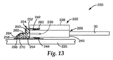
図13は、プリント回路基板225に接続されたキャリアアセンブリ222を有する電気コネクタシステム200の横断面図であり、図14は、プリント回路基板225の加工形体の上面図である。キャリアアセンブリ222は、ヘッダー224に結合された1列のシールドコネクタ226を有している。各シールドコネクタ226は、ヘッダー224によって設けられた接地プレート252と、プリント回路基板225の加工形体として設けられた接地プレート254(又は接地パッド254)との間で接地されている。このようにして、ヘッダー224は、プリント回路基板225と組み合わさって、プリント回路基板225と電気的に通信するケーブル/コネクタに、ストリップ線路構成をもたらしている。ヘッダー224の信号ピン230は、プリント回路基板225と通信しており、キャリアアセンブリ222のコネクタ226を受容するように構成されている。
13 is a cross-sectional view of an
一実施形態において、キャリアアセンブリ222は、ハウジング228内にて単列のシールドコネクタ226を支持するが、他の構成もまた許容される。ハウジング228は、説明を簡単にするため、横断面では示されていない。シールドコネクタ226は、図1にて上述したシールドコネクタ26と実質的に類似しており、ケーブル30は、上述したケーブル30と類似した同軸ケーブルである。
In one embodiment, the
一実施形態において、シールドコネクタ226はシールド本体240を有し、シールド本体240は、ヘッダー224の接地プレート252と接触する第1の接地ワイパー242と、プリント回路基板225の接地プレート254と接触する第2の接地ワイパー244とを有する。接地ワイパー242、244は、弾性があり軟質な接地ビームである。一実施形態において、接地ワイパー244は、接地ワイパー242とは異なるものであり、以下で説明するように、シールド本体240から離れる、より広範な弾力屈曲性を有するように構成される。
In one embodiment, the
ヘッダー224は、1列のピン230を支持する電気絶縁体250を有しており、ピン230は、ストリップ線路構成をヘッダー224に与えるように、接地プレート252及び接地パッド254から分離されている。下部プレート254は、プリント回路基板225と一体となるように製作されるか、あるいはプリント回路基板225の上部表面として設けられる。プレート252は、はんだ256のフィレットによってプリント回路基板225にはんだ付けされており、それにより、場合によってはプレート252及びピン230が基板225から持ち上がる。接地ワイパー244がシールド本体240から完全に離れて延び、かつプリント回路基板225上のプレート254と接触するのを確実にするために、接地ワイパー244は、十分に広範囲に及ぶ弾力的な屈曲性を有するように構成されている。
プレート252は、ピン230の形状に従うように構成されている。プレート252は、前方部分260と、前方部分260から延びる後方部分262と、後方部分262から延びる後方端264と、はんだ付け用タブ266とを有している。ピン230は、絶縁体250内にあるピン230の後方端270が、コネクタ226と結合するピン230の前方端と比べて、プレート254により近い位置にあるように付形されている。この構成を用いると、望ましくかつ電気的に好適な誘電間隔が、ピン230とプリント回路基板225との間に、そしてピン230とプレート252との間に得られる。一実施形態において、絶縁体250は、ピン230に関するこの上述の望ましい間隔を維持するように構造を与えられ、それにより、ほぼ対称的なあるいは釣り合いのとれた静電結合がもたらされ、ヘッダー224はストリップ線路構成を有することになる。具体的に言えば、このストリップ線路構成は、ヘッダー224の接地プレート252と接触する第1の接地ワイパー242、及びプリント回路基板225の接地プレート254と接触する第2の接地ワイパー244によって定められる。
The
プリント回路基板225は、離間された一連の接地区間280と、それと交互に並ぶ一連の信号パッド282とを画定する接地パッド254を有している。各信号パッド282は、隣接する一対の接地区間280の間に配設されている。信号パッド282同士の間隔、及び接地区間280同士の間隔はそれぞれ、プリント回路基板225に取り付けられるとヘッダー224のインピーダンスが制御されるように選択されている。
The printed
ヘッダー224がプリント回路基板225に取り付けられるとき、プレート252の各後方端264が、接地区間280のうちの対応する1つにはんだ付けされるかないしは他の方法で接続され、各ピン230の各後方端270が、信号パッド282のうちの対応する1つにはんだ付けされるかないしは他の方法で接続される。第1の接地ワイパー242は、ヘッダー224のプレート252と接触し、第2の接地ワイパー244は、シールド本体240から延び、プリント回路基板225の接地プレート254と接触する。後方端264は、信号ピン230を干渉からシールドするように噛み合う、一連の離間した区間264を形成している。図9〜10にて上述したものと同様の方式で、はんだ付け用タブ266は、ピン230の後方端270に沿って延び、プリント回路基板225に接続されて信号ピン230の水平側部をシールドし、システム220内における信号のクロストークを最小化する。
When
図15は、別の実施形態による電気コネクタシステム300の斜視図である。システム300は、インピーダンス制御されたストリップ線路ヘッダー304と嵌合するように構成されたキャリアアセンブリ302を有している。キャリアアセンブリ302はハウジング306を有しており、ハウジング306は、ヘッダー304との電気接続のために、1列のシールドコネクタ308を位置合わせする。
FIG. 15 is a perspective view of an
ヘッダー304はシェル310を有し、シェル310は第2の接地プレート314から離間された第1の接地プレート312を有している。ヘッダー304は、第1の接地プレート312及び第2の接地プレート314がそれぞれ、シェル310の前方端316に沿って成端して、交互に並ぶかあるいは噛み合うはんだ付け用タブ326、328を画定しているという点で、ヘッダー24(図1)と類似している。一実施形態において、第1及び第2のプレート312、314の前方部分315は、実質的に、表面実装可能なヘッダー304の第1の側部と第2の側部との間で延びる連続的なプレートを形成している。
The
誘電又は絶縁インサート(図示せず)がシェル310内に保持され、1列のピン(図示せず)が接地プレート312、314の間に配設される。その誘電又は絶縁インサートは、隣接するピン370同士の間の誘電距離が、ピン370のうちの1本と、対向する第1及び第2のプレート312、314の一方との間に延びる誘電厚さの約2倍となることによって、ストリップ線路ヘッダー304の各ピン370(図18に最良に示される)に対するクロストークが最小化されるように構成される。ヘッダー304内のピン370は、キャリアアセンブリ302がヘッダー304の中に挿入されると、コネクター308と電気的に接続される。
A dielectric or insulating insert (not shown) is retained in the
図16は、ハウジング306の斜視図である。ハウジング306は分離プレートなしに設けられるが、その代わりに、型押しされるかないしは他の方法で製作される金属プレートと比較して安価に成型される壁336を用いる。壁336は、分離プレートを有するハウジングと比べて比較的低コストで、適度に正確な方式で、ハウジング306の内部にてコネクタ308を位置合わせするように構成されている。ハウジング306は、第2の壁332の反対側の第1の壁330と、対向する端壁334(一方を図示する)とを有している。一実施形態において、離間した複数の直立壁336が、壁330、332の間に一体に形成されて、ハウジング306を別個のハウジングポート350に分離する。離間した各直立壁336は支持面338を有しており、支持面338は、シールドコネクタ308のラッチ356(図18)と係合してポート350内にシールドコネクタ308を保持するように構成されている。各ハウジングポート350は、シールドコネクタ308(図15)を受容し、かつヘッダー304(図15)と嵌合するのに適した、望ましい正確な位置合わせ状態にシールドコネクタ308を維持するように寸法を定められている。
FIG. 16 is a perspective view of the
図17は、キャリアアセンブリ302の正面図である。1つのシールドコネクタ308が、各ハウジングポート350内に挿入され保持されている。一実施形態において、各シールドコネクタ308は、第1の接地ビーム352と、第2の接地ビーム354と、ラッチ356とを有する。組み立てられると、第1の接地ビーム352は第1の壁330に隣接し、第2の接地ビーム354は第2の壁332に隣接し、ラッチ356は、直立壁336の支持面338(図16)と係合してポート350内にコネクタ308を固定する。対向する側壁330、332は、直立壁336と組み合わさってハウジングポート350を形成しており、ハウジングポート350は、ヘッダー304(図15)内の信号ピンと嵌合させるために、正確な望ましい位置合わせ状態にシールドコネクタ308を維持する。
FIG. 17 is a front view of the
図18はヘッダー304の斜視図であり、ヘッダー304の信号ピン370に結合されたシールドコネクタ308をより良好に示すために、第1のプレート312が取り外されている。キャリアアセンブリ302(図17)がヘッダー304に嵌合されると、シールドコネクタ308が信号ピン370と係合する。下部接地ビーム354(図17)は第2の接地プレート314と接触し、上部接地ビーム352は、第1の接地プレート312(図15)に対して接触又は接地するように配置されている。ラッチ356は通常、キャリアアセンブリ302内にシールドコネクタ308を固定するように、ハウジング306(図17)内で係合される。シールドコネクタ308は、シールドコネクタ26(図1)と類似しており、シールド本体384内の接点(図示せず)へと成端された同軸ケーブル380を有している。一実施形態において、接地ビーム352、354は、シールド本体384の対向する外表面から突出し、ラッチ356は、シールド本体384のその対向する外表面のいずれとも異なる表面から突出する。
FIG. 18 is a perspective view of the
図19は、ヘッダー304と嵌合されたキャリアアセンブリ302を有するシステム300の斜視図である。キャリアアセンブリ302のハウジング306は、第1及び第2の接地プレート312、314(図15)がハウジング306によって捕捉される(例えばハウジング306の中にスライドする)ように、ヘッダー304と係合する。図17を更に参照すると、第1の接地プレート312は上部接地ビーム352と接触しており、第2の接地プレート314は下部接地ビーム354と接触している。キャリアアセンブリ302の同軸ケーブル380が、ヘッダー304によって形成されるストリップ線路構成を通じて電気的に通信するように、シールドコネクタ308は、ハウジング306内にしっかりと保持され、信号ピン370(図18)と嵌合するように位置合わせされている。
FIG. 19 is a perspective view of a
特定の実施形態について本明細書において図示し説明してきたが、種々様々な別の及び/又は等価な実現形態が、本発明の範囲から逸脱することなく、図示し説明した特定の実施形態の代わりとなり得ることが、当業者には理解されよう。本願は、本明細書で議論した電気コネクタ及びシステム並びに電気接続の方法のいかなる適応形態又は変形形態をも網羅するものとする。したがって、本発明は特許請求の範囲及びその等価物によってのみ限定されるものとする。 While specific embodiments have been illustrated and described herein, a wide variety of alternative and / or equivalent implementations may be substituted for the specific embodiments illustrated and described without departing from the scope of the invention. Those skilled in the art will appreciate that this can be the case. This application is intended to cover any adaptations or variations of the electrical connectors and systems and methods of electrical connection discussed herein. Therefore, it is intended that this invention be limited only by the claims and the equivalents thereof.
Claims (20)
回路基板への取り付けのために構成されたはんだ付け用タブを各々が有する対向する接地プレート及び前記対向するプレートの間に配設された複数のピンを備えるヘッダーと、
を備え、
前記キャリアアセンブリが前記ヘッダーに接続されると、前記キャリアアセンブリの前記同軸ケーブルは、前記ヘッダー内のストリップ線路構成を通じて前記回路基板と電気的に通信する、
電気コネクタシステム。 A carrier assembly comprising a plurality of shield connectors and a coaxial cable terminated to each of the shield connectors;
A header comprising opposing ground plates each having a soldering tab configured for attachment to a circuit board and a plurality of pins disposed between the opposing plates;
With
When the carrier assembly is connected to the header, the coaxial cable of the carrier assembly is in electrical communication with the circuit board through a stripline configuration in the header.
Electrical connector system.
1列のピンを支持する電気絶縁体であって、各ピンは、前記キャリアアセンブリの同軸ケーブルとの接続のために構成された接触部分及び前記接触部分から延び、前記回路基板に結合するように構成された成端部分を備える、電気絶縁体と、
前記電気絶縁体の第1の側に配設された第1のプレートと、前記電気絶縁体の第2の側に配設された第2のプレートと、を備え、前記第1及び第2のプレートの各々は、前記ピンの前記接触部分に平行な、組み合わせて前記キャリアアセンブリの前記同軸ケーブルと前記回路基板との間に信号を通すように構成されるストリップ線路コネクタを形成する、前方部分を備える、
コネクタ。 A connector configured to electrically couple a carrier assembly to a circuit board,
An electrical insulator supporting a row of pins, each pin extending from the contact portion configured for connection with a coaxial cable of the carrier assembly and the contact portion, and coupled to the circuit board An electrical insulator comprising a structured termination portion;
A first plate disposed on a first side of the electrical insulator, and a second plate disposed on a second side of the electrical insulator, the first and second Each of the plates has a forward portion that is parallel to the contact portion of the pin and that in combination forms a stripline connector configured to pass signals between the coaxial cable and the circuit board of the carrier assembly. Prepare
connector.
複数のハウジングポートを画定するように第2の壁からずれた第1の壁を備えるハウジングと、
単列のシールドコネクタであって、前記シールドコネクタの各々が前記ハウジングポートのうちの1つに配設され、接点へと成端された同軸ケーブルと、前記接点の周りに配設されたシールド本体と、を有するシールドコネクタと、
を備え、
各シールド本体は接地ワイパーを備え、前記接地ワイパーは、前記シールド本体の外側から前記ハウジングの前記第1及び第2の壁の一方に向かって延び、インピーダンス制御されたヘッダーに結合されるように構成されており、
所望により、前記ハウジングの前記第1の壁は、前記第1の壁の内側表面上に一体的に形成された、離間された複数の第1のフェンスを備え、前記ハウジングの前記第2の壁は、前記第2の壁の内側表面上に一体的に形成された、離間された複数の第2のフェンスを備え、各ハウジングポートは、対向する第1及び第2のフェンスの間に形成される、
キャリアアセンブリ。 A carrier assembly configured to electrically couple with a circuit board, comprising:
A housing comprising a first wall offset from the second wall to define a plurality of housing ports;
A single row shield connector, each of the shield connectors being disposed in one of the housing ports, a coaxial cable terminated to a contact, and a shield body disposed around the contact A shield connector having
With
Each shield body includes a ground wiper, the ground wiper extending from the outside of the shield body toward one of the first and second walls of the housing and configured to be coupled to an impedance controlled header. Has been
Optionally, the first wall of the housing comprises a plurality of spaced apart first fences integrally formed on an inner surface of the first wall, the second wall of the housing. Comprises a plurality of spaced apart second fences integrally formed on the inner surface of the second wall, each housing port being formed between the opposing first and second fences. The
Carrier assembly.
Applications Claiming Priority (3)
| Application Number | Priority Date | Filing Date | Title |
|---|---|---|---|
| US12/136,674 | 2008-06-10 | ||
| US12/136,674 US7651374B2 (en) | 2008-06-10 | 2008-06-10 | System and method of surface mount electrical connection |
| PCT/US2009/046578 WO2009152081A2 (en) | 2008-06-10 | 2009-06-08 | System and method of surface mount electrical connection |
Publications (2)
| Publication Number | Publication Date |
|---|---|
| JP2011523196A true JP2011523196A (en) | 2011-08-04 |
| JP2011523196A5 JP2011523196A5 (en) | 2012-07-19 |
Family
ID=41400721
Family Applications (1)
| Application Number | Title | Priority Date | Filing Date |
|---|---|---|---|
| JP2011513602A Ceased JP2011523196A (en) | 2008-06-10 | 2009-06-08 | System and method for surface mount electrical connection |
Country Status (6)
| Country | Link |
|---|---|
| US (1) | US7651374B2 (en) |
| EP (1) | EP2304849A4 (en) |
| JP (1) | JP2011523196A (en) |
| KR (1) | KR20110027757A (en) |
| CN (1) | CN102106041A (en) |
| WO (1) | WO2009152081A2 (en) |
Cited By (1)
| Publication number | Priority date | Publication date | Assignee | Title |
|---|---|---|---|---|
| WO2017026251A1 (en) * | 2015-08-07 | 2017-02-16 | 株式会社オートネットワーク技術研究所 | Shield connector and manufacturing method therefor |
Families Citing this family (49)
| Publication number | Priority date | Publication date | Assignee | Title |
|---|---|---|---|---|
| US8469720B2 (en) | 2008-01-17 | 2013-06-25 | Amphenol Corporation | Electrical connector assembly |
| US9071001B2 (en) | 2010-02-01 | 2015-06-30 | 3M Innovative Properties Company | Electrical connector and assembly |
| CN107069274B (en) | 2010-05-07 | 2020-08-18 | 安费诺有限公司 | High performance cable connector |
| KR101257806B1 (en) * | 2012-01-18 | 2013-04-29 | (주)케미텍 | Connector assembly |
| CN104704682B (en) | 2012-08-22 | 2017-03-22 | 安费诺有限公司 | High-frequency electrical connector |
| CN106104933B (en) | 2014-01-22 | 2020-09-11 | 安费诺有限公司 | High speed, high density electrical connector with shielded signal paths |
| US9293874B2 (en) * | 2014-06-17 | 2016-03-22 | Tyco Electronics Corporation | High speed radio frequency connector |
| US9685736B2 (en) | 2014-11-12 | 2017-06-20 | Amphenol Corporation | Very high speed, high density electrical interconnection system with impedance control in mating region |
| US9730313B2 (en) | 2014-11-21 | 2017-08-08 | Amphenol Corporation | Mating backplane for high speed, high density electrical connector |
| CN111430991B (en) | 2015-07-07 | 2022-02-11 | 安费诺富加宜(亚洲)私人有限公司 | Electrical connector |
| TWI712222B (en) | 2015-07-23 | 2020-12-01 | 美商安芬諾Tcs公司 | Connector, method of manufacturing connector, extender module for connector, and electric system |
| US10305224B2 (en) | 2016-05-18 | 2019-05-28 | Amphenol Corporation | Controlled impedance edged coupled connectors |
| WO2017210276A1 (en) | 2016-05-31 | 2017-12-07 | Amphenol Corporation | High performance cable termination |
| CN109863650B (en) | 2016-08-23 | 2020-10-02 | 安费诺有限公司 | Configurable high performance connector |
| CN110088985B (en) | 2016-10-19 | 2022-07-05 | 安费诺有限公司 | Flexible shield for ultra-high speed high density electrical interconnects |
| TW202315246A (en) | 2017-08-03 | 2023-04-01 | 美商安芬諾股份有限公司 | Cable assembly and method of manufacturing the same |
| CN111512499B (en) | 2017-10-30 | 2022-03-08 | 安费诺富加宜(亚洲)私人有限公司 | Low crosstalk card edge connector |
| US10601181B2 (en) | 2017-12-01 | 2020-03-24 | Amphenol East Asia Ltd. | Compact electrical connector |
| US10777921B2 (en) | 2017-12-06 | 2020-09-15 | Amphenol East Asia Ltd. | High speed card edge connector |
| US10665973B2 (en) | 2018-03-22 | 2020-05-26 | Amphenol Corporation | High density electrical connector |
| WO2019195319A1 (en) | 2018-04-02 | 2019-10-10 | Ardent Concepts, Inc. | Controlled-impedance compliant cable termination |
| CN208862209U (en) | 2018-09-26 | 2019-05-14 | 安费诺东亚电子科技(深圳)有限公司 | A kind of connector and its pcb board of application |
| CN113169484A (en) | 2018-10-09 | 2021-07-23 | 安费诺商用电子产品(成都)有限公司 | High density edge connector |
| TWM576774U (en) | 2018-11-15 | 2019-04-11 | 香港商安費諾(東亞)有限公司 | Metal case with anti-displacement structure and connector thereof |
| US10931062B2 (en) | 2018-11-21 | 2021-02-23 | Amphenol Corporation | High-frequency electrical connector |
| US11381015B2 (en) | 2018-12-21 | 2022-07-05 | Amphenol East Asia Ltd. | Robust, miniaturized card edge connector |
| CN113474706B (en) | 2019-01-25 | 2023-08-29 | 富加宜(美国)有限责任公司 | I/O connector configured for cable connection to midplane |
| CN113557459B (en) | 2019-01-25 | 2023-10-20 | 富加宜(美国)有限责任公司 | I/O connector configured for cable connection to midplane |
| US11189971B2 (en) | 2019-02-14 | 2021-11-30 | Amphenol East Asia Ltd. | Robust, high-frequency electrical connector |
| CN113728521A (en) | 2019-02-22 | 2021-11-30 | 安费诺有限公司 | High performance cable connector assembly |
| ES2956846T3 (en) * | 2019-03-04 | 2023-12-29 | Climate Llc | Data storage and transfer device for an agricultural intelligence computing system |
| TWM582251U (en) | 2019-04-22 | 2019-08-11 | 香港商安費諾(東亞)有限公司 | Connector set with hidden locking mechanism and socket connector thereof |
| US11081821B2 (en) * | 2019-05-16 | 2021-08-03 | Te Connectivity Corporation | Direct mate cable assembly |
| EP3973597A4 (en) | 2019-05-20 | 2023-06-28 | Amphenol Corporation | High density, high speed electrical connector |
| WO2021055584A1 (en) | 2019-09-19 | 2021-03-25 | Amphenol Corporation | High speed electronic system with midboard cable connector |
| TW202127754A (en) | 2019-11-06 | 2021-07-16 | 香港商安費諾(東亞)有限公司 | High-frequency electrical connector with interlocking segments |
| US11588277B2 (en) | 2019-11-06 | 2023-02-21 | Amphenol East Asia Ltd. | High-frequency electrical connector with lossy member |
| TW202147716A (en) | 2020-01-27 | 2021-12-16 | 美商Fci美國有限責任公司 | High speed, high density direct mate orthogonal connector |
| TW202135385A (en) | 2020-01-27 | 2021-09-16 | 美商Fci美國有限責任公司 | High speed connector |
| CN113258325A (en) | 2020-01-28 | 2021-08-13 | 富加宜(美国)有限责任公司 | High-frequency middle plate connector |
| TW202220305A (en) | 2020-03-13 | 2022-05-16 | 大陸商安費諾商用電子產品(成都)有限公司 | Reinforcing member, electrical connector, circuit board assembly and insulating body |
| US11728585B2 (en) | 2020-06-17 | 2023-08-15 | Amphenol East Asia Ltd. | Compact electrical connector with shell bounding spaces for receiving mating protrusions |
| US11831092B2 (en) | 2020-07-28 | 2023-11-28 | Amphenol East Asia Ltd. | Compact electrical connector |
| US11652307B2 (en) | 2020-08-20 | 2023-05-16 | Amphenol East Asia Electronic Technology (Shenzhen) Co., Ltd. | High speed connector |
| CN212874843U (en) | 2020-08-31 | 2021-04-02 | 安费诺商用电子产品(成都)有限公司 | Electrical connector |
| CN215816516U (en) | 2020-09-22 | 2022-02-11 | 安费诺商用电子产品(成都)有限公司 | Electrical connector |
| CN213636403U (en) | 2020-09-25 | 2021-07-06 | 安费诺商用电子产品(成都)有限公司 | Electrical connector |
| US11569613B2 (en) | 2021-04-19 | 2023-01-31 | Amphenol East Asia Ltd. | Electrical connector having symmetrical docking holes |
| USD1002553S1 (en) | 2021-11-03 | 2023-10-24 | Amphenol Corporation | Gasket for connector |
Citations (6)
| Publication number | Priority date | Publication date | Assignee | Title |
|---|---|---|---|---|
| JPS4934435B1 (en) * | 1969-04-28 | 1974-09-13 | ||
| JPS63257189A (en) * | 1987-03-27 | 1988-10-25 | アンプ・インコーポレーテッド | High density module type electric connector |
| JPH04220977A (en) * | 1990-03-14 | 1992-08-11 | Burndy Corp | Connector assembled body of printed circuit board |
| JP2001510627A (en) * | 1997-02-07 | 2001-07-31 | テラダイン・インコーポレーテッド | High speed, high density electrical connectors |
| JP2009520329A (en) * | 2005-12-19 | 2009-05-21 | スリーエム イノベイティブ プロパティズ カンパニー | Board mount header for cable connector assembly |
| JP2009522747A (en) * | 2006-01-31 | 2009-06-11 | スリーエム イノベイティブ プロパティズ カンパニー | Electrical connector assembly and organizer |
Family Cites Families (28)
| Publication number | Priority date | Publication date | Assignee | Title |
|---|---|---|---|---|
| US5114355A (en) * | 1990-05-04 | 1992-05-19 | Amp Incorporated | Right angle impedance matched electrical connector |
| GB2255863B (en) * | 1991-05-17 | 1995-05-03 | Minnesota Mining & Mfg | Connector for coaxial cables |
| US5194020A (en) * | 1991-06-17 | 1993-03-16 | W. L. Gore & Associates, Inc. | High-density coaxial interconnect system |
| NL9202302A (en) * | 1992-12-31 | 1994-07-18 | Du Pont Nederland | Koaxial interconnection system. |
| GB9307127D0 (en) * | 1993-04-06 | 1993-05-26 | Amp Holland | Prestressed shielding plates for electrical connectors |
| DE4446098C2 (en) * | 1994-12-22 | 1998-11-26 | Siemens Ag | Shielded electrical connector |
| US6503103B1 (en) * | 1997-02-07 | 2003-01-07 | Teradyne, Inc. | Differential signal electrical connectors |
| US5980321A (en) * | 1997-02-07 | 1999-11-09 | Teradyne, Inc. | High speed, high density electrical connector |
| EP1939989B1 (en) * | 1998-08-12 | 2011-09-28 | 3M Innovative Properties Company | Connector apparatus |
| US6231391B1 (en) * | 1999-08-12 | 2001-05-15 | Robinson Nugent, Inc. | Connector apparatus |
| WO2001001524A2 (en) * | 1999-06-16 | 2001-01-04 | Fci 's-Hertogenbosch B.V. | Shielded connector assembly and contact element for use in such a connector assembly |
| AU2001234647A1 (en) * | 2000-02-03 | 2001-08-14 | Teradyne, Inc. | Connector with shielding |
| US6368120B1 (en) * | 2000-05-05 | 2002-04-09 | 3M Innovative Properties Company | High speed connector and circuit board interconnect |
| JP3491064B2 (en) * | 2000-10-20 | 2004-01-26 | 日本航空電子工業株式会社 | High-speed transmission connector |
| US6358062B1 (en) * | 2000-10-24 | 2002-03-19 | 3M Innovative Properties Company | Coaxial connector assembly |
| US6551126B1 (en) * | 2001-03-13 | 2003-04-22 | 3M Innovative Properties Company | High bandwidth probe assembly |
| EP2451026A3 (en) * | 2001-11-14 | 2013-04-03 | Fci | Cross talk reduction for electrical connectors |
| JP3746250B2 (en) * | 2002-06-28 | 2006-02-15 | 日本航空電子工業株式会社 | Cable connector |
| US6752658B2 (en) * | 2002-09-12 | 2004-06-22 | Hon Hai Precision Ind. Co., Ltd. | Low crosstalk insulation displacement connector for terminating cable to circuit board |
| US6992544B2 (en) * | 2002-10-10 | 2006-01-31 | Agilent Technologies, Inc. | Shielded surface mount coaxial connector |
| US6833513B1 (en) * | 2002-10-22 | 2004-12-21 | Cisco Technology, Inc. | Crosstalk reduction in a PWB connector footprint |
| US6780069B2 (en) * | 2002-12-12 | 2004-08-24 | 3M Innovative Properties Company | Connector assembly |
| JP2005108510A (en) * | 2003-09-29 | 2005-04-21 | Clarion Co Ltd | Multi-pole type high frequency coaxial connector |
| US7048585B2 (en) * | 2003-12-23 | 2006-05-23 | Teradyne, Inc. | High speed connector assembly |
| US7004793B2 (en) * | 2004-04-28 | 2006-02-28 | 3M Innovative Properties Company | Low inductance shielded connector |
| US7731528B2 (en) * | 2006-01-31 | 2010-06-08 | 3M Innovative Properties Company | Electrical termination device |
| US7384306B2 (en) * | 2006-07-26 | 2008-06-10 | Tyco Electronics Corporation | RF connector with adjacent shielded modules |
| US7470155B1 (en) * | 2007-07-25 | 2008-12-30 | Samtec, Inc. | High-density connector |
-
2008
- 2008-06-10 US US12/136,674 patent/US7651374B2/en not_active Expired - Fee Related
-
2009
- 2009-06-08 KR KR1020117000197A patent/KR20110027757A/en not_active Application Discontinuation
- 2009-06-08 WO PCT/US2009/046578 patent/WO2009152081A2/en active Application Filing
- 2009-06-08 EP EP09763372A patent/EP2304849A4/en not_active Withdrawn
- 2009-06-08 JP JP2011513602A patent/JP2011523196A/en not_active Ceased
- 2009-06-08 CN CN2009801295036A patent/CN102106041A/en active Pending
Patent Citations (6)
| Publication number | Priority date | Publication date | Assignee | Title |
|---|---|---|---|---|
| JPS4934435B1 (en) * | 1969-04-28 | 1974-09-13 | ||
| JPS63257189A (en) * | 1987-03-27 | 1988-10-25 | アンプ・インコーポレーテッド | High density module type electric connector |
| JPH04220977A (en) * | 1990-03-14 | 1992-08-11 | Burndy Corp | Connector assembled body of printed circuit board |
| JP2001510627A (en) * | 1997-02-07 | 2001-07-31 | テラダイン・インコーポレーテッド | High speed, high density electrical connectors |
| JP2009520329A (en) * | 2005-12-19 | 2009-05-21 | スリーエム イノベイティブ プロパティズ カンパニー | Board mount header for cable connector assembly |
| JP2009522747A (en) * | 2006-01-31 | 2009-06-11 | スリーエム イノベイティブ プロパティズ カンパニー | Electrical connector assembly and organizer |
Cited By (1)
| Publication number | Priority date | Publication date | Assignee | Title |
|---|---|---|---|---|
| WO2017026251A1 (en) * | 2015-08-07 | 2017-02-16 | 株式会社オートネットワーク技術研究所 | Shield connector and manufacturing method therefor |
Also Published As
| Publication number | Publication date |
|---|---|
| US7651374B2 (en) | 2010-01-26 |
| CN102106041A (en) | 2011-06-22 |
| EP2304849A2 (en) | 2011-04-06 |
| WO2009152081A3 (en) | 2010-03-04 |
| EP2304849A4 (en) | 2012-07-18 |
| WO2009152081A2 (en) | 2009-12-17 |
| KR20110027757A (en) | 2011-03-16 |
| US20090305533A1 (en) | 2009-12-10 |
Similar Documents
| Publication | Publication Date | Title |
|---|---|---|
| JP2011523196A (en) | System and method for surface mount electrical connection | |
| TWI668928B (en) | Plug assembly and method for assembling plug connector | |
| USRE48230E1 (en) | High speed bypass cable assembly | |
| JP4578522B2 (en) | Low inductance shield connector | |
| US8187033B2 (en) | Electrical carrier assembly and system of electrical carrier assemblies | |
| TWI424638B (en) | Performance enhancing contact module assemblies | |
| US6905367B2 (en) | Modular coaxial electrical interconnect system having a modular frame and electrically shielded signal paths and a method of making the same | |
| JP3153260U (en) | Cable connector | |
| US20090215309A1 (en) | Direct attach electrical connector | |
| EP1553664A1 (en) | High speed connector and circuit board interconnect | |
| CN111370915B (en) | Electrical connector | |
| JPH04229573A (en) | Connector with earthing structure | |
| JPH04229574A (en) | Connector with gland constitution | |
| US11165208B2 (en) | Electrical contact and connector | |
| US7285025B2 (en) | Enhanced jack with plug engaging printed circuit board | |
| CN110086018B (en) | Electrical connector | |
| US10868392B2 (en) | Ground commoning conductors for electrical connector assemblies | |
| CN116632579A (en) | Plug assembly, electrical connector, connector assembly and method of making a plug assembly | |
| CN112310690A (en) | Contact module of connector assembly | |
| US20220311188A1 (en) | Electrical connector |
Legal Events
| Date | Code | Title | Description |
|---|---|---|---|
| A521 | Written amendment |
Free format text: JAPANESE INTERMEDIATE CODE: A523 Effective date: 20120529 |
|
| A621 | Written request for application examination |
Free format text: JAPANESE INTERMEDIATE CODE: A621 Effective date: 20120529 |
|
| A977 | Report on retrieval |
Free format text: JAPANESE INTERMEDIATE CODE: A971007 Effective date: 20130826 |
|
| A01 | Written decision to grant a patent or to grant a registration (utility model) |
Free format text: JAPANESE INTERMEDIATE CODE: A01 Effective date: 20130903 |
|
| A045 | Written measure of dismissal of application [lapsed due to lack of payment] |
Free format text: JAPANESE INTERMEDIATE CODE: A045 Effective date: 20140128 |