JP2011513892A - Method for producing single cell for battery - Google Patents
Method for producing single cell for battery Download PDFInfo
- Publication number
- JP2011513892A JP2011513892A JP2010547104A JP2010547104A JP2011513892A JP 2011513892 A JP2011513892 A JP 2011513892A JP 2010547104 A JP2010547104 A JP 2010547104A JP 2010547104 A JP2010547104 A JP 2010547104A JP 2011513892 A JP2011513892 A JP 2011513892A
- Authority
- JP
- Japan
- Prior art keywords
- housing side
- side wall
- foil
- electrode stack
- electrode
- Prior art date
- Legal status (The legal status is an assumption and is not a legal conclusion. Google has not performed a legal analysis and makes no representation as to the accuracy of the status listed.)
- Pending
Links
Images


Classifications
-
- H—ELECTRICITY
- H01—ELECTRIC ELEMENTS
- H01M—PROCESSES OR MEANS, e.g. BATTERIES, FOR THE DIRECT CONVERSION OF CHEMICAL ENERGY INTO ELECTRICAL ENERGY
- H01M10/00—Secondary cells; Manufacture thereof
- H01M10/04—Construction or manufacture in general
- H01M10/0413—Large-sized flat cells or batteries for motive or stationary systems with plate-like electrodes
-
- H—ELECTRICITY
- H01—ELECTRIC ELEMENTS
- H01M—PROCESSES OR MEANS, e.g. BATTERIES, FOR THE DIRECT CONVERSION OF CHEMICAL ENERGY INTO ELECTRICAL ENERGY
- H01M10/00—Secondary cells; Manufacture thereof
- H01M10/04—Construction or manufacture in general
- H01M10/0436—Small-sized flat cells or batteries for portable equipment
-
- H—ELECTRICITY
- H01—ELECTRIC ELEMENTS
- H01M—PROCESSES OR MEANS, e.g. BATTERIES, FOR THE DIRECT CONVERSION OF CHEMICAL ENERGY INTO ELECTRICAL ENERGY
- H01M10/00—Secondary cells; Manufacture thereof
- H01M10/05—Accumulators with non-aqueous electrolyte
- H01M10/058—Construction or manufacture
- H01M10/0585—Construction or manufacture of accumulators having only flat construction elements, i.e. flat positive electrodes, flat negative electrodes and flat separators
-
- H—ELECTRICITY
- H01—ELECTRIC ELEMENTS
- H01M—PROCESSES OR MEANS, e.g. BATTERIES, FOR THE DIRECT CONVERSION OF CHEMICAL ENERGY INTO ELECTRICAL ENERGY
- H01M50/00—Constructional details or processes of manufacture of the non-active parts of electrochemical cells other than fuel cells, e.g. hybrid cells
- H01M50/50—Current conducting connections for cells or batteries
- H01M50/531—Electrode connections inside a battery casing
- H01M50/54—Connection of several leads or tabs of plate-like electrode stacks, e.g. electrode pole straps or bridges
-
- Y—GENERAL TAGGING OF NEW TECHNOLOGICAL DEVELOPMENTS; GENERAL TAGGING OF CROSS-SECTIONAL TECHNOLOGIES SPANNING OVER SEVERAL SECTIONS OF THE IPC; TECHNICAL SUBJECTS COVERED BY FORMER USPC CROSS-REFERENCE ART COLLECTIONS [XRACs] AND DIGESTS
- Y02—TECHNOLOGIES OR APPLICATIONS FOR MITIGATION OR ADAPTATION AGAINST CLIMATE CHANGE
- Y02E—REDUCTION OF GREENHOUSE GAS [GHG] EMISSIONS, RELATED TO ENERGY GENERATION, TRANSMISSION OR DISTRIBUTION
- Y02E60/00—Enabling technologies; Technologies with a potential or indirect contribution to GHG emissions mitigation
- Y02E60/10—Energy storage using batteries
-
- Y—GENERAL TAGGING OF NEW TECHNOLOGICAL DEVELOPMENTS; GENERAL TAGGING OF CROSS-SECTIONAL TECHNOLOGIES SPANNING OVER SEVERAL SECTIONS OF THE IPC; TECHNICAL SUBJECTS COVERED BY FORMER USPC CROSS-REFERENCE ART COLLECTIONS [XRACs] AND DIGESTS
- Y02—TECHNOLOGIES OR APPLICATIONS FOR MITIGATION OR ADAPTATION AGAINST CLIMATE CHANGE
- Y02P—CLIMATE CHANGE MITIGATION TECHNOLOGIES IN THE PRODUCTION OR PROCESSING OF GOODS
- Y02P70/00—Climate change mitigation technologies in the production process for final industrial or consumer products
- Y02P70/50—Manufacturing or production processes characterised by the final manufactured product
-
- Y—GENERAL TAGGING OF NEW TECHNOLOGICAL DEVELOPMENTS; GENERAL TAGGING OF CROSS-SECTIONAL TECHNOLOGIES SPANNING OVER SEVERAL SECTIONS OF THE IPC; TECHNICAL SUBJECTS COVERED BY FORMER USPC CROSS-REFERENCE ART COLLECTIONS [XRACs] AND DIGESTS
- Y10—TECHNICAL SUBJECTS COVERED BY FORMER USPC
- Y10T—TECHNICAL SUBJECTS COVERED BY FORMER US CLASSIFICATION
- Y10T29/00—Metal working
- Y10T29/49—Method of mechanical manufacture
- Y10T29/49002—Electrical device making
- Y10T29/49108—Electric battery cell making
Abstract
Description
本発明は、請求項1の前段に従ったバッテリー用単一セルの製造方法に関する。
The present invention relates to a method for manufacturing a single cell for a battery according to the first part of
従来技術では、例えばリチウムイオンバッテリーなどの高電圧バッテリーの車両への使用が公知であり、これは特に電気的に直列及び/又は並列に接続された複数の単一セルから構成されている。バイポーラ単一セルにおいては、電気接点、つまり正極と負極が互いに電気的に絶縁された筐体の部分に直接当てられる。 In the prior art, the use of high-voltage batteries, such as lithium-ion batteries, in vehicles, for example, is known, which consists in particular of a plurality of single cells connected electrically in series and / or in parallel. In a bipolar single cell, the electrical contacts, ie the positive and negative electrodes, are applied directly to the part of the housing that is electrically isolated from each other.
特許文献1により、セル筐体内に配置された電極スタックを備えたバッテリー用単一セル、特にフラットセルが公知である。このセル筐体は、2つの互いに向かい合っている筐体側壁、及びその間に配置されて電気的に絶縁されたフレームを備えている。電極スタックの電気的接触は、セル筐体の互いに向かい合っている筐体側壁、特に平坦面と直接行われる。ここで接触は、単一セルの製造方法において、特に単一セルが取り付けられた状態で付属する外面を完全溶け込み溶接することで、電極箔の内側にある極接点を外側へ接触させている。 From US Pat. No. 6,057,049, a single cell for a battery, in particular a flat cell, comprising an electrode stack arranged in a cell housing is known. The cell housing includes two housing side walls facing each other and an electrically insulated frame disposed therebetween. The electrical contact of the electrode stack is made directly with the opposite housing side walls of the cell housing, in particular with a flat surface. Here, in the method of manufacturing a single cell, in particular, the outer surface attached to the single cell is completely melted and welded to bring the pole contact inside the electrode foil into contact with the outside.
しかし、不都合には、溶接過程中にセル筐体内部への熱浸透が生じ、セル筐体内に配置された例えば電極スタックなどのコンポーネントの損傷又は破壊が引き起こされる可能性がある。従って、熱で損傷しやすい部品を保護する処置が必要であり、それには多くの材料や時間、ひいては多額の費用がかかる。 Unfortunately, however, heat penetration into the cell housing can occur during the welding process, which can cause damage or destruction of components such as electrode stacks disposed within the cell housing. Therefore, measures are needed to protect the parts that are easily damaged by heat, which requires a lot of material, time and cost.
本発明の課題は、改善した単一セルの製造方法を提供することである。 An object of the present invention is to provide an improved method of manufacturing a single cell.
この課題は、発明に基づき、請求項1に提示された特徴を備えた方法によって解決される。
This problem is solved according to the invention by a method with the features presented in
有利な実施形態は、従属請求項に開示される。 Advantageous embodiments are disclosed in the dependent claims.
本発明に基づいた、セル筐体内に配置された電極スタックを備えたバッテリー用単一セルの製造方法では、セル筐体は2つの導電性筐体側壁と、その間に配置されて縁の周りを巡る電気的に絶縁された1つのフレームから形成されている。ここで1つの極性の集電タブはそれぞれ電極スタックの1つの極接点にまとめられ、極接点と筐体側壁の間に導電性接続が形成される。本発明に基づき、導電性接続は、単一セルが開いた状態で形成される。 In a method of manufacturing a single cell for a battery having an electrode stack disposed in a cell housing according to the present invention, the cell housing is disposed between two conductive housing side walls and an edge between the conductive housing side walls. It is formed from a frame that is electrically isolated. Here, each current collecting tab of one polarity is grouped into one pole contact of the electrode stack, and a conductive connection is formed between the pole contact and the housing side wall. In accordance with the present invention, the conductive connection is formed with a single cell open.
開いた状態とは、特に、筐体側壁がフレームに固定されておらず、同時に電極スタックがフレーム内に配置されうる状態であると解釈する。 The open state is interpreted as a state in which the side wall of the housing is not fixed to the frame and the electrode stack can be disposed in the frame at the same time.
縁の周りを巡る、特に電気的に絶縁されたフレーム内に電極スタックを配置することにより、有利には追加的に絶縁した配置を省略することができる。さらに、単一セルの扱いやすさが向上し、又はより安全に構成される。本発明によれば、単一セルが開いた状態での極接点と筐体側壁との導電性接続により、接合部を後から検査することが可能になる。さらに、提案される電極スタック極接点の接触により、費用のかかる密閉処置なしで、単一セルの内から外へ行うことができる。 By arranging the electrode stack around the edges, in particular in an electrically insulated frame, it is possible to advantageously dispense with additional insulation. Furthermore, the handling of a single cell is improved or configured more safely. According to the present invention, the joint portion can be inspected later by the conductive connection between the pole contact and the housing side wall in the state where the single cell is opened. In addition, the proposed electrode stack pole contact can be done from inside to outside of a single cell without costly sealing procedures.
本発明の一発展形態では、フレーム内に電極スタックを配列する前に、1つの極接点が筐体側壁と導電性接続されており、これによって技術的費用が少なくて済む。なぜなら、フレーム内に電極スタックを配列した後で、残っている極接点だけを電気的に付属する筐体側壁と接続すればよいだけだからである。 In one development of the invention, one pole contact is conductively connected to the housing side wall before arranging the electrode stack in the frame, which reduces the technical costs. This is because, after arranging the electrode stack in the frame, it is only necessary to connect only the remaining pole contacts to the side wall of the case attached electrically.
フレーム内に電極スタックを配列した後で、少なくとも残っている極接点が付属する筐体側壁と導電性接続される。別法として、電極スタックを配列した後で、2つの極接点を筐体側壁と導電性接続してもよい。 After arranging the electrode stack in the frame, at least the remaining pole contacts are conductively connected to the attached housing sidewall. Alternatively, the two pole contacts may be conductively connected to the housing sidewall after the electrode stack is arranged.
フレーム内に電極スタックを配列する前でも後でも、極接点と筐体側との導電性接続を形成することは、一方で特に溶接プロセスで行うことができ、その際溶接プロセス中に1つ又は複数の溶接ビード及び/又は溶接ポイントが生成される。好ましくは、溶接プロセスにおいて、さらに奥の方で極接点を形成している電極スタックの集電タブと筐体側壁とを部分的に溶融させ、その結果1つの溶接ビード及び/又は1つの溶接ポイントと、極接点を形成しているすべての集電タブと、それに対応する導電性筐体側壁とが、特に1つのステップで互いに溶接される。これによって生じた接着結合により、導電性接続はわずかな接触抵抗で作りだされ、その接続には高い電流容量が備えられる。 Forming a conductive connection between the pole contacts and the housing side before or after arranging the electrode stack in the frame can be made on the one hand, in particular in the welding process, with one or more during the welding process. Welding beads and / or welding points are generated. Preferably, in the welding process, the current collecting tab of the electrode stack and the side wall of the electrode stack forming the pole contacts further in the back are partially melted, so that one weld bead and / or one weld point is obtained. And all the current collecting tabs forming the pole contacts and the corresponding conductive housing side walls are welded together, in particular in one step. Due to the adhesive bond produced by this, a conductive connection is created with a slight contact resistance and the connection is provided with a high current capacity.
他方で、筐体側壁と極接点との導電性接続は、例えば超音波溶接法などの複合ウェルディングプレス接合法で形成することができる。それによって、溶接プロセスの利点に加えて、一方でプレスによって確実な接合プロセスが達成され、他方で超音波溶接法によって電極スタック内への熱浸透が回避されるか又は少なくとも低減される。 On the other hand, the conductive connection between the housing side wall and the pole contact can be formed by a composite welding press joining method such as an ultrasonic welding method. Thereby, in addition to the advantages of the welding process, on the one hand a reliable joining process is achieved by pressing, and on the other hand heat penetration into the electrode stack is avoided or at least reduced by ultrasonic welding.
本発明の有利な一発展形態では、導電性接続を形成する前に、極接点と筐体側壁の間に付加材料から成る1つの独立した箔を挿入するか、又は筐体側壁の極接点の方を向いた側に取り付け、その結果極接点の筐体側壁への接続が改善される。 In an advantageous development of the invention, before forming the conductive connection, an independent foil of additional material is inserted between the pole contact and the housing side wall, or Mounting on the side facing away, so that the connection of the pole contacts to the housing side wall is improved.
電極スタックはその際に個々の電極から、好ましくは電極箔から形成され、電極は1つのセパレータによって、好ましくは1つのセパレータ箔によって、互いに絶縁されて分離されている。その際、電極箔として銅箔及び/又はアルミニウム箔又はそのような種類の合金製の箔から選択される。 The electrode stack is then formed from individual electrodes, preferably from electrode foils, which are insulated and separated from one another by one separator, preferably by one separator foil. In this case, the electrode foil is selected from a copper foil and / or an aluminum foil or a foil made of such kind of alloy.
特別な方法では、電極スタックの外へ導かれた各電極箔の縁領域が集電タブとして使用され、それによって費用のかかる電極箔と集電タブとの接触が不要となる。同時に、この種の接触は少なくとも多くの、特に衝撃や振動などの外乱に対し非常に安全である。 In a special method, the edge area of each electrode foil led out of the electrode stack is used as a current collecting tab, thereby eliminating the need for costly contact between the electrode foil and the current collecting tab. At the same time, this type of contact is at least very safe, especially against disturbances such as shock and vibration.
本発明の有意義な一発展形態に従い、フレーム内には2つの電気的に互いに絶縁され、互いに間隔をあけた材料後退部が設けられ、この材料後退部内には同じ極性の集電タブが挿入される。ここで、電極の積み重ね方向で測定した材料後退部の内法の高さは、無干渉で上下に積み重ねられた付属する集電タブの対応する範囲よりも小さいか又は同じであり、電極箔の平坦面と平行に測定された集電タブの奥行きは、付属する集電タブの対応する範囲よりも大きいか又は同じになるよう選択される。これによって集電タブは確実に材料後退部内に保持される。 In accordance with a significant development of the invention, the frame is provided with two electrically isolated and spaced apart material recesses into which the current collecting tabs of the same polarity are inserted. The Here, the inner height of the material receding portion measured in the electrode stacking direction is smaller than or equal to the corresponding range of the attached current collecting tabs stacked up and down without interference, and the electrode foil The depth of the current collecting tab measured parallel to the flat surface is selected to be greater than or equal to the corresponding range of the attached current collecting tab. This ensures that the current collecting tab is held in the material recess.
機械的な安定性と、セル筐体内への異物の侵入又はセル筐体からの物質の流出に対する単一セルの気密性を確保するため、本発明の一実施形態では、導電性接続を形成した後に、摩擦結合、接着結合、及び/又は形状結合によって筐体側壁をフレームに固定し、その結果引き続いて単一セルに電解質を満たすことができる。 In order to ensure mechanical stability and airtightness of a single cell against the ingress of foreign matter into the cell housing or the outflow of substances from the cell housing, in one embodiment of the present invention, a conductive connection is formed. Later, the housing sidewall can be secured to the frame by frictional bonding, adhesive bonding, and / or shape bonding so that a single cell can subsequently be filled with electrolyte.
1つ又は複数の上記処置により、安価な製造方法でセル筐体の構造を簡素化し、振動安全性と安定性、耐用年数、並びにそれによってさらには応用多様性を高めることが可能である。その上、開いた単一セルへの接触が簡単であることによって、接合部の検査が可能であり、その結果特に製造時の不良品を少なくすることができる。加えて、極接点を形成するための集電タブの接着結合による接触、及びこれと筐体側壁との接着結合による接続によって、電流容量が拡大する。極接点の接点挿入が行われないため、単一セルのセル筐体の耐圧気密性の低下もない。 One or more of the above-described measures can simplify the structure of the cell housing with an inexpensive manufacturing method and increase vibration safety and stability, service life, and thereby application diversity. In addition, the simple contact with the open single cell allows the joint to be inspected, resulting in fewer defective products, especially during manufacturing. In addition, the current capacity is increased by the contact of the current collecting tab for forming the pole contact by adhesive bonding and the connection of the current collecting tab and the side wall of the housing by adhesive bonding. Since the contact insertion of the pole contact is not performed, there is no deterioration in the pressure tightness and airtightness of the cell casing of the single cell.
本発明の有利な実施形態を、図を使用して以下で詳細に説明する。 Advantageous embodiments of the invention are described in detail below using the figures.
全図において互いに対応する部材には同一の符号を付している。 In the drawings, members corresponding to each other are denoted by the same reference numerals.
図1は、フレームフラットセルとして仕上げられた単一セル1を開いた状態で示している。
FIG. 1 shows an open
単一セル1は、筐体内に配置された電極スタック2を含み、このセル筐体は2つの導電性筐体側壁3、特に平坦面と、その間に配置されて縁の周りを巡る電気的に絶縁されたフレーム4を備えている。
A
ここで電極スタック2は、特に詳細には図示していない電極箔から形成され、電極スタック2の中央部分には、異なる極性の電極箔、特にアルミニウム箔及び/又は銅箔及び/又は金属合金製箔が互いに上下に積み重ねられ、詳細には図示していないセパレータ、特にセパレータ箔を使用して、電気的に互いに絶縁されている。
Here, the
電極スタック2の中央部分の上まで突き出ている電極箔の縁領域、集電タブ2.1では、同じ極性を持つ電極箔が電気的に互いに接続しており、電極スタック2の極接点Pを形成している。
In the edge region of the electrode foil protruding above the central portion of the
電極スタック2の縁で周りを巡るフレーム4は、2つの互いに間隔をあけて向かい合っている材料後退部4.1を備え、この材料後退部4.1は、集電タブ2.1から形成された極接点Pが材料後退部4.1内に配置可能であるように構成されている。材料後退部4.1の内法の高さhは、特に、その高さが、無干渉で上下に積み重ねられた集電タブ2.1の対応する範囲に合致するか又はそれより少なくなるように形成される。材料後退部4.1の奥行きtは、対応する集電タブ2.1の範囲に合致するか、又はそれより大きくなるように形成される。
The frame 4 that circulates around the edge of the
フレーム4の電気的に絶縁された仕様により、集電タブ2.1から形成された異なる極性の極接点Pは電気的に互いに絶縁され、その結果有利には、追加的な電気的絶縁体の配置が不要になる。 Due to the electrically isolated specification of the frame 4, the different polarity pole contacts P formed from the current collecting tabs 2.1 are electrically isolated from each other, so that advantageously, additional electrical insulation No placement is required.
本発明によれば、極接点Pと筐体側壁3との導電性接続は、示された単一セル1が開かれた状態で形成される。その際、示された開かれた状態においては、特に筐体側壁3がフレーム4に固定されておらず、電極スタック2がフレーム4を通されるか又はその中へ配置されている。
According to the invention, the conductive connection between the pole contact P and the
この導電性接続を形成するために、特に図3から6に詳細に説明された溶接プロセス及び/又はウェルディングプレス接合法が使用される。 In order to form this conductive connection, the welding process and / or the welding press joining method described in detail in particular in FIGS. 3 to 6 is used.
筐体側壁3を摩擦結合、接着結合、及び/又は形状結合によってフレーム4に固定することは、詳細には図示していない方法で、導電性接続の形成後に、例えば接着及び/又は連結エレメントを使用して実施され、それによって筐体側壁3とフレーム4との間に接続の高い安定性が達成される。
Fixing the
連結エレメントとは特にリベット止めであり、フレームの少なくとも縁を取り囲む、筐体側壁3のタブ状の延長部及び/又はフレームに一体形成された固定エレメントである。摩擦結合、接着結合、及び/又は形状結合を形成するため、筐体側壁3及び/又はフレーム4は、好ましくは詳細には図示していない各連結エレメントに対応する形状又は切り欠き部を備えている。
The connecting element is in particular a riveting, and is a tab-like extension of the
摩擦結合、接着結合、及び/又は形状結合によって筐体側壁3をフレーム4に固定することにより、高い安定性と並んで気密な仕様がセル筐体に得られ、その結果異物がその中に入り込むことはできない。さらには、筐体側壁3をフレーム4に固定した後で充填した電解質も漏れだすことができず、単一セル1から構成された、詳細には図示していないバッテリーの周辺を損傷することがないよう確保される。
By fixing the
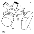
図2は、ウェルディングプレス接合法を実施するための溶接装置5を示している。この溶接装置5は、特に、ソノトローデ5.1とアンビル5.2から構成される超音波溶接装置である。
FIG. 2 shows a
極接点Pを筐体側壁3と導電性接続するため、電極スタック2は図3及び4に従ってフレーム3の中を通され、極接点Pを形成する集電タブ2.1は付属する各セル側壁3の内側に平らに互いに上下に積み重ねられる。その際必要な、電極スタック2の中央付近に対する集電タブ2.1の相対的な湾曲は、使用される電極箔の柔軟性によって達成される。
In order to conductively connect the pole contact P with the
集電タブ2.1を極接点Pへ溶接し、同時に筐体側壁3へ溶接するために、筐体側壁3の内側に当たる極接点P及び筐体側壁3がソノトローデ5.1とアンビル5.2の間に配置され、加えられたプレス力FPによってプレスされる。同時にソノトローデ5.1は超音波範囲の周波数を持つ振動Sを生成し、その結果極接点P及び筐体側壁3は大きな摩擦力の下で互いに運動する。その際に生じる大きな摩擦熱により、詳細には図示していない溶接ビード又は詳細には図示していない溶接ポイントが生じ、その結果極接点Pと筐体側壁3との間に接着結合及び導電性接続が形成される。
In order to weld the current collecting tab 2.1 to the pole contact P and simultaneously weld to the
筐体側壁3と極接点Pとの平面的な導電性接続は、特に複数の列状及び/又は平行に配置された溶接ビード及び/又は溶接ポイントによって得られる。
The planar conductive connection between the
超音波溶接プロセスのほかに別法として、詳細には図示していない、従来技術で公知のその他のウェルディングプレス接合法も生成に適している。その際、例えばコンデンサ放電溶接、抵抗プレス溶接、電気スポット溶接又は電気シーム溶接を使用してよい。 In addition to the ultrasonic welding process, other welding press joining methods known in the prior art, not shown in detail, are also suitable for production. In that case, for example, capacitor discharge welding, resistance press welding, electric spot welding or electric seam welding may be used.
詳細には図示していない本発明の一発展形態に従い、筐体側壁3と極接点Pとの導電性接続を形成する前に、集電タブ2.1は個別の方法でプレス及び/又は溶接される。
In accordance with one development of the invention not shown in detail, the current collecting tab 2.1 is pressed and / or welded in a separate manner before forming a conductive connection between the
詳細には図示していない本発明の別の一実施形態では、例えば銅で作られた極接点Pと、例えばアルミニウムで作られた筐体側壁3との間に、追加で詳細には図示していないニッケルで作られた独立した箔を挿入することにより、溶接プロセス中に極接点Pと筐体側壁3の間でより良い接続が達成される。この箔は、別法として同様に筐体側壁3の極接点Pの方を向いた側に取り付けてもよい。
In a further embodiment of the invention, not shown in detail, an additional detail is shown between a pole contact P made of, for example, copper and a
本発明の有利な一発展形態ではさらに、詳細には図示していない電気的に絶縁された箔を極接点Pと筐体側壁3の間に配置するか、又は筐体側壁3の片面を電気的に絶縁された層として形成し、その結果、極接点Pと筐体側壁3との電気的な接触は、溶接プロセス時に初めて生じる。この絶縁箔又は絶縁層は、好ましくは例えば単一セル1内の電解質に接することによって生じる腐食から筐体側壁3を保護するために、引き続き用いられる。
In a further advantageous development of the invention, an electrically insulated foil, not shown in detail, is arranged between the pole contact P and the
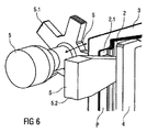
図5及び図6では、ウェルディングプレス接合法を実施するための、溶接装置5を使用して筐体側壁3と導電性接続するための溶接プロセス中の電極スタック2の斜視図を使用し、本発明の有利な実施形態を示している。
In FIGS. 5 and 6, a perspective view of the
その際、単一セル1は開いた状態で、その中で電極スタック2はまだフレーム4の中を通されておらず、又はその中に配置されておらず、集電タブ2.1によって形成された電極スタック2の極接点Pは付属するセル側壁3と導電性接続されており、その結果、電極スタック2をフレーム4に通した後で、残っている極接点Pを別のセル側壁3と導電性接続するだけでよい。特にその結果として電極スタックの取り扱いが簡単になることで、単一セル1の製造の簡素化が達成される。
In that case, the
導電性接続の形成には、示された超音波溶接プロセスの他に、従来技術で公知のウェルディングプレス接合法を使用してもよい。また、例えばレーザー溶接プロセスのような高い熱浸透を伴う溶接プロセスも使用することができる。なぜなら、示された配置は良好な熱発散を保証しており、簡単な、詳細には図示していない処置によって追加的に拡大することができるからである。 In addition to the illustrated ultrasonic welding process, a welding press joining method known in the prior art may be used to form the conductive connection. It is also possible to use welding processes with high heat penetration, such as laser welding processes. This is because the arrangement shown guarantees good heat dissipation and can be expanded further by a simple procedure not shown in detail.
1 単一セル
2 電極スタック
2.1 集電タブ
3 筐体側壁
4 フレーム
4.1 材料後退部
5 溶接装置
5.1 ソノトローデ
5.2 アンビル
FP プレス力
P 極接点
S 振動
DESCRIPTION OF
Claims (15)
After forming the conductive connection, the housing side wall (3) is fixed to the frame (4) by frictional bonding, adhesive bonding, and / or shape bonding, and the single cell (1) is filled with electrolyte. The method of claim 1.
Applications Claiming Priority (2)
| Application Number | Priority Date | Filing Date | Title |
|---|---|---|---|
| DE102008010810A DE102008010810A1 (en) | 2008-02-23 | 2008-02-23 | Method for producing a single cell for a battery |
| PCT/EP2009/001171 WO2009103519A1 (en) | 2008-02-23 | 2009-02-19 | Method for producing an individual cell for a battery |
Publications (2)
| Publication Number | Publication Date |
|---|---|
| JP2011513892A true JP2011513892A (en) | 2011-04-28 |
| JP2011513892A5 JP2011513892A5 (en) | 2012-02-16 |
Family
ID=40668162
Family Applications (1)
| Application Number | Title | Priority Date | Filing Date |
|---|---|---|---|
| JP2010547104A Pending JP2011513892A (en) | 2008-02-23 | 2009-02-19 | Method for producing single cell for battery |
Country Status (7)
| Country | Link |
|---|---|
| US (1) | US20110035934A1 (en) |
| EP (1) | EP2243179B1 (en) |
| JP (1) | JP2011513892A (en) |
| CN (1) | CN101946345A (en) |
| AT (1) | ATE540441T1 (en) |
| DE (1) | DE102008010810A1 (en) |
| WO (1) | WO2009103519A1 (en) |
Families Citing this family (2)
| Publication number | Priority date | Publication date | Assignee | Title |
|---|---|---|---|---|
| DE102010005083A1 (en) | 2010-01-20 | 2010-08-12 | Daimler Ag | Device for the production of an electrochemical single cell surrounded by a single cell housing in motor vehicles comprises a fixing aid formed by holding elements which slide against each other |
| DE102010023092A1 (en) * | 2010-05-31 | 2011-12-01 | Varta Microbattery Gmbh | Battery, method of making a battery and circuit with a battery |
Family Cites Families (7)
| Publication number | Priority date | Publication date | Assignee | Title |
|---|---|---|---|---|
| US5567544A (en) * | 1995-05-26 | 1996-10-22 | Boundless Corp. | Battery |
| DE19936063B4 (en) * | 1999-07-30 | 2004-03-04 | Cochlear Ltd., Lane Cove | Electrochemical secondary cell |
| US6405815B1 (en) * | 2000-01-06 | 2002-06-18 | Case Corp. | Nestable fluid coupler |
| US6406815B1 (en) * | 2000-02-11 | 2002-06-18 | Delphi Technologies, Inc. | Compact lithium ion battery and method of manufacturing |
| JP2004134210A (en) * | 2002-10-10 | 2004-04-30 | Nissan Motor Co Ltd | Lamination type battery, battery pack, and vehicle |
| US7476463B2 (en) * | 2003-08-15 | 2009-01-13 | Pacific Lithium New Zealand Limited | Rechargeable bipolar high power electrochemical device with reduced monitoring requirement |
| DE102007063181B4 (en) | 2007-08-06 | 2010-12-30 | Daimler Ag | Single cell for a battery and method for its production |
-
2008
- 2008-02-23 DE DE102008010810A patent/DE102008010810A1/en not_active Withdrawn
-
2009
- 2009-02-19 WO PCT/EP2009/001171 patent/WO2009103519A1/en active Application Filing
- 2009-02-19 EP EP09712006A patent/EP2243179B1/en not_active Not-in-force
- 2009-02-19 US US12/918,598 patent/US20110035934A1/en not_active Abandoned
- 2009-02-19 AT AT09712006T patent/ATE540441T1/en active
- 2009-02-19 CN CN2009801047765A patent/CN101946345A/en active Pending
- 2009-02-19 JP JP2010547104A patent/JP2011513892A/en active Pending
Also Published As
| Publication number | Publication date |
|---|---|
| CN101946345A (en) | 2011-01-12 |
| EP2243179A1 (en) | 2010-10-27 |
| WO2009103519A1 (en) | 2009-08-27 |
| EP2243179B1 (en) | 2012-01-04 |
| ATE540441T1 (en) | 2012-01-15 |
| DE102008010810A1 (en) | 2009-08-27 |
| US20110035934A1 (en) | 2011-02-17 |
Similar Documents
| Publication | Publication Date | Title |
|---|---|---|
| JP5476302B2 (en) | Individual cell for battery and manufacturing method thereof | |
| KR100599732B1 (en) | Secondary battery | |
| KR100590006B1 (en) | Secondary battery and electrodes assembly | |
| US8986874B2 (en) | Prismatic cell and production method for the same | |
| KR101715954B1 (en) | Secondary battery | |
| US11923558B2 (en) | Rectangular secondary battery | |
| US10411227B2 (en) | Energy storage device, energy storage apparatus and method of manufacturing energy storage device | |
| CN112534637B (en) | secondary battery | |
| JP2006040902A (en) | Secondary battery and manufacturing method of secondary battery | |
| US20200251711A1 (en) | Rectangular secondary battery and method of manufacturing the same | |
| JP6117927B2 (en) | Secondary battery | |
| CN101772852A (en) | Single cell for a battery for making electrical contact | |
| JP2020513148A (en) | Electrode having improved electrode tab welding characteristics and secondary battery including the same | |
| KR100627360B1 (en) | Plate used to collect current, secondary battery and module thereof | |
| US20200274132A1 (en) | Electrical cell connection arrangements and method thereof | |
| JP2023537846A (en) | Cylindrical battery cells, battery packs and automobiles containing same | |
| US11404754B2 (en) | Secondary battery | |
| CN110165099A (en) | The manufacturing method of battery pack and battery pack | |
| KR101753938B1 (en) | Secondary battery with improved electric insulation and manufacture method thereof | |
| CN217361685U (en) | Battery, and battery pack and vehicle including the same | |
| JP2022049725A (en) | Secondary battery terminal and method of manufacturing the same | |
| US10263291B2 (en) | Method of producing a prismatic battery cell | |
| KR100612236B1 (en) | Secondary battery and electrodes assembly | |
| KR101712449B1 (en) | A hollow-shaped jelly roll tap plate assembly | |
| JP2011513892A (en) | Method for producing single cell for battery |
Legal Events
| Date | Code | Title | Description |
|---|---|---|---|
| A521 | Request for written amendment filed |
Free format text: JAPANESE INTERMEDIATE CODE: A523 Effective date: 20111221 |
|
| A621 | Written request for application examination |
Free format text: JAPANESE INTERMEDIATE CODE: A621 Effective date: 20111221 |
|
| A131 | Notification of reasons for refusal |
Free format text: JAPANESE INTERMEDIATE CODE: A131 Effective date: 20130702 |
|
| A02 | Decision of refusal |
Free format text: JAPANESE INTERMEDIATE CODE: A02 Effective date: 20131203 |