JP2011106958A - Current detector - Google Patents
Current detector Download PDFInfo
- Publication number
- JP2011106958A JP2011106958A JP2009262171A JP2009262171A JP2011106958A JP 2011106958 A JP2011106958 A JP 2011106958A JP 2009262171 A JP2009262171 A JP 2009262171A JP 2009262171 A JP2009262171 A JP 2009262171A JP 2011106958 A JP2011106958 A JP 2011106958A
- Authority
- JP
- Japan
- Prior art keywords
- magnetic core
- core
- conversion element
- unit
- current detection
- Prior art date
- Legal status (The legal status is an assumption and is not a legal conclusion. Google has not performed a legal analysis and makes no representation as to the accuracy of the status listed.)
- Pending
Links
- 239000000463 material Substances 0.000 claims abstract description 39
- 238000006243 chemical reaction Methods 0.000 claims abstract description 36
- 230000004907 flux Effects 0.000 claims abstract description 6
- 238000001514 detection method Methods 0.000 claims description 32
- 238000003780 insertion Methods 0.000 claims description 18
- 230000037431 insertion Effects 0.000 claims description 18
- 239000004020 conductor Substances 0.000 claims description 15
- 238000000465 moulding Methods 0.000 claims description 8
- 239000011347 resin Substances 0.000 description 8
- 229920005989 resin Polymers 0.000 description 8
- 238000000034 method Methods 0.000 description 5
- 239000004698 Polyethylene Substances 0.000 description 4
- 239000004743 Polypropylene Substances 0.000 description 4
- 230000000694 effects Effects 0.000 description 4
- 229920001707 polybutylene terephthalate Polymers 0.000 description 4
- 229920000573 polyethylene Polymers 0.000 description 4
- 229920001155 polypropylene Polymers 0.000 description 4
- 239000004677 Nylon Substances 0.000 description 3
- 238000005452 bending Methods 0.000 description 3
- 229920001778 nylon Polymers 0.000 description 3
- -1 polybutylene terephthalate Polymers 0.000 description 3
- 239000000470 constituent Substances 0.000 description 2
- 238000010586 diagram Methods 0.000 description 2
- 239000000945 filler Substances 0.000 description 2
- 239000003365 glass fiber Substances 0.000 description 2
- RYGMFSIKBFXOCR-UHFFFAOYSA-N Copper Chemical compound [Cu] RYGMFSIKBFXOCR-UHFFFAOYSA-N 0.000 description 1
- 239000003990 capacitor Substances 0.000 description 1
- 229910052802 copper Inorganic materials 0.000 description 1
- 239000010949 copper Substances 0.000 description 1
- 238000003754 machining Methods 0.000 description 1
- 239000002184 metal Substances 0.000 description 1
- 229910052751 metal Inorganic materials 0.000 description 1
Images


Landscapes
- Measuring Instrument Details And Bridges, And Automatic Balancing Devices (AREA)
Abstract
Description
本発明は、電流検出装置に関する。 The present invention relates to a current detection device.
車両等に搭載される電気接続箱には、電流検出装置が取り付けられる場合がある。このような電流検出装置としてはたとえば特許文献1に記載のものなどが知られている。 A current detection device may be attached to an electrical junction box mounted on a vehicle or the like. As such a current detection device, for example, the one described in Patent Document 1 is known.
特許文献1には、1つの樹脂ケースに、磁性体コアと、磁性体コアの挿通部に挿通されて電流検出対象となる導体と、磁性体コアのギャップ部に配されて導体を流れる電流により発生した磁束を検出する磁電変換素子と、が収容された電流検出装置が記載されている(特許文献1の図1および図6などを参照)。 In Patent Document 1, a single resin case is provided with a magnetic core, a conductor that is inserted into the insertion portion of the magnetic core, and a current detection target, and a current that is disposed in the gap portion of the magnetic core and flows through the conductor. A current detection device in which a magnetoelectric conversion element for detecting generated magnetic flux is housed is described (see FIGS. 1 and 6 of Patent Document 1).
ところで、電流検出装置を構成する部材を収容するケースの材料としては、ケースに求められる性能を満たすものが用いられる。たとえば特許文献1に記載の電流検出装置では、磁性体コアを保持するコア保持部が設けられているが、当該コア保持部では高い保持力が求められるため、剛性の高い材料を用いることが必要となる。また磁電変換素子とコアのギャップ部との位置合わせを正確に行うため、加工精度がよく、熱変形が少ない材料を用いることが必要である。 By the way, as a material of the case that accommodates the members constituting the current detection device, a material that satisfies the performance required for the case is used. For example, in the current detection device described in Patent Document 1, a core holding portion that holds a magnetic core is provided. However, since the core holding portion requires a high holding force, it is necessary to use a material having high rigidity. It becomes. In addition, in order to accurately align the magnetoelectric conversion element and the gap portion of the core, it is necessary to use a material with high processing accuracy and less thermal deformation.
しかし、上記特許文献1に記載の電流検出装置のように、磁電変換素子と磁性体コアなどの構成部材を1つのケースに収容する場合には、ケース全体を同じ材料で作製するのが一般的であるので、このような場合には、一部において求められる特性を満たすために、ケース全体を高価な材料を用いて作製する必要が生じ得る。
本発明は上記のような事情に基づいて完成されたものであって、コストを低減した電流検出装置を提供することを目的とする。
However, when the structural members such as the magnetoelectric conversion element and the magnetic core are accommodated in one case as in the current detection device described in Patent Document 1, the entire case is generally made of the same material. Therefore, in such a case, it may be necessary to fabricate the entire case using an expensive material in order to satisfy some required characteristics.
The present invention has been completed based on the above-described circumstances, and an object thereof is to provide a current detection device with reduced cost.
上記課題を解決するものとして、本発明は、ギャップ部が設けられた磁性体コア、および前記磁性体コアを収容するハウジングを有するコアユニットと、前記ギャップ部に配置されて前記磁性体コアで生じる磁束を検出する磁電変換素子、前記磁電変換素子に接続される配索材、および前記配索材を収容するとともに前記磁電変換素子を外側に配置した本体部を有し、かつ前記コアユニットとは別体の電子ユニットと、を備えることを特徴とする電流検出装置である。 In order to solve the above-mentioned problems, the present invention arises in the magnetic core that is disposed in the gap portion and a core unit that has a magnetic core provided with a gap portion, and a housing that houses the magnetic core. A magnetoelectric conversion element that detects magnetic flux, a wiring material connected to the magnetoelectric conversion element, a main body that houses the wiring material and has the magnetoelectric conversion element disposed outside, and the core unit And a separate electronic unit.
上述したように、磁電変換素子と磁性体コアなどの構成部材を1つの樹脂ケースに収容する場合には、樹脂ケースの材料としては一種類の樹脂が用いられるのが一般的である。これに対して、本発明では、コアユニットと電子ユニットとが別体であるので、各ユニットあるいはユニットを構成する部品の一部を異なる材料を用いて作製することができる。本発明の構造では、磁電変換素子と磁性体コアとの位置合わせを精度よく行うことが出来る構造とするのが好ましいのであるが、本発明においては、例えば位置合わせに介在する部分のみ加工精度が良い材料を用いて、それ以外は安価な材料を用いることが可能である。その結果、本発明によれば、装置全体としてのコストを低減するという効果が得られるのである。 As described above, when the structural members such as the magnetoelectric conversion element and the magnetic core are accommodated in one resin case, one type of resin is generally used as the material of the resin case. On the other hand, in the present invention, since the core unit and the electronic unit are separate, each unit or part of the components constituting the unit can be manufactured using different materials. In the structure of the present invention, it is preferable that the magnetoelectric conversion element and the magnetic core can be aligned with high accuracy. However, in the present invention, for example, only the portion interposed in the alignment has processing accuracy. It is possible to use a good material and an otherwise inexpensive material. As a result, according to the present invention, an effect of reducing the cost of the entire apparatus can be obtained.
本発明は以下の構成であってもよい。
前記電子ユニットの本体部および前記コアユニットのハウジングのうち、いずれか一方には係合部が形成され、他方には前記係合部が係合可能な被係合部が形成されている構成であってもよい。この構成によれば、係合部と被係合部とを係合させることにより、電子ユニットとコアユニットの位置合わせを容易かつ確実に行うことができる。
The present invention may have the following configuration.
An engagement portion is formed on one of the main body portion of the electronic unit and the housing of the core unit, and an engaged portion on which the engagement portion can be engaged is formed on the other. There may be. According to this configuration, the electronic unit and the core unit can be easily and reliably aligned by engaging the engaging portion and the engaged portion.
前記磁電変換素子は、前記磁性体コアの厚み方向に対して略平行な方向に差し込むことにより前記ギャップ部に配置されていてもよい。このような構成とすると、磁電変換素子を有する電子ユニットと磁性体コアを有するコアユニットとが一部または全域にわたって重なり合うので電流検出装置の投影面積を小さくすることができる。その結果、電流検出装置を小型化することができる。 The magnetoelectric conversion element may be disposed in the gap portion by being inserted in a direction substantially parallel to the thickness direction of the magnetic core. With such a configuration, since the electronic unit having the magnetoelectric conversion element and the core unit having the magnetic core overlap partly or entirely, the projected area of the current detection device can be reduced. As a result, the current detection device can be reduced in size.
前記電子ユニットは、前記本体部と着脱自在に結合して外部機器と前記磁電変換素子とを電気的に接続するコネクタ部を備えていてもよい。このような構成とすると、外部機器と磁電変換素子との電気的な接続を容易に行うことができる。 The electronic unit may include a connector portion that is detachably coupled to the main body portion and electrically connects an external device and the magnetoelectric conversion element. With such a configuration, electrical connection between the external device and the magnetoelectric conversion element can be easily performed.
前記磁性体コアは電流検出対象である導体を挿通可能な挿通部を有し、前記コアユニットにおいて、前記導体が前記磁性体コアの挿通部に挿通された状態で、前記ハウジングとがモールド成形により一体化されていてもよい。 The magnetic core has an insertion portion through which a conductor that is a current detection target can be inserted, and in the core unit, the conductor is inserted into the insertion portion of the magnetic core, and the housing is molded by molding. It may be integrated.
前記導体に、前記磁性体コアのギャップ部の幅寸法以下に形成され前記ギャップ部を挿通可能な挿通可能部を設けてもよい。このような構成とすると、磁性体コアをより小型化することができる。 The conductor may be provided with an insertable part that is formed to be equal to or smaller than the width of the gap part of the magnetic core and that can be inserted through the gap part. With such a configuration, the magnetic core can be further downsized.
本発明によれば、コストを低減した電流検出装置を提供することができる。 According to the present invention, it is possible to provide a current detection device with reduced cost.
<実施形態1>
本発明の実施形態1を図1ないし図4によって説明する。
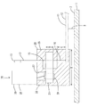
本実施形態の電流検出装置10は、図1に示すように、磁性体コア21と磁性体コア21を収容するハウジング25を有するコアユニット20と、このコアユニット20に重ねられた略直方体状の電子ユニット30と、を備える。
まず、コアユニット20について説明する。コアユニット20のハウジング25の上面と図1に示す右側側面からは、銅などの導電性材料からなるバスバー11(導体)が突出している。バスバー11はハウジング25の側面から突出し電気接続箱1の底面2に対して略平行に配されたバスバー本体部12と、バスバー本体部12から略垂直に立ち上げられた起立部17とを有し、略L字状をなしている。バスバー本体部12は電気接続箱1の底面2に設けた台3に載置されている。
<Embodiment 1>
A first embodiment of the present invention will be described with reference to FIGS.
As shown in FIG. 1, the
First, the
バスバー11の起立部17の上端には、バッテリやインバータなどの他の部材(図示せず)と接続される端子部13が設けられている。この端子部13の大きさはバスバー11を流れる電流の量によって決定される。バスバー11の端子部13の下側には、図2に示すように、端子部13よりも幅寸法を小さくした首部14と、U字状をなすU字部15と、U字部15よりもさらに幅寸法の小さいくびれ部16(挿通可能部16)が連なっている。バスバー11のU字部15は、展開形状がくびれ部16よりも幅広な部分を、磁性体コア21のバスバー挿通部23を挿通可能なサイズに折り曲げ加工を施すことにより形成されている。
バスバー11の起立部17の下端は略垂直に折り曲げられてバスバー本体部12に連なっている。バスバー11のU字部15とバスバー本体部12の断面積は、バスバー11の成形歩留まりを向上させるため同程度であるのが好ましい。
A
The lower end of the standing
くびれ部16は、幅寸法が磁性体コア21のギャップ部22の幅寸法A以下であるとともに、その長さCが磁性体コア21の厚み寸法B以上となるように形成されており、磁性体コア21のギャップ部22を円滑に差し込むことができるようになっている。本実施形態では、くびれ部16の長さCは、磁性体コア21の厚み寸法Bより少し大きくなるように、すなわち、磁性体コア21を取り付けるのに必要な最小限の長さとなるように設定されている。
The
磁性体コア21は図2および図3に示すように、略C字状をなしており、磁束を検出する磁電変換素子31が配置されるギャップ部22と、バスバー11が挿通されるバスバー挿通部23(導体挿通部23)とが設けられている。
2 and 3, the
磁性体コア21を収容するハウジング25と、バスバー11が挿通された状態の磁性体コア21とは、モールド成形により一体化されている。
ハウジング25を構成する材料としては、ポリブチレンテレフタレート(PBT)、ナイロン、ポリプロピレン(PP)、ポリエチレン(PE)などの各種樹脂材料が挙げられる。これらの材料にはガラス繊維などのフィラーが入っていてもよい。これらのうち、位置合わせに介在しない部分をの材料としてPP、PEなどの安価な樹脂を用いるのが好ましい。
The
Examples of the material constituting the
ハウジング25の上面には、磁性体コア21のギャップ部22の直上に相当する位置に、後述する磁電変換素子31が挿通可能な素子挿通孔27が形成されている。また、ハウジング25の上面には、電子ユニット30の本体部32に形成されている2つの係合凸部33,33(係合部)と係合可能な2つの係合孔26,26(被係合部)が形成されている(図2および図3を参照)。
On the upper surface of the
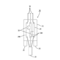
次に電子ユニット30について説明する。電子ユニット30は、磁性体コア21のギャップ部22に配置されて磁性体コア21で生じる磁束を検出する磁電変換素子31と、磁電変換素子31に接続される配索材34と、配索材34を収容する本体部32とを有する。
Next, the
電子ユニット30の本体部32は、図2に示すように、略直方体状をなしており、本体部32の上面からは外部機器(図示せず)と接続される電線36が導出されており、本体部32の下端には2つの係合凸部33,33が形成されている。
本体部32の内部は、図4および図5に示すように、静電気防止コンデンサなどの電子部品35と、磁電変換素子31と外部機器とを電気的に接続する配索材34とが収容されている。
As shown in FIG. 2, the
As shown in FIGS. 4 and 5, an
配索材34としては、例えば、図4に示すようなプリント基板34Aや図5に示すようなバスバー34B(以下、「内部バスバー34B」という)などを用いることができる。
図4では配索材34としてプリント基板34Aを用いた本体部32の内部を模式的に示している。図4に示すように、プリント基板34Aには電子部品35が実装されており、その上端側には外部機器に接続された電線36の端末が接続され、下端側には磁電変換素子31が接続される。
As the
FIG. 4 schematically shows the inside of the
図5では配索材34として内部バスバー34Bを用いた本体部32の内部を模式的に示している。図5に示すように、電子部品35は隣接する内部バスバー34Bを繋げるように配置され、内部バスバー34Bの上端部側に外部機器に接続された電線36の端末が接続され、内部バスバー34Bの下端部側に磁電変換素子31が接続される。
FIG. 5 schematically shows the inside of the
配索材34に接続された磁電変換素子31は、図1および図2に示すように係合凸部33よりも下側、つまり本体部32の下端部よりも下側(本体部32の外側)に配されている。
As shown in FIGS. 1 and 2, the
電子ユニット30の本体部32は樹脂材料をモールド成形するなどの方法により作製される。本体部32を構成する材料としては、PBT、ナイロン、PP、PEなどの各種樹脂材料が挙げられる。これらの材料にはガラス繊維などのフィラーが入っていてもよい。電子ユニット30の本体部32の材料としては、コアユニット20に取り付けられた際のがたつきを防止するという観点からPBTやナイロンなどの剛性の高い材料を用いるのが好ましい。
The
次に、電子ユニット30をコアユニット20に組み付ける方法について説明する。
まずコアユニット20を作製する。導電性の金属板から、所定形状のバスバー11を切り出し、図1および図2に示すような形状となるように曲げ加工などを施す。このようにして作製したバスバー11に、以下の手順により磁性体コア21を取り付ける。まず、磁性体コア21のギャップ部22をバスバー11のくびれ部16に差し込む。本実施形態において、バスバー11のくびれ部16は、幅寸法が磁性体コア21のギャップ部22の幅寸法A以下であるとともに、その長さCが磁性体コア21の厚み寸法B以上に形成されているので、磁性体コア21のギャップ部22を円滑に差し込むことができる。
Next, a method for assembling the
First, the
次に、バスバー11のU字部15に磁性体コア21のバスバー挿通部23が配されるように、バスバー11または磁性体コア21を移動させる。ここで、U字部15は予めバスバー挿通部23を挿通可能に加工されているので、磁性体コア21のバスバー挿通部23に挿通させることができる。
Next, the
次に、バスバー11を挿通させた状態の磁性体コア21とハウジング25とを、モールド成形により一体化することでコアユニット20が得られる。このようにして作製したコアユニット20を電気接続箱1の底面2の所定位置に取り付ける。
次に、電子ユニット30の本体部32に配索材34を収容し、この配索材34に外部機器に接続された電線36の端末と磁電変換素子31とを接続することにより電子ユニット30を作製する。
Next, the
Next, the
このようにして作製した電子ユニット30の磁電変換素子31を、図1および図2における上側からコアユニット20の素子挿通孔27(磁性体コア21の厚み方向に対して略平行な方向)に差し込んで磁性体コア21のギャップ部22に配置し、電子ユニット30の係合凸部33をコアユニット20の係合孔26に係合させることにより、電子ユニット30がコアユニット20の所定位置に組みつけられる。電子ユニット30がコアユニット20に組みつけられた状態において、電子ユニット30は、図3に示すように、コアユニット20の投影面積の範囲内にある。
The
次に、本実施形態の効果について説明する。
本実施形態では、コアユニット20と電子ユニット30とが別体であるので、各ユニットを別々の材料を用いて作製することができる。例えば電子ユニット30とコアユニット20の材料として位置合わせに介在する部分のみ加工精度が良い材料を用い、それ以外は安価な材料を用いて二色成形により各ユニットを作製することが可能である。その結果、本実施形態によれば、電流検出装置10全体としてのコストを低減することができる。
Next, the effect of this embodiment will be described.
In this embodiment, since the
また、本実施形態では、磁電変換素子31は、図2における上側から下側方向(磁性体コア21の厚み方向に対して略平行な方向)に差し込むことによりギャップ部22に配置されているから、電子ユニット30とコアユニット20とが全域にわたって重なり合うので電流検出装置10の投影面積を小さくすることができる。その結果、本実施形態によれば、電流検出装置10を小型化することができる。
Further, in the present embodiment, the
特に、本実施形態では、バスバー11に、磁性体コア21のギャップ部22の幅寸法以下に形成されギャップ部22を挿通可能なくびれ部16(挿通可能部16)を設けたから、磁性体コア21をより小型化することができる。なお、バスバー11に幅寸法の小さい部分を設けると、バスバー11の抵抗値の増大が懸念されるが、本実施形態によれば、くびれ部16の長さが、磁性体コア21を取り付けるのに必要な最小限の長さに設定されており、くびれ部16に隣接して展開形状が幅広なU字部15を設けているから、バスバー11の抵抗値の増大を確実に防止することができる。
In particular, in the present embodiment, the
また、本実施形態によれば、電子ユニット30の本体部32に2つの係合凸部33,33が形成され、コアユニット20のハウジング25には係合凸部33,33が係合可能な2つの係合孔26,26が形成されているから、電子ユニット30とコアユニット20の位置合わせを容易かつ確実に行うことができる。
Further, according to the present embodiment, the two engaging
<実施形態2>
次に、本発明の実施形態2を図6によって説明する。本実施形態は、電子ユニット30が、本体部32と着脱自在に結合して外部機器と磁電変換素子31とを電気的に接続するコネクタ部40を備える点で実施形態1と相違する。上記実施形態1と同様の構成部位については同一符号を付して重複する記載は省略する。
<
Next,
電子ユニット30の本体部32には、図6に示すように、複数の端子37が端子37の先端部を上方に向けた状態で設けられている。本体部32と電線36の端末が接続されたコネクタ部40とは互いに嵌合可能となっている。本体部32とコネクタ部40とは嵌合が終了すると、公知の構成のロック機構により係止される。その他の構成や作用効果は実施形態1と概ね同様である。
本実施形態によれば、本体部32と着脱自在に結合するコネクタ部40を備えるので、外部機器と磁電変換素子31との電気的な接続を容易に行うことができる。
As shown in FIG. 6, a plurality of
According to this embodiment, since the
<実施形態3>
次に、本発明の実施形態3を図7によって説明する。本実施形態は、磁電変換素子31を差し込む方向が磁性体コア21の厚み方向に対して略垂直な方向であるという点で、実施形態1と相違する。上記実施形態1と同様の構成部位については同一符号を付して重複する記載は省略する。
本実施形態では、図7に示すように、ハウジング25の側面(図7における左側の側面)に、磁電変換素子31が挿通可能な素子挿通孔27と、2つの係合孔26とが形成されている。
<
Next,
In the present embodiment, as shown in FIG. 7, an
本実施形態では、磁電変換素子31を、図7における左側からコアユニット20の素子挿通孔27(磁性体コア21の厚み方向に対して略垂直な方向)に差し込んで磁性体コア21のギャップ部22に配置し、電子ユニット30の係合凸部33をコアユニット20の係合孔26に係合させることにより、電子ユニット30がコアユニット20の所定位置に組みつけられる。
In the present embodiment, the
電子ユニット30がコアユニット20に組みつけられた状態において、電子ユニット30は、図7に示すように、コアユニット20と並列した位置に配される。その他の構成や作用効果はは実施形態1と概ね同様である。
本実施形態によれば、磁電変換素子31を差し込む方向が磁性体コア21の厚み方向に対して略垂直な方向であるので、電流検出装置10を高さ方向において省スペースなものとすることができる。
In a state where the
According to the present embodiment, since the direction in which the
<他の実施形態>
本発明は上記記述及び図面によって説明した実施形態に限定されるものではなく、例えば次のような実施形態も本発明の技術的範囲に含まれる。
(1)上記実施形態では、係合部と被係合部として、電子ユニット30の本体部32に2つの係合凸部33,33を設け、コアユニット20のハウジング25に2つの係合孔26,26を設けたものを示したが、係合凸部33や係合孔26の数は1つであっても3以上であってもよいし、これらを設けなくてもよい。また、電子ユニット30の本体部32に係合孔26を設けハウジング25に係合凸部33を設けたものであってもよいし別の形態の係合部や被係合部を設けてもよい。
<Other embodiments>
The present invention is not limited to the embodiments described with reference to the above description and drawings. For example, the following embodiments are also included in the technical scope of the present invention.
(1) In the above embodiment, as the engaging portion and the engaged portion, the two engaging
(2)上記実施形態では、磁性体コア21のバスバー挿通部23に挿通された状態のバスバー11とハウジング25とがモールド成形により一体化されているものを示したが、ハウジング25にバスバー11の係止部を設けてバスバー11を固定してもよい。
(2) In the above embodiment, the
(3)上記実施形態では、磁性体コア21のギャップ部22の幅寸法A以下の幅寸法の部分(くびれ部16)を設けたバスバー11を示したが、ギャップ部22の幅寸法A以下となるようにバスバー11に曲げ加工を施すことにより図8に示すように略C字状をなすC字部15aを設けてもよい。このようにすることにより、図9に示すように、くびれ部16の長さC1を短くでき、電流検出装置10を高さ方向において省スペースなものとすることが出来る。またU字部15を設けた実施形態1の電流検出装置10(幅寸法は図1中のD)よりも、C字部15aを設けた電流検出装置10において幅寸法D1を小さくすることができ、これにより省スペースとすることができる。なお、この形態のバスバー11に磁性体コア21を取り付ける際には、バスバー11のC字部15aのうちギャップ部22の幅寸法A以下の部分を磁性体コア21のギャップ部22に挿通させてからバスバー11を所定位置に配する。
(3) In the above-described embodiment, the
10…電流検出装置9
11…バスバー
12…バスバー本体部
16…くびれ部(挿通可能部)
20…コアユニット
21…磁性体コア
22…ギャップ部
23…バスバー挿通部(導体挿通部)
25…ハウジング
26…係合孔(被係合部)
30…電子ユニット
31…磁電変換素子
32…(電子ユニットの)本体部
33…係合凸部(係合部)
34…配索材
35…電子部品
36…電線(外部機器に接続された電線)
40…コネクタ部
10: Current detection device 9
11 ...
DESCRIPTION OF
25 ...
DESCRIPTION OF
34 ...
40 ... Connector
Claims (6)
前記ギャップ部に配置されて前記磁性体コアで生じる磁束を検出する磁電変換素子、前記磁電変換素子に接続される配索材、および前記配索材を収容するとともに前記磁電変換素子を外側に配置した本体部を有し、かつ前記コアユニットとは別体の電子ユニットと、を備えることを特徴とする電流検出装置。 A magnetic core provided with a gap portion, and a core unit having a housing for accommodating the magnetic core;
A magnetoelectric conversion element that detects magnetic flux generated in the magnetic core disposed in the gap portion, a wiring material connected to the magnetoelectric conversion element, and the wiring material are accommodated and the magnetoelectric conversion element is disposed outside. A current detecting device comprising: an electronic unit that is separate from the core unit.
前記コアユニットにおいて、前記導体が前記磁性体コアの導体挿通部に挿通された状態で、前記ハウジングとモールド成形により一体化されていることを特徴とする請求項1ないし請求項4のいずれか一項に記載の電流検出装置。 The magnetic core has a conductor insertion portion through which a conductor that is a current detection target can be inserted,
5. The core unit according to claim 1, wherein the conductor is integrated with the housing by molding in a state where the conductor is inserted through a conductor insertion portion of the magnetic core. The current detection device according to item.
Priority Applications (1)
| Application Number | Priority Date | Filing Date | Title |
|---|---|---|---|
| JP2009262171A JP2011106958A (en) | 2009-11-17 | 2009-11-17 | Current detector |
Applications Claiming Priority (1)
| Application Number | Priority Date | Filing Date | Title |
|---|---|---|---|
| JP2009262171A JP2011106958A (en) | 2009-11-17 | 2009-11-17 | Current detector |
Publications (1)
| Publication Number | Publication Date |
|---|---|
| JP2011106958A true JP2011106958A (en) | 2011-06-02 |
Family
ID=44230604
Family Applications (1)
| Application Number | Title | Priority Date | Filing Date |
|---|---|---|---|
| JP2009262171A Pending JP2011106958A (en) | 2009-11-17 | 2009-11-17 | Current detector |
Country Status (1)
| Country | Link |
|---|---|
| JP (1) | JP2011106958A (en) |
Citations (3)
| Publication number | Priority date | Publication date | Assignee | Title |
|---|---|---|---|---|
| JPH09189722A (en) * | 1996-01-10 | 1997-07-22 | Tokin Corp | Current detector |
| JP2007171156A (en) * | 2005-11-22 | 2007-07-05 | Asahi Kasei Corp | Current detection element and manufacturing method thereof |
| JP2009042003A (en) * | 2007-08-07 | 2009-02-26 | Denso Corp | Current sensor |
-
2009
- 2009-11-17 JP JP2009262171A patent/JP2011106958A/en active Pending
Patent Citations (3)
| Publication number | Priority date | Publication date | Assignee | Title |
|---|---|---|---|---|
| JPH09189722A (en) * | 1996-01-10 | 1997-07-22 | Tokin Corp | Current detector |
| JP2007171156A (en) * | 2005-11-22 | 2007-07-05 | Asahi Kasei Corp | Current detection element and manufacturing method thereof |
| JP2009042003A (en) * | 2007-08-07 | 2009-02-26 | Denso Corp | Current sensor |
Similar Documents
| Publication | Publication Date | Title |
|---|---|---|
| US10971914B2 (en) | Circuit assembly | |
| JP5794938B2 (en) | High voltage electrical junction box | |
| US9086440B2 (en) | Current sensor | |
| JP5724660B2 (en) | Current detector | |
| JP5817508B2 (en) | Current detector | |
| JP5714716B2 (en) | Power control device | |
| JP2011064648A (en) | Current sensor | |
| JP2013120177A (en) | Current detector | |
| WO2014064950A1 (en) | Current sensor | |
| CN109564812B (en) | Coil assembly, circuit structure, and electrical junction box | |
| JP6709958B2 (en) | Wiring equipment | |
| JP5532843B2 (en) | Current detector | |
| JP2009268291A (en) | Circuit case with terminal | |
| JP5459195B2 (en) | Circuit assembly and electrical junction box | |
| JP2011106958A (en) | Current detector | |
| JP2012058199A (en) | Current detection apparatus | |
| JP7234847B2 (en) | electronic module | |
| JP2023161360A (en) | electrical junction box | |
| JP2015108553A (en) | Current detector | |
| JP2013044671A (en) | Current detector | |
| CN103812064B (en) | Electrical junction box | |
| JP5854282B2 (en) | Current sensor and battery module | |
| JP2011174756A (en) | Current detection device | |
| JP2013099158A (en) | Connector for inverter device | |
| JP2011185769A (en) | Current detection device and electrical junction box |
Legal Events
| Date | Code | Title | Description |
|---|---|---|---|
| A621 | Written request for application examination |
Free format text: JAPANESE INTERMEDIATE CODE: A621 Effective date: 20120907 |
|
| A977 | Report on retrieval |
Free format text: JAPANESE INTERMEDIATE CODE: A971007 Effective date: 20131023 |
|
| A131 | Notification of reasons for refusal |
Free format text: JAPANESE INTERMEDIATE CODE: A131 Effective date: 20131024 |
|
| A02 | Decision of refusal |
Free format text: JAPANESE INTERMEDIATE CODE: A02 Effective date: 20140403 |